CN115509091A - Exposure apparatus, exposure method, and method for manufacturing product - Google Patents
Exposure apparatus, exposure method, and method for manufacturing product Download PDFInfo
- Publication number
- CN115509091A CN115509091A CN202210717284.0A CN202210717284A CN115509091A CN 115509091 A CN115509091 A CN 115509091A CN 202210717284 A CN202210717284 A CN 202210717284A CN 115509091 A CN115509091 A CN 115509091A
- Authority
- CN
- China
- Prior art keywords
- illumination light
- wavelength
- optical system
- original
- exposure apparatus
- Prior art date
- Legal status (The legal status is an assumption and is not a legal conclusion. Google has not performed a legal analysis and makes no representation as to the accuracy of the status listed.)
- Pending
Links
- 238000000034 method Methods 0.000 title claims abstract description 42
- 238000004519 manufacturing process Methods 0.000 title claims abstract description 15
- 230000003287 optical effect Effects 0.000 claims abstract description 197
- 238000005286 illumination Methods 0.000 claims abstract description 110
- 239000000758 substrate Substances 0.000 claims abstract description 74
- 239000004065 semiconductor Substances 0.000 claims description 33
- 230000004075 alteration Effects 0.000 claims description 32
- 206010010071 Coma Diseases 0.000 claims description 4
- 230000001678 irradiating effect Effects 0.000 claims description 3
- 238000004590 computer program Methods 0.000 claims 1
- 238000009826 distribution Methods 0.000 description 30
- 210000001747 pupil Anatomy 0.000 description 24
- 238000010586 diagram Methods 0.000 description 20
- 150000002500 ions Chemical class 0.000 description 12
- 230000008569 process Effects 0.000 description 11
- XUIMIQQOPSSXEZ-UHFFFAOYSA-N Silicon Chemical compound [Si] XUIMIQQOPSSXEZ-UHFFFAOYSA-N 0.000 description 9
- 238000003384 imaging method Methods 0.000 description 9
- 229910052710 silicon Inorganic materials 0.000 description 9
- 239000010703 silicon Substances 0.000 description 9
- 230000007423 decrease Effects 0.000 description 8
- 239000012212 insulator Substances 0.000 description 7
- 230000010355 oscillation Effects 0.000 description 7
- 239000000463 material Substances 0.000 description 6
- 238000004088 simulation Methods 0.000 description 6
- 238000001228 spectrum Methods 0.000 description 6
- 238000005530 etching Methods 0.000 description 5
- 230000015654 memory Effects 0.000 description 5
- 230000000694 effects Effects 0.000 description 4
- 238000005247 gettering Methods 0.000 description 4
- 230000002093 peripheral effect Effects 0.000 description 4
- OKTJSMMVPCPJKN-UHFFFAOYSA-N Carbon Chemical compound [C] OKTJSMMVPCPJKN-UHFFFAOYSA-N 0.000 description 3
- 230000001133 acceleration Effects 0.000 description 3
- 229910052799 carbon Inorganic materials 0.000 description 3
- 229910052800 carbon group element Inorganic materials 0.000 description 3
- 230000000873 masking effect Effects 0.000 description 3
- 230000035515 penetration Effects 0.000 description 3
- VYPSYNLAJGMNEJ-UHFFFAOYSA-N silicon dioxide Inorganic materials O=[Si]=O VYPSYNLAJGMNEJ-UHFFFAOYSA-N 0.000 description 3
- ATJFFYVFTNAWJD-UHFFFAOYSA-N Tin Chemical compound [Sn] ATJFFYVFTNAWJD-UHFFFAOYSA-N 0.000 description 2
- 238000006243 chemical reaction Methods 0.000 description 2
- 230000006870 function Effects 0.000 description 2
- 229910052732 germanium Inorganic materials 0.000 description 2
- GNPVGFCGXDBREM-UHFFFAOYSA-N germanium atom Chemical compound [Ge] GNPVGFCGXDBREM-UHFFFAOYSA-N 0.000 description 2
- 238000012417 linear regression Methods 0.000 description 2
- 230000007246 mechanism Effects 0.000 description 2
- QSHDDOUJBYECFT-UHFFFAOYSA-N mercury Chemical compound [Hg] QSHDDOUJBYECFT-UHFFFAOYSA-N 0.000 description 2
- 229910052753 mercury Inorganic materials 0.000 description 2
- 238000000059 patterning Methods 0.000 description 2
- 238000012545 processing Methods 0.000 description 2
- 230000007261 regionalization Effects 0.000 description 2
- 229910052718 tin Inorganic materials 0.000 description 2
- 239000004215 Carbon black (E152) Substances 0.000 description 1
- 229910052581 Si3N4 Inorganic materials 0.000 description 1
- 238000013459 approach Methods 0.000 description 1
- 229910001423 beryllium ion Inorganic materials 0.000 description 1
- 239000004020 conductor Substances 0.000 description 1
- 230000007547 defect Effects 0.000 description 1
- 238000013461 design Methods 0.000 description 1
- 235000012489 doughnuts Nutrition 0.000 description 1
- 238000001312 dry etching Methods 0.000 description 1
- 239000000835 fiber Substances 0.000 description 1
- 230000004907 flux Effects 0.000 description 1
- 239000011521 glass Substances 0.000 description 1
- 229930195733 hydrocarbon Natural products 0.000 description 1
- 150000002430 hydrocarbons Chemical class 0.000 description 1
- 239000007943 implant Substances 0.000 description 1
- 230000010365 information processing Effects 0.000 description 1
- 238000005468 ion implantation Methods 0.000 description 1
- 238000001459 lithography Methods 0.000 description 1
- 238000004518 low pressure chemical vapour deposition Methods 0.000 description 1
- 238000012986 modification Methods 0.000 description 1
- 230000004048 modification Effects 0.000 description 1
- 239000010453 quartz Substances 0.000 description 1
- 230000005855 radiation Effects 0.000 description 1
- 230000009467 reduction Effects 0.000 description 1
- 230000003252 repetitive effect Effects 0.000 description 1
- 238000000926 separation method Methods 0.000 description 1
- HQVNEWCFYHHQES-UHFFFAOYSA-N silicon nitride Chemical compound N12[Si]34N5[Si]62N3[Si]51N64 HQVNEWCFYHHQES-UHFFFAOYSA-N 0.000 description 1
- 229910052814 silicon oxide Inorganic materials 0.000 description 1
- 230000003595 spectral effect Effects 0.000 description 1
- 238000003860 storage Methods 0.000 description 1
- 238000011144 upstream manufacturing Methods 0.000 description 1
Images


Classifications
-
- G—PHYSICS
- G03—PHOTOGRAPHY; CINEMATOGRAPHY; ANALOGOUS TECHNIQUES USING WAVES OTHER THAN OPTICAL WAVES; ELECTROGRAPHY; HOLOGRAPHY
- G03F—PHOTOMECHANICAL PRODUCTION OF TEXTURED OR PATTERNED SURFACES, e.g. FOR PRINTING, FOR PROCESSING OF SEMICONDUCTOR DEVICES; MATERIALS THEREFOR; ORIGINALS THEREFOR; APPARATUS SPECIALLY ADAPTED THEREFOR
- G03F7/00—Photomechanical, e.g. photolithographic, production of textured or patterned surfaces, e.g. printing surfaces; Materials therefor, e.g. comprising photoresists; Apparatus specially adapted therefor
- G03F7/70—Microphotolithographic exposure; Apparatus therefor
- G03F7/70058—Mask illumination systems
- G03F7/70091—Illumination settings, i.e. intensity distribution in the pupil plane or angular distribution in the field plane; On-axis or off-axis settings, e.g. annular, dipole or quadrupole settings; Partial coherence control, i.e. sigma or numerical aperture [NA]
-
- G—PHYSICS
- G03—PHOTOGRAPHY; CINEMATOGRAPHY; ANALOGOUS TECHNIQUES USING WAVES OTHER THAN OPTICAL WAVES; ELECTROGRAPHY; HOLOGRAPHY
- G03F—PHOTOMECHANICAL PRODUCTION OF TEXTURED OR PATTERNED SURFACES, e.g. FOR PRINTING, FOR PROCESSING OF SEMICONDUCTOR DEVICES; MATERIALS THEREFOR; ORIGINALS THEREFOR; APPARATUS SPECIALLY ADAPTED THEREFOR
- G03F7/00—Photomechanical, e.g. photolithographic, production of textured or patterned surfaces, e.g. printing surfaces; Materials therefor, e.g. comprising photoresists; Apparatus specially adapted therefor
- G03F7/70—Microphotolithographic exposure; Apparatus therefor
- G03F7/70216—Mask projection systems
- G03F7/70308—Optical correction elements, filters or phase plates for manipulating imaging light, e.g. intensity, wavelength, polarisation, phase or image shift
-
- G—PHYSICS
- G03—PHOTOGRAPHY; CINEMATOGRAPHY; ANALOGOUS TECHNIQUES USING WAVES OTHER THAN OPTICAL WAVES; ELECTROGRAPHY; HOLOGRAPHY
- G03F—PHOTOMECHANICAL PRODUCTION OF TEXTURED OR PATTERNED SURFACES, e.g. FOR PRINTING, FOR PROCESSING OF SEMICONDUCTOR DEVICES; MATERIALS THEREFOR; ORIGINALS THEREFOR; APPARATUS SPECIALLY ADAPTED THEREFOR
- G03F7/00—Photomechanical, e.g. photolithographic, production of textured or patterned surfaces, e.g. printing surfaces; Materials therefor, e.g. comprising photoresists; Apparatus specially adapted therefor
- G03F7/70—Microphotolithographic exposure; Apparatus therefor
- G03F7/70483—Information management; Active and passive control; Testing; Wafer monitoring, e.g. pattern monitoring
- G03F7/70591—Testing optical components
- G03F7/706—Aberration measurement
-
- G—PHYSICS
- G01—MEASURING; TESTING
- G01M—TESTING STATIC OR DYNAMIC BALANCE OF MACHINES OR STRUCTURES; TESTING OF STRUCTURES OR APPARATUS, NOT OTHERWISE PROVIDED FOR
- G01M11/00—Testing of optical apparatus; Testing structures by optical methods not otherwise provided for
- G01M11/02—Testing optical properties
- G01M11/0221—Testing optical properties by determining the optical axis or position of lenses
-
- G—PHYSICS
- G01—MEASURING; TESTING
- G01M—TESTING STATIC OR DYNAMIC BALANCE OF MACHINES OR STRUCTURES; TESTING OF STRUCTURES OR APPARATUS, NOT OTHERWISE PROVIDED FOR
- G01M11/00—Testing of optical apparatus; Testing structures by optical methods not otherwise provided for
- G01M11/02—Testing optical properties
- G01M11/0242—Testing optical properties by measuring geometrical properties or aberrations
- G01M11/0257—Testing optical properties by measuring geometrical properties or aberrations by analyzing the image formed by the object to be tested
- G01M11/0264—Testing optical properties by measuring geometrical properties or aberrations by analyzing the image formed by the object to be tested by using targets or reference patterns
-
- G—PHYSICS
- G02—OPTICS
- G02B—OPTICAL ELEMENTS, SYSTEMS OR APPARATUS
- G02B7/00—Mountings, adjusting means, or light-tight connections, for optical elements
- G02B7/003—Alignment of optical elements
-
- G—PHYSICS
- G03—PHOTOGRAPHY; CINEMATOGRAPHY; ANALOGOUS TECHNIQUES USING WAVES OTHER THAN OPTICAL WAVES; ELECTROGRAPHY; HOLOGRAPHY
- G03F—PHOTOMECHANICAL PRODUCTION OF TEXTURED OR PATTERNED SURFACES, e.g. FOR PRINTING, FOR PROCESSING OF SEMICONDUCTOR DEVICES; MATERIALS THEREFOR; ORIGINALS THEREFOR; APPARATUS SPECIALLY ADAPTED THEREFOR
- G03F7/00—Photomechanical, e.g. photolithographic, production of textured or patterned surfaces, e.g. printing surfaces; Materials therefor, e.g. comprising photoresists; Apparatus specially adapted therefor
- G03F7/70—Microphotolithographic exposure; Apparatus therefor
- G03F7/70008—Production of exposure light, i.e. light sources
-
- G—PHYSICS
- G03—PHOTOGRAPHY; CINEMATOGRAPHY; ANALOGOUS TECHNIQUES USING WAVES OTHER THAN OPTICAL WAVES; ELECTROGRAPHY; HOLOGRAPHY
- G03F—PHOTOMECHANICAL PRODUCTION OF TEXTURED OR PATTERNED SURFACES, e.g. FOR PRINTING, FOR PROCESSING OF SEMICONDUCTOR DEVICES; MATERIALS THEREFOR; ORIGINALS THEREFOR; APPARATUS SPECIALLY ADAPTED THEREFOR
- G03F7/00—Photomechanical, e.g. photolithographic, production of textured or patterned surfaces, e.g. printing surfaces; Materials therefor, e.g. comprising photoresists; Apparatus specially adapted therefor
- G03F7/70—Microphotolithographic exposure; Apparatus therefor
- G03F7/70058—Mask illumination systems
- G03F7/70091—Illumination settings, i.e. intensity distribution in the pupil plane or angular distribution in the field plane; On-axis or off-axis settings, e.g. annular, dipole or quadrupole settings; Partial coherence control, i.e. sigma or numerical aperture [NA]
- G03F7/70108—Off-axis setting using a light-guiding element, e.g. diffractive optical elements [DOEs] or light guides
-
- G—PHYSICS
- G03—PHOTOGRAPHY; CINEMATOGRAPHY; ANALOGOUS TECHNIQUES USING WAVES OTHER THAN OPTICAL WAVES; ELECTROGRAPHY; HOLOGRAPHY
- G03F—PHOTOMECHANICAL PRODUCTION OF TEXTURED OR PATTERNED SURFACES, e.g. FOR PRINTING, FOR PROCESSING OF SEMICONDUCTOR DEVICES; MATERIALS THEREFOR; ORIGINALS THEREFOR; APPARATUS SPECIALLY ADAPTED THEREFOR
- G03F7/00—Photomechanical, e.g. photolithographic, production of textured or patterned surfaces, e.g. printing surfaces; Materials therefor, e.g. comprising photoresists; Apparatus specially adapted therefor
- G03F7/70—Microphotolithographic exposure; Apparatus therefor
- G03F7/70058—Mask illumination systems
- G03F7/7015—Details of optical elements
- G03F7/70158—Diffractive optical elements
-
- G—PHYSICS
- G03—PHOTOGRAPHY; CINEMATOGRAPHY; ANALOGOUS TECHNIQUES USING WAVES OTHER THAN OPTICAL WAVES; ELECTROGRAPHY; HOLOGRAPHY
- G03F—PHOTOMECHANICAL PRODUCTION OF TEXTURED OR PATTERNED SURFACES, e.g. FOR PRINTING, FOR PROCESSING OF SEMICONDUCTOR DEVICES; MATERIALS THEREFOR; ORIGINALS THEREFOR; APPARATUS SPECIALLY ADAPTED THEREFOR
- G03F7/00—Photomechanical, e.g. photolithographic, production of textured or patterned surfaces, e.g. printing surfaces; Materials therefor, e.g. comprising photoresists; Apparatus specially adapted therefor
- G03F7/70—Microphotolithographic exposure; Apparatus therefor
- G03F7/70216—Mask projection systems
- G03F7/7025—Size or form of projection system aperture, e.g. aperture stops, diaphragms or pupil obscuration; Control thereof
-
- G—PHYSICS
- G03—PHOTOGRAPHY; CINEMATOGRAPHY; ANALOGOUS TECHNIQUES USING WAVES OTHER THAN OPTICAL WAVES; ELECTROGRAPHY; HOLOGRAPHY
- G03F—PHOTOMECHANICAL PRODUCTION OF TEXTURED OR PATTERNED SURFACES, e.g. FOR PRINTING, FOR PROCESSING OF SEMICONDUCTOR DEVICES; MATERIALS THEREFOR; ORIGINALS THEREFOR; APPARATUS SPECIALLY ADAPTED THEREFOR
- G03F7/00—Photomechanical, e.g. photolithographic, production of textured or patterned surfaces, e.g. printing surfaces; Materials therefor, e.g. comprising photoresists; Apparatus specially adapted therefor
- G03F7/70—Microphotolithographic exposure; Apparatus therefor
- G03F7/70216—Mask projection systems
- G03F7/70258—Projection system adjustments, e.g. adjustments during exposure or alignment during assembly of projection system
-
- G—PHYSICS
- G03—PHOTOGRAPHY; CINEMATOGRAPHY; ANALOGOUS TECHNIQUES USING WAVES OTHER THAN OPTICAL WAVES; ELECTROGRAPHY; HOLOGRAPHY
- G03F—PHOTOMECHANICAL PRODUCTION OF TEXTURED OR PATTERNED SURFACES, e.g. FOR PRINTING, FOR PROCESSING OF SEMICONDUCTOR DEVICES; MATERIALS THEREFOR; ORIGINALS THEREFOR; APPARATUS SPECIALLY ADAPTED THEREFOR
- G03F7/00—Photomechanical, e.g. photolithographic, production of textured or patterned surfaces, e.g. printing surfaces; Materials therefor, e.g. comprising photoresists; Apparatus specially adapted therefor
- G03F7/70—Microphotolithographic exposure; Apparatus therefor
- G03F7/70216—Mask projection systems
- G03F7/70325—Resolution enhancement techniques not otherwise provided for, e.g. darkfield imaging, interfering beams, spatial frequency multiplication, nearfield lenses or solid immersion lenses
- G03F7/70333—Focus drilling, i.e. increase in depth of focus for exposure by modulating focus during exposure [FLEX]
-
- G—PHYSICS
- G03—PHOTOGRAPHY; CINEMATOGRAPHY; ANALOGOUS TECHNIQUES USING WAVES OTHER THAN OPTICAL WAVES; ELECTROGRAPHY; HOLOGRAPHY
- G03F—PHOTOMECHANICAL PRODUCTION OF TEXTURED OR PATTERNED SURFACES, e.g. FOR PRINTING, FOR PROCESSING OF SEMICONDUCTOR DEVICES; MATERIALS THEREFOR; ORIGINALS THEREFOR; APPARATUS SPECIALLY ADAPTED THEREFOR
- G03F7/00—Photomechanical, e.g. photolithographic, production of textured or patterned surfaces, e.g. printing surfaces; Materials therefor, e.g. comprising photoresists; Apparatus specially adapted therefor
- G03F7/70—Microphotolithographic exposure; Apparatus therefor
- G03F7/70216—Mask projection systems
- G03F7/70358—Scanning exposure, i.e. relative movement of patterned beam and workpiece during imaging
-
- G—PHYSICS
- G03—PHOTOGRAPHY; CINEMATOGRAPHY; ANALOGOUS TECHNIQUES USING WAVES OTHER THAN OPTICAL WAVES; ELECTROGRAPHY; HOLOGRAPHY
- G03F—PHOTOMECHANICAL PRODUCTION OF TEXTURED OR PATTERNED SURFACES, e.g. FOR PRINTING, FOR PROCESSING OF SEMICONDUCTOR DEVICES; MATERIALS THEREFOR; ORIGINALS THEREFOR; APPARATUS SPECIALLY ADAPTED THEREFOR
- G03F7/00—Photomechanical, e.g. photolithographic, production of textured or patterned surfaces, e.g. printing surfaces; Materials therefor, e.g. comprising photoresists; Apparatus specially adapted therefor
- G03F7/70—Microphotolithographic exposure; Apparatus therefor
- G03F7/70425—Imaging strategies, e.g. for increasing throughput or resolution, printing product fields larger than the image field or compensating lithography- or non-lithography errors, e.g. proximity correction, mix-and-match, stitching or double patterning
- G03F7/70466—Multiple exposures, e.g. combination of fine and coarse exposures, double patterning or multiple exposures for printing a single feature
-
- G—PHYSICS
- G03—PHOTOGRAPHY; CINEMATOGRAPHY; ANALOGOUS TECHNIQUES USING WAVES OTHER THAN OPTICAL WAVES; ELECTROGRAPHY; HOLOGRAPHY
- G03F—PHOTOMECHANICAL PRODUCTION OF TEXTURED OR PATTERNED SURFACES, e.g. FOR PRINTING, FOR PROCESSING OF SEMICONDUCTOR DEVICES; MATERIALS THEREFOR; ORIGINALS THEREFOR; APPARATUS SPECIALLY ADAPTED THEREFOR
- G03F7/00—Photomechanical, e.g. photolithographic, production of textured or patterned surfaces, e.g. printing surfaces; Materials therefor, e.g. comprising photoresists; Apparatus specially adapted therefor
- G03F7/70—Microphotolithographic exposure; Apparatus therefor
- G03F7/70483—Information management; Active and passive control; Testing; Wafer monitoring, e.g. pattern monitoring
- G03F7/7055—Exposure light control in all parts of the microlithographic apparatus, e.g. pulse length control or light interruption
- G03F7/70575—Wavelength control, e.g. control of bandwidth, multiple wavelength, selection of wavelength or matching of optical components to wavelength
-
- G—PHYSICS
- G03—PHOTOGRAPHY; CINEMATOGRAPHY; ANALOGOUS TECHNIQUES USING WAVES OTHER THAN OPTICAL WAVES; ELECTROGRAPHY; HOLOGRAPHY
- G03F—PHOTOMECHANICAL PRODUCTION OF TEXTURED OR PATTERNED SURFACES, e.g. FOR PRINTING, FOR PROCESSING OF SEMICONDUCTOR DEVICES; MATERIALS THEREFOR; ORIGINALS THEREFOR; APPARATUS SPECIALLY ADAPTED THEREFOR
- G03F7/00—Photomechanical, e.g. photolithographic, production of textured or patterned surfaces, e.g. printing surfaces; Materials therefor, e.g. comprising photoresists; Apparatus specially adapted therefor
- G03F7/70—Microphotolithographic exposure; Apparatus therefor
- G03F7/70691—Handling of masks or workpieces
- G03F7/70775—Position control, e.g. interferometers or encoders for determining the stage position
-
- H—ELECTRICITY
- H01—ELECTRIC ELEMENTS
- H01L—SEMICONDUCTOR DEVICES NOT COVERED BY CLASS H10
- H01L27/00—Devices consisting of a plurality of semiconductor or other solid-state components formed in or on a common substrate
- H01L27/14—Devices consisting of a plurality of semiconductor or other solid-state components formed in or on a common substrate including semiconductor components sensitive to infrared radiation, light, electromagnetic radiation of shorter wavelength or corpuscular radiation and specially adapted either for the conversion of the energy of such radiation into electrical energy or for the control of electrical energy by such radiation
- H01L27/144—Devices controlled by radiation
- H01L27/146—Imager structures
- H01L27/14601—Structural or functional details thereof
- H01L27/1463—Pixel isolation structures
-
- H—ELECTRICITY
- H01—ELECTRIC ELEMENTS
- H01L—SEMICONDUCTOR DEVICES NOT COVERED BY CLASS H10
- H01L27/00—Devices consisting of a plurality of semiconductor or other solid-state components formed in or on a common substrate
- H01L27/14—Devices consisting of a plurality of semiconductor or other solid-state components formed in or on a common substrate including semiconductor components sensitive to infrared radiation, light, electromagnetic radiation of shorter wavelength or corpuscular radiation and specially adapted either for the conversion of the energy of such radiation into electrical energy or for the control of electrical energy by such radiation
- H01L27/144—Devices controlled by radiation
- H01L27/146—Imager structures
- H01L27/14683—Processes or apparatus peculiar to the manufacture or treatment of these devices or parts thereof
- H01L27/14687—Wafer level processing
-
- H—ELECTRICITY
- H01—ELECTRIC ELEMENTS
- H01L—SEMICONDUCTOR DEVICES NOT COVERED BY CLASS H10
- H01L21/00—Processes or apparatus adapted for the manufacture or treatment of semiconductor or solid state devices or of parts thereof
- H01L21/02—Manufacture or treatment of semiconductor devices or of parts thereof
- H01L21/04—Manufacture or treatment of semiconductor devices or of parts thereof the devices having at least one potential-jump barrier or surface barrier, e.g. PN junction, depletion layer or carrier concentration layer
- H01L21/18—Manufacture or treatment of semiconductor devices or of parts thereof the devices having at least one potential-jump barrier or surface barrier, e.g. PN junction, depletion layer or carrier concentration layer the devices having semiconductor bodies comprising elements of Group IV of the Periodic System or AIIIBV compounds with or without impurities, e.g. doping materials
- H01L21/26—Bombardment with radiation
- H01L21/263—Bombardment with radiation with high-energy radiation
- H01L21/265—Bombardment with radiation with high-energy radiation producing ion implantation
- H01L21/26506—Bombardment with radiation with high-energy radiation producing ion implantation in group IV semiconductors
- H01L21/26513—Bombardment with radiation with high-energy radiation producing ion implantation in group IV semiconductors of electrically active species
-
- H—ELECTRICITY
- H01—ELECTRIC ELEMENTS
- H01L—SEMICONDUCTOR DEVICES NOT COVERED BY CLASS H10
- H01L21/00—Processes or apparatus adapted for the manufacture or treatment of semiconductor or solid state devices or of parts thereof
- H01L21/70—Manufacture or treatment of devices consisting of a plurality of solid state components formed in or on a common substrate or of parts thereof; Manufacture of integrated circuit devices or of parts thereof
- H01L21/71—Manufacture of specific parts of devices defined in group H01L21/70
- H01L21/76—Making of isolation regions between components
- H01L21/764—Air gaps
Abstract
The present disclosure relates to an exposure apparatus, an exposure method, and a method of manufacturing a product. An exposure apparatus that exposes a substrate by using an original in which a pattern is formed, comprising: an illumination optical system arranged to guide illumination light to the original, the illumination light including first illumination light having a first wavelength and second illumination light having a second wavelength different from the first wavelength; and a projection optical system arranged to form pattern images of the original at a plurality of positions in the optical axis direction by using the illumination light. The illumination optical system is configured to adjust a positional deviation between a pattern image formed by the first illumination light and a pattern image formed by the second illumination light in a direction perpendicular to the optical axis direction by changing an incident angle of the illumination light entering the original.
Description
Technical Field
The invention relates to an exposure apparatus, an exposure method and a method for manufacturing a product.
Background
The exposure apparatus is used for manufacturing products such as semiconductor devices. An exposure apparatus exposes a substrate by irradiating an original (reticle or mask) with an illumination optical system and projecting a pattern of the original onto the substrate via a projection optical system. In an exposure apparatus, a pattern image of an original is formed in a resist disposed on a substrate, and then etching or the like is performed, with the result that a desired pattern is formed on the substrate.
The thickness of the resist used differs depending on the pattern to be formed on the substrate, and a process in which the thickness of the resist film used is thick may be referred to as a thick film process. In the thick film process, in order to form a pattern image in a resist with high accuracy, it is desirable to enlarge the depth of focus of a projection optical system included in an exposure apparatus.
Japanese patent laid-open No.64-077123 describes a matter relating to a multi-wavelength exposure for performing exposure by temporally dividing the wavelength of a light source (such as an excimer laser) into two by oscillating the light source at two different wavelengths. Under the influence of longitudinal chromatic aberration of the projection optical system, patterns can be formed at different positions in the optical axis direction of the projection optical system.
In the projection optical system described in Japanese patent laid-open No.64-077123, not only a longitudinal chromatic aberration but also a lateral chromatic aberration remains. In the off-axis region, light rays having two different wavelengths may form a pattern image at a position shifted in a direction perpendicular to the optical axis direction. Therefore, the pattern image formed in the resist has a tilt, which may cause a decrease in the accuracy of pattern formation.
Disclosure of Invention
According to an embodiment of the present invention, an exposure apparatus exposes a substrate by using an original in which a pattern is formed. The exposure apparatus includes: an illumination optical system arranged to guide illumination light to the original, the illumination light including first illumination light having a first wavelength and second illumination light having a second wavelength different from the first wavelength; and a projection optical system arranged to form a pattern image of the original by using the illumination light at a plurality of positions in an optical axis direction of the projection optical system. The illumination optical system is configured to adjust a positional deviation between a pattern image formed by the first illumination light and a pattern image formed by the second illumination light in a direction perpendicular to the optical axis direction by changing an incident angle of the illumination light entering the original.
Other features of the present invention will become apparent from the following description of the embodiments with reference to the accompanying drawings.
Drawings
Fig. 1A and 1B are diagrams illustrating the configuration of an exposure apparatus.
Fig. 2 is a diagram schematically showing a cross section of a projection optical system.
Fig. 3 is a diagram illustrating positional deviation between pattern images.
Fig. 4 is a diagram showing optical paths of chief rays before and after telecentricity (telecentricity) adjustment.
Fig. 5A to 5C are diagrams each showing the inclination (inclination) of the pattern image.
Fig. 6 is a diagram showing a relationship between the inclination of the illumination light beam and the inclination of the pattern image.
Fig. 7A to 7C are diagrams each showing a light intensity distribution in a pupil plane of the projection optical system.
Fig. 8A to 8C are diagrams each illustrating a method of adjusting the telecentricity of an illumination light beam.
Fig. 9 is a diagram showing the optical paths of the principal rays before and after the aperture stop adjustment.
Fig. 10A to 10D are diagrams each showing the inclination of a pattern image.
Fig. 11 is a diagram showing a relationship between the inclination of the illumination light beam and the inclination of the pattern image.
Fig. 12 is a diagram showing a manufacturing process of the semiconductor device.
Detailed Description
Hereinafter, embodiments will be described with reference to the drawings. The following examples are not intended to limit the invention according to the claims. A number of features are described in each embodiment; however, not all of the plurality of features are essential to the present invention, and the plurality of features may be used in any combination. Like reference numerals in the drawings denote the same or similar components, and a repetitive description will be omitted.
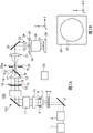
Fig. 1A is a diagram showing the configuration of an exposure apparatus 100 as one aspect of the present invention. Fig. 1B is a simplified cross-sectional view of the exposure apparatus 100. The exposure apparatus 100 is a lithography apparatus used in a manufacturing process of a semiconductor device or the like, which forms a pattern on a substrate. In the present embodiment, the exposure apparatus 100 is a step-and-scan exposure apparatus (scanner) that transfers a pattern of an original 25 onto a substrate 27 by exposing (scanning exposure) the substrate 27 while moving the original 25 and the substrate 27 in a scanning direction. However, the exposure apparatus 100 can employ a step-and-repeat (step-and-repeat) system or other exposure systems.
As shown in fig. 1A and 1B, an exposure apparatus 100 includes an illumination optical system 110 that irradiates an original 25 (reticle or mask) with light from a light source 1 and a projection optical system 26 that projects a pattern of the original 25 onto a substrate 27 (wafer, glass plate, or the like). The exposure apparatus 100 includes an original stage 29, a substrate stage 28, and a control unit 50. The substrate stage 28 has a function of moving in a first direction and a second direction orthogonal to each other in the substrate plane. In the present embodiment, as shown in fig. 1A and 1B, a coordinate system in which the first direction is the y direction (y axis), the second direction is the x direction (x axis), and the direction orthogonal to the first direction and the second direction is the z direction (z axis) is defined with the substrate stage 28 as a reference. The z direction is a direction corresponding to the optical axis direction of the projection optical system 26.
The light source 1 includes a mercury lamp having a wavelength of about 365nm, an excimer laser such as a KrF excimer laser having a wavelength of about 248nm and an ArF excimer laser having a wavelength of about 193 nm. The light source 1 emits light (exposure light) for irradiating the original 25.
The illumination optical system 110 includes a relay optical system 2, an exit angle holding optical element 5, a diffractive optical element 6, a condenser lens 7, a light shielding member 8, a prism unit 10, and a zoom lens unit 11. The illumination optical system 110 further includes an optical integrator 12, a diaphragm 13, a condenser lens 15, a light shielding unit 19, a masking unit 20, a condenser lens 21, and a collimator lens 23.
The relay optical system 2 is disposed between the light source 1 and the exit angle maintaining optical element 5. The relay optical system 2 guides the light from the light source 1 to the exit angle holding optical element 5. The exit angle maintaining optical element 5 is provided on the light source side of the diffractive optical element 6. The exit angle maintaining optical element 5 includes an optical integrator such as a fly-eye lens, a microlens array, and a fiber bundle. The exit angle maintaining optical element 5 guides the light from the light source 1 to the diffractive optical element 6 while maintaining the divergence angle constant. The emission angle maintaining optical element 5 reduces the influence of the output variation of the light source 1 on the light intensity distribution (pattern distribution) formed by the diffractive optical element 6.
The diffractive optical element 6 is disposed in a plane having a fourier transform relationship with the pupil plane 14 of the illumination optical system 110. The diffractive optical element 6 forms a desired light intensity distribution on the pupil plane 14 of the illumination optical system 110, which pupil plane 14 is a plane conjugate to the pupil plane of the projection optical system 26, or a plane conjugate to the pupil plane 14 of the illumination optical system 110 by converting the light intensity distribution of light from the light source 1 by a diffraction effect. The diffractive optical element 6 may be constituted by a Computer Generated Hologram (CGH) which is designed by a computer such that a desired diffraction pattern is obtained on a diffraction pattern plane. In the present embodiment, the light source shape formed on the pupil plane of the projection optical system 26 is referred to as an effective light source shape. The term "effective light source" refers to the light intensity distribution or light angle distribution in the illuminated plane and the plane conjugate to the illuminated plane. The diffractive optical element 6 is disposed between the exit angle maintaining optical element 5 and the condenser lens 7.
A plurality of diffractive optical elements 6 may be provided in the illumination optical system 110. For example, each of the plurality of diffractive optical elements 6 is attached to one of a plurality of grooves of a turntable (not shown). The diffractive optical elements 6 are formed in different effective light source shapes, respectively. These effective source shapes include small circles (relatively small circles), large circles (relatively large circles), donuts, dipoles, quadrupoles, and others. The method of illuminating the illuminated plane with an effective source shape of a ring, dipole or quadrupole is called modified illumination.
The light from the exit angle maintaining optical element 5 is diffracted by the diffractive optical element 6 and guided to the condenser lens 7. The condenser lens 7 is disposed between the diffractive optical element 6 and the prism unit 10. The condenser lens 7 condenses the light diffracted by the diffractive optical element 6, and forms a distribution pattern (light intensity distribution) in the fourier transform plane 9.
The fourier transform plane 9 is a plane that is located between the optical integrator 12 and the diffractive optical element 6 and has an optical fourier transform relationship with the diffractive optical element 6. By replacing the diffractive optical element 6 disposed in the optical path of the illumination optical system 110, the shape of the distribution pattern formed in the fourier transform plane 9 can be changed.
The light shielding member 8 is configured to be movable in a direction perpendicular to the optical axis 1b of the illumination optical system 110, and is disposed on the upstream side (light source side) of the fourier transform plane 9. The light shielding member 8 is disposed at a position slightly spaced (defocused) from the position of the fourier transform plane 9.
The prism unit 10 and the zoom lens unit 11 are disposed between the fourier transform plane 9 and the optical integrator 12. The prism unit 10 and the zoom lens unit 11 function as a zoom optical system that magnifies the light intensity distribution formed in the fourier transform plane 9. The prism unit 10 adjusts a ring ratio (annular ratio) or the like of the light intensity distribution formed in the fourier transform plane 9, and guides the light intensity distribution to the zoom lens unit 11. The zoom lens unit 11 is disposed between the prism unit 10 and the optical integrator 12. The zoom lens unit 11 includes, for example, a plurality of zoom lenses. The zoom lens unit 11 adjusts a σ value of the light intensity distribution formed in the fourier transform plane 9, which is obtained with reference to a ratio between a Numerical Aperture (NA) of the illumination optical system 110 and an NA of the projection optical system 26, and guides the light intensity distribution to the optical integrator 12.
The optical integrator 12 is disposed between the zoom lens unit 11 and the condenser lens 15. The optical integrator 12 includes a fly-eye lens that forms a large number of secondary light sources and guides the secondary light sources to the condenser lens 15 according to the light intensity distribution whose annular ratio, aperture angle, and σ value are adjusted. However, the optical integrator 12 may include another optical element, such as an optical tube, a diffractive optical element, and a microlens array, instead of the fly-eye lens. The optical integrator 12 uniformly irradiates the original 25 placed in the irradiated plane 24 with light that has passed through the diffractive optical element 6. The diaphragm 13 is disposed in the vicinity of the pupil plane 14 of the illumination optical system 110 between the optical integrator 12 and the condenser lens 15.
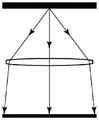
The condenser lens 15 is disposed between the optical integrator 12 and the original 25. Therefore, the condenser lens 15 can condense a large amount of light guided from the optical integrator 12 and irradiate the original 25 in a superimposed manner. When light rays are caused to enter the optical integrator 12 and are condensed by the condenser lens 15, a conjugate plane 20a as a focal plane of the condenser lens 15 is irradiated in a substantially rectangular shape.
The half mirror 16 is disposed on the rear side of the condenser lens 15. A part of the exposure light reflected on the half mirror 16 enters the light intensity measuring optical system 17. A sensor 18 that measures light intensity is disposed on the rear side of the light intensity measuring optical system 17. The exposure during which the exposure is performed is appropriately controlled according to the light intensity measured by the sensor 18.
The masking unit 20 including the X-blade and the Y-blade is disposed in a conjugate plane 20a, which conjugate plane 20a is a plane conjugate to the irradiated plane 24 and is irradiated with a substantially rectangular light intensity distribution. The mask unit 20 is disposed to define an illumination range of the original 25 (irradiated plane 24), and performs scanning in synchronization with the original stage 29 and the substrate stage 28. The original table 29 is a table that moves while holding the original 25. The substrate stage 28 is a stage that moves while holding the substrate 27.
The light shielding unit 19 is disposed at a position spaced (defocused) from the masking unit 20 (the conjugate plane 20a of the irradiated plane 24). Light reflected on a mirror 22 having a predetermined inclination with respect to the light beam from the condenser lens 21 illuminates an original 25 via a collimator lens 23.
The projection optical system 26 projects the pattern of the original 25 onto the substrate 27. Fig. 2 is a diagram schematically showing a cross section of the projection optical system 26. As shown in fig. 2, the projection optical system 26 includes a plurality of optical members (optical elements such as lenses and mirrors). An aperture stop 261 having a variable aperture is provided at the pupil plane 26a or in the vicinity of the pupil plane 26a of the projection optical system 26. By adjusting the aperture of the aperture stop 261, the NA of the projection optical system 26 can be set to a desired value. The resolution of the pattern image of the original 25 depends on the NA of the projection optical system 26 and the effective light source shape. Therefore, by appropriately setting (selecting) the NA of the projection optical system 26 and the effective light source shape, the resolution of the pattern of the original 25 can be improved.
As for the material of the optical member constituting the projection optical system 26, usable materials are limited depending on the wavelength of the exposure light to be emitted from the light source. When a mercury lamp having a wavelength of about 365nm is used as a light source, longitudinal chromatic aberration, lateral chromatic aberration, and the like can be favorably corrected by combining optical members made of about 10 materials. On the other hand, when excimer lasers such as KrF excimer lasers having a wavelength of about 248nm and ArF excimer lasers having a wavelength of about 193nm are used as light sources, materials that transmit exposure light from the excimer lasers are limited. In view of the optical transparency and cost of excimer lasers, the projection optical systems in the present state are usually made of quartz only. In this case, it is difficult to favorably correct chromatic aberration with the optical design of the projection optical system, and therefore the influence of chromatic aberration of the projection optical system is reduced by narrowing the wavelength spectral range of the laser light.
The description returns to fig. 1A and 1B. The control unit 50 is constituted by a computer (information processing apparatus) including a CPU, a memory, and the like. The control unit 50 operates the exposure apparatus 100 by generally controlling the units of the exposure apparatus 100 according to a program stored in the memory. The control unit 50 controls an exposure process of exposing the substrate 27 and various processes related to the exposure process. For example, in the present embodiment, the control unit 50 performs processing of determining an illumination shape (illumination light beam) for illumination in the pattern of the original 25.
In recent years, in a manufacturing process of a three-dimensional memory or an image pickup element, it is desired to form a penetration pattern having a thickness of several micrometers to several tens micrometers. In order to form such a thick penetration pattern with an exposure apparatus, it is desirable to enlarge the depth of focus of the projection optical system. As a technique for substantially enlarging the depth of focus, a method of performing multiple exposure while shifting the focal position in the optical axis direction of the projection optical system is known. As an example of multiple exposure, a focus latitude enhanced exposure (FLEX) method is known. In the FLEX method, for example, scanning exposure is performed while tilting the substrate with respect to the optical axis of the projection optical system so that dots in a region on the substrate are exposed in two or more defocused states. As another example of multiple exposure, resolution enhancement by a laser spectrum adjustment exposure (RELAX) method is known. In the RELAX method, the wavelength spectrum of the laser light source is adjusted to have light intensity peaks at a plurality of wavelengths.
Under the influence of optical characteristics including longitudinal chromatic aberration, coma aberration, and the like remaining in the projection optical system, light rays having different wavelengths respectively form images at different positions in the optical axis direction of the projection optical system. By adjusting the wavelength spectrum of the laser light source, the imaging position in the optical axis direction can be changed, thereby obtaining the effect of enlarging the focal depth.
In this way, in the RELAX method, the effect of enlarging the depth of focus is obtained by using the longitudinal chromatic aberration remaining in the projection optical system; however, aberrations such as lateral chromatic aberration and coma aberration remain in the projection optical system in addition to the longitudinal chromatic aberration, and these aberrations may cause a decrease in imaging performance.
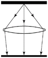
Fig. 3 is a schematic diagram showing an influence of lateral chromatic aberration of a projection optical system on imaging performance. Fig. 3 shows a state in which the illumination light beam having passed through the original 25 passes through the projection optical system 26 and reaches the substrate 27. In fig. 3, a beam 31 from an on-axis (on-axis) object point of original 25 and a beam 32 from an off-axis (off-axis) object point of original 25 are depicted. The beam 31 from the on-axis object point becomes a beam 33 converging at the on-axis image point and the beam 32 from the off-axis object point becomes a beam 35 converging at the off-axis image point.
Here, when the wavelength spectrum of the light beam from the original 25 includes a plurality of peaks, even for light beams emitted from the same object point, the imaging position varies depending on the wavelength. Here, it is assumed that the wavelength spectrum has a peak at a first wavelength and a peak at a second wavelength different from the first wavelength.
As for the light beam 31 from the on-axis object point, a light beam having a first wavelength (first illumination light) passes through the projection optical system 26 and becomes a light beam 33 and is condensed, and a light beam having a second wavelength (second illumination light) becomes a light beam 34 and is condensed under the influence of longitudinal chromatic aberration of the projection optical system 26. The imaging position of the light beam 33 in the optical axis direction and the imaging position of the light beam 34 in the optical axis direction are different from each other. For the on-axis light beam, there is little influence of lateral chromatic aberration, and therefore the imaging positions of the two differ only in the optical axis direction.
On the other hand, for the light beam 32 from the off-axis object point, the light beam having the first wavelength passes through the projection optical system 26 and becomes a light beam 35 and converges, and the light beam having the second wavelength becomes a light beam 36 and converges under the influence of the longitudinal chromatic aberration and the lateral chromatic aberration of the projection optical system 26. The imaging position of the light beam 35 and the imaging position of the light beam 36 are different from each other not only in the optical axis direction of the projection optical system 26 but also in a direction perpendicular to the optical axis direction. In other words, a positional deviation is generated between the pattern image formed by the light beam 35 (first illumination light) and the pattern image formed by the light beam 36 (second illumination light) in both the optical axis direction of the projection optical system 26 and the direction perpendicular to the optical axis direction.
As described above, for the off-axis light flux, the straight line connecting the condensing position of the first illumination light and the condensing position of the second illumination light is not perpendicular to the substrate 27. Therefore, a pattern image is formed obliquely with respect to the resist, with the result that an inclination occurs in the penetration pattern on the substrate 27. The inclination of the pattern image mainly occurs in proportion to the ratio T/L of the lateral chromatic aberration T and the longitudinal chromatic aberration L.
Since the positional deviation of the pattern image due to the lateral chromatic aberration is proportional to the distance between the image point and the optical axis, the inclination of the pattern image increases with the distance of the image point from the optical axis.
The pattern tilt due to the lateral chromatic aberration occurs in a direction in which the image is shifted by the lateral chromatic aberration. In other words, the inclination of the pattern occurs in the radiation direction with respect to the intersection between the image plane and the optical axis of the projection optical system 26. A step-and-scan exposure apparatus (scanner) performs exposure by scanning a slit-shaped exposure region. In other words, the region for exposure in the image plane of the projection optical system 26 has an elongated slit shape. Therefore, how the influence of the lateral chromatic aberration occurs, that is, how the inclination of the pattern occurs, varies depending on the direction of the pattern. Specifically, a tilt occurs in a pattern extending in the lateral direction with respect to the slit-shaped exposure area, and a tilt does not occur in a pattern extending in the longitudinal direction. Note that the inclination varies depending on the direction of the pattern. When the inclination of the pattern is greater than or equal to an allowable value, it may cause device defects, and the yield may be reduced.
In the present embodiment, in order to correct the inclination of the pattern image due to the positional deviation between the condensed position of the light beam of the first wavelength and the condensed position of the light beam of the second wavelength, the inclination of the illumination light beam is adjusted. Hereinafter, the operation of adjusting the inclination of the illumination light beam is referred to as telecentricity adjustment. Fig. 4 shows a state in which the light beam from the original 25 passes through the projection optical system 26 and reaches the substrate 27. In fig. 4, light rays 41, 42, 43 respectively represent principal rays of the illumination light beam that irradiates the original 25. The chief ray 41 illuminates an on-axis object point. The chief rays 42, 43 illuminate off-axis object points. The principal ray 43 travels as indicated by a ray 322 in the projection optical system 26, becomes a ray substantially perpendicular to the substrate 27, and reaches an image point. The principal ray 42 travels as indicated by the ray 321 in the projection optical system 26, becomes a ray inclined from the direction perpendicular to the substrate 27, and reaches an image point. In this way, by changing the inclination of the principal ray entering the original 25, the inclination of the light beam condensed on the substrate 27 can be adjusted, thereby obtaining the effect of inclining the pattern image. In other words, by appropriately controlling the inclination amount of the pattern image of the RELAX method and the inclination amount of the pattern image of the telecentric adjustment, the inclination of the pattern can be reduced.
Fig. 5A to 5C are diagrams illustrating reduction of the inclination of the pattern by telecentricity adjustment. Fig. 5A to 5C each show the shape of a pattern image to be formed by off-axis beams. These pattern images were obtained by simulation. The result was obtained by simulation under illumination conditions of NA =0.55, σ =0.50, the pattern having trenches with a diameter of 200nm, and the resist thickness being 4 μm. Here, σ is a value referring to a ratio between a Numerical Aperture (NA) of the illumination optical system 110 and an NA of the projection optical system 26.
Fig. 5A shows the result in the case where the telecentricity is not adjusted. Fig. 5B shows the result in the case where the telecentricity is adjusted to 0.05. Fig. 5C shows the result in the case where the telecentricity is adjusted to 0.10.
Here, adjusting the telecentricity by 0.05 means that the inclination of the illumination light beam is adjusted by θ = arctan0.05 when the inclination angle with respect to the optical axis direction of the projection optical system 26 is θ. As shown in fig. 5A to 5C, it appears that the inclination of the pattern decreases as the inclination of the illumination light beam increases.
Fig. 6 is a diagram showing a relationship between the inclination of the illumination light beam and the inclination of the pattern image. The inclination of the pattern image is described as the inclination of a straight line obtained by linear regression of the midpoints of the left and right walls of the pattern image. As the inclination of the illumination light beam increases, the inclination of the straight line decreases, and thus the inclination of the pattern image decreases. Here, the relationship between the inclination of the illumination light beam and the inclination of the pattern image is obtained by simulation. Alternatively, such a relationship may be obtained from the result of actual patterning.
The relationship between the inclination of the illumination light beam and the inclination of the pattern image varies depending on the pattern shape. This will be described with reference to fig. 7A to 7C. Fig. 7A to 7C each show a light intensity distribution formed by light beams from an off-axis object point in the original 25, and each show a light intensity distribution in a pupil plane of the projection optical system 26. Fig. 7A shows a light intensity distribution when exposure is performed by using a light beam having one peak in a wavelength spectrum. Reference numeral 54 denotes a pupil determined by an aperture stop of the projection optical system 26. Reference numeral 51 indicates the zero order diffracted beam from the off-axis object point. Reference numerals 52 and 53 denote positive first-order and negative first-order diffracted light beams formed from the illumination light beam diffracted by the pattern of the original 25, respectively.
In fig. 7A, the light intensity distribution of the zero-order diffracted light beam is located at the pupil center, and the shielding (eclipses) of the positive-order and negative-order diffracted light beams in the pupil peripheral area is also bilaterally symmetric, and therefore, even when defocusing occurs in the projection optical system 26, positional deviation of the pattern image hardly occurs in the image plane. In other words, the pattern image is hardly inclined.
Fig. 7B shows a light intensity distribution when the inclination of the illumination light beam is adjusted from the state of fig. 7A. Since the principal ray is caused to enter obliquely, the light intensity distribution 55 of the zero-order diffracted light beam in the pupil plane is shifted from the pupil center. Since the shading of the positive-first and negative-first order diffracted light beams 56, 57 in the pupil peripheral area is bilaterally asymmetric, the symmetry of the light intensity distribution in the pupil plane is reduced. Therefore, when defocus has occurred in the projection optical system 26, a positional deviation of the pattern image occurs in the image plane, and the pattern image is tilted.
The manner in which the diffracted light beams are generated changes depending on the shape of the pattern of the original 25 (e.g., the pattern pitch, the line-to-space ratio, the arrangement direction of the pattern in the line-and-space pattern), and the shading in the pupil peripheral area also changes. Therefore, the asymmetry of the light intensity distribution in the pupil plane also changes, and thus the center of mass of the light intensity also similarly changes. This means that in the case where defocus occurs in the projection optical system 26, a difference occurs in the amount of positional deviation of the pattern image in the image plane. Therefore, it appears that the ease of adjusting the inclination of the pattern differs depending on the pattern shape of the original 25.
Next, a method of adjusting the telecentricity of the illumination light beam will be described with reference to fig. 8A to 8C. Fig. 8A to 8C are simplified diagrams each showing a part of the illumination optical system 110. In fig. 8A to 8C, an optical path from the optical integrator 12 to a conjugate plane 20a as a plane conjugate to the original 25 is extracted and shown. The exit plane and the conjugate plane 20a of the optical integrator 12 have a relationship (fourier transform relationship) between an image and a pupil via the condenser lens 15.
Fig. 8A shows a reference state in which light emitted from one point of the optical integrator 12 enters the conjugate plane 20a substantially perpendicularly. In fig. 8A to 8C, the condenser lens 15 is drawn as a single lens, and is actually made of a plurality of lenses. By moving a part of the lenses constituting the condenser lens 15 for zoom magnification, the focal length of the entire condenser lens 15 can be changed. When the focal length of the condenser lens 15 is shortened as compared with the reference state, the off-axis light beam enters the conjugate plane 20a to approach the optical axis, as shown in fig. 8B. On the other hand, when the focal length of the condenser lens 15 is extended compared to the reference state, the off-axis light beam enters the conjugate plane 20a to move away from the optical axis, as shown in fig. 8C.
Since the conjugate plane 20a is a plane conjugate to the irradiated plane 24 (original 25), the light intensity distribution in the plane is the same as that in the irradiated plane 24 (original 25).
As described above, by changing the zoom magnification state of the lens included in the illumination optical system 110, the light intensity distribution in the irradiated plane 24 (original 25) can be adjusted. In other words, the inclination of the principal ray of the irradiation original 25 can also be adjusted. In this way, by continuously changing the focal length of the condenser lens 15 by the zoom mechanism, the tilt amount of the principal ray can also be continuously adjusted.
As shown in fig. 8A to 8C, the variation in the inclination of the light rays increases with the distance from the optical axis, and the inclination of the pattern image occurring due to the lateral chromatic aberration of the projection optical system 26 also increases with the distance from the optical axis. Therefore, in order to adjust the inclination of the pattern image due to the lateral chromatic aberration, a method of changing the zoom magnification state as shown in fig. 8A to 8C is suitable.
Next, a method of adjusting the inclination of the pattern image by controlling the aperture stop 261 of the projection optical system 26 will be described with reference to fig. 9. Fig. 9 shows a state in which the light beam from the original 25 passes through the projection optical system 26 and reaches the substrate 27. Reference numeral 811 denotes a principal ray of the light beam 81 that irradiates an on-axis object point. Reference numeral 82 denotes a light beam emitted from the off-axis object point and reaching the off-axis image point.
The principal ray 811 of beam 81 illuminating an on-axis object point and the principal ray 821 of beam 82 illuminating an off-axis object point enter original 25 substantially perpendicularly and also enter substrate 27 substantially perpendicularly. With respect to the marginal ray passing through the end of the aperture stop 261, the positive side marginal ray 822 and the negative side marginal ray 823 enter the substrate 27 at substantially the same incident angle. Therefore, the pattern image formed in the resist is hardly inclined.
Here, as shown in fig. 4, when the telecentricity is adjusted to correct the inclination of the pattern, the principal ray 831 of the light beam 82 illuminating the off-axis object point enters the original 25 in an oblique direction with respect to the optical axis, and also enters the substrate 27 in an oblique direction with respect to the optical axis. The optical path of the marginal ray is determined by moving the position of the aperture stop 261 from a to B and additionally changing the aperture of the aperture stop 261. As shown in fig. 9, the positive side edge light ray 832 and the negative side edge light ray 833 enter the substrate 27 at different angles from each other. By appropriately setting the position and the aperture of the aperture stop 261, the angle formed between the principal ray 831 and the positive-side marginal ray 832 and the angle formed between the principal ray 831 and the negative-side marginal ray 833 can be made substantially the same. By appropriately setting the optical path of the marginal ray in this way, the inclination of the pattern image can be controlled while maintaining the uniformity of the pattern image.
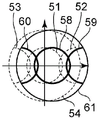
A light intensity distribution in a pupil plane of the projection optical system 26 when controlling the position and the aperture of the aperture stop 261 of the projection optical system 26 will be described with reference to fig. 7C. As in the case of fig. 7B, since the principal ray is obliquely entered, the light intensity distribution 58 of the zero-order diffracted light beam in the pupil plane is shifted from the pupil center. Since the position of the aperture stop 261 changes, the pupil area shifts from the area 54 to the area 61. As a result, the shading of the positive-first and negative-first order diffracted light beams 59, 60 in the pupil peripheral area is bilaterally symmetric with respect to the light intensity distribution of the zero-order diffracted light beam. When fig. 7A and 7C are compared with each other, the entire light intensity in the pupil plane has shifted, and the pattern formed in the resist is shifted in a direction perpendicular to the optical axis direction of the projection optical system 26.
Fig. 10A to 10D are diagrams illustrating that the inclination of the pattern image is reduced by adjusting the telecentricity and adjusting the aperture stop 261. Fig. 10A to 10D each show the shape of a pattern image to be formed by off-axis beams. These pattern images were obtained by simulation. The result was obtained by simulation under illumination conditions of NA =0.55, σ =0.50, the pattern having trenches with a diameter of 200nm, and the resist thickness being 4 μm. Fig. 10A shows the result in the case where the telecentricity and the aperture stop 261 are not adjusted. Fig. 10B shows the result in the case where the telecentricity is adjusted by 0.05 and the aperture stop 261 is adjusted accordingly. Fig. 10C shows the result in the case where the telecentricity is adjusted by 0.10 and the aperture stop 261 is adjusted accordingly. Fig. 10D shows the result in the case where the telecentricity is adjusted by 0.15 and the aperture stop 261 is adjusted accordingly.
It appears that the inclination of the pattern decreases with increasing inclination of the illumination beam.
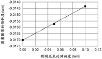
Fig. 11 is a diagram showing a relationship between the inclination of the illumination light beam and the inclination of the pattern image. The inclination of the pattern image is described as the inclination of a straight line obtained by linear regression of the midpoints of the left and right walls of the pattern image. As the inclination of the illumination light beam increases, the inclination of the straight line decreases, and thus the inclination of the pattern image decreases. Here, the relationship between the inclination of the illumination light beam and the inclination of the pattern image is obtained by simulation. Alternatively, such a relationship may be obtained from the result of actual patterning.
As described above, with the exposure apparatus of the present embodiment, by appropriately setting the inclination of the illumination light beam that illuminates the pattern, the inclination of the pattern image formed in the resist film can be effectively reduced.
Modifications of the invention
In fig. 9, the position of the aperture stop 261 is changed. Alternatively, it is also possible to prepare a plurality of aperture stops, and dispose aperture stops whose apertures are variable at the position a and the position B, respectively. When the light beam is caused to enter the original 25 substantially perpendicularly, the diameter of the aperture stop disposed at the position B is increased to prevent shading in the light, and the diameter of the aperture stop disposed at the position a is appropriately set. When the light beam is caused to obliquely enter the original 25, the diameter of the aperture stop disposed at the position a is increased to prevent shading in the light, and the diameter of the aperture stop disposed at the position B is appropriately set.
Exposure mode in exposure apparatus
Manufacturing processes for semiconductor devices such as memories and image pickup elements include a process of forming a pattern layer on a substrate. In this process, a pattern image is formed in the resist by using an exposure apparatus, and a pattern layer including trenches is formed by etching or the like. The thickness of the resist used may differ depending on the pattern layer to be formed, and the depth of focus used in the projection optical system of the exposure apparatus also differs depending on the thickness of the resist. When the thickness of the resist is thick, pattern formation can be performed by multiple exposure by the RELAX method or the like. In the RELAX method, it is necessary to control the oscillation state of the laser light source so as to have light intensity peaks at a plurality of wavelengths. On the other hand, when the thickness of the resist is thin, the oscillation state of the laser light source is controlled to have a light intensity peak at a single wavelength.
In this way, since the depth of focus or the like of the projection optical system needs to be changed for each layer to be formed on the substrate, the exposure mode in the exposure apparatus can be switched as needed. For example, it is conceivable to switch the oscillation state of the laser light source according to the exposure mode. In order to switch the oscillation state of the laser light source, a mechanism capable of switching the oscillation state is provided in the light source. The exposure apparatus can switch the oscillation state of the laser light source according to a recipe for setting various parameters during execution of exposure.
For example, the exposure mode can be switched between a first mode and a second mode. The first mode is a mode in which exposure is performed by controlling the oscillation state of the laser light source to have a light intensity peak at a single wavelength (reference wavelength). The second mode is a mode in which exposure is performed with illumination light including first illumination light having a first wavelength different from the reference wavelength and second illumination light having a second wavelength different from the reference wavelength or the first wavelength. By changing the incident angle of the off-axis light beam to the original in the second mode and the incident angle of the off-axis light beam to the original in the first mode, the occurrence of the inclination of the pattern image in the second mode can be reduced.
When exposure based on the RELAX method is performed in the second mode, values of a plurality of wavelengths corresponding to light intensity peaks and wavelength differences are specified, and thus these parameters can be set as one of the setting items of the recipe. In order to adjust the inclination of the illumination beam and the aperture stop for exposure based on the RELAX method, the exposure apparatus may be configured to automatically perform adjustment by using a recipe, or a user may be required to determine whether to perform adjustment. When the exposure apparatus automatically performs adjustment, the adjustment amount is determined in consideration of the feature of the pattern, the telecentricity of the illumination beam, and the like. At this time, the exposure apparatus may be configured to be able to acquire information on the characteristics of the pattern of the original.
Method for manufacturing product
A method of manufacturing a semiconductor device (a memory or a photoelectric conversion device such as an image pickup element) by using the exposure apparatus typical in the present embodiment will be described. The exposure apparatus of the present embodiment is suitable for a manufacturing method for a semiconductor device including thick film processing. A process of forming the pixel separating section in the image pickup element (light source conversion device) is an example of a thick film process.
Hereinafter, a process of forming the pixel separation portion in the manufacturing process of the image pickup element will be described with reference to fig. 12. In step S101, a semiconductor substrate 101 having a first surface S1 and a second surface S2 as mutually opposed surfaces is prepared. The semiconductor substrate 101 is typically a silicon substrate or a silicon layer. Subsequently, in step S102, an insulating film (e.g., a silicon oxide film) 102 is formed on the first surface S1 of the semiconductor substrate 101.
Subsequently, in step S103, a resist 103 is applied on the first surface S1 of the semiconductor substrate 101, more specifically, on the insulating film 102 on the first surface S1 of the semiconductor substrate 101. Further, in step S104, as described in the above-described embodiment, by performing an exposure operation in a state where the inclination of the illumination light beam is adjusted, a pattern image is formed in the resist 103, and a groove (trench) 104 is formed by etching or the like. By reducing the inclination of the pattern image to be formed in the resist 103, the groove 104 having the reduced inclination can be formed.
Subsequently, in step S105, the groove 105 is formed on the first surface S1 of the semiconductor substrate 101 by etching the semiconductor substrate 101 by a dry etching method or the like. In order to protect the first surface S1 of the semiconductor substrate 101 in this etching, it is desirable to coat the resist 103 thickly.
Subsequently, in step S106, the resist 103 is removed, and then the gettering region 106 is formed by implanting ions into the semiconductor substrate 101 via the groove 105. In other words, in step S106, ions are implanted into the semiconductor substrate 101 through the groove 105 in a state where the region of the first surface S1 of the semiconductor substrate 101 other than the region where the groove 105 exists is masked with the insulating film 102. Each gettering region 106 may include a first portion located below the bottom of the groove 105 and a second portion located at the side of the groove 105. In an example, the concentration of the group 14 element in the first portion is higher than the concentration of the group 14 element in the second portion. When the semiconductor substrate 101 is a silicon substrate, the ions may be ions of a group 14 element other than silicon. Ion implantation equipment is used to implant ions. The acceleration energy of the implanted ions can be determined so that the ions do not penetrate the insulating film 102 as a hard mask and reach the semiconductor substrate 101. For example, in the case where the thickness of the insulating film 102 is 300nm when ions are implanted, the ions hardly penetrate the insulating film 102 at an acceleration energy of about 20 keV.
When the semiconductor substrate 101 is a silicon substrate, a material which is a component of ions to be implanted into the semiconductor substrate 101 in step S106 is suitably carbon. Alternatively, a hydrocarbon that is a molecule containing carbon may be employed. When the semiconductor substrate 101 is a silicon substrate, a material which is a component of ions to be implanted into the semiconductor substrate 101 in step S106 may be germanium, tin, or lead. By implanting ions of carbon, germanium, tin, or lead into a silicon substrate serving as the semiconductor substrate 101, it is possible to impart local strain in the silicon substrate and make the silicon substrate serve as a gettering site. By implanting ions into the semiconductor substrate 101 via the grooves 105, the gettering region 106 can be formed at a deep position of the semiconductor substrate 101 even with a relatively low acceleration energy.
Subsequently, in step S107, the insulating film 102 is removed. In step S108, an insulating film (e.g., a silicon nitride film) 107 is formed in the groove 105 and on the first surface S1 of the semiconductor substrate 101 by a film forming method (e.g., low-pressure CVD or the like) so that an insulator is disposed or filled in the groove 105. Subsequently, in step S109, a part of the insulating film 107 present on the first surface S1 of the semiconductor substrate 101 is removed by CMP or the like. Therefore, a part of the insulating film 107 existing in the groove 105 remains as the pixel separating portion 108 disposed or filled in the groove 105.
Step S108 and step S109 are not necessarily performed. When step S108 and step S109 are not performed, the groove 105 remains as an air gap, and the air gap can be used as a pixel separating portion. The pixel separating portion 108 disposed in each groove 105 need not completely fill the groove 105, and an air gap may exist in the groove 105. The pixel separating portion 108 may be constituted only of an insulator, and may also be a combined structure of an insulator and a non-insulator (semiconductor or conductor). In this case, in order to avoid contact between the non-insulator and the semiconductor substrate 101, an insulator may be disposed between the non-insulator and the semiconductor substrate 101.
As described above, the pixel separating portion 108 is formed by the first forming step of forming the groove 105 in the semiconductor substrate 101 and the second forming step of forming the pixel separating portion 108 in the groove 105. After that, a charge storage region, a gate electrode, and the like are formed in a region between the plurality of pixel separating portions, thereby making an image pickup element.
While the present invention has been described with reference to the embodiments, it is to be understood that the invention is not limited to the disclosed embodiments, but is instead defined by the scope of the appended claims.
Claims (16)
1. An exposure apparatus that exposes a substrate by using an original in which a pattern is formed, the exposure apparatus comprising:
an illumination optical system arranged to guide illumination light to the original, the illumination light including first illumination light having a first wavelength and second illumination light having a second wavelength different from the first wavelength; and
a projection optical system arranged to form pattern images of the original by using the illumination light at a plurality of positions in an optical axis direction of the projection optical system, wherein
The illumination optical system is configured to adjust a positional deviation between a pattern image formed by the first illumination light and a pattern image formed by the second illumination light in a direction perpendicular to the optical axis direction by changing an incident angle of the illumination light entering the original.
2. The exposure apparatus according to claim 1, wherein the illumination optical system is configured to change an incident angle in accordance with an optical characteristic of the projection optical system.
3. The exposure apparatus according to claim 2, wherein the optical characteristic is a lateral chromatic aberration.
4. The exposure apparatus according to claim 2, wherein the optical characteristic is coma aberration.
5. The exposure apparatus according to claim 3, wherein an incident angle is changed to reduce a positional deviation due to a lateral chromatic aberration of the projection optical system.
6. The exposure apparatus according to claim 4, wherein an incident angle is changed to reduce a positional deviation due to coma aberration of the projection optical system.
7. The exposure apparatus according to claim 1, wherein the pattern is a line interval pattern, and the positional deviation is a positional deviation that occurs in an arrangement direction of the pattern.
8. The exposure apparatus according to claim 1, wherein an incident angle is controlled by changing a position of an optical element included in the illumination optical system.
9. The exposure apparatus according to claim 1, wherein an aperture stop is included in the projection optical system, and an incident angle of light irradiating the substrate is changed by changing at least one of a position of the aperture stop and a size of an aperture.
10. The exposure apparatus according to any one of claims 1 to 9, wherein each of the first illumination light and the second illumination light is light shifted in wavelength with respect to light having a reference wavelength oscillated from the light source.
11. The exposure apparatus according to claim 10, wherein the wavelength of the first illumination light and the wavelength of the second illumination light are determined in accordance with a shape of the pattern.
12. An exposure apparatus that exposes a substrate by using an original in which a pattern is formed, and is capable of switching between a first mode and a second mode, wherein the first mode performs exposure by using illumination light having a reference wavelength, and the second mode performs exposure by using illumination light including first illumination light having a first wavelength different from the reference wavelength and second illumination light having a second wavelength different from the reference wavelength or the first wavelength, wherein the exposure apparatus performs exposure by using illumination light including first illumination light having a first wavelength different from the reference wavelength and second illumination light having a second wavelength different from the reference wavelength or the first wavelength
The apparatus is configured such that an incident angle of illumination light having a reference wavelength entering the original in the first mode is different from an incident angle of second illumination light entering the original in the second mode.
13. The exposure apparatus according to claim 12 wherein the incident angle of the illumination light with the reference wavelength entering the original in the first mode is made different from the incident angle of the second illumination light entering the original in the second mode by changing the incident angle of the second illumination light in the second mode.
14. An exposure method of exposing a substrate by using an original in which a pattern is formed, the exposure method comprising the steps of:
illuminating an original with illumination light including first illumination light having a first wavelength and second illumination light having a second wavelength different from the first wavelength;
forming a pattern image of an original by using the illumination light at a plurality of positions in an optical axis direction of the projection optical system using the projection optical system;
the incident angle of the illumination light entering the original is adjusted to reduce a positional deviation between the pattern image formed by the first illumination light and the pattern image formed by the second illumination light in a direction perpendicular to the optical axis direction.
15. A manufacturing method of a semiconductor device, the manufacturing method comprising: a first forming step of forming a groove in a substrate using the exposure method according to claim 14; and a second forming step of forming a pixel separating portion in the groove.
16. A computer program which, when run on a computer, causes the computer to control an exposure apparatus to perform an exposure method according to claim 14.
Applications Claiming Priority (2)
| Application Number | Priority Date | Filing Date | Title |
|---|---|---|---|
| JP2021104157A JP2023003153A (en) | 2021-06-23 | 2021-06-23 | Exposure apparatus, exposure method, and manufacturing method for product |
| JP2021-104157 | 2021-06-23 |
Publications (1)
| Publication Number | Publication Date |
|---|---|
| CN115509091A true CN115509091A (en) | 2022-12-23 |
Family
ID=82117158
Family Applications (1)
| Application Number | Title | Priority Date | Filing Date |
|---|---|---|---|
| CN202210717284.0A Pending CN115509091A (en) | 2021-06-23 | 2022-06-23 | Exposure apparatus, exposure method, and method for manufacturing product |
Country Status (6)
| Country | Link |
|---|---|
| US (2) | US11835863B2 (en) |
| EP (1) | EP4109179A3 (en) |
| JP (1) | JP2023003153A (en) |
| KR (1) | KR20220170754A (en) |
| CN (1) | CN115509091A (en) |
| TW (1) | TW202301038A (en) |
Family Cites Families (11)
| Publication number | Priority date | Publication date | Assignee | Title |
|---|---|---|---|---|
| JPH0669014B2 (en) * | 1986-02-24 | 1994-08-31 | 株式会社ニコン | Exposure equipment |
| JP2619473B2 (en) | 1987-06-17 | 1997-06-11 | 株式会社日立製作所 | Reduction projection exposure method |
| US6885433B2 (en) * | 1990-11-15 | 2005-04-26 | Nikon Corporation | Projection exposure apparatus and method |
| US6078380A (en) * | 1991-10-08 | 2000-06-20 | Nikon Corporation | Projection exposure apparatus and method involving variation and correction of light intensity distributions, detection and control of imaging characteristics, and control of exposure |
| JP2001217174A (en) * | 2000-02-01 | 2001-08-10 | Nikon Corp | Position detection method, position detection device, exposure method and aligner |
| WO2003021352A1 (en) * | 2001-08-31 | 2003-03-13 | Canon Kabushiki Kaisha | Reticle and optical characteristic measuring method |
| US7262110B2 (en) * | 2004-08-23 | 2007-08-28 | Micron Technology, Inc. | Trench isolation structure and method of formation |
| EP2109143B1 (en) * | 2008-04-09 | 2013-05-29 | Sony Corporation | Solid-state imaging device, production method thereof, and electronic device |
| JP2014179446A (en) * | 2013-03-14 | 2014-09-25 | Sharp Corp | Semiconductor imaging device and manufacturing method therefor |
| JP6567005B2 (en) * | 2017-08-31 | 2019-08-28 | キヤノン株式会社 | Exposure apparatus, adjustment method, and article manufacturing method |
| JPWO2019146448A1 (en) * | 2018-01-24 | 2021-01-07 | 株式会社ニコン | Exposure device and exposure method |
-
2021
- 2021-06-23 JP JP2021104157A patent/JP2023003153A/en active Pending
-
2022
- 2022-06-09 TW TW111121379A patent/TW202301038A/en unknown
- 2022-06-15 KR KR1020220072669A patent/KR20220170754A/en active Search and Examination
- 2022-06-20 EP EP22179902.6A patent/EP4109179A3/en active Pending
- 2022-06-22 US US17/847,037 patent/US11835863B2/en active Active
- 2022-06-23 CN CN202210717284.0A patent/CN115509091A/en active Pending
-
2023
- 2023-11-01 US US18/499,883 patent/US20240077806A1/en active Pending
Also Published As
| Publication number | Publication date |
|---|---|
| US11835863B2 (en) | 2023-12-05 |
| EP4109179A3 (en) | 2023-01-04 |
| US20220413392A1 (en) | 2022-12-29 |
| JP2023003153A (en) | 2023-01-11 |
| US20240077806A1 (en) | 2024-03-07 |
| TW202301038A (en) | 2023-01-01 |
| EP4109179A2 (en) | 2022-12-28 |
| KR20220170754A (en) | 2022-12-30 |
Similar Documents
| Publication | Publication Date | Title |
|---|---|---|
| US10976668B2 (en) | Illumination optical unit and optical system for EUV projection lithography | |
| JP3631094B2 (en) | Projection exposure apparatus and device manufacturing method | |
| JPH1154426A (en) | Lighting device and aligner using the same | |
| KR100485314B1 (en) | Projection exposure apparatus and device manufacturing method using the same | |
| KR20080056094A (en) | Exposure apparatus and device fabrication method | |
| KR100823405B1 (en) | Exposure apparatus and device manufacturing method | |
| KR100819240B1 (en) | Measuring apparatus of effective light source distribution of illumination optical system of exposure apparatus and exposure apparatus having the same | |
| JP3605047B2 (en) | Illumination apparatus, exposure apparatus, device manufacturing method and device | |
| JPH0737774A (en) | Scanning aligner | |
| JP4684563B2 (en) | Exposure apparatus and method | |
| JP2008124308A (en) | Exposure method and exposure apparatus, and device manufacturing method using the same | |
| US11835863B2 (en) | Exposure apparatus, exposure method, and manufacturing method for product | |
| JP4838430B2 (en) | Exposure apparatus and device manufacturing method | |
| US20220171291A1 (en) | Exposure apparatus and method of manufacturing article | |
| CN114365045B (en) | Exposure apparatus and method for manufacturing article | |
| JP4950795B2 (en) | Exposure apparatus, device manufacturing method, and correction method | |
| US11656554B2 (en) | Exposure apparatus, exposure method, and method of manufacturing article | |
| JP7336922B2 (en) | Exposure apparatus and article manufacturing method | |
| JP2023048535A (en) | Exposure apparatus, exposure method, and manufacturing method for semiconductor device | |
| JP7446068B2 (en) | Exposure apparatus and article manufacturing method | |
| JP2009099879A (en) | Illumination optical system, exposure device, and device manufacturing method | |
| JP2008277347A (en) | Exposure equipment and process for fabricating device |
Legal Events
| Date | Code | Title | Description |
|---|---|---|---|
| PB01 | Publication | ||
| PB01 | Publication | ||
| SE01 | Entry into force of request for substantive examination | ||
| SE01 | Entry into force of request for substantive examination |