KR20220170754A - Exposure apparatus, exposure method, and manufacturing method for product - Google Patents
Exposure apparatus, exposure method, and manufacturing method for product Download PDFInfo
- Publication number
- KR20220170754A KR20220170754A KR1020220072669A KR20220072669A KR20220170754A KR 20220170754 A KR20220170754 A KR 20220170754A KR 1020220072669 A KR1020220072669 A KR 1020220072669A KR 20220072669 A KR20220072669 A KR 20220072669A KR 20220170754 A KR20220170754 A KR 20220170754A
- Authority
- KR
- South Korea
- Prior art keywords
- illumination light
- pattern
- optical system
- wavelength
- original plate
- Prior art date
Links
- 238000000034 method Methods 0.000 title claims description 46
- 238000004519 manufacturing process Methods 0.000 title claims description 12
- 230000003287 optical effect Effects 0.000 claims abstract description 197
- 238000005286 illumination Methods 0.000 claims abstract description 111
- 239000000758 substrate Substances 0.000 claims abstract description 75
- 239000004065 semiconductor Substances 0.000 claims description 33
- 230000004075 alteration Effects 0.000 claims description 27
- 230000015572 biosynthetic process Effects 0.000 claims description 6
- 206010010071 Coma Diseases 0.000 claims description 3
- 230000008859 change Effects 0.000 claims description 3
- 238000004590 computer program Methods 0.000 claims description 2
- 230000004907 flux Effects 0.000 description 64
- 238000009826 distribution Methods 0.000 description 29
- 210000001747 pupil Anatomy 0.000 description 22
- 238000010586 diagram Methods 0.000 description 16
- 230000008569 process Effects 0.000 description 12
- 150000002500 ions Chemical class 0.000 description 11
- 238000003384 imaging method Methods 0.000 description 10
- XUIMIQQOPSSXEZ-UHFFFAOYSA-N Silicon Chemical compound [Si] XUIMIQQOPSSXEZ-UHFFFAOYSA-N 0.000 description 9
- 229910052710 silicon Inorganic materials 0.000 description 9
- 239000010703 silicon Substances 0.000 description 9
- 239000012212 insulator Substances 0.000 description 7
- 230000010355 oscillation Effects 0.000 description 7
- 230000007423 decrease Effects 0.000 description 6
- 230000000694 effects Effects 0.000 description 6
- 239000000463 material Substances 0.000 description 6
- 230000002093 peripheral effect Effects 0.000 description 6
- 238000004088 simulation Methods 0.000 description 6
- 238000001228 spectrum Methods 0.000 description 6
- 230000000903 blocking effect Effects 0.000 description 5
- 238000004321 preservation Methods 0.000 description 5
- 230000006870 function Effects 0.000 description 4
- 238000005247 gettering Methods 0.000 description 4
- 230000000873 masking effect Effects 0.000 description 4
- 230000007261 regionalization Effects 0.000 description 4
- OKTJSMMVPCPJKN-UHFFFAOYSA-N Carbon Chemical compound [C] OKTJSMMVPCPJKN-UHFFFAOYSA-N 0.000 description 3
- 230000001133 acceleration Effects 0.000 description 3
- 229910052799 carbon Inorganic materials 0.000 description 3
- 229910052800 carbon group element Inorganic materials 0.000 description 3
- 238000005530 etching Methods 0.000 description 3
- 238000005468 ion implantation Methods 0.000 description 3
- VYPSYNLAJGMNEJ-UHFFFAOYSA-N silicon dioxide Inorganic materials O=[Si]=O VYPSYNLAJGMNEJ-UHFFFAOYSA-N 0.000 description 3
- ATJFFYVFTNAWJD-UHFFFAOYSA-N Tin Chemical compound [Sn] ATJFFYVFTNAWJD-UHFFFAOYSA-N 0.000 description 2
- 238000006243 chemical reaction Methods 0.000 description 2
- 229910052732 germanium Inorganic materials 0.000 description 2
- GNPVGFCGXDBREM-UHFFFAOYSA-N germanium atom Chemical compound [Ge] GNPVGFCGXDBREM-UHFFFAOYSA-N 0.000 description 2
- 238000012417 linear regression Methods 0.000 description 2
- 230000007246 mechanism Effects 0.000 description 2
- QSHDDOUJBYECFT-UHFFFAOYSA-N mercury Chemical compound [Hg] QSHDDOUJBYECFT-UHFFFAOYSA-N 0.000 description 2
- 229910052753 mercury Inorganic materials 0.000 description 2
- 229910052718 tin Inorganic materials 0.000 description 2
- 229910052581 Si3N4 Inorganic materials 0.000 description 1
- 230000009471 action Effects 0.000 description 1
- 238000013459 approach Methods 0.000 description 1
- 239000004020 conductor Substances 0.000 description 1
- 230000007547 defect Effects 0.000 description 1
- 238000013461 design Methods 0.000 description 1
- 230000006866 deterioration Effects 0.000 description 1
- 238000001312 dry etching Methods 0.000 description 1
- 239000000835 fiber Substances 0.000 description 1
- 239000011521 glass Substances 0.000 description 1
- 229930195733 hydrocarbon Natural products 0.000 description 1
- 150000002430 hydrocarbons Chemical class 0.000 description 1
- 230000010365 information processing Effects 0.000 description 1
- 238000001459 lithography Methods 0.000 description 1
- 239000010453 quartz Substances 0.000 description 1
- 238000000926 separation method Methods 0.000 description 1
- HQVNEWCFYHHQES-UHFFFAOYSA-N silicon nitride Chemical compound N12[Si]34N5[Si]62N3[Si]51N64 HQVNEWCFYHHQES-UHFFFAOYSA-N 0.000 description 1
- 229910052814 silicon oxide Inorganic materials 0.000 description 1
- 238000003860 storage Methods 0.000 description 1
- 238000002834 transmittance Methods 0.000 description 1
- 238000011144 upstream manufacturing Methods 0.000 description 1
- 239000011800 void material Substances 0.000 description 1
Images


Classifications
-
- G—PHYSICS
- G03—PHOTOGRAPHY; CINEMATOGRAPHY; ANALOGOUS TECHNIQUES USING WAVES OTHER THAN OPTICAL WAVES; ELECTROGRAPHY; HOLOGRAPHY
- G03F—PHOTOMECHANICAL PRODUCTION OF TEXTURED OR PATTERNED SURFACES, e.g. FOR PRINTING, FOR PROCESSING OF SEMICONDUCTOR DEVICES; MATERIALS THEREFOR; ORIGINALS THEREFOR; APPARATUS SPECIALLY ADAPTED THEREFOR
- G03F7/00—Photomechanical, e.g. photolithographic, production of textured or patterned surfaces, e.g. printing surfaces; Materials therefor, e.g. comprising photoresists; Apparatus specially adapted therefor
- G03F7/70—Microphotolithographic exposure; Apparatus therefor
- G03F7/70058—Mask illumination systems
- G03F7/70091—Illumination settings, i.e. intensity distribution in the pupil plane or angular distribution in the field plane; On-axis or off-axis settings, e.g. annular, dipole or quadrupole settings; Partial coherence control, i.e. sigma or numerical aperture [NA]
-
- G—PHYSICS
- G03—PHOTOGRAPHY; CINEMATOGRAPHY; ANALOGOUS TECHNIQUES USING WAVES OTHER THAN OPTICAL WAVES; ELECTROGRAPHY; HOLOGRAPHY
- G03F—PHOTOMECHANICAL PRODUCTION OF TEXTURED OR PATTERNED SURFACES, e.g. FOR PRINTING, FOR PROCESSING OF SEMICONDUCTOR DEVICES; MATERIALS THEREFOR; ORIGINALS THEREFOR; APPARATUS SPECIALLY ADAPTED THEREFOR
- G03F7/00—Photomechanical, e.g. photolithographic, production of textured or patterned surfaces, e.g. printing surfaces; Materials therefor, e.g. comprising photoresists; Apparatus specially adapted therefor
- G03F7/70—Microphotolithographic exposure; Apparatus therefor
- G03F7/70216—Mask projection systems
- G03F7/70308—Optical correction elements, filters or phase plates for manipulating imaging light, e.g. intensity, wavelength, polarisation, phase or image shift
-
- G—PHYSICS
- G03—PHOTOGRAPHY; CINEMATOGRAPHY; ANALOGOUS TECHNIQUES USING WAVES OTHER THAN OPTICAL WAVES; ELECTROGRAPHY; HOLOGRAPHY
- G03F—PHOTOMECHANICAL PRODUCTION OF TEXTURED OR PATTERNED SURFACES, e.g. FOR PRINTING, FOR PROCESSING OF SEMICONDUCTOR DEVICES; MATERIALS THEREFOR; ORIGINALS THEREFOR; APPARATUS SPECIALLY ADAPTED THEREFOR
- G03F7/00—Photomechanical, e.g. photolithographic, production of textured or patterned surfaces, e.g. printing surfaces; Materials therefor, e.g. comprising photoresists; Apparatus specially adapted therefor
- G03F7/70—Microphotolithographic exposure; Apparatus therefor
- G03F7/70483—Information management; Active and passive control; Testing; Wafer monitoring, e.g. pattern monitoring
- G03F7/70591—Testing optical components
- G03F7/706—Aberration measurement
-
- G—PHYSICS
- G01—MEASURING; TESTING
- G01M—TESTING STATIC OR DYNAMIC BALANCE OF MACHINES OR STRUCTURES; TESTING OF STRUCTURES OR APPARATUS, NOT OTHERWISE PROVIDED FOR
- G01M11/00—Testing of optical apparatus; Testing structures by optical methods not otherwise provided for
- G01M11/02—Testing optical properties
- G01M11/0221—Testing optical properties by determining the optical axis or position of lenses
-
- G—PHYSICS
- G01—MEASURING; TESTING
- G01M—TESTING STATIC OR DYNAMIC BALANCE OF MACHINES OR STRUCTURES; TESTING OF STRUCTURES OR APPARATUS, NOT OTHERWISE PROVIDED FOR
- G01M11/00—Testing of optical apparatus; Testing structures by optical methods not otherwise provided for
- G01M11/02—Testing optical properties
- G01M11/0242—Testing optical properties by measuring geometrical properties or aberrations
- G01M11/0257—Testing optical properties by measuring geometrical properties or aberrations by analyzing the image formed by the object to be tested
- G01M11/0264—Testing optical properties by measuring geometrical properties or aberrations by analyzing the image formed by the object to be tested by using targets or reference patterns
-
- G—PHYSICS
- G02—OPTICS
- G02B—OPTICAL ELEMENTS, SYSTEMS OR APPARATUS
- G02B7/00—Mountings, adjusting means, or light-tight connections, for optical elements
- G02B7/003—Alignment of optical elements
-
- G—PHYSICS
- G03—PHOTOGRAPHY; CINEMATOGRAPHY; ANALOGOUS TECHNIQUES USING WAVES OTHER THAN OPTICAL WAVES; ELECTROGRAPHY; HOLOGRAPHY
- G03F—PHOTOMECHANICAL PRODUCTION OF TEXTURED OR PATTERNED SURFACES, e.g. FOR PRINTING, FOR PROCESSING OF SEMICONDUCTOR DEVICES; MATERIALS THEREFOR; ORIGINALS THEREFOR; APPARATUS SPECIALLY ADAPTED THEREFOR
- G03F7/00—Photomechanical, e.g. photolithographic, production of textured or patterned surfaces, e.g. printing surfaces; Materials therefor, e.g. comprising photoresists; Apparatus specially adapted therefor
- G03F7/70—Microphotolithographic exposure; Apparatus therefor
- G03F7/70008—Production of exposure light, i.e. light sources
-
- G—PHYSICS
- G03—PHOTOGRAPHY; CINEMATOGRAPHY; ANALOGOUS TECHNIQUES USING WAVES OTHER THAN OPTICAL WAVES; ELECTROGRAPHY; HOLOGRAPHY
- G03F—PHOTOMECHANICAL PRODUCTION OF TEXTURED OR PATTERNED SURFACES, e.g. FOR PRINTING, FOR PROCESSING OF SEMICONDUCTOR DEVICES; MATERIALS THEREFOR; ORIGINALS THEREFOR; APPARATUS SPECIALLY ADAPTED THEREFOR
- G03F7/00—Photomechanical, e.g. photolithographic, production of textured or patterned surfaces, e.g. printing surfaces; Materials therefor, e.g. comprising photoresists; Apparatus specially adapted therefor
- G03F7/70—Microphotolithographic exposure; Apparatus therefor
- G03F7/70058—Mask illumination systems
- G03F7/70091—Illumination settings, i.e. intensity distribution in the pupil plane or angular distribution in the field plane; On-axis or off-axis settings, e.g. annular, dipole or quadrupole settings; Partial coherence control, i.e. sigma or numerical aperture [NA]
- G03F7/70108—Off-axis setting using a light-guiding element, e.g. diffractive optical elements [DOEs] or light guides
-
- G—PHYSICS
- G03—PHOTOGRAPHY; CINEMATOGRAPHY; ANALOGOUS TECHNIQUES USING WAVES OTHER THAN OPTICAL WAVES; ELECTROGRAPHY; HOLOGRAPHY
- G03F—PHOTOMECHANICAL PRODUCTION OF TEXTURED OR PATTERNED SURFACES, e.g. FOR PRINTING, FOR PROCESSING OF SEMICONDUCTOR DEVICES; MATERIALS THEREFOR; ORIGINALS THEREFOR; APPARATUS SPECIALLY ADAPTED THEREFOR
- G03F7/00—Photomechanical, e.g. photolithographic, production of textured or patterned surfaces, e.g. printing surfaces; Materials therefor, e.g. comprising photoresists; Apparatus specially adapted therefor
- G03F7/70—Microphotolithographic exposure; Apparatus therefor
- G03F7/70058—Mask illumination systems
- G03F7/7015—Details of optical elements
- G03F7/70158—Diffractive optical elements
-
- G—PHYSICS
- G03—PHOTOGRAPHY; CINEMATOGRAPHY; ANALOGOUS TECHNIQUES USING WAVES OTHER THAN OPTICAL WAVES; ELECTROGRAPHY; HOLOGRAPHY
- G03F—PHOTOMECHANICAL PRODUCTION OF TEXTURED OR PATTERNED SURFACES, e.g. FOR PRINTING, FOR PROCESSING OF SEMICONDUCTOR DEVICES; MATERIALS THEREFOR; ORIGINALS THEREFOR; APPARATUS SPECIALLY ADAPTED THEREFOR
- G03F7/00—Photomechanical, e.g. photolithographic, production of textured or patterned surfaces, e.g. printing surfaces; Materials therefor, e.g. comprising photoresists; Apparatus specially adapted therefor
- G03F7/70—Microphotolithographic exposure; Apparatus therefor
- G03F7/70216—Mask projection systems
- G03F7/7025—Size or form of projection system aperture, e.g. aperture stops, diaphragms or pupil obscuration; Control thereof
-
- G—PHYSICS
- G03—PHOTOGRAPHY; CINEMATOGRAPHY; ANALOGOUS TECHNIQUES USING WAVES OTHER THAN OPTICAL WAVES; ELECTROGRAPHY; HOLOGRAPHY
- G03F—PHOTOMECHANICAL PRODUCTION OF TEXTURED OR PATTERNED SURFACES, e.g. FOR PRINTING, FOR PROCESSING OF SEMICONDUCTOR DEVICES; MATERIALS THEREFOR; ORIGINALS THEREFOR; APPARATUS SPECIALLY ADAPTED THEREFOR
- G03F7/00—Photomechanical, e.g. photolithographic, production of textured or patterned surfaces, e.g. printing surfaces; Materials therefor, e.g. comprising photoresists; Apparatus specially adapted therefor
- G03F7/70—Microphotolithographic exposure; Apparatus therefor
- G03F7/70216—Mask projection systems
- G03F7/70258—Projection system adjustments, e.g. adjustments during exposure or alignment during assembly of projection system
-
- G—PHYSICS
- G03—PHOTOGRAPHY; CINEMATOGRAPHY; ANALOGOUS TECHNIQUES USING WAVES OTHER THAN OPTICAL WAVES; ELECTROGRAPHY; HOLOGRAPHY
- G03F—PHOTOMECHANICAL PRODUCTION OF TEXTURED OR PATTERNED SURFACES, e.g. FOR PRINTING, FOR PROCESSING OF SEMICONDUCTOR DEVICES; MATERIALS THEREFOR; ORIGINALS THEREFOR; APPARATUS SPECIALLY ADAPTED THEREFOR
- G03F7/00—Photomechanical, e.g. photolithographic, production of textured or patterned surfaces, e.g. printing surfaces; Materials therefor, e.g. comprising photoresists; Apparatus specially adapted therefor
- G03F7/70—Microphotolithographic exposure; Apparatus therefor
- G03F7/70216—Mask projection systems
- G03F7/70325—Resolution enhancement techniques not otherwise provided for, e.g. darkfield imaging, interfering beams, spatial frequency multiplication, nearfield lenses or solid immersion lenses
- G03F7/70333—Focus drilling, i.e. increase in depth of focus for exposure by modulating focus during exposure [FLEX]
-
- G—PHYSICS
- G03—PHOTOGRAPHY; CINEMATOGRAPHY; ANALOGOUS TECHNIQUES USING WAVES OTHER THAN OPTICAL WAVES; ELECTROGRAPHY; HOLOGRAPHY
- G03F—PHOTOMECHANICAL PRODUCTION OF TEXTURED OR PATTERNED SURFACES, e.g. FOR PRINTING, FOR PROCESSING OF SEMICONDUCTOR DEVICES; MATERIALS THEREFOR; ORIGINALS THEREFOR; APPARATUS SPECIALLY ADAPTED THEREFOR
- G03F7/00—Photomechanical, e.g. photolithographic, production of textured or patterned surfaces, e.g. printing surfaces; Materials therefor, e.g. comprising photoresists; Apparatus specially adapted therefor
- G03F7/70—Microphotolithographic exposure; Apparatus therefor
- G03F7/70216—Mask projection systems
- G03F7/70358—Scanning exposure, i.e. relative movement of patterned beam and workpiece during imaging
-
- G—PHYSICS
- G03—PHOTOGRAPHY; CINEMATOGRAPHY; ANALOGOUS TECHNIQUES USING WAVES OTHER THAN OPTICAL WAVES; ELECTROGRAPHY; HOLOGRAPHY
- G03F—PHOTOMECHANICAL PRODUCTION OF TEXTURED OR PATTERNED SURFACES, e.g. FOR PRINTING, FOR PROCESSING OF SEMICONDUCTOR DEVICES; MATERIALS THEREFOR; ORIGINALS THEREFOR; APPARATUS SPECIALLY ADAPTED THEREFOR
- G03F7/00—Photomechanical, e.g. photolithographic, production of textured or patterned surfaces, e.g. printing surfaces; Materials therefor, e.g. comprising photoresists; Apparatus specially adapted therefor
- G03F7/70—Microphotolithographic exposure; Apparatus therefor
- G03F7/70425—Imaging strategies, e.g. for increasing throughput or resolution, printing product fields larger than the image field or compensating lithography- or non-lithography errors, e.g. proximity correction, mix-and-match, stitching or double patterning
- G03F7/70466—Multiple exposures, e.g. combination of fine and coarse exposures, double patterning or multiple exposures for printing a single feature
-
- G—PHYSICS
- G03—PHOTOGRAPHY; CINEMATOGRAPHY; ANALOGOUS TECHNIQUES USING WAVES OTHER THAN OPTICAL WAVES; ELECTROGRAPHY; HOLOGRAPHY
- G03F—PHOTOMECHANICAL PRODUCTION OF TEXTURED OR PATTERNED SURFACES, e.g. FOR PRINTING, FOR PROCESSING OF SEMICONDUCTOR DEVICES; MATERIALS THEREFOR; ORIGINALS THEREFOR; APPARATUS SPECIALLY ADAPTED THEREFOR
- G03F7/00—Photomechanical, e.g. photolithographic, production of textured or patterned surfaces, e.g. printing surfaces; Materials therefor, e.g. comprising photoresists; Apparatus specially adapted therefor
- G03F7/70—Microphotolithographic exposure; Apparatus therefor
- G03F7/70483—Information management; Active and passive control; Testing; Wafer monitoring, e.g. pattern monitoring
- G03F7/7055—Exposure light control in all parts of the microlithographic apparatus, e.g. pulse length control or light interruption
- G03F7/70575—Wavelength control, e.g. control of bandwidth, multiple wavelength, selection of wavelength or matching of optical components to wavelength
-
- G—PHYSICS
- G03—PHOTOGRAPHY; CINEMATOGRAPHY; ANALOGOUS TECHNIQUES USING WAVES OTHER THAN OPTICAL WAVES; ELECTROGRAPHY; HOLOGRAPHY
- G03F—PHOTOMECHANICAL PRODUCTION OF TEXTURED OR PATTERNED SURFACES, e.g. FOR PRINTING, FOR PROCESSING OF SEMICONDUCTOR DEVICES; MATERIALS THEREFOR; ORIGINALS THEREFOR; APPARATUS SPECIALLY ADAPTED THEREFOR
- G03F7/00—Photomechanical, e.g. photolithographic, production of textured or patterned surfaces, e.g. printing surfaces; Materials therefor, e.g. comprising photoresists; Apparatus specially adapted therefor
- G03F7/70—Microphotolithographic exposure; Apparatus therefor
- G03F7/70691—Handling of masks or workpieces
- G03F7/70775—Position control, e.g. interferometers or encoders for determining the stage position
-
- H—ELECTRICITY
- H01—ELECTRIC ELEMENTS
- H01L—SEMICONDUCTOR DEVICES NOT COVERED BY CLASS H10
- H01L27/00—Devices consisting of a plurality of semiconductor or other solid-state components formed in or on a common substrate
- H01L27/14—Devices consisting of a plurality of semiconductor or other solid-state components formed in or on a common substrate including semiconductor components sensitive to infrared radiation, light, electromagnetic radiation of shorter wavelength or corpuscular radiation and specially adapted either for the conversion of the energy of such radiation into electrical energy or for the control of electrical energy by such radiation
- H01L27/144—Devices controlled by radiation
- H01L27/146—Imager structures
- H01L27/14601—Structural or functional details thereof
- H01L27/1463—Pixel isolation structures
-
- H—ELECTRICITY
- H01—ELECTRIC ELEMENTS
- H01L—SEMICONDUCTOR DEVICES NOT COVERED BY CLASS H10
- H01L27/00—Devices consisting of a plurality of semiconductor or other solid-state components formed in or on a common substrate
- H01L27/14—Devices consisting of a plurality of semiconductor or other solid-state components formed in or on a common substrate including semiconductor components sensitive to infrared radiation, light, electromagnetic radiation of shorter wavelength or corpuscular radiation and specially adapted either for the conversion of the energy of such radiation into electrical energy or for the control of electrical energy by such radiation
- H01L27/144—Devices controlled by radiation
- H01L27/146—Imager structures
- H01L27/14683—Processes or apparatus peculiar to the manufacture or treatment of these devices or parts thereof
- H01L27/14687—Wafer level processing
-
- H—ELECTRICITY
- H01—ELECTRIC ELEMENTS
- H01L—SEMICONDUCTOR DEVICES NOT COVERED BY CLASS H10
- H01L21/00—Processes or apparatus adapted for the manufacture or treatment of semiconductor or solid state devices or of parts thereof
- H01L21/02—Manufacture or treatment of semiconductor devices or of parts thereof
- H01L21/04—Manufacture or treatment of semiconductor devices or of parts thereof the devices having at least one potential-jump barrier or surface barrier, e.g. PN junction, depletion layer or carrier concentration layer
- H01L21/18—Manufacture or treatment of semiconductor devices or of parts thereof the devices having at least one potential-jump barrier or surface barrier, e.g. PN junction, depletion layer or carrier concentration layer the devices having semiconductor bodies comprising elements of Group IV of the Periodic System or AIIIBV compounds with or without impurities, e.g. doping materials
- H01L21/26—Bombardment with radiation
- H01L21/263—Bombardment with radiation with high-energy radiation
- H01L21/265—Bombardment with radiation with high-energy radiation producing ion implantation
- H01L21/26506—Bombardment with radiation with high-energy radiation producing ion implantation in group IV semiconductors
- H01L21/26513—Bombardment with radiation with high-energy radiation producing ion implantation in group IV semiconductors of electrically active species
-
- H—ELECTRICITY
- H01—ELECTRIC ELEMENTS
- H01L—SEMICONDUCTOR DEVICES NOT COVERED BY CLASS H10
- H01L21/00—Processes or apparatus adapted for the manufacture or treatment of semiconductor or solid state devices or of parts thereof
- H01L21/70—Manufacture or treatment of devices consisting of a plurality of solid state components formed in or on a common substrate or of parts thereof; Manufacture of integrated circuit devices or of parts thereof
- H01L21/71—Manufacture of specific parts of devices defined in group H01L21/70
- H01L21/76—Making of isolation regions between components
- H01L21/764—Air gaps
Landscapes
- Physics & Mathematics (AREA)
- General Physics & Mathematics (AREA)
- Engineering & Computer Science (AREA)
- Power Engineering (AREA)
- Analytical Chemistry (AREA)
- Electromagnetism (AREA)
- Condensed Matter Physics & Semiconductors (AREA)
- Chemical & Material Sciences (AREA)
- Computer Hardware Design (AREA)
- Microelectronics & Electronic Packaging (AREA)
- Geometry (AREA)
- Optics & Photonics (AREA)
- Exposure And Positioning Against Photoresist Photosensitive Materials (AREA)
- Microscoopes, Condenser (AREA)
- Exposure Of Semiconductors, Excluding Electron Or Ion Beam Exposure (AREA)
Abstract
Description
본 발명은, 노광 장치, 노광 방법 및 물품의 제조 방법에 관한 것이다. The present invention relates to an exposure apparatus, an exposure method, and a method for manufacturing an article.
반도체 디바이스 등의 물품의 제조에 노광 장치가 사용된다. 이 노광 장치는, 원판(레티클 또는 마스크)을 조명 광학계로 조명하고, 투영 광학계를 통해 원판의 패턴을 기판에 투영해서 기판을 노광한다. 노광 장치에 있어서, 기판 위에 배치된 레지스트에 원판의 패턴 상(image)이 형성되고, 그 후 에칭 처리 등이 실시되고, 그 결과로 기판 위에 원하는 패턴이 형성된다. An exposure apparatus is used for manufacturing articles such as semiconductor devices. This exposure apparatus illuminates an original plate (reticle or mask) with an illumination optical system, projects a pattern of the original plate onto a substrate through a projection optical system, and exposes the substrate. In an exposure apparatus, an image of a pattern of an original plate is formed on a resist placed on a substrate, and then etching treatment or the like is performed, as a result of which a desired pattern is formed on the substrate.
기판 위에 형성되는 패턴에 따라서 사용된 레지스트의 두께가 다르고, 사용된 레지스트 막의 두께가 두꺼운 프로세스를 후막 프로세스라고 하기도 한다. 이 후막 프로세스에 있어서는, 레지스트에 패턴 상을 고정밀도로 형성하기 위해서, 노광 장치에 포함된 투영 광학계의 초점심도를 확대하는 것이 요청된다. The thickness of the resist used varies depending on the pattern formed on the substrate, and a process in which the thickness of the used resist film is thick is also referred to as a thick film process. In this thick film process, it is required to enlarge the depth of focus of the projection optical system included in the exposure apparatus in order to form a pattern image on the resist with high precision.
일본특허공개 소 64-077123호 공보에는, 엑시머 레이저 등의 광원을 상이한 2개의 파장으로 발진시킴으로써, 광원의 파장을 시간적으로 2개로 분할해서 노광을 행하는 다파장 노광에 관한 내용이 개시되어 있다. 투영 광학계의 축상 색수차의 영향에 의해 투영 광학계의 광축방향의 다른 위치에 패턴을 결상시킬 수 있다. Japanese Patent Laid-Open No. 64-077123 discloses multi-wavelength exposure in which exposure is performed by temporally dividing the wavelength of a light source into two by oscillating a light source such as an excimer laser with two different wavelengths. Due to the influence of axial chromatic aberration of the projection optical system, patterns can be formed at different positions in the direction of the optical axis of the projection optical system.
일본특허공개 소 64-077123호 공보에 있어서의 투영 광학계에는 축상 색수차뿐만 아니라 배율 색수차도 잔존하고 있다. 축외 영역에서는, 2개의 상이한 파장의 광선에 의해 광축방향과 수직한 방향으로 어긋난 위치에 패턴 상이 결상될 수 있다. 이에 따라, 레지스트에 형성된 패턴 상에 기울기가 생기고, 결과로서 패턴 형성 정밀도의 저하를 초래할 우려가 있다. Not only axial chromatic aberration but also magnification chromatic aberration remain in the projection optical system in Japanese Patent Laid-Open No. 64-077123. In the off-axis region, a pattern image may be formed at a position shifted in a direction perpendicular to the optical axis direction by light rays of two different wavelengths. As a result, there is a risk that an inclination is generated on the pattern formed on the resist, resulting in a decrease in pattern formation accuracy.
본 발명의 일 실시 형태에 따른 노광 장치는, 패턴이 형성된 원판을 사용해서 기판을 노광한다. 이 노광 장치는, 제1의 파장의 제1조명 광과 상기 제1의 파장과는 다른 제2의 파장의 제2조명 광을 포함하는 조명 광을 상기 원판에 인도하는 조명 광학계와, 투영 광학계이며, 상기 조명 광을 사용해서 상기 원판의 패턴 상을 상기 투영 광학계의 광축방향에 있어서의 복수의 위치에 결상시키는 투영 광학계를 구비한다. 상기 조명 광학계는, 상기 원판에 입사되는 상기 조명 광의 입사각을 변화시킴으로써, 상기 제1조명 광에 의해 결상되는 패턴 상과 상기 제2조명 광에 의해 결상되는 패턴 상 사이의 상기 광축방향에 수직한 방향에 있어서의 위치 편차를 조정하도록 구성된다. An exposure apparatus according to an embodiment of the present invention exposes a substrate using a patterned original plate. The exposure apparatus includes an illumination optical system for guiding illumination light including a first illumination light of a first wavelength and a second illumination light of a second wavelength different from the first wavelength to the original plate, and a projection optical system. and a projection optical system for forming an image of a pattern of the original plate at a plurality of positions in an optical axis direction of the projection optical system using the illumination light. The illumination optical system changes the angle of incidence of the illumination light incident on the original plate in a direction perpendicular to the optical axis direction between a pattern image formed by the first illumination light and a pattern image formed by the second illumination light. It is configured to adjust the positional deviation in
본 발명의 다른 실시 형태에서는, 패턴이 형성된 원판을 사용해서 기판을 노광하는 노광 방법을 제공하되, 이 방법은, 제1의 파장의 제1조명 광과 상기 제1의 파장과는 다른 제2의 파장의 제2조명 광을 포함하는 조명 광을 상기 원판에 조명하는 단계; 상기 조명 광을 사용해서 상기 원판의 패턴 상을 투영 광학계의 광축방향에 있어서의 복수의 위치에 결상시키는 단계; 및 상기 제1조명 광에 의해 결상되는 패턴 상과 상기 제2조명 광에 의해 결상되는 패턴 상 사이의 상기 광축방향에 수직한 방향에 있어서의 위치 편차를 저감하도록, 상기 원판에 입사되는 조명 광의 입사각을 조정하는 단계를 포함한다. In another embodiment of the present invention, there is provided an exposure method for exposing a substrate using an original plate on which a pattern is formed, wherein the method includes a first illumination light having a first wavelength and a second illumination light different from the first wavelength. illuminating the original plate with illumination light including second illumination light of a wavelength; forming an image of a pattern of the original plate at a plurality of positions in an optical axis direction of a projection optical system using the illumination light; and an incident angle of illumination light incident on the original plate to reduce a positional deviation between a pattern image formed by the first illumination light and a pattern image formed by the second illumination light in a direction perpendicular to the optical axis direction. includes adjusting the
본 발명의 다른 실시 형태에서는, 컴퓨터상에서 동작할 때, 상기 컴퓨터로 하여금 노광 장치를 제어하여 상기 노광 방법을 실시하게 하는, 매체에 저장된, 컴퓨터 프로그램을 제공한다. Another embodiment of the present invention provides a computer program, stored in a medium, which, when operated on a computer, causes the computer to control an exposure apparatus to perform the exposure method.
본 발명의 추가의 특징들은, 첨부도면을 참조하여 이하의 실시 형태들의 설명으로부터 명백해질 것이다. Further features of the present invention will become apparent from the following description of the embodiments with reference to the accompanying drawings.
도1a 및 1b는 노광 장치의 구성을 도시한 도면이다.
도2는 투영 광학계의 단면을 모식적으로 도시한 도면이다.
도3은 패턴 상 사이의 위치 편차를 도시한 도면이다.
도4는 텔레센트리시티 조정 전후의 주 광선의 광로를 도시한 도면이다.
도5a 내지 5c는 패턴 상의 기울기를 각기 도시한 도면이다.
도6은 조명 광속의 기울기와 패턴 상의 기울기와의 관계를 도시한 그래프다.
도7a 내지 7c는 투영 광학계의 동공면에 있어서의 광강도 분포를 각기 도시한 도면이다.
도8a 내지 8c는 조명 광속의 텔레센트리시티 조정의 방법을 각기 도시한 도면이다.
도9는 개구 조리개의 조정 전후의 주 광선의 광로를 도시한 도면이다.
도10a 내지 10d는 패턴 상의 기울기를 각기 도시한 도면이다.
도11은 조명 광속의 기울기와 패턴 상의 기울기와의 관계를 도시한 그래프다.
도12는 반도체장치의 제조 공정을 도시한 도면이다.1A and 1B are diagrams showing the configuration of an exposure apparatus.
Fig. 2 is a diagram schematically showing a cross section of a projection optical system.
Fig. 3 is a diagram showing the positional deviation between pattern phases.
Fig. 4 is a diagram showing an optical path of a principal ray before and after telecentricity adjustment.
5A to 5C are diagrams each showing a gradient on a pattern.
6 is a graph showing the relationship between the slope of the illumination light flux and the slope of the pattern.
7A to 7C are diagrams respectively showing the light intensity distribution on the pupil plane of the projection optical system.
8A to 8C are diagrams each showing a method of adjusting the telecentricity of the illumination luminous flux.
Fig. 9 is a diagram showing an optical path of a chief ray before and after adjustment of the aperture stop.
10A to 10D are diagrams each showing a gradient on a pattern.
Fig. 11 is a graph showing the relationship between the slope of the illumination light flux and the slope of the pattern.
12 is a diagram showing a manufacturing process of a semiconductor device.
이하, 첨부 도면을 참조해서 실시 형태를 상세하게 설명한다. 또한, 이하의 실시 형태는 청구항에 따른 발명을 한정하려는 것이 아니다. 각 실시 형태에는 복수의 특징이 기재되어 있지만, 이것들의 복수의 특징의 모두가 발명에 필수적인 것은 아니고, 그 복수의 특징은 임의의 조합에 사용되어도 좋다. 첨부 도면에 있어서는, 동일 혹은 유사한 구성요소에 동일한 참조 번호를 첨부하고, 반복된 설명은 생략한다. EMBODIMENT OF THE INVENTION Hereinafter, embodiment is described in detail with reference to an accompanying drawing. In addition, the following embodiments are not intended to limit the invention according to the claims. Although a plurality of features are described in each embodiment, not all of these plurality of features are essential to the invention, and the plurality of features may be used in arbitrary combinations. In the accompanying drawings, the same reference numerals are assigned to the same or similar components, and repeated explanations are omitted.
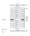
도1a는, 본 발명의 일 측면인 노광 장치(100)의 구성을 도시한 도면이다. 도1b는, 노광 장치(100)의 개략 단면도다. 노광 장치(100)는, 반도체장치등의 제조 공정에 사용되고, 기판 위에 패턴을 형성하는 리소그래피 장치다. 노광 장치(100)는, 본 실시 형태에서는, 원판(25)과 기판(27)을 주사 방향으로 이동시키면서 기판(27)을 노광(주사 노광)하여서, 원판(25)의 패턴을 기판(27) 위에 전사하는 스텝 앤드 스캔 방식의 노광 장치(스캐너)이다. 단, 노광 장치(100)는, 스텝 앤드 리피트 방식이나 그 밖의 노광 방식을 채용하는 것도 가능하다.
1A is a diagram showing the configuration of an
노광 장치(100)는, 도1a 및 1b에 도시된 바와 같이, 광원(1)으로부터의 광으로 원판(25)(레티클 또는 마스크)을 조명하는 조명 광학계(110)와, 원판(25)의 패턴을 기판(27)(웨이퍼나 유리 플레이트등)에 투영하는 투영 광학계(26)를 구비한다. 노광 장치(100)는, 원판 스테이지(29)와, 기판 스테이지(28)와, 제어부(50)를 구비한다. 기판 스테이지(28)는, 기판면내에서 서로 직교하는 제1방향 및 제2방향으로 이동하는 기능을 가진다. 본 실시 형태에서는, 기판 스테이지(28)를 기준으로서, 도1a 및 1b에 도시한 바와 같이, 제1방향을 y방향(y축), 제2방향을 x방향(X축), 제1방향 및 제2방향에 직교하는 방향을 z방향(z축)이라고 하는 좌표계를 정의한다. z방향은, 투영 광학계(26)의 광축방향에 상당하는 방향이다.
As shown in FIGS. 1A and 1B, the
광원(1)은, 파장 약 365nm의 수은 램프나, 파장 약 248nm의 KrF엑시머 레이저, 파장 약 193nm의 ArF엑시머 레이저등의 엑시머 레이저등을 구비한다. 광원(1)은, 원판(25)을 조명하기 위한 광(노광 광)을 사출한다.
The
조명 광학계(110)는, 릴레이 광학계(2)와, 사출각도 보존 광학소자(5)와, 회절광학 소자(6)와, 콘덴서 렌즈(7)와, 차광 부재(8)와, 프리즘 유닛(10)과, 줌렌즈 유닛(11)을 구비한다. 조명 광학계(110)는, 옵티컬 인티그레이터(12)와, 조리개(13)와, 콘덴서 렌즈 15와, 차광 유닛(19)과, 마스킹 유닛(20)과, 콘덴서 렌즈 21과, 콜리메이터 렌즈(23)를 더 구비한다.
The illumination
릴레이 광학계(2)는, 광원(1)과 사출각도 보존 광학소자(5)와의 사이에 설치되어 있다. 릴레이 광학계(2)는, 광원(1)으로부터의 광을 사출각도 보존 광학소자(5)에 이끈다. 사출각도 보존 광학소자(5)는, 회절광학 소자(6)의 광원측에 설치되어 있다. 사출각도 보존 광학소자(5)는, 플라이 아이 렌즈, 마이크로렌즈 어레이, 파이버 다발 등의 옵티컬 인티그레이터를 구비한다. 사출각도 보존 광학소자(5)는, 광원(1)으로부터의 광을, 그 발산 각도를 일정하게 유지하면서 회절광학 소자(6)에 이끈다. 사출각도 보존 광학소자(5)는, 광원(1)의 출력 변동이 회절광학 소자(6)에 의해 형성되는 광강도 분포(패턴 분포)에 끼치는 영향을 저감한다.
The relay
회절광학 소자(6)는, 조명 광학계(110)의 동공면(14)과 푸리에 변환의 관계에 있는 면에 배치되어 있다. 회절광학 소자(6)는, 투영 광학계(26)의 동공면과 공역한 면인 조명 광학계(110)의 동공면(14)이나, 조명 광학계(110)의 동공면(14)과 공역한 면에, 광원(1)으로부터의 광의 광강도 분포를 회절 작용에 의해 변환해서 원하는 광강도 분포를 형성한다. 회절광학 소자(6)는, 회절 패턴면에 원하는 회절 패턴이 얻어지도록 계산기로 설계된 계산기 홀로그램(CGH:Computer Generated Hologram)으로 구성되어 있어도 좋다. 본 실시 형태에서는, 투영 광학계(26)의 동공면에 형성되는 광원형상을 유효광원형상이라고 칭한다. 「유효광원」이란, 피조명면 및 피조명면의 공역면에 있어서의 광강도 분포 또는 광각도 분포를 의미한다. 회절광학 소자(6)는, 사출각도 보존 광학소자(5)와 콘덴서 렌즈(7)와의 사이에 설치되어 있다.
The diffraction optical element 6 is arranged on a plane in a Fourier transform relationship with the
조명 광학계(110)에는, 복수의 회절광학 소자(6)가 설치되어도 좋다. 예를 들면, 복수의 회절광학 소자(6)의 각각은 터릿(미도시됨)의 복수의 슬롯 중 하나에 부착되어 있다. 이 복수의 회절광학 소자(6)는, 각각, 상이한 유효광원형상을 형성한다. 이것들의 유효광원형상은, 소원형 형상(비교적 작은 원형형상), 대원형 형상(비교적 큰 원형형상), 윤대(annular) 형상, 2중극 형상, 4중극 형상, 그 밖의 형상을 구비한다. 윤대 형상, 2중극 형상 또는 4중극 형상의 유효광원형상으로 피조명면을 조명하는 방법은, 변형 조명이라고 불린다.
A plurality of diffractive optical elements 6 may be provided in the illumination
사출각도 보존 광학소자(5)로부터의 광은, 회절광학 소자(6)에 의해 회절되어, 콘덴서 렌즈(7)에 인도된다. 콘덴서 렌즈(7)는, 회절광학 소자(6)와 프리즘 유닛(10)과의 사이에 설치되고, 회절광학 소자(6)에 의해 회절된 광을 집광하고, 푸리에 변환면(9)에 분포 패턴(광강도 분포)을 형성한다.
Light from the exit angle preserving optical element 5 is diffracted by the diffraction optical element 6 and guided to the condenser lens 7. The condenser lens 7 is provided between the diffraction optical element 6 and the
푸리에 변환면(9)은, 옵티컬 인티그레이터(12)와 회절광학 소자(6)와의 사이에 있고, 회절광학 소자(6)와 광학적으로 푸리에 변환의 관계에 있는 면이다. 조명 광학계(110)의 광로에 배치되는 회절광학 소자(6)를 교환함으로써, 푸리에 변환면(9)에 형성되는 상기 분포 패턴의 형상을 변경할 수 있다.
The
차광 부재(8)는, 조명 광학계(110)의 광축(1b)과 수직한 방향으로 이동가능하게 구성되고, 푸리에 변환면(9)의 상류측(광원측)에 배치되어 있다. 차광 부재(8)는, 푸리에 변환면(9)의 위치로부터 약간 이격된(디포커스된) 위치에 배치되어 있다.
The
프리즘 유닛(10) 및 줌렌즈 유닛(11)은, 푸리에 변환면(9)과 옵티컬 인티그레이터(12)와의 사이에 설치되어 있다. 프리즘 유닛(10) 및 줌렌즈 유닛(11)은, 푸리에 변환면(9)에 형성된 광강도 분포를 확대하는 줌 광학계로서 기능한다. 프리즘 유닛(10)은, 푸리에 변환면(9)에 형성된 광강도 분포를, 윤대율 등을 조정하여 줌렌즈 유닛(11)에 이끈다. 줌렌즈 유닛(11)은, 프리즘 유닛(10)과 옵티컬 인티그레이터(12)와의 사이에 설치되어 있다. 줌렌즈 유닛(11)은, 예를 들면, 복수의 줌렌즈를 구비한다. 줌렌즈 유닛(11)은, 푸리에 변환면(9)에 형성된 광강도 분포를, 조명 광학계(110)의 개구수(NA)와 투영 광학계(26)의 NA와의 비를 기준으로 하여 얻어진 σ값을 조정하여 옵티컬 인티그레이터(12)에 이끈다.
The
옵티컬 인티그레이터(12)는, 줌렌즈 유닛(11)과 콘덴서 렌즈(15)와의 사이에 설치되어 있다. 옵티컬 인티그레이터(12)는, 윤대율, 개구각 및 σ값이 조정된 광강도 분포에 따라, 다수의 2차 광원을 형성하여 콘덴서 렌즈(15)에 이끄는 플라이 아이 렌즈를 구비한다. 단, 옵티컬 인티그레이터(12)는, 플라이 아이 렌즈 대신에, 옵티컬 파이프, 회절광학 소자, 마이크로렌즈 어레이 등의 다른 광학소자를 구비하여도 좋다. 옵티컬 인티그레이터(12)는, 회절광학 소자(6)를 경과한 광으로 피조명면(24)에 배치된 원판(25)을 균일하게 조명한다. 옵티컬 인티그레이터(12)와 콘덴서 렌즈(15)와의 사이에 있어서, 조명 광학계(110)의 동공면(14)의 근방에는, 조리개(13)가 설치되어 있다.
The
콘덴서 렌즈(15)는, 옵티컬 인티그레이터(12)와 원판(25)과의 사이에 설치되어 있다. 이에 따라, 콘덴서 렌즈(15)는, 옵티컬 인티그레이터(12)로부터 이끌어진 다수의 광선을 집광하여 원판(25)을 중첩적으로 조명할 수 있다. 광선을 옵티컬 인티그레이터(12)에 입사하여 콘덴서 렌즈(15)에 의해 집광하면, 콘덴서 렌즈(15)의 초점면인 공역면(20a)은, 거의 직사각형 형상으로 조명된다.
The
콘덴서 렌즈(15)의 후방에는, 하프 미러(16)가 배치되어 있다. 하프 미러(16)에서 반사된 노광 광의 일부는, 광량측정 광학계(17)에 입사한다. 광량측정 광학계(17)의 후방에는, 광량을 측정하는 센서(18)가 배치되어 있다. 센서(18)로 측정된 광량에 따라, 노광 실행시의 광 노광이 적절히 제어된다.
Behind the
피조명면(24)과 공역한 면인 공역면(20a)에는, X블레이드와 Y블레이드를 구비하는 마스킹 유닛(20)이 배치되고, 거의 직사각형 광강도 분포로 조명된다. 마스킹 유닛(20)은, 원판(25)(피조명면 24)의 조명 범위를 획정하기 위해서 배치되고, 원판 스테이지(29) 및 기판 스테이지(28)에 동기하여 주사된다. 원판 스테이지(29)는, 원판(25)을 보유하면서 이동하는 스테이지다. 기판 스테이지(28)는, 기판(27)을 보유하면서 이동하는 스테이지다.
A masking
차광 유닛(19)은, 마스킹 유닛(20)(피조명면 24의 공역면 20a)으로부터 이격된(디포커스된) 위치에 설치되어 있다. 콘덴서 렌즈(21)로부터의 광속에 대하여 소정의 기울기를 가지는 미러(22)에서 반사된 광은, 콜리메이터 렌즈(23)를 통하여 원판(25)을 조명한다.
The
투영 광학계(26)는, 원판(25)의 패턴을 기판(27)에 투영한다. 도2는, 투영 광학계(26)의 단면을 모식적으로 도시한 도면이다. 투영 광학계(26)는, 도2에 도시한 바와 같이, 복수의 광학부재(렌즈나 미러등의 광학소자)를 구비한다. 투영 광학계(26)의 동공면(26a) 또는 그 동공면(26a) 근방에는, 개구지름을 가변으로 하는 개구조리개(261)가 설치되어 있다. 개구조리개(261)의 개구지름을 조정함으로써, 투영 광학계(26)의 NA를 원하는 값으로 설정할 수 있다. 원판(25)의 패턴 상의 해상성은, 투영 광학계(26)의 NA 및 유효광원형상에 의존하고 있다. 따라서, 투영 광학계(26)의 NA 및 유효광원형상을 적절하게 설정(선택)함으로써, 원판(25)의 패턴의 해상성을 향상시킬 수 있다.
The projection
투영 광학계(26)를 구성하는 광학부재의 재질에 관해서는, 광원으로부터 사출되는 노광 광의 파장에 따라서 사용가능한 재료가 한정된다. 광원으로서, 파장 약 365nm의 수은 램프를 사용하는 경우에는, 10종류정도의 재료로 만들어진 광학부재를 조합하는 것으로, 축상 색수차나 배율 색수차등을 양호하게 보정할 수 있다. 한편, 광원으로서, 파장 약 248nm의 KrF엑시머 레이저나 파장 약 193nm의 ArF엑시머 레이저 등의 엑시머 레이저를 사용할 경우에는, 이것들의 엑시머 레이저로부터의 노광 광을 투과하는 재료가 한정된다. 상기 엑시머 레이저의 투과성이나 가격을 고려하여, 현재의 상태에서는 석영만으로 투영 광학계를 구성하는 것이 일반적이다. 이 경우, 투영 광학계의 광학설계에 의해 색수차를 양호하게 보정하는 것은 곤란하기 때문에, 레이저의 파장 스펙트럼을 협대역화함으로써 투영 광학계의 색수차의 영향을 감소시키고 있다.
Regarding the material of the optical member constituting the projection
도1a 및 1b의 설명으로 되돌아간다. 제어부(50)는, CPU나 메모리등을 구비하는 컴퓨터(정보처리 장치)로 구성된다. 제어부(50)는, 상기 메모리에 기억된 프로그램에 따라, 노광 장치(100)의 각 부를 총괄적으로 제어함으로써 노광 장치(100)를 동작시킨다. 제어부(50)는, 기판(27)을 노광하는 노광 공정과 그 노광 공정에 관련된 각종의 공정을 제어한다. 예를 들면, 제어부(50)는, 본 실시 형태에서는, 원판(25)의 패턴을 조명하는 조명 형상(조명 광속)을 결정하는 공정을 행한다.
Returning to the description of Figs. 1A and 1B. The
최근, 3차원 메모리나 촬상 소자의 제조 공정에 있어서, 수μm 내지 수십μm의 두께의 관통 패턴을 형성하는 것이 요청되어 있다. 이러한 두꺼운 관통 패턴을 노광 장치에 의해 형성하기 위해서는, 투영 광학계의 초점심도를 확장하는 것이 요청된다. 실질적으로 초점심도를 확장하는 기술로서, 투영 광학계의 광축방향으로 초점위치를 어긋나게 하면서 다중 노광을 행하는 방법이 알려져 있다. 다중 노광의 일례로서, Focus Latitude Enhancement Exposure(FLEX)법이 알려져 있다. FLEX법에서는, 기판상의 영역의 각 점이 2이상의 디포커스 상태로 노광되도록, 예를 들면, 투영 광학계의 광축에 대하여 기판을 기울이면서 주사 노광이 행해진다. 다중 노광의 다른 예로서, Resolution Enhancement by Laser-spectrum Adjusted Exposure(RELAX)법이 알려져 있다. RELAX법에서는, 복수의 파장에서 광량 피크를 가지도록 레이저 광원의 파장 스펙트럼을 조정한다. In recent years, in the manufacturing process of a three-dimensional memory or imaging device, it has been requested to form a through pattern having a thickness of several μm to several tens of μm. In order to form such a thick through pattern with an exposure apparatus, it is required to expand the depth of focus of the projection optical system. As a technique for substantially extending the depth of focus, a method of performing multiple exposures while shifting the focal position in the optical axis direction of the projection optical system is known. As an example of the multiple exposure, the FPEC method is known. In the FLEX method, scanning exposure is performed while tilting the substrate with respect to the optical axis of the projection optical system, for example, so that each point of a region on the substrate is exposed in two or more defocused states. As another example of multi-exposure, o u o o n a l l l l l e u ju ju ju ju ju ju (r l u u u) is known. In the REIAX method, the wavelength spectrum of a laser light source is adjusted so as to have light quantity peaks at a plurality of wavelengths.
상이한 파장의 광선은, 투영 광학계에 잔존하는 축상 색수차나 코마 색수차 등의 광학특성의 영향을 받아, 투영 광학계의 광축방향의 상이한 위치에 각각 결상한다. 레이저 광원의 파장 스펙트럼을 조정함으로써, 광축방향의 결상위치를 변화시킬 수 있고, 그 결과로 초점심도를 확장하는 효과가 얻어진다. Light rays of different wavelengths form images at different positions in the optical axis direction of the projection optical system, respectively, under the influence of optical properties such as axial chromatic aberration and coma chromatic aberration remaining in the projection optical system. By adjusting the wavelength spectrum of the laser light source, the imaging position in the optical axis direction can be changed, and as a result, the effect of extending the depth of focus is obtained.
이렇게, RELAX법에서는, 투영 광학계에 잔존하는 축상 색수차를 활용함으로써 초점심도를 확장하는 효과를 얻고 있지만, 투영 광학계에는 축상 색수차이외에도 배율 색수차나 코마 수차등의 수차가 잔존하고 있고, 이것들의 수차에 의해 결상성능의 저하를 초래할 수도 있다. In this way, in the REIAX method, the effect of extending the depth of focus is obtained by utilizing the axial chromatic aberration remaining in the projection optical system. It may cause deterioration of imaging performance.
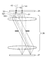
도3은, 투영 광학계의 배율 색수차가 결상성능에 주는 영향을 도시하는 모식도다. 도3은 원판(25)을 투과한 조명 광속이 투영 광학계(26)를 통과해서 기판(27)에 도달하는 상태를 도시하고 있다. 도3에는, 원판(25)의 축상물점으로부터의 광속 31과, 원판(25)의 축외물점으로부터의 광속 32가, 그려져 있다. 축상물점으로부터의 광속 31은, 축상 상점에 집광하는 광속 33이 되고, 축외물점으로부터의 광속 32는, 축외 상점에 집광하는 광속 35가 된다.
Fig. 3 is a schematic diagram showing the effect of the chromatic aberration of magnification of the projection optical system on the imaging performance. Fig. 3 shows a state in which the illumination light beam transmitted through the
여기에서, 원판(25)으로부터의 광속의 파장 스펙트럼에 복수의 피크가 포함되어 있을 경우, 같은 물점으로부터 출사한 광속이여도, 파장에 따라서 결상위치가 다르다. 여기에서는, 파장 스펙트럼에 있어서, 제1파장 및 제1파장과는 다른 제2파장에 피크를 가지는 것이라고 한다.
Here, when a plurality of peaks are included in the wavelength spectrum of the light flux from the
축상물점으로부터의 광속 31에 관해서, 제1파장의 광속(제1조명 광)은, 투영 광학계(26)를 통과하여 광속 33이 되어서 집광하고, 제2파장의 광속(제2조명 광)은, 투영 광학계(26)의 축상 색수차의 영향으로 광속 34가 되어서 집광한다. 광속 33의 광축방향의 결상위치와 광속 34의 광축방향의 결상위치와는 서로 다르다. 축상 광속에 관해서는, 배율 색수차의 영향은 거의 없기 때문에, 양쪽의 결상위치는 광축방향으로만 다르다.
Regarding the
한편, 축외물점으로부터의 광속 32에 관해서, 제1파장의 광속은, 투영 광학계(26)를 통과하여 광속 35가 되어서 집광하고, 제2파장의 광속은, 투영 광학계(26)의 축상 색수차 및 배율 색수차의 영향으로 광속 36이 되어서 집광한다. 광속 35와 광속 36의 결상위치는, 투영 광학계(26)의 광축방향뿐만 아니라, 광축방향과 수직한 방향에 대하여도 서로 다르다. 즉, 광속 35(제1조명 광)에 의해 결상되는 패턴 상과, 광속 36(제2조명 광)에 의해 결상되는 패턴 상과의 사이에는, 투영 광학계(26)의 광축방향과 그 광축방향에 수직한 방향과의 쌍방에 있어서 위치 편차가 생긴다.
On the other hand, for the
이상과 같이, 축외 광속에 관해서, 제1조명 광의 집광 위치와 제2조명 광의 집광 위치를 이은 직선은, 기판(27)에 대하여 수직하지 않는다. 그 때문에, 레지스트에 대하여 패턴 상이 비스듬히 형성되어, 그 결과로, 기판(27)위의 관통 패턴에 기울기가 생길 수 있다. 이 패턴 상의 기울기는, 주로 배율 색수차T와 축상 색수차L의 비율 T/L에 비례하여 생긴다.
As described above, with respect to the off-axis luminous flux, a straight line connecting the condensing position of the first illumination light and the condensing position of the second illumination light is not perpendicular to the
배율 색수차에 기인한 패턴 상의 위치 편차가 상점과 광축 사이의 거리에 비례하므로, 패턴 상의 기울기는 광축으로부터 상점의 거리로 증가한다. Since the positional deviation on the pattern due to chromatic aberration of magnification is proportional to the distance between the spot and the optical axis, the tilt on the pattern increases with the distance of the spot from the optical axis.
배율 색수차에 기인한 패턴의 기울기는, 배율 색수차에 의해 상이 어긋나는 방향으로 생긴다. 환언하면, 패턴의 기울기는, 투영 광학계(26)의 광축과 상면의 교점에 대하여, 방사 방향으로 생긴다. 스텝 앤드 스캔 방식의 노광 장치(스캐너)에서는, 슬릿형의 노광 영역을 주사함으로써 노광을 행한다. 즉, 투영 광학계(26)의 상면에 있어서 노광에 사용되는 영역은, 가늘고 긴 슬릿형이 된다. 그 때문에, 배율 색수차의 영향이 어떻게 나오는지, 다시 말해, 패턴의 기울기가 어떻게 나오는지는, 패턴의 방향에 따라 달라진다. 구체적으로는, 슬릿형의 노광 영역에 대하여 횡방향으로 연장된 패턴에는 기울기가 발생하고, 길이 방향으로 연장된 패턴에는 기울기가 발생하지 않는다. 패턴의 상기 방향에 따라 생기는 기울기가 다른 점에는 주의가 필요하다. 패턴의 기울기가 허용 값이상이 되면, 디바이스 불량의 원인이 되고, 수율이 저하할 수 있다.
The inclination of the pattern due to the chromatic aberration of magnification occurs in the direction in which the image is shifted due to the chromatic aberration of magnification. In other words, the inclination of the pattern occurs in the radial direction with respect to the intersection of the optical axis of the projection
본 실시 형태에서는, 제1파장의 광속의 집광 위치와 제2파장의 광속의 집광 위치 사이의 위치 편차에 기인한 패턴 상의 기울기를 보정하기 위해서, 조명 광속의 기울기를 조정한다. 이후, 조명 광속의 기울기를 조정하는 동작을 텔레센트리시티 조정이라고 한다. 도4는, 원판(25)으로부터의 광속이 투영 광학계(26)를 통과하여 기판(27)에 도달하는 상태를 도시하고 있다. 도4에 있어서, 광선 41, 42, 43은, 각각 원판(25)을 조명하는 조명 광속의 주 광선을 나타낸다. 주 광선 41은, 축상물점을 조명한다. 주 광선 42 및 43은, 축외물점을 조명한다. 주 광선 43은, 투영 광학계(26)의 내부를 광선 322로 나타낸 바와 같이 나아가고, 기판(27)에 대하여 대략 수직한 광선이 되어서, 상점에 도달한다. 주 광선 42는, 투영 광학계(26)의 내부를 광선 321로 나타낸 바와 같이 나아가고, 기판(27)에 대하여 수직한 방향으로부터 기운 광선이 되어서, 그 상점에 도달한다. 이렇게, 원판(25)에 입사하는 주 광선의 기울기를 변화시키는 것으로, 기판(27)에 집광되는 광속의 기울기를 조정할 수 있고, 그 결과로 패턴 상을 기울게 하는 효과가 얻어진다. 즉, RELAX법에 의한 패턴 상의 기울기량과, 텔레센트리시티 조정에 의한 패턴 상의 기울기량을 적절히 제어함에 의해, 패턴의 기울기를 감소시키는 것이 가능하다.
In the present embodiment, the inclination of the illumination light flux is adjusted in order to correct the inclination on the pattern due to the positional deviation between the convergence position of the light flux of the first wavelength and the convergence position of the light flux of the second wavelength. Hereafter, an operation of adjusting the inclination of the illumination light flux is referred to as telecentricity adjustment. Fig. 4 shows a state in which the light flux from the
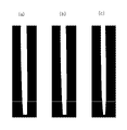
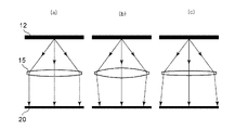
도5a 내지 5c는, 텔레센트리시티 조정에 의해 패턴의 기울기가 감소되는 것을 도시한 도면이다. 도5a 내지 5c는, 축외 광속에 의해 형성되는 패턴 상의 형상을 각각 도시하고 있다. 이 패턴 상들은 시뮬레이션에 의해 얻어진다. 조명 조건은, NA=0.55, σ=0.50, 패턴은 구경 200nm의 트렌치, 레지스트의 두께는 4μm로서 시뮬레이션을 행한 결과다. 여기에서, σ는, 조명 광학계(110)의 개구수(NA)와 투영 광학계(26)의 NA와의 비율을 기준으로 한 값이다.
5A to 5C are diagrams showing that the slope of a pattern is reduced by telecentricity adjustment. 5A to 5C each show a shape on a pattern formed by an off-axis light flux. These pattern images are obtained by simulation. Illumination conditions are results of simulations as follows: NA = 0.55, σ = 0.50, the pattern is a trench with an aperture of 200 nm, and the resist thickness is 4 μm. Here, σ is a value based on the ratio of the NA of the illumination
도5a는, 텔레센트리시티 조정을 행하지 않은 경우의 결과를 도시하고 있다. 도5b는, 텔레센트리시티를 0.05만큼 조정했을 경우의 결과를 도시하고 있다. 도5c는, 텔레센트리시티를 0.10만큼 조정했을 경우의 결과를 도시하고 있다. Fig. 5A shows the result when telecentricity adjustment is not performed. Fig. 5B shows the result when the telecentricity is adjusted by 0.05. Fig. 5C shows the result when the telecentricity is adjusted by 0.10.
여기에서, 텔레센트리시티를 0.05만큼 조정한다고 하는 의미는, 투영 광학계(26)의 광축방향으로부터의 기울기 각이 θ인 경우, θ=arctan 0.05만큼 조명 광속의 기울기를 조정한다고 하는 의미다. 도5a 내지 5c에 도시된 바와 같이, 조명 광속의 기울기를 증가시킴에 따라 상기 패턴의 기울기가 감소되는 것처럼 보인다.
Here, adjusting the telecentricity by 0.05 means adjusting the inclination of the illumination beam by 0.05 when the inclination angle of the projection
도6은, 조명 광속의 기울기와 패턴 상의 기울기와의 관계를 도시한 그래프다. 패턴 상의 기울기는, 패턴 상의 좌우의 벽의 중점 위의 선형 회귀를 행하여서 얻어진 직선의 기울기로서 표기하고 있다. 조명 광속의 기울기가 증가함에 따라서, 상기 직선의 기울기가 감소되어서, 패턴 상의 기울기를 감소시킨다. 여기에서는, 시뮬레이션에 의해, 조명 광속의 기울기와 패턴 상의 기울기와의 관계를 구한다. 또는, 실제의 패턴 형성의 결과에 따라 이러한 관계를 구해도 좋다. Fig. 6 is a graph showing the relationship between the slope of the illumination light flux and the slope of the pattern. The gradient on the pattern is expressed as the gradient of a straight line obtained by performing linear regression on the midpoint of the left and right walls on the pattern. As the inclination of the illumination beam increases, the inclination of the straight line decreases, thereby reducing the inclination on the pattern. Here, the relationship between the inclination of the illumination light flux and the inclination of the pattern is obtained by simulation. Alternatively, you may obtain such a relationship according to the result of actual pattern formation.
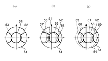
조명 광속의 기울기와 패턴 상의 기울기와의 관계는, 패턴 형상에 따라 변화된다. 이것은, 도7a 내지 7c를 참조하여 설명한다. 도7a 내지 7c는, 원판(25)에 있어서의 축외물점으로부터의 광속에 의해 형성되는 광강도 분포를 각기 도시하고, 투영 광학계(26)의 동공면에 있어서의 광강도 분포를 각기 도시하고 있다. 도7a는, 파장 스펙트럼에 1개의 피크를 가지는 광속을 사용해서 노광을 행했을 때의 광강도 분포를 도시하고 있다. 참조 부호 54는, 투영 광학계(26)의 개구조리개에 의해 결정되는 동공을 나타낸다. 참조 부호 51은, 축외물점으로부터의 0차 회절광속을 나타낸다. 참조 부호 52, 53은 각각, 조명 광속이 원판(25)의 패턴으로 회절된 양 및 음의 1차 회절광속을 나타낸다.
The relationship between the inclination of the illumination light flux and the inclination on the pattern changes depending on the pattern shape. This is explained with reference to Figs. 7A to 7C. 7A to 7C respectively show the light intensity distribution formed by the light flux from the off-axis object point on the
도7a에 있어서는, 0차 회절광속의 광강도 분포는 동공 중심으로 위치하고 있고, 양 및 음의 1차 회절광속의 동공 주변영역에 있어서의 이클립스(eclipse)도 좌우 대칭이기 때문에, 투영 광학계(26)에 디포커스가 생길 때에도 상면에는 패턴 상의 위치 편차가 대부분 생기지 않는다. 즉, 패턴 상은 대부분 기울지 않는다.
In Fig. 7A, the light intensity distribution of the 0th-order diffraction light flux is located at the center of the pupil, and the eclipse in the pupil peripheral area of the positive and negative 1st-order diffraction light fluxes is also symmetrical, so the projection
도7b는, 도7a의 상태로부터 조명 광속의 기울기를 조정했을 때의 광강도 분포를 도시하고 있다. 주 광선을 비스듬히 입사시키므로, 동공면에 있어서의 0차 회절광속의 광강도 분포(55)는 동공중심으로부터 어긋나 있다. 양 및 음의 1차 회절광속 56, 57의 동공 주변영역에 있어서의 이클립스가 좌우 비대칭이기 때문에, 동공면에 있어서의 광강도 분포의 대칭성이 저하하고 있다. 그 때문에, 투영 광학계(26)에 디포커스가 생겼을 때, 상면에 있어서 패턴 상의 위치 편차가 생기고, 패턴 상이 기운다.
FIG. 7B shows the light intensity distribution when the inclination of the illumination light flux is adjusted from the state of FIG. 7A. Since the chief ray is obliquely incident, the
원판(25)의 패턴의 형상(예를 들면, 라인 앤드 스페이스 패턴에 있어서의 패턴 피치, 라인과 스페이스와의 비, 패턴의 배열 방향 등)에 따라서 회절광속의 발생의 방법이 변화되고, 동공 주변영역에 있어서의 이클립스도 변화된다. 이에 따라, 동공면에 있어서의 광강도 분포의 비대칭성도 변화되어서, 광량중심도 마찬가지로 변화된다. 이것은, 투영 광학계(26)에 디포커스가 생기는 경우의 상면에 있어서의 패턴 상의 위치 편차량에 차이가 생기는 것을 의미한다. 따라서, 원판(25)의 패턴 형상에 따라 패턴의 기울기의 조정의 쉬움이 달라지는 것처럼 보인다.
Depending on the shape of the pattern of the original plate 25 (for example, the pattern pitch in the line-and-space pattern, the ratio of lines and spaces, the arrangement direction of the pattern, etc.), the method of generating the diffracted light flux changes, and the pupil periphery The eclipse in the area also changes. As a result, the asymmetry of the light intensity distribution on the pupil plane also changes, and the light quantity center also changes in the same way. This means that a difference arises in the amount of positional deviation on the pattern on the image plane when defocusing occurs in the projection
그 다음에, 조명 광속의 텔레센트리시티 조정의 방법에 대해서, 도8a 내지 8c를 참조하여 설명한다. 도8a 내지 8c는, 조명 광학계(110)의 일부를 각각 도시한 간단한 도면이다. 도8a 내지 8c에서는, 옵티컬 인티그레이터(12)로부터, 원판(25)과 공역한 면인 공역면(20a)까지의 광로가 추출되어 도시되어 있다. 옵티컬 인티그레이터(12)의 출사면과 공역면(20a)은, 콘덴서 렌즈(15)를 통해 상과 동공의 관계(Fourier변환의 관계)로 되어 있다.
Next, a method of adjusting the telecentricity of the illumination light flux will be described with reference to Figs. 8A to 8C. 8A to 8C are simple diagrams showing a part of the illumination
도8a는, 옵티컬 인티그레이터(12)의 1점으로부터 출사한 광이, 공역면(20a)에 대략 수직으로 입사하는 기준 상태를 도시하고 있다. 도8a 내지 8c에서는, 콘덴서 렌즈(15)를 1매의 렌즈로서 그리고 있지만, 실제로는 복수의 렌즈로 구성되어 있다. 콘덴서 렌즈(15)를 구성하는 그 렌즈들의 일부를 줌 배율을 위해 이동시킴으로써, 콘덴서 렌즈(15) 전체의 초점거리를 변화시킬 수 있다. 콘덴서 렌즈(15)의 초점거리를 기준상태보다도 짧게 했을 경우에는, 도8b에 도시한 바와 같이, 축외의 광속은 광축에 가까이 가도록 공역면(20a)에 입사한다. 한편, 콘덴서 렌즈(15)의 초점거리를 기준상태보다도 길게 했을 경우에는, 도8c에 도시한 바와 같이, 축외의 광속은 광축으로부터 멀어지도록 공역면(20a)에 입사한다.
8A shows a reference state in which light emitted from one point of the
공역면(20a)은 피조명면(24)(원판 25)과 공역한 면이기 때문에, 이 면에 있어서의 광강도 분포는, 피조명면(24)(원판 25)에 있어서의 광강도 분포와 동일하다.
Since the
이상 설명한 바와 같이, 조명 광학계(110)에 구비된 상기 렌즈들의 줌 배율 상태를 변화시킴으로써, 피조명면(24)(원판 25)에 있어서의 광강도 분포를 조정할 수 있다. 즉, 원판(25)에 조사되는 주 광선의 기울기도 조정하는 것이 가능하다. 이렇게, 콘덴서 렌즈(15)의 초점거리를 줌 기구에 의해 연속적으로 변화시키는 것으로, 주 광선의 기울기량도 연속적으로 조정하는 것이 가능하다.
As described above, the light intensity distribution on the surface to be illuminated 24 (original plate 25) can be adjusted by changing the zoom magnification state of the lenses provided in the illumination
도8a 내지 8c에 도시한 바와 같이, 광축으로부터의 거리에 따라서 광선의 기울기의 변화가 증가하고, 투영 광학계(26)의 배율 색수차로 인해 생기는 패턴 상의 기울기도 광축으로부터의 거리에 따라서 증가한다. 그 때문에, 배율 색수차에 기인한 패턴 상의 기울기 조정에는, 도8a 내지 8c에 도시된 것처럼 줌 배율 상태를 변화시키는 방법이 적합하다.
As shown in Figs. 8A to 8C, the change in the inclination of the light beam increases with the distance from the optical axis, and the inclination of the pattern caused by the chromatic aberration of magnification of the projection
그 다음에, 투영 광학계(26)의 개구조리개(261)를 제어함으로써 패턴 상의 기울기를 조정하는 방법에 대해서, 도9를 참조하여 설명한다. 도9는, 원판(25)으로부터의 광속이 투영 광학계(26)를 통해서 기판(27)에 도달하는 상태를 도시하고 있다. 참조 번호 811은, 축상물점을 조명하는 광속(81)의 주 광선을 나타낸다. 참조 번호 82는 축외물점을 출사해서 축외상점에 도달하는 광속을 나타낸다.
Next, a method of adjusting the inclination on a pattern by controlling the
축상물점을 조명하는 광속 81의 주 광선 811과 축외물점을 조명하는 광속 82의 주 광선 821은, 원판(25)에 대하여 대략 수직으로 입사하고, 기판(27)에 대하여도 대략 수직으로 입사한다. 개구조리개(261)의 단부를 통과하는 주변 광선에 관해서는, 플러스측의 주변 광선 822와 마이너스측의 주변 광선 823이 기판(27)에 대하여 대략 동일한 입사각도로 입사한다. 그 때문에, 레지스트에 형성되는 패턴 상은 대부분 기울지 않는다.
The
여기에서, 도4에 도시한 바와 같이, 패턴의 기울기를 보정하기 위해서 텔레센트리시티가 조정되면, 축외물점을 조명하는 광속(82)의 주 광선 831은, 광축에 대하여 비스듬한 방향으로 상기 원판(25)에 입사하고, 광축에 대하여 비스듬한 방향으로 기판(27)에도 입사한다. 개구조리개(261)의 위치를 A로부터 B에 이동시키고, 추가로 개구조리개(261)의 개구지름을 변화시킴으로써, 주변 광선의 광로가 결정된다. 도9에 도시한 바와 같이, 플러스측의 주변 광선 832와 마이너스측의 주변 광선 833은 서로 다른 각도로 기판(27)에 입사하게 된다. 개구조리개(261)의 위치 및 개구지름을 적절히 설정함으로써, 주 광선 831과 플러스측의 주변 광선 832 사이에 형성된 각도와, 주 광선 831과 마이너스측의 주변 광선 833 사이에 형성된 각도를 대략 동일하게 할 수 있다. 이렇게 주변 광선의 광로를 적절히 설정함으로써, 패턴 상의 균일성을 유지하면서, 패턴 상의 기울기를 제어하는 것이 가능하다.
Here, as shown in FIG. 4, when the telecentricity is adjusted to correct the inclination of the pattern, the
투영 광학계(26)의 개구조리개(261)의 위치 및 개구지름을 제어했을 때의 투영 광학계(26)의 동공면에 있어서의 광강도 분포는, 도7c를 참조하여 설명한다. 도7b의 경우와 같이, 주 광선을 비스듬히 입사시키므로, 동공면에 있어서의 0차 회절광속의 광강도 분포(58)는 동공중심으로부터 어긋나 있다. 개구조리개(261)의 위치를 변화시키므로, 동공영역이 영역 54로부터 영역 61에 시프트 하고 있다. 이 결과, 양 및 음의 1차 회절광속 59, 60의 동공 주변영역에 있어서의 이클립스는, 0차 회절광속의 광강도 분포의 중심에 대하여 좌우 대칭이 된다. 도7a와 도7c를 서로 비교하면, 동공면에 있어서의 광강도의 전체가 시프트 하고 있고, 레지스트에 형성되는 패턴이 투영 광학계(26)의 광축방향과 수직한 방향으로 시프트 하게 된다.
The light intensity distribution on the pupil plane of the projection
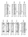
도10a 내지 10d는, 텔레센트리시티 조정과 개구조리개(261) 조정을 행하는 것에 의해 패턴 상의 기울기가 감소되는 것을 도시한 도면이다. 도10a 내지 10d는, 축외 광속에 의해 형성되는 패턴 상의 형상을 각기 도시하고 있다. 이 패턴 상들은 시뮬레이션에 의해 얻어진다. 조명 조건은, NA=0.55, σ=0.50, 패턴은 구경 200nm의 트렌치, 레지스트의 두께는 4μm로서 시뮬레이션을 행한 결과다. 도10a는, 텔레센트리시티 조정 및 개구조리개(261) 조정을 행하지 않은 경우의 결과를 도시하고 있다. 도10b는, 텔레센트리시티를 0.05만큼 조정하고, 개구조리개(261)를 그것에 따라서 조정했을 경우의 결과를 도시하고 있다. 도10c는, 텔레센트리시티를 0.10만큼 조정하고, 개구조리개(261)를 그것에 따라서 조정했을 경우의 결과를 도시하고 있다. 도10d는, 텔레센트리시티를 0.15만큼 조정하고, 개구조리개(261)를 그것에 따라서 조정했을 경우의 결과를 도시하고 있다.
10A to 10D are diagrams showing that the inclination on the pattern is reduced by performing the telecentricity adjustment and the
조명 광속의 기울기를 증가시킴에 따라 패턴의 기울기가 감소하는 것처럼 보인다. As the slope of the illumination beam increases, the slope of the pattern appears to decrease.
도11은, 조명 광속의 기울기와 패턴 상의 기울기와의 관계를 도시한 그래프다. 패턴 상의 기울기는, 패턴 상의 좌우의 벽의 중점 위의 선형 회귀를 행하여서 얻어진 직선의 기울기로서 표기하고 있다. 조명 광속의 기울기가 증가함에 따라서, 상기 직선의 기울기가 감소하여서, 패턴 상의 기울기를 감소시킨다. 여기에서는, 시뮬레이션에 의해, 조명 광속의 기울기와 패턴 상의 기울기와의 관계를 구하고 있다. 또는, 실제의 패턴 형성의 결과에 따라서 이러한 관계를 구해도 좋다. Fig. 11 is a graph showing the relationship between the slope of the illumination light flux and the slope of the pattern. The gradient on the pattern is expressed as the gradient of a straight line obtained by performing linear regression on the midpoint of the left and right walls on the pattern. As the inclination of the illumination beam increases, the inclination of the straight line decreases, thereby reducing the inclination on the pattern. Here, the relationship between the inclination of the illumination light flux and the inclination of the pattern is obtained by simulation. Alternatively, you may obtain such a relationship according to the result of actual pattern formation.
이상 설명한 바와 같이, 본 실시 형태의 노광 장치로는, 패턴을 조명하는 조명 광속의 기울기를 적절히 설정함으로써, 레지스트 막에 형성되는 패턴 상의 기울기를 효과적으로 저감시킬 수 있다. As described above, in the exposure apparatus of the present embodiment, the inclination of the pattern formed on the resist film can be effectively reduced by appropriately setting the inclination of the illumination beam for illuminating the pattern.
변형 예 variant example
도9에서는, 개구조리개(261)의 위치를 변화시키고 있다. 또는, 복수의 개구조리개를 준비하고, 위치A와 위치B의 쌍방에 개구지름이 가변하는 개구조리개를 배치해도 좋다. 원판(25)에 대하여 대략 수직으로 광속을 입사시킬 경우에는, 위치B에 배치된 개구조리개의 지름을 증가시켜 광선에 이클립스를 방지하도록 하고, 위치A에 배치된 개구조리개의 지름을 적절히 설정한다. 원판(25)에 대하여 비스듬히 광속을 입사시킬 경우에는, 위치A에 배치된 개구조리개의 지름을 증가시켜 광선에 이클립스를 방지하도록 하고, 위치B에 배치된 개구조리개의 지름을 적절히 설정한다.
In Fig. 9, the position of the
노광 장치에 있어서의 노광 모드 Exposure mode in exposure apparatus
메모리나 촬상 소자등의 반도체장치의 제조 공정에는, 기판 위에 패턴층을 형성하는 공정이 포함된다. 해당 공정에 있어서 노광 장치를 사용해서 레지스트에 패턴 상이 형성되고, 에칭 처리 등을 거쳐서 트렌치를 구비하는 패턴층이 형성된다. 형성하는 패턴층에 따라 사용된 레지스트의 두께가 다를 수 있고, 레지스트의 두께에 따라서 노광 장치의 투영 광학계에 사용된 초점심도도 다르다. 레지스트의 두께가 두꺼울 경우에는, RELAX법 등의 다중노광에 의해 패턴 형성이 행해질 수 있다. RELAX법에서는, 복수의 파장으로 광량 피크를 가지도록 레이저 광원의 발진 상태를 제어할 필요가 있다. 한편으로, 레지스트의 두께가 얇을 경우에는, 단일의 파장으로 광량 피크를 가지도록 레이저 광원의 발진 상태가 제어된다. BACKGROUND OF THE INVENTION A process of manufacturing a semiconductor device such as a memory or an imaging device includes a process of forming a pattern layer on a substrate. In this step, a pattern image is formed on the resist using an exposure device, and a pattern layer having a trench is formed through an etching process or the like. Depending on the pattern layer to be formed, the thickness of the resist used may be different, and the depth of focus used in the projection optical system of the exposure apparatus is also different according to the thickness of the resist. When the thickness of the resist is thick, pattern formation can be performed by multiple exposures such as the RELAX method. In the REIAX method, it is necessary to control the oscillation state of the laser light source so as to have a light quantity peak at a plurality of wavelengths. On the other hand, when the thickness of the resist is thin, the oscillation state of the laser light source is controlled so as to have a light quantity peak at a single wavelength.
이렇게, 기판 위에 형성하는 층마다 투영 광학계의 초점심도 등을 변화시킬 필요가 있기 때문에, 노광 장치에 있어서의 노광 모드를 적절히 전환 가능할 수 있다. 예를 들면, 노광 모드에 따라, 레이저 광원의 발진 상태를 전환하는 것이 생각될 수 있다. 레이저 광원의 발진 상태를 전환시키기 위해서, 광원에는 발진 상태를 전환가능한 기구가 설치되어 있다. 노광 장치는, 노광시의 각종 파라미터가 설정된 레시피에 따라서 레이저 광원의 발진 상태를 전환할 수 있다. In this way, since it is necessary to change the depth of focus of the projection optical system for each layer formed on the substrate, the exposure mode in the exposure apparatus can be appropriately switched. For example, it is conceivable to switch the oscillation state of the laser light source according to the exposure mode. In order to switch the oscillation state of the laser light source, the light source is provided with a mechanism capable of switching the oscillation state. The exposure apparatus can switch the oscillation state of the laser light source according to a recipe in which various parameters at the time of exposure are set.
예를 들면, 제1모드와 제2모드와의 사이에서 노광 모드를 전환 가능할 수 있다. 제1모드는, 단일의 파장(기준파장)으로 광량 피크를 가지도록 레이저 광원의 발진 상태를 제어해서 노광을 행하는 모드다. 제2모드는, 기준파장과는 다른 제1의 파장의 제1조명 광과, 그 기준파장 또는 제1의 파장과는 다른 제2의 파장의 제2조명 광을 포함하는, 조명 광으로 노광을 행하는 모드다. 제2모드에 있어서의 축외 광속의 원판에의 입사각과, 제1모드에 있어서의 축외 광속의 원판에의 입사각을 다르게 하는 것에 의해, 제2모드에 있어서, 패턴 상의 기울기의 발생을 감소시킬 수 있다. For example, the exposure mode may be switched between the first mode and the second mode. The first mode is a mode in which exposure is performed by controlling the oscillation state of the laser light source so as to have a light quantity peak at a single wavelength (reference wavelength). In the second mode, exposure is performed with illumination light including first illumination light having a first wavelength different from the reference wavelength and second illumination light having a second wavelength different from the reference wavelength or the first wavelength. mode to do By making the incident angle of the off-axis light flux on the original plate in the second mode different from the incident angle of the off-axis light flux on the original plate in the first mode, the occurrence of inclination on the pattern can be reduced in the second mode. .
제2모드로, RELAX법에 근거하는 노광을 행할 경우에는, 광량 피크에 대응하는 복수의 파장의 값이나 파장차이를 지정할 필요가 있기 때문에, 이 파라미터들을 레시피의 설정 항목의 1개라고 하면 좋다. RELAX법에 근거하는 노광을 위해 조명 광속의 기울기 조정과 개구조리개의 조정을 행하기 위해, 레시피에 의해 노광 장치가 자동으로 행하도록 구성되어도 좋고, 유저에게 조정을 행할 것인가 아닌가의 판단을 요구하여도 좋다. 노광 장치가 상기 조정을 자동으로 행할 경우에는, 패턴의 특징이나 조명 광속의 텔레센트리시티 등을 고려하여 조정량이 결정된다. 이때, 노광 장치는, 원판의 패턴의 특징에 관한 정보를 취득할 수 있도록 구성될 수 있다. In the second mode, when exposure based on the RELAX method is performed, since it is necessary to designate a plurality of wavelength values and wavelength differences corresponding to the light quantity peak, these parameters may be regarded as one of the setting items of the recipe. In order to adjust the inclination of the illumination beam and the adjustment of the aperture diaphragm for exposure based on the REAX method, the exposure apparatus may be configured to automatically perform the adjustment according to a recipe, or even if the user is requested to determine whether to perform the adjustment or not good night. When the exposure apparatus automatically performs the above adjustment, the adjustment amount is determined in consideration of the characteristics of the pattern, the telecentricity of the illumination light flux, and the like. At this time, the exposure apparatus may be configured to acquire information about the characteristics of the pattern of the original plate.
물품의 제조 방법 Method of manufacturing the article
본 실시 형태에 대표되는 노광 장치를 이용해서 반도체장치(메모리나 촬상 소자 등의 광전변환 장치)를 제조하는 방법에 대해서 설명한다. 본 실시 형태의 노광 장치는, 후막 공정을 포함하는 반도체장치의 제조 방법에 적합하게 사용된다. 촬상 소자(광원 변환장치)에 있어서의 화소분리부의 형성 공정은, 상기 후막 공정의 일례다. A method of manufacturing a semiconductor device (a photoelectric conversion device such as a memory or an imaging device) using the exposure apparatus represented by the present embodiment will be described. The exposure apparatus of the present embodiment is suitably used in a semiconductor device manufacturing method including a thick film step. The process of forming the pixel separator in the imaging element (light source converter) is an example of the thick film process.
이하, 도12를 참조하여 촬상 소자의 제조 공정에 있어서의 화소분리부의 형성 공정에 대해서 설명한다. 단계 S101에 있어서, 서로 반대측의 면인 제1면S1 및 제2면S2를 가지는 반도체 기판(101)을 준비한다. 반도체 기판(101)은, 전형적으로는, 실리콘 기판 혹은 실리콘층이다. 그 다음에, 단계 S102에 있어서, 반도체 기판(101)의 제1면S1 위에 절연막(예를 들면, 실리콘 산화막)(102)을 형성한다.
Hereinafter, with reference to FIG. 12, a process of forming a pixel separator in a manufacturing process of an imaging device will be described. In step S101, a
그 다음에, 단계 S103에 있어서, 반도체 기판(101)의 제1면S1 위, 보다 구체적으로는, 반도체 기판(101)의 제1면S1 위의 절연막(102) 위에, 레지스트(103)를 도포한다. 게다, 단계 S104에 있어서, 상술한 실시 형태에서 설명한 바와 같이, 조명 광속의 기울기를 조정한 상태로 노광 동작을 행하는 것에 의해, 레지스트(103)에 패턴 상을 형성하고, 에칭 처리 등을 통해 홈(트렌치)(104)을 형성한다. 레지스트(103)에 형성되는 패턴 상의 기울기를 감소시키는 것으로, 기울기가 감소된 홈(104)을 형성할 수 있다.
Then, in step S103, a resist 103 is applied on the first surface S1 of the
그 다음에, 단계 S105에 있어서, 반도체 기판(101)을 드라이 에칭법 등에 의해 에칭함에 의해, 반도체 기판(101)의 제1면S1 위에 홈(105)을 형성한다. 이 에칭에 있어서 반도체 기판(101)의 제1면S1을 보호하기 위해서, 레지스트(103)를 두껍게 도포하는 것이 요청된다.
Next, in step S105, the
그 다음에, 단계 S106에서는, 그 레지스트(103)를 제거한 후에, 홈(105)을 통해 반도체 기판(101)에 이온을 주입함으로써 게터링 영역(106)을 형성한다. 다시 말해, 단계 S106에서는, 반도체 기판(101)의 제1면S1 중 홈(105)이 존재하는 영역이외의 영역이 절연막(102)으로 마스크 된 상태에서 상기 홈(105)을 통해 반도체 기판(101)에 이온을 주입한다. 각 게터링 영역(106)은, 홈(105)의 바닥 아래에 위치된 제1부분과, 홈(105)의 측방에 위치된 제2부분을 구비할 수 있다. 일례에 있어서, 해당 제1부분에 있어서의 제14족원소의 농도가, 해당 제2부분에 있어서의 제14족원소의 농도보다도 높다. 이온은, 반도체 기판(101)이 실리콘 기판일 경우, 실리콘이외의 제14족원소의 이온일 수 있다. 이온의 주입에는, 이온 주입 장치가 사용된다. 이온을 주입하기 위한 가속 에너지는, 하드 마스크로서의 절연막(102)을 이온이 관통하고서 반도체 기판(101)에 도달하지 않도록 결정될 수 있다. 예를 들면, 이온 주입시에 절연막(102)의 두께가 300nm일 때, 가속 에너지가 20keV정도이면 이온이 절연막(102)을 대부분 관통하지 않는다.
Then, in step S106, after the resist 103 is removed, the
반도체 기판(101)이 실리콘 기판일 경우, 단계 S106에 있어서 반도체 기판(101)에 주입되는 이온을 구성하는 재료는, 탄소가 적합하다. 또는, 탄소를 포함하는 분자인 탄화수소가 채용되어도 좋다. 반도체 기판(101)이 실리콘 기판일 경우, 단계 S106에 있어서 반도체 기판(101)에 주입되는 이온을 구성하는 재료는, 게르마늄, 주석 또는 납이어도 좋다. 반도체 기판(101)으로서의 실리콘 기판에 탄소, 게르마늄, 주석 또는 납의 이온을 주입함으로써, 실리콘 기판에 국소적 변형을 주고, 그 실리콘 기판을 게터링 사이트로서 기능시킬 수 있다. 홈(105)을 통해 반도체 기판(101)에 이온을 주입함으로써, 비교적 낮은 가속 에너지로도, 반도체 기판(101)의 깊은 위치에 게터링 영역(106)을 형성할 수 있다.
When the
그 다음에, 단계 S107에 있어서, 절연막(102)이 제거된다. 단계 S108에 있어서, 홈(105)내에 절연체가 배치 혹은 충전되도록, 예를 들면, 감압CVD법 등의 막형성 방법에 의해, 홈(105)내 및 반도체 기판(101)의 제1면S1 위에, 절연막(예를 들면, 실리콘 질화막)(107)을 형성한다. 그 다음에, 단계 S109에 있어서, 절연막(107) 중, 반도체 기판(101)의 제1면S1 위에 존재하는 부분을 CMP법 등에 의해 제거한다. 이에 따라, 절연막(107) 중, 홈(105)내에 존재하는 부분이, 홈(105)에 배치 혹은 충전된 화소분리부(108)로서 남는다.
Then, in step S107, the insulating
단계 S108 및 단계 S109는, 반드시 실시되지 않는다. 단계 S108 및 단계 S109가 실시되지 않은 경우에는, 홈(105)이 공극으로서 남고, 이 공극이 화소분리부로서 기능할 수 있다. 각 홈(105)내에 배치되는 화소분리부(108)는 홈(105)을 완전히 충전할 필요는 없고, 홈(105)내에 공극이 존재되어도 좋다. 화소분리부(108)는 절연체만으로 만들어져도 좋지만, 절연체와 비절연체(반도체 혹은 도전체)를 조합한 구조이어도 좋다. 이 경우, 비절연체와 반도체 기판(101)과의 접촉을 피하기 위해서, 절연체가 비절연체와 반도체 기판(101)과의 사이에 배치될 수 있다.
Steps S108 and S109 are not necessarily performed. In the case where steps S108 and S109 are not carried out, the
이상 설명한 바와 같이, 반도체 기판(101)에 홈(105)을 형성하는 제1형성 단계와, 홈(105)내에 화소분리부(108)를 형성하는 제2형성 단계를 경과하여, 화소분리부(108)가 형성된다. 그 후, 복수의 화소분리부의 사이의 영역에 전하축적 영역, 게이트 전극등이 형성되고, 그 결과로 촬상 소자가 만들어진다.
As described above, after the first formation step of forming the
본 발명을 실시 형태들을 참조하여 기재하였지만, 본 발명은 상기 개시된 실시 형태들에 한정되지 않고 아래의 청구항의 범위에 의해 정의된다는 것을 알 것이다. Although the invention has been described with reference to embodiments, it will be appreciated that the invention is not limited to the disclosed embodiments but is defined by the scope of the claims below.
Claims (16)
제1의 파장의 제1조명 광과 상기 제1의 파장과는 다른 제2의 파장의 제2조명 광을 포함하는 조명 광을 상기 원판에 인도하는 조명 광학계; 및
상기 조명 광을 사용해서 상기 원판의 패턴 상을 투영 광학계의 광축방향에 있어서의 복수의 위치에 결상시키는 상기 투영 광학계를 포함하고,
상기 조명 광학계는, 상기 원판에 입사되는 상기 조명 광의 입사각을 변화시킴으로써, 상기 제1조명 광에 의해 결상되는 패턴 상과 상기 제2조명 광에 의해 결상되는 패턴 상 사이의 상기 광축방향에 수직한 방향에 있어서의 위치 편차를 조정하도록 구성되는, 노광 장치.
An exposure apparatus for exposing a substrate using a patterned original plate, comprising:
an illumination optical system for guiding illumination light including a first illumination light of a first wavelength and a second illumination light of a second wavelength different from the first wavelength to the original plate; and
a projection optical system that uses the illumination light to form an image of a pattern of the original plate at a plurality of positions in an optical axis direction of the projection optical system;
The illumination optical system changes the angle of incidence of the illumination light incident on the original plate in a direction perpendicular to the optical axis direction between a pattern image formed by the first illumination light and a pattern image formed by the second illumination light. An exposure apparatus configured to adjust a positional deviation in .
상기 조명 광학계는, 상기 투영 광학계의 광학특성에 따라 상기 입사각을 변화시키도록 구성되는, 노광 장치.
According to claim 1,
The exposure apparatus, wherein the illumination optical system is configured to change the incident angle according to optical characteristics of the projection optical system.
상기 광학특성은 배율 색수차인, 노광 장치.
According to claim 2,
The exposure apparatus, wherein the optical characteristic is chromatic aberration of magnification.
상기 광학특성은 코마 수차인, 노광 장치.
According to claim 2,
The exposure apparatus, wherein the optical characteristic is coma aberration.
상기 입사각은, 상기 투영 광학계의 배율 색수차에 기인한 위치 편차를 저감시키도록 변화되는, 노광 장치.
According to claim 3,
wherein the angle of incidence is changed to reduce a positional deviation due to chromatic aberration of magnification of the projection optical system.
상기 입사각은, 상기 투영 광학계의 코마 수차에 기인한 위치 편차를 저감시키도록 변화되는, 노광 장치.
According to claim 4,
wherein the angle of incidence is changed to reduce a positional deviation due to coma aberration of the projection optical system.
상기 패턴은 라인 앤드 스페이스 패턴이고, 상기 위치 편차는 상기 패턴의 배열 방향으로 생기는 위치 편차인, 노광 장치.
According to claim 1,
The exposure apparatus, wherein the pattern is a line and space pattern, and the positional deviation is a positional deviation generated in an arrangement direction of the pattern.
상기 입사각은, 상기 조명 광학계에 구비된 광학소자의 위치를 변화시킴으로써 제어되는, 노광 장치.
According to claim 1,
The exposure apparatus of claim 1 , wherein the angle of incidence is controlled by changing a position of an optical element provided in the illumination optical system.
상기 투영 광학계에는 개구조리개가 구비되고, 해당 개구조리개의 위치와 개구지름의 크기의 적어도 한쪽을 변화시킴으로써, 상기 기판에 조사되는 광의 입사각이 변화되는, 노광 장치.
According to claim 1,
wherein an aperture stop is provided in the projection optical system, and an incident angle of light applied to the substrate is changed by changing at least one of a position of the aperture stop and a size of an aperture diameter.
상기 제1조명 광 및 상기 제2조명 광은 각각, 광원으로부터 발진되는 기준파장의 광으로부터 파장을 어긋나게 한 광인, 노광 장치.
According to any one of claims 1 to 9,
The exposure apparatus of claim 1 , wherein the first illumination light and the second illumination light are lights whose wavelengths are shifted from light of a reference wavelength oscillated from a light source.
상기 패턴의 형상에 따라, 상기 제1조명 광의 파장 및 상기 제2조명 광의 파장이 결정되는, 노광 장치.
According to claim 10,
Wherein the wavelength of the first illumination light and the wavelength of the second illumination light are determined according to the shape of the pattern.
상기 제1모드에 있어서 상기 원판에 입사하는 상기 기준 파장을 가지는 상기 조명 광의 입사각과, 상기 제2모드에 있어서 상기 원판에 입사하는 상기 제2조명 광의 입사각을, 다르게 하도록 구성되는, 노광 장치.
An exposure apparatus for exposing a substrate using an original plate on which a pattern is formed, a first mode in which exposure is performed using illumination light having a reference wavelength, a first illumination light having a first wavelength different from the reference wavelength, and the reference An exposure apparatus capable of switching a second mode for performing exposure using illumination light including second illumination light having a wavelength or a second wavelength different from the first wavelength,
An exposure apparatus configured to make an incident angle of the illumination light incident on the original plate in the first mode different from an incident angle of the second illumination light incident on the original plate in the second mode.
상기 제2모드에 있어서 상기 제2조명 광의 입사각을 변화시킴으로써, 상기 제1모드에 있어서 상기 원판에 입사하는 상기 기준 파장을 가지는 상기 조명 광의 상기 입사각과, 상기 제2모드에 있어서 상기 원판에 입사하는 상기 제2조명 광의 상기 입사각을, 다르게 하는, 노광 장치.
According to claim 12,
By changing the incident angle of the second illumination light in the second mode, the incident angle of the illumination light having the reference wavelength incident on the original plate in the first mode and incident on the original plate in the second mode The exposure apparatus, wherein the incident angle of the second illumination light is made different.
제1의 파장의 제1조명 광과 상기 제1의 파장과는 다른 제2의 파장의 제2조명 광을 포함하는 조명 광을 상기 원판에 조명하는 단계;
상기 조명 광을 사용해서 상기 원판의 패턴 상을 투영 광학계의 광축방향에 있어서의 복수의 위치에 결상시키는 단계; 및
상기 제1조명 광에 의해 결상되는 패턴 상과 상기 제2조명 광에 의해 결상되는 패턴 상 사이의 상기 광축방향에 수직한 방향에 있어서의 위치 편차를 저감하도록, 상기 원판에 입사되는 조명 광의 입사각을 조정하는 단계를 포함하는, 노광 방법.
An exposure method for exposing a substrate using a patterned original plate, comprising:
illuminating the original plate with illumination light including a first illumination light having a first wavelength and a second illumination light having a second wavelength different from the first wavelength;
forming an image of a pattern of the original plate at a plurality of positions in an optical axis direction of a projection optical system using the illumination light; and
In order to reduce a positional deviation between a pattern image formed by the first illumination light and a pattern image formed by the second illumination light in a direction perpendicular to the optical axis direction, the incident angle of the illumination light incident on the original plate is determined. An exposure method comprising the step of adjusting.
청구항 14에 따른 노광 방법을 사용하여, 기판에 홈을 형성하는 제1형성 단계; 및 상기 홈내에 화소분리부를 형성하는 제2형성 단계를, 포함하는 제조 방법.
As a method of manufacturing a semiconductor device,
a first forming step of forming grooves in a substrate by using the exposure method according to claim 14; and a second formation step of forming pixel separators in the grooves.
Applications Claiming Priority (2)
| Application Number | Priority Date | Filing Date | Title |
|---|---|---|---|
| JPJP-P-2021-104157 | 2021-06-23 | ||
| JP2021104157A JP2023003153A (en) | 2021-06-23 | 2021-06-23 | Exposure apparatus, exposure method, and manufacturing method for product |
Publications (1)
| Publication Number | Publication Date |
|---|---|
| KR20220170754A true KR20220170754A (en) | 2022-12-30 |
Family
ID=82117158
Family Applications (1)
| Application Number | Title | Priority Date | Filing Date |
|---|---|---|---|
| KR1020220072669A KR20220170754A (en) | 2021-06-23 | 2022-06-15 | Exposure apparatus, exposure method, and manufacturing method for product |
Country Status (6)
| Country | Link |
|---|---|
| US (2) | US11835863B2 (en) |
| EP (1) | EP4109179A3 (en) |
| JP (1) | JP2023003153A (en) |
| KR (1) | KR20220170754A (en) |
| CN (1) | CN115509091A (en) |
| TW (1) | TW202301038A (en) |
Family Cites Families (11)
| Publication number | Priority date | Publication date | Assignee | Title |
|---|---|---|---|---|
| JPH0669014B2 (en) * | 1986-02-24 | 1994-08-31 | 株式会社ニコン | Exposure equipment |
| JP2619473B2 (en) | 1987-06-17 | 1997-06-11 | 株式会社日立製作所 | Reduction projection exposure method |
| US6885433B2 (en) * | 1990-11-15 | 2005-04-26 | Nikon Corporation | Projection exposure apparatus and method |
| US6078380A (en) * | 1991-10-08 | 2000-06-20 | Nikon Corporation | Projection exposure apparatus and method involving variation and correction of light intensity distributions, detection and control of imaging characteristics, and control of exposure |
| JP2001217174A (en) * | 2000-02-01 | 2001-08-10 | Nikon Corp | Position detection method, position detection device, exposure method and aligner |
| KR20060098404A (en) * | 2001-08-31 | 2006-09-18 | 캐논 가부시끼가이샤 | Reticle |
| US7262110B2 (en) * | 2004-08-23 | 2007-08-28 | Micron Technology, Inc. | Trench isolation structure and method of formation |
| EP2109143B1 (en) * | 2008-04-09 | 2013-05-29 | Sony Corporation | Solid-state imaging device, production method thereof, and electronic device |
| JP2014179446A (en) * | 2013-03-14 | 2014-09-25 | Sharp Corp | Semiconductor imaging device and manufacturing method therefor |
| JP6567005B2 (en) * | 2017-08-31 | 2019-08-28 | キヤノン株式会社 | Exposure apparatus, adjustment method, and article manufacturing method |
| KR20230155617A (en) * | 2018-01-24 | 2023-11-10 | 가부시키가이샤 니콘 | Exposure device and exposure method |
-
2021
- 2021-06-23 JP JP2021104157A patent/JP2023003153A/en active Pending
-
2022
- 2022-06-09 TW TW111121379A patent/TW202301038A/en unknown
- 2022-06-15 KR KR1020220072669A patent/KR20220170754A/en active Search and Examination
- 2022-06-20 EP EP22179902.6A patent/EP4109179A3/en active Pending
- 2022-06-22 US US17/847,037 patent/US11835863B2/en active Active
- 2022-06-23 CN CN202210717284.0A patent/CN115509091A/en active Pending
-
2023
- 2023-11-01 US US18/499,883 patent/US20240077806A1/en active Pending
Also Published As
| Publication number | Publication date |
|---|---|
| US11835863B2 (en) | 2023-12-05 |
| US20240077806A1 (en) | 2024-03-07 |
| TW202301038A (en) | 2023-01-01 |
| EP4109179A3 (en) | 2023-01-04 |
| CN115509091A (en) | 2022-12-23 |
| EP4109179A2 (en) | 2022-12-28 |
| US20220413392A1 (en) | 2022-12-29 |
| JP2023003153A (en) | 2023-01-11 |
Similar Documents
| Publication | Publication Date | Title |
|---|---|---|
| JP3631094B2 (en) | Projection exposure apparatus and device manufacturing method | |
| JP3264224B2 (en) | Illumination apparatus and projection exposure apparatus using the same | |
| JP2007123333A (en) | Exposure method | |
| KR100823405B1 (en) | Exposure apparatus and device manufacturing method | |
| JP3997199B2 (en) | Exposure method and apparatus | |
| JPH11162837A (en) | Illumination device and projection aligner using the same | |
| JP2005243953A (en) | Aligner and method therefor | |
| JP3958122B2 (en) | Illumination apparatus, exposure apparatus using the same, and device manufacturing method | |
| US11835863B2 (en) | Exposure apparatus, exposure method, and manufacturing method for product | |
| JP2008124308A (en) | Exposure method and exposure apparatus, and device manufacturing method using the same | |
| JP2002057081A (en) | Illumination optical apparatus, exposure apparatus and exposure method | |
| US11656554B2 (en) | Exposure apparatus, exposure method, and method of manufacturing article | |
| JP2009164356A (en) | Scanning exposure device and device manufacturing method | |
| US11762298B2 (en) | Exposure apparatus and method of manufacturing article | |
| JP7446068B2 (en) | Exposure apparatus and article manufacturing method | |
| JP2009130065A (en) | Exposure apparatus and device manufacturing method | |
| JP4950795B2 (en) | Exposure apparatus, device manufacturing method, and correction method | |
| WO2021044756A1 (en) | Exposure device and article manufacturing method | |
| JP2023048535A (en) | Exposure apparatus, exposure method, and manufacturing method for semiconductor device | |
| JP2008270571A (en) | Illuminating optical device, drawing optical device, exposure apparatus, and device manufacturing method | |
| JP2006135346A (en) | Exposure method and apparatus | |
| JP2009099879A (en) | Illumination optical system, exposure device, and device manufacturing method | |
| JP2008277347A (en) | Exposure equipment and process for fabricating device |
Legal Events
| Date | Code | Title | Description |
|---|---|---|---|
| A201 | Request for examination |