CN114709199B - 继电器反压抑制模块封装结构、封装方法及续流电路 - Google Patents
继电器反压抑制模块封装结构、封装方法及续流电路 Download PDFInfo
- Publication number
- CN114709199B CN114709199B CN202210632568.XA CN202210632568A CN114709199B CN 114709199 B CN114709199 B CN 114709199B CN 202210632568 A CN202210632568 A CN 202210632568A CN 114709199 B CN114709199 B CN 114709199B
- Authority
- CN
- China
- Prior art keywords
- module
- relay
- chip
- follow current
- diode chip
- Prior art date
- Legal status (The legal status is an assumption and is not a legal conclusion. Google has not performed a legal analysis and makes no representation as to the accuracy of the status listed.)
- Active
Links
Images

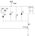

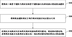
Classifications
-
- H—ELECTRICITY
- H10—SEMICONDUCTOR DEVICES; ELECTRIC SOLID-STATE DEVICES NOT OTHERWISE PROVIDED FOR
- H10W—GENERIC PACKAGES, INTERCONNECTIONS, CONNECTORS OR OTHER CONSTRUCTIONAL DETAILS OF DEVICES COVERED BY CLASS H10
- H10W90/00—Package configurations
-
- H—ELECTRICITY
- H01—ELECTRIC ELEMENTS
- H01H—ELECTRIC SWITCHES; RELAYS; SELECTORS; EMERGENCY PROTECTIVE DEVICES
- H01H47/00—Circuit arrangements not adapted to a particular application of the relay and designed to obtain desired operating characteristics or to provide energising current
- H01H47/002—Monitoring or fail-safe circuits
-
- H—ELECTRICITY
- H01—ELECTRIC ELEMENTS
- H01H—ELECTRIC SWITCHES; RELAYS; SELECTORS; EMERGENCY PROTECTIVE DEVICES
- H01H47/00—Circuit arrangements not adapted to a particular application of the relay and designed to obtain desired operating characteristics or to provide energising current
- H01H47/02—Circuit arrangements not adapted to a particular application of the relay and designed to obtain desired operating characteristics or to provide energising current for modifying the operation of the relay
-
- H—ELECTRICITY
- H02—GENERATION; CONVERSION OR DISTRIBUTION OF ELECTRIC POWER
- H02H—EMERGENCY PROTECTIVE CIRCUIT ARRANGEMENTS
- H02H9/00—Emergency protective circuit arrangements for limiting excess current or voltage without disconnection
- H02H9/04—Emergency protective circuit arrangements for limiting excess current or voltage without disconnection responsive to excess voltage
- H02H9/041—Emergency protective circuit arrangements for limiting excess current or voltage without disconnection responsive to excess voltage using a short-circuiting device
-
- H—ELECTRICITY
- H10—SEMICONDUCTOR DEVICES; ELECTRIC SOLID-STATE DEVICES NOT OTHERWISE PROVIDED FOR
- H10W—GENERIC PACKAGES, INTERCONNECTIONS, CONNECTORS OR OTHER CONSTRUCTIONAL DETAILS OF DEVICES COVERED BY CLASS H10
- H10W70/00—Package substrates; Interposers; Redistribution layers [RDL]
- H10W70/40—Leadframes
- H10W70/481—Leadframes for devices being provided for in groups H10D8/00 - H10D48/00
-
- H—ELECTRICITY
- H10—SEMICONDUCTOR DEVICES; ELECTRIC SOLID-STATE DEVICES NOT OTHERWISE PROVIDED FOR
- H10W—GENERIC PACKAGES, INTERCONNECTIONS, CONNECTORS OR OTHER CONSTRUCTIONAL DETAILS OF DEVICES COVERED BY CLASS H10
- H10W74/00—Encapsulations, e.g. protective coatings
- H10W74/01—Manufacture or treatment
-
- H—ELECTRICITY
- H10—SEMICONDUCTOR DEVICES; ELECTRIC SOLID-STATE DEVICES NOT OTHERWISE PROVIDED FOR
- H10W—GENERIC PACKAGES, INTERCONNECTIONS, CONNECTORS OR OTHER CONSTRUCTIONAL DETAILS OF DEVICES COVERED BY CLASS H10
- H10W74/00—Encapsulations, e.g. protective coatings
- H10W74/10—Encapsulations, e.g. protective coatings characterised by their shape or disposition
- H10W74/111—Encapsulations, e.g. protective coatings characterised by their shape or disposition the semiconductor body being completely enclosed
-
- H—ELECTRICITY
- H10—SEMICONDUCTOR DEVICES; ELECTRIC SOLID-STATE DEVICES NOT OTHERWISE PROVIDED FOR
- H10W—GENERIC PACKAGES, INTERCONNECTIONS, CONNECTORS OR OTHER CONSTRUCTIONAL DETAILS OF DEVICES COVERED BY CLASS H10
- H10W90/00—Package configurations
- H10W90/811—Multiple chips on leadframes
-
- H—ELECTRICITY
- H10—SEMICONDUCTOR DEVICES; ELECTRIC SOLID-STATE DEVICES NOT OTHERWISE PROVIDED FOR
- H10W—GENERIC PACKAGES, INTERCONNECTIONS, CONNECTORS OR OTHER CONSTRUCTIONAL DETAILS OF DEVICES COVERED BY CLASS H10
- H10W95/00—Packaging processes not covered by the other groups of this subclass
-
- H—ELECTRICITY
- H10—SEMICONDUCTOR DEVICES; ELECTRIC SOLID-STATE DEVICES NOT OTHERWISE PROVIDED FOR
- H10W—GENERIC PACKAGES, INTERCONNECTIONS, CONNECTORS OR OTHER CONSTRUCTIONAL DETAILS OF DEVICES COVERED BY CLASS H10
- H10W72/00—Interconnections or connectors in packages
- H10W72/071—Connecting or disconnecting
- H10W72/073—Connecting or disconnecting of die-attach connectors
- H10W72/07351—Connecting or disconnecting of die-attach connectors characterised by changes in properties of the die-attach connectors during connecting
- H10W72/07354—Connecting or disconnecting of die-attach connectors characterised by changes in properties of the die-attach connectors during connecting changes in dispositions
-
- H—ELECTRICITY
- H10—SEMICONDUCTOR DEVICES; ELECTRIC SOLID-STATE DEVICES NOT OTHERWISE PROVIDED FOR
- H10W—GENERIC PACKAGES, INTERCONNECTIONS, CONNECTORS OR OTHER CONSTRUCTIONAL DETAILS OF DEVICES COVERED BY CLASS H10
- H10W72/00—Interconnections or connectors in packages
- H10W72/30—Die-attach connectors
- H10W72/341—Dispositions of die-attach connectors, e.g. layouts
- H10W72/347—Dispositions of multiple die-attach connectors
-
- H—ELECTRICITY
- H10—SEMICONDUCTOR DEVICES; ELECTRIC SOLID-STATE DEVICES NOT OTHERWISE PROVIDED FOR
- H10W—GENERIC PACKAGES, INTERCONNECTIONS, CONNECTORS OR OTHER CONSTRUCTIONAL DETAILS OF DEVICES COVERED BY CLASS H10
- H10W74/00—Encapsulations, e.g. protective coatings
-
- H—ELECTRICITY
- H10—SEMICONDUCTOR DEVICES; ELECTRIC SOLID-STATE DEVICES NOT OTHERWISE PROVIDED FOR
- H10W—GENERIC PACKAGES, INTERCONNECTIONS, CONNECTORS OR OTHER CONSTRUCTIONAL DETAILS OF DEVICES COVERED BY CLASS H10
- H10W90/00—Package configurations
- H10W90/701—Package configurations characterised by the relative positions of pads or connectors relative to package parts
- H10W90/731—Package configurations characterised by the relative positions of pads or connectors relative to package parts of die-attach connectors
- H10W90/732—Package configurations characterised by the relative positions of pads or connectors relative to package parts of die-attach connectors between stacked chips
-
- H—ELECTRICITY
- H10—SEMICONDUCTOR DEVICES; ELECTRIC SOLID-STATE DEVICES NOT OTHERWISE PROVIDED FOR
- H10W—GENERIC PACKAGES, INTERCONNECTIONS, CONNECTORS OR OTHER CONSTRUCTIONAL DETAILS OF DEVICES COVERED BY CLASS H10
- H10W90/00—Package configurations
- H10W90/701—Package configurations characterised by the relative positions of pads or connectors relative to package parts
- H10W90/731—Package configurations characterised by the relative positions of pads or connectors relative to package parts of die-attach connectors
- H10W90/736—Package configurations characterised by the relative positions of pads or connectors relative to package parts of die-attach connectors between a chip and a stacked lead frame, conducting package substrate or heat sink
Landscapes
- Emergency Protection Circuit Devices (AREA)
Abstract
Description
| 标号 | 名称 | 标号 | 名称 |
| 100 | 连接片 | 203 | 第一焊片 |
| 200 | 芯片组件 | 204 | 第二焊片 |
| 300 | 塑封部 | 205 | 第三焊片 |
| 201 | 二极管芯片 | 206 | 反压抑制芯片 |
| 202 | 齐纳二极管芯片 | 207 | 第四焊片 |
| 无续流 | 二极管 | 电阻1.5kΩ | 本实施例器件 | TVS | |
| 关断时间 | 1.10ms 最小 | 6.32ms 5.8倍 | 2.61ms 2.3倍 | 1.71ms 1.55倍 | 1.65ms 1.5倍 |
| 反向钳位 | 378V (200-400V随机) | 1.64V (恒定) | 62.40V (随电源电压变化) | 22.4V (恒定) | 32.4V (恒定) |
| 线圈自激正压(欠阻尼) | 142V | 无 | 30.2V | 无 | 22.80V |
| 正向功率 | 无 | 无 | 有,会增加驱动功率 | 无 | 高于设定值时烧毁 |
| 经济性 | …… | 较低 | 较低,配备驱动用高压开关成本高 | 低 | 较高 |
| 集成难度 | …… | SMB封装,小体积,易集成 | 5*1206封装 体积大,多器件,不易集成 | SMB封装,小体积 ,易集成 | SMC封装,体积大,不易集成 |
Claims (9)
Priority Applications (1)
| Application Number | Priority Date | Filing Date | Title |
|---|---|---|---|
| CN202210632568.XA CN114709199B (zh) | 2022-06-07 | 2022-06-07 | 继电器反压抑制模块封装结构、封装方法及续流电路 |
Applications Claiming Priority (1)
| Application Number | Priority Date | Filing Date | Title |
|---|---|---|---|
| CN202210632568.XA CN114709199B (zh) | 2022-06-07 | 2022-06-07 | 继电器反压抑制模块封装结构、封装方法及续流电路 |
Publications (2)
| Publication Number | Publication Date |
|---|---|
| CN114709199A CN114709199A (zh) | 2022-07-05 |
| CN114709199B true CN114709199B (zh) | 2022-11-01 |
Family
ID=82178077
Family Applications (1)
| Application Number | Title | Priority Date | Filing Date |
|---|---|---|---|
| CN202210632568.XA Active CN114709199B (zh) | 2022-06-07 | 2022-06-07 | 继电器反压抑制模块封装结构、封装方法及续流电路 |
Country Status (1)
| Country | Link |
|---|---|
| CN (1) | CN114709199B (zh) |
Citations (6)
| Publication number | Priority date | Publication date | Assignee | Title |
|---|---|---|---|---|
| CN103427409A (zh) * | 2013-08-20 | 2013-12-04 | 绍兴旭昌科技企业有限公司 | 一种浪涌保护器 |
| CN204045599U (zh) * | 2014-09-04 | 2014-12-24 | 山东沂光电子股份有限公司 | 一种双芯片高反压塑封功率二极管 |
| CN206370420U (zh) * | 2017-01-12 | 2017-08-01 | 广东百圳君耀电子有限公司 | 功率型贴片半导体元件 |
| CN210640241U (zh) * | 2019-12-17 | 2020-05-29 | 上海维安半导体有限公司 | 一种模块化封装半导体防浪涌器件 |
| CN211266459U (zh) * | 2019-12-10 | 2020-08-14 | 恒大新能源技术(深圳)有限公司 | 保护电路和开关器件控制电路 |
| CN213635977U (zh) * | 2020-09-22 | 2021-07-06 | 伯恩半导体(深圳)有限公司 | 一种多芯片叠片的贴片二极管封装结构 |
Family Cites Families (5)
| Publication number | Priority date | Publication date | Assignee | Title |
|---|---|---|---|---|
| CN107293597A (zh) * | 2016-04-11 | 2017-10-24 | 苏州锝耀电子有限公司 | 表面贴装整流器件 |
| CN106783783A (zh) * | 2017-01-12 | 2017-05-31 | 广东百圳君耀电子有限公司 | 功率型贴片半导体元件 |
| CN107393822A (zh) * | 2017-07-17 | 2017-11-24 | 中国振华集团永光电子有限公司(国营第八七三厂) | 一种具有瞬态电压抑制和整流功能的玻璃钝化续流二极管的制造方法 |
| CN108461459A (zh) * | 2018-04-02 | 2018-08-28 | 日照鲁光电子科技有限公司 | 一种负极对接双向整流二极管及其制造工艺 |
| CN213635971U (zh) * | 2020-09-22 | 2021-07-06 | 伯恩半导体(深圳)有限公司 | 一种带有芯片模组的贴片二极管封装结构 |
-
2022
- 2022-06-07 CN CN202210632568.XA patent/CN114709199B/zh active Active
Patent Citations (6)
| Publication number | Priority date | Publication date | Assignee | Title |
|---|---|---|---|---|
| CN103427409A (zh) * | 2013-08-20 | 2013-12-04 | 绍兴旭昌科技企业有限公司 | 一种浪涌保护器 |
| CN204045599U (zh) * | 2014-09-04 | 2014-12-24 | 山东沂光电子股份有限公司 | 一种双芯片高反压塑封功率二极管 |
| CN206370420U (zh) * | 2017-01-12 | 2017-08-01 | 广东百圳君耀电子有限公司 | 功率型贴片半导体元件 |
| CN211266459U (zh) * | 2019-12-10 | 2020-08-14 | 恒大新能源技术(深圳)有限公司 | 保护电路和开关器件控制电路 |
| CN210640241U (zh) * | 2019-12-17 | 2020-05-29 | 上海维安半导体有限公司 | 一种模块化封装半导体防浪涌器件 |
| CN213635977U (zh) * | 2020-09-22 | 2021-07-06 | 伯恩半导体(深圳)有限公司 | 一种多芯片叠片的贴片二极管封装结构 |
Also Published As
| Publication number | Publication date |
|---|---|
| CN114709199A (zh) | 2022-07-05 |
Similar Documents
| Publication | Publication Date | Title |
|---|---|---|
| JP2692765B2 (ja) | ダイオード及びigbtとの並列回路とそのモジュール及びそれを用いた電力変換装置 | |
| US11539361B2 (en) | Semiconductor device signal transmission circuit for drive-control, method of controlling semiconductor device signal transmission circuit for drive-control, semiconductor device, power conversion device, and electric system for railway vehicle | |
| CN104283448B (zh) | 电力变换装置 | |
| US11631974B2 (en) | Snubber circuit and power semiconductor module with snubber circuit | |
| CN101496270A (zh) | 具有针对线感应瞬态的瞬态电压抑制设备的开关模式电源以及用于抑制驱动器级中的多余振荡的机制 | |
| JP3915455B2 (ja) | 半導体電力変換装置 | |
| CN114709199A (zh) | 继电器反压抑制模块封装结构、封装方法及续流电路 | |
| JP4631179B2 (ja) | 半導体装置およびこれを用いたインバータ装置 | |
| US10002699B2 (en) | Electromagnetic coil driving control device | |
| CN1263378A (zh) | 变换器装置 | |
| CN117977992B (zh) | 开关电路、功率集成模块及车辆 | |
| JP2009273272A (ja) | インバータモジュール | |
| JPH077924A (ja) | スナバユニット | |
| CN107592103A (zh) | 一种微秒级电子开关装置 | |
| CN220753430U (zh) | 集成器件、电子电路、电路板和空调器 | |
| CN214507028U (zh) | 一种sic-mosfet驱动保护电路 | |
| CN209641656U (zh) | 功率组件以及电动车 | |
| CN109768036A (zh) | 一种具有回流导电层的功率模块 | |
| CN103051159A (zh) | 电力电子装置及其混合功率模块、混合功率模块的形成方法 | |
| JP2023140611A (ja) | 半導体装置、電力変換装置 | |
| CN207442690U (zh) | 一种变频器igbt控制电路、使用该控制电路的压缩机和空调 | |
| CN223309584U (zh) | 一种低压降防反执行电路 | |
| CN114851887B (zh) | 充电桩及其功率分配单元 | |
| CN220896670U (zh) | 一种dpim功率开关模块 | |
| CN213661443U (zh) | 一种晶闸管的驱动装置 |
Legal Events
| Date | Code | Title | Description |
|---|---|---|---|
| PB01 | Publication | ||
| PB01 | Publication | ||
| SE01 | Entry into force of request for substantive examination | ||
| SE01 | Entry into force of request for substantive examination | ||
| CB03 | Change of inventor or designer information | ||
| CB03 | Change of inventor or designer information |
Inventor after: Zhang Ruguang Inventor after: Zhou Kangping Inventor after: Tang Jiaan Inventor after: Nie Defu Inventor after: Zheng Handong Inventor after: Nong Jinyan Inventor after: Pan Haisheng Inventor before: Zhang Ruguang Inventor before: Zhou Kangping Inventor before: Tang Jiaan Inventor before: Nie Defu Inventor before: Zheng Handong Inventor before: Nong Jinyan Inventor before: Pan Haisheng |
|
| GR01 | Patent grant | ||
| GR01 | Patent grant |