CN114223042A - Radio wave absorber film and method for producing same - Google Patents
Radio wave absorber film and method for producing same Download PDFInfo
- Publication number
- CN114223042A CN114223042A CN202080057040.3A CN202080057040A CN114223042A CN 114223042 A CN114223042 A CN 114223042A CN 202080057040 A CN202080057040 A CN 202080057040A CN 114223042 A CN114223042 A CN 114223042A
- Authority
- CN
- China
- Prior art keywords
- radio wave
- wave absorber
- absorbing layer
- wave absorbing
- absorber film
- Prior art date
- Legal status (The legal status is an assumption and is not a legal conclusion. Google has not performed a legal analysis and makes no representation as to the accuracy of the status listed.)
- Pending
Links
Images


Classifications
-
- H—ELECTRICITY
- H05—ELECTRIC TECHNIQUES NOT OTHERWISE PROVIDED FOR
- H05K—PRINTED CIRCUITS; CASINGS OR CONSTRUCTIONAL DETAILS OF ELECTRIC APPARATUS; MANUFACTURE OF ASSEMBLAGES OF ELECTRICAL COMPONENTS
- H05K9/00—Screening of apparatus or components against electric or magnetic fields
- H05K9/0073—Shielding materials
- H05K9/0075—Magnetic shielding materials
-
- H—ELECTRICITY
- H01—ELECTRIC ELEMENTS
- H01Q—ANTENNAS, i.e. RADIO AERIALS
- H01Q17/00—Devices for absorbing waves radiated from an antenna; Combinations of such devices with active antenna elements or systems
-
- B—PERFORMING OPERATIONS; TRANSPORTING
- B05—SPRAYING OR ATOMISING IN GENERAL; APPLYING FLUENT MATERIALS TO SURFACES, IN GENERAL
- B05D—PROCESSES FOR APPLYING FLUENT MATERIALS TO SURFACES, IN GENERAL
- B05D7/00—Processes, other than flocking, specially adapted for applying liquids or other fluent materials to particular surfaces or for applying particular liquids or other fluent materials
- B05D7/24—Processes, other than flocking, specially adapted for applying liquids or other fluent materials to particular surfaces or for applying particular liquids or other fluent materials for applying particular liquids or other fluent materials
-
- B—PERFORMING OPERATIONS; TRANSPORTING
- B32—LAYERED PRODUCTS
- B32B—LAYERED PRODUCTS, i.e. PRODUCTS BUILT-UP OF STRATA OF FLAT OR NON-FLAT, e.g. CELLULAR OR HONEYCOMB, FORM
- B32B7/00—Layered products characterised by the relation between layers; Layered products characterised by the relative orientation of features between layers, or by the relative values of a measurable parameter between layers, i.e. products comprising layers having different physical, chemical or physicochemical properties; Layered products characterised by the interconnection of layers
- B32B7/02—Physical, chemical or physicochemical properties
- B32B7/025—Electric or magnetic properties
-
- H—ELECTRICITY
- H01—ELECTRIC ELEMENTS
- H01F—MAGNETS; INDUCTANCES; TRANSFORMERS; SELECTION OF MATERIALS FOR THEIR MAGNETIC PROPERTIES
- H01F1/00—Magnets or magnetic bodies characterised by the magnetic materials therefor; Selection of materials for their magnetic properties
- H01F1/01—Magnets or magnetic bodies characterised by the magnetic materials therefor; Selection of materials for their magnetic properties of inorganic materials
- H01F1/03—Magnets or magnetic bodies characterised by the magnetic materials therefor; Selection of materials for their magnetic properties of inorganic materials characterised by their coercivity
- H01F1/032—Magnets or magnetic bodies characterised by the magnetic materials therefor; Selection of materials for their magnetic properties of inorganic materials characterised by their coercivity of hard-magnetic materials
- H01F1/10—Magnets or magnetic bodies characterised by the magnetic materials therefor; Selection of materials for their magnetic properties of inorganic materials characterised by their coercivity of hard-magnetic materials non-metallic substances, e.g. ferrites, e.g. [(Ba,Sr)O(Fe2O3)6] ferrites with hexagonal structure
- H01F1/11—Magnets or magnetic bodies characterised by the magnetic materials therefor; Selection of materials for their magnetic properties of inorganic materials characterised by their coercivity of hard-magnetic materials non-metallic substances, e.g. ferrites, e.g. [(Ba,Sr)O(Fe2O3)6] ferrites with hexagonal structure in the form of particles
- H01F1/113—Magnets or magnetic bodies characterised by the magnetic materials therefor; Selection of materials for their magnetic properties of inorganic materials characterised by their coercivity of hard-magnetic materials non-metallic substances, e.g. ferrites, e.g. [(Ba,Sr)O(Fe2O3)6] ferrites with hexagonal structure in the form of particles in a bonding agent
- H01F1/117—Flexible bodies
-
- H—ELECTRICITY
- H01—ELECTRIC ELEMENTS
- H01F—MAGNETS; INDUCTANCES; TRANSFORMERS; SELECTION OF MATERIALS FOR THEIR MAGNETIC PROPERTIES
- H01F3/00—Cores, Yokes, or armatures
- H01F3/02—Cores, Yokes, or armatures made from sheets
-
- H—ELECTRICITY
- H01—ELECTRIC ELEMENTS
- H01Q—ANTENNAS, i.e. RADIO AERIALS
- H01Q17/00—Devices for absorbing waves radiated from an antenna; Combinations of such devices with active antenna elements or systems
- H01Q17/002—Devices for absorbing waves radiated from an antenna; Combinations of such devices with active antenna elements or systems using short elongated elements as dissipative material, e.g. metallic threads or flake-like particles
-
- H—ELECTRICITY
- H05—ELECTRIC TECHNIQUES NOT OTHERWISE PROVIDED FOR
- H05K—PRINTED CIRCUITS; CASINGS OR CONSTRUCTIONAL DETAILS OF ELECTRIC APPARATUS; MANUFACTURE OF ASSEMBLAGES OF ELECTRICAL COMPONENTS
- H05K9/00—Screening of apparatus or components against electric or magnetic fields
- H05K9/0073—Shielding materials
- H05K9/0081—Electromagnetic shielding materials, e.g. EMI, RFI shielding
-
- B—PERFORMING OPERATIONS; TRANSPORTING
- B05—SPRAYING OR ATOMISING IN GENERAL; APPLYING FLUENT MATERIALS TO SURFACES, IN GENERAL
- B05D—PROCESSES FOR APPLYING FLUENT MATERIALS TO SURFACES, IN GENERAL
- B05D2430/00—Component used as a filler in the composition
-
- H—ELECTRICITY
- H01—ELECTRIC ELEMENTS
- H01F—MAGNETS; INDUCTANCES; TRANSFORMERS; SELECTION OF MATERIALS FOR THEIR MAGNETIC PROPERTIES
- H01F1/00—Magnets or magnetic bodies characterised by the magnetic materials therefor; Selection of materials for their magnetic properties
- H01F1/01—Magnets or magnetic bodies characterised by the magnetic materials therefor; Selection of materials for their magnetic properties of inorganic materials
- H01F1/03—Magnets or magnetic bodies characterised by the magnetic materials therefor; Selection of materials for their magnetic properties of inorganic materials characterised by their coercivity
- H01F1/12—Magnets or magnetic bodies characterised by the magnetic materials therefor; Selection of materials for their magnetic properties of inorganic materials characterised by their coercivity of soft-magnetic materials
- H01F1/34—Magnets or magnetic bodies characterised by the magnetic materials therefor; Selection of materials for their magnetic properties of inorganic materials characterised by their coercivity of soft-magnetic materials non-metallic substances, e.g. ferrites
- H01F1/342—Oxides
- H01F1/344—Ferrites, e.g. having a cubic spinel structure (X2+O)(Y23+O3), e.g. magnetite Fe3O4
- H01F1/348—Hexaferrites with decreased hardness or anisotropy, i.e. with increased permeability in the microwave (GHz) range, e.g. having a hexagonal crystallographic structure
Abstract
The invention provides a radio wave absorber film which is thin and has excellent radio wave absorption performance, and a manufacturing method of the radio wave absorber film. In the radio wave absorber film formed on the base layer, the radio wave absorber layer includes a magnetic material and a binder resin, and an aromatic ester-urethane copolymer is used as the binder resin. The glass transition temperature of the binder resin is preferably 100 ℃ or lower, and more preferably 0 ℃ or lower. The magnetic material is preferably at least one selected from the group consisting of an epsilon-type iron oxide, a barium ferrite magnetic material, and a strontium ferrite magnetic material.
Description
Technical Field
The present invention relates to a radio wave absorber film having excellent radio wave absorbing performance and a method for producing the same.
Background
High-frequency band radio waves are widely used in various information communication systems such as mobile phones, wireless LANs, ETC systems, highway traffic systems, automobile driving assistance road systems, and satellite broadcasts. However, the expanded use of radio waves in a high frequency band may cause malfunction, and the like of electronic equipment due to interference between electronic components. As a countermeasure against such a problem, a method of absorbing unnecessary radio waves by a radio wave absorber is adopted.
Therefore, in a radar or the like using radio waves in a high frequency band, a radio wave absorber is used in order to reduce the influence of unnecessary radio waves that should not be received.
In order to meet such a demand, various radio wave absorbers capable of absorbing radio waves in a high frequency band have been proposed. As a specific example, a radio wave absorbing sheet containing a carbon nanocoil and a resin is known (for example, patent document 1).
In the application of radio waves in a high frequency band, a vehicle driving support system is being studied. In the vehicle-mounted radar for detecting the inter-vehicle distance or the like, the vehicle driving support system uses a radio wave in a 76GHz band. It is also expected that the use of radio waves in a high frequency band of, for example, 100GHz or more will be expanded in various applications, not limited to the driving support system of the automobile. Therefore, a radio wave absorber capable of absorbing radio waves of a frequency band of 76GHz or higher is desired.
In order to meet such a demand, as a radio wave absorber capable of absorbing radio waves well in a wide range of a high frequency band, for example, a radio wave absorber having a radio wave absorbing layer containing ∈ -Fe is proposed2O3Magnetic crystals of iron oxide (for example, patent document 2 and non-patent documents 1 to 3).
Documents of the prior art
Patent document
Patent document 1: japanese patent laid-open publication No. 2009-
Patent document 2: japanese patent laid-open No. 2008-277726
Non-patent document
Non-patent document 1: namai, s.sakurai, m.nakajima, t.suemoto, k.matsumoto, m.goto, s.sasaki, and s.ohkoshi, j.am.chem.soc., 131, 1170-.
Non-patent document 2: namai, m.yoshikiyo, k.yamada, s.sakurai, t.goto, t.yoshida, T Miyazaki, m.nakajima, t.suemoto, h.tokoro, and s.ohkoshi, Nature Communications, 3, 1035/1-6(2012).
Non-patent document 3: s.ohkoshi, s.kuroki, s.sakurai, k.matsumoto, k.sato, and s.sasaki, angelw.chem.int.ed., 46, 8392-.
Disclosure of Invention
Problems to be solved by the invention
However, it is strongly required to achieve both a thinner film and a better radio wave absorption performance for such a radio wave absorption sheet described in patent document 1.
The present invention has been made in view of the above-mentioned problems of the prior art, and an object thereof is to provide a radio wave absorber film which is made thin and has excellent radio wave absorption performance, and a method for manufacturing the radio wave absorber film.
Means for solving the problems
The present inventors have found that the above problems can be solved by using an aromatic ester-urethane copolymer as a binder resin in a radio wave absorber film formed on a base layer, the radio wave absorber film including a magnetic material and the binder resin in the radio wave absorber layer, and have completed the present invention.
The invention according to claim 1 is a radio wave absorber film comprising a radio wave absorbing layer formed on a base layer,
the electric wave absorbing layer contains a magnetic body and a binder resin,
the binder resin comprises an aromatic ester-urethane copolymer.
The 2 nd aspect of the present invention is a method for manufacturing a radio wave absorber film, including the following radio wave absorber layer forming step: coating a paste containing a magnetic material and a binder resin on the base material layer to form a coating film, drying the coating film to form a radio wave absorbing layer,
the binder resin comprises an aromatic ester-urethane copolymer.
ADVANTAGEOUS EFFECTS OF INVENTION
According to the present invention, a radio wave absorber film having a reduced thickness and excellent radio wave absorption performance, and a method for producing the radio wave absorber film can be provided.
Drawings
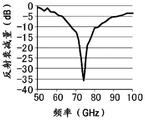
FIG. 1 is a graph showing the reflection attenuation of the radio wave absorber film of example 1.
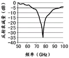
FIG. 2 is a graph showing the reflection attenuation of the radio wave absorber film of example 2.
FIG. 3 is a graph showing the reflection attenuation of the radio wave absorber film of example 3.
FIG. 4 is a graph showing the reflection attenuation of the radio wave absorber film of example 4.
FIG. 5 is a graph showing the reflection attenuation of the radio wave absorber film of comparative example 1.
Detailed Description
The present invention is not limited to the following embodiments, and can be carried out with appropriate modifications within the scope of the object of the present invention.
In the present specification, "-" represents "or more and" or "less" unless otherwise specified.
< radio wave absorber film >)
The radio wave absorbing film includes a radio wave absorbing layer formed on a base layer. The radio wave absorbing layer includes a magnetic body and a binder resin. The binder resin comprises an aromatic ester-urethane copolymer.
By containing a magnetic material and an aromatic ester-urethane copolymer as a binder resin in the radio wave absorbing layer, a radio wave absorbing film having excellent radio wave absorbing characteristics even in the form of a thin film can be produced.
In terms of more reliably absorbing high-frequency waves in the millimeter waveband or more, a frequency band of 30 gigahertz (GHz) or more (preferably 30GHz to 300GHz, more preferably 40GHz to 200 GHz) is preferable for the radio wave absorber film. It is preferable that a peak having an absolute value of 30dB or more is present in the reflection attenuation measured from the side having the radio wave absorbing layer.
Unless otherwise specified, the transmission attenuation value is a value measured under the conditions of measurement in examples described below.
The shape of the radio wave absorber film may have a curved surface or may be constituted by only a flat surface, and is preferably a flat plate.
From the viewpoint of making the film thin or compact without impairing the effects of the present invention, the thickness of the radio wave absorber film is preferably 1000 μm or less, more preferably 900 μm or less, still more preferably 450 μm or less, and particularly preferably 200 μm or less.
The thickness of the radio wave absorber film may be uniform or non-uniform.
< radio wave absorbing layer >
As described above, the electric wave absorbing layer contains a magnetic body and a binder resin. The binder resin comprises an aromatic ester-urethane copolymer.
The thickness of the radio wave absorbing layer is not particularly limited as long as the object of the present invention is not impaired. The thickness of the radio wave absorbing layer is preferably 100 μm or less, more preferably 50 μm or less, from the viewpoint of the balance between the reduction in thickness of the radio wave absorbing film and the radio wave absorbing performance.
The lower limit of the thickness of the radio wave absorbing layer is not particularly limited as long as the effect of the present invention is not impaired, and examples thereof include 1 μm or more and 10 μm or more.
The thickness of the radio wave absorbing layer may be uniform or non-uniform.
Hereinafter, the essential or optional configuration of the radio wave absorbing layer will be described.
[ Binder resin ]
The radio wave absorbing layer includes a magnetic body and a binder resin. The binder resin comprises an aromatic ester-urethane copolymer. By using the aromatic ester-urethane copolymer as the binder resin, a radio wave absorber film can be produced which has magnetic bodies well dispersed in the binder resin and which exhibits excellent radio wave absorption characteristics even when it is thin.
In addition, when an aromatic ester-urethane copolymer is used as the binder resin, crack resistance and low warpage properties at the time of bending or cutting can be imparted to the radio wave absorbing layer.
The glass transition temperature of the binder resin is preferably 100 ℃ or lower, and more preferably 0 ℃ or lower, from the viewpoint of satisfactory crack resistance and low warpage of the radio wave absorbing layer. Therefore, the glass transition temperature of the aromatic ester-urethane copolymer is also preferably 100 ℃ or lower, and more preferably 0 ℃ or lower.
The aromatic ester-urethane copolymer is a copolymer containing an ester bond (-CO-O-) and a urethane bond (-NH-CO-O-) and containing an aromatic group in the main chain skeleton.
The aromatic group in the main chain skeleton may be an aromatic hydrocarbon group or a heterocyclic aromatic group, and is preferably an aromatic hydrocarbon group. The aromatic ester-urethane copolymer may be a random copolymer in which an ester bond and a urethane bond are randomly introduced into a molecular chain, or may be a block copolymer including 1 or more ester blocks and 1 or more urethane blocks.
The method for producing the aromatic ester-urethane copolymer is not particularly limited. Typically, the aromatic ester-urethane copolymer can be produced by: at least one monomer selected from the group consisting of a diol component (a1), a dicarboxylic acid (a2), a hydroxycarboxylic acid component (a3), and a diisocyanate component (a4) is polymerized in one stage or in multiple stages.
The dicarboxylic acid component (a2) and the hydroxycarboxylic acid component (a3) can be used as ester derivatives such as methyl esters and ethyl esters, esters such as carboxylic acid halides (carboxylic acid chlorides), and derivatives with carbamate-forming properties.
The monomer used for producing the aromatic ester-urethane copolymer is preferably a compound in which 2 functional groups selected from the group consisting of a hydroxyl group, a carboxyl group, and an isocyanate group are bonded to a 2-valent hydrocarbon group having an unbranched structure.
Examples of the 2-valent hydrocarbon group having an unbranched structure include an alkylene group, an alkenylene group, an alkynylene group, an arylene group, and a combination of these groups. The alkylene, alkenylene, and alkynylene groups are preferably linear structures.
When the 2-valent hydrocarbon group having an unbranched structure is an alkylene group, an alkenylene group, or an alkynylene group, the number of carbon atoms of these groups is preferably 1 to 8, more preferably 2 to 6, and still more preferably 2 to 4.
When the 2-valent hydrocarbon group having an unbranched structure is an arylene group, the arylene group is preferably a phenylene group or a naphthylene group, more preferably a phenylene group, and still more preferably a p-phenylene group.
Of the above-described unbranched-structured 2-valent hydrocarbon groups, preferable are alkylene groups, and arylene groups, and combinations of alkylene groups and arylene groups.
Preferable specific examples of the diol component (a1) include ethylene glycol, 1, 3-propanediol, 1, 4-butanediol, neopentyl glycol, 1, 6-hexanediol, 1, 4-cyclohexanedimethanol, and 1, 5-pentanediol.
Preferable specific examples of the dicarboxylic acid (a2) include terephthalic acid, isophthalic acid, 2, 6-naphthalenedicarboxylic acid, 2, 7-naphthalenedicarboxylic acid, 1, 4-cyclohexanedicarboxylic acid, succinic acid, glutaric acid, adipic acid, oxalic acid, malonic acid, and the like.
Preferable specific examples of the hydroxycarboxylic acid component (a3) include 4-hydroxybenzoic acid, 3-hydroxybenzoic acid, 6-hydroxynaphthalene-2-carboxylic acid, glycolic acid, lactic acid, and γ -hydroxybutyric acid.
Preferred specific examples of the diisocyanate component (a4) include ethylene diisocyanate, trimethylene diisocyanate, tetramethylene diisocyanate, hexamethylene diisocyanate, isophorone diisocyanate, m-xylylene diisocyanate, p-xylylene diisocyanate, toluene diisocyanate, 4' -diphenylmethane diisocyanate, and 1, 5-naphthalene diisocyanate.
The weight average molecular weight (Mw) of the aromatic ester-urethane copolymer is preferably 5000 to 500000, more preferably 10000 to 200000. In the specification of the present application, the weight average molecular weight (Mw) refers to a weight average molecular weight in terms of polystyrene measured by GPC.
Examples of commercially available products of the aromatic ester-urethane copolymer include Vylon Series (trade name) (manufactured by toyobo co., ltd.). More specifically, Vylon UR-1400, Vylon UR-1410, Vylon UR-1700, Vylon UR-2300, Vylon UR-3200, Vylon UR-3210, Vylon UR-3500, Vylon UR-6100, Vylon UR-8300, Vylon UR-8700, and the like can be preferably used.
The binder resin may contain other resins than the aromatic ester-urethane copolymer within a range not hindering the object of the present invention. The type of the other resin is not particularly limited as long as the object of the present invention is not impaired. The other resin may be an elastic material such as an elastomer or rubber. The other resin may be a thermoplastic resin or a curable resin. When the other resin is a curable resin, the curable resin may be a photocurable resin or a thermosetting resin.
Preferable examples of the other resin in the case of a thermoplastic resin include polyacetal resin, polyamide resin, polycarbonate resin, polyester resin (e.g., polybutylene terephthalate, polyethylene terephthalate, or polyarylate), FR-AS resin, FR-ABS resin, AS resin, ABS resin, polyphenylene ether resin, polyphenylene sulfide resin, polysulfone resin, polyethersulfone resin, polyetheretherketone resin, fluorine-based resin, polyimide resin, polyamideimide resin, polyetherimide resin, polybenzoxazole resin, polybenzothiazole resin, polybenzimidazole resin, BT resin, polymethylpentene, ultrahigh-molecular-weight polyethylene, FR-polypropylene, cellulose resin (e.g., methylcellulose, ethylcellulose), (meth) acrylic resin (e.g., polymethacrylate), etc.), And polystyrene, and the like.
Preferred examples of the other resin in the case of being a thermosetting resin include a phenol resin, a melamine resin, an epoxy resin, and an alkyd resin. As the photocurable resin, a resin obtained by photocuring a monomer having an unsaturated bond such as various vinyl monomers or various (meth) acrylates can be used.
Preferable examples of the other resin as the elastic material include olefin-based elastomers, styrene-based elastomers, polyamide-based elastomers, polyester-based elastomers, polyurethane-based elastomers, and the like.
The ratio of the mass of the other resin to the total mass of the binder resin is not particularly limited within a range not hindering the object of the present invention. In view of easily obtaining a radio wave absorber film having desired performance, the ratio of the mass of the other resin to the total mass of the binder resin is, for example, preferably 20 mass% or less, more preferably 10 mass% or less, still more preferably 5 mass% or less, still more preferably 1 mass% or less, and most preferably 0 mass%.
The content of the binder resin in the radio wave absorbing layer is not particularly limited within a range not to impair the object of the present invention. The content of the binder resin is preferably 5 mass% or more and 30 mass% or less, and more preferably 10 mass% or more and 25 mass% or less, with respect to the mass of the solid content of the radio wave absorbing layer.
[ magnetic body ]
The type of the magnetic material is not particularly limited as long as the radio wave absorber film exhibits a desired radio wave absorption property.
The magnetic material is preferably a magnetic material that generates magnetic resonance in a frequency band of 30GHz or more, and more preferably a magnetic material that generates magnetic resonance in a frequency band of 30GHz or more and 300GHz or less, from the viewpoint of absorbing high-frequency waves in the millimeter wave band or more.
The magnetic resonance is based on precession movement when an electron spin in an atom moves in a frequency band of a millimeter wave band or more. Natural magnetic resonance caused by the gyro magnetic effect based on precession motion in a frequency band above the millimeter wave band is preferable.
The magnetic material is not particularly limited as long as it can absorb high-frequency radio waves in a millimeter wave band or more. A preferable magnetic material includes at least one selected from the group consisting of an epsilon-type iron oxide, a barium ferrite magnetic material, and a strontium ferrite magnetic material.
The epsilon-type iron oxide will be explained below.
(Epsilon type iron oxide)
As the epsilon-type iron oxide, it is preferably selected from the group consisting of epsilon-Fe2O3At least one of a crystal having a crystal structure and space group and epsilon-Fe, and a crystal obtained by using the same2O3Is same as ε -Fe2O3A part of Fe sites of the crystal is substituted by an element M other than Fe, and is represented by the formula ε -MxFe2-xO3And x is 0 to 2 (preferably 0 to less than 2). Since such crystals of epsilon-type iron oxide are magnetic crystals, the crystals are sometimes referred to as "magnetic crystals" in the present specification.
With respect to ε -Fe2O3As the crystal, any crystal can be used. As for the crystals described below, it is stated hereinafter that the crystal structure and space group of the crystals and ε -Fe2O3Same, epsilon-Fe2O3A part of Fe sites of the crystal is replaced by an element M other than Fe, and is represented by the formula epsilon-MxFe2-xO3And x is 0 to 2 (preferably 0 to less than 2).
In the present specification, ε -Fe is also used2O3A part of Fe sites of the crystal is replaced by a substitution element MConverted epsilon-MxFe2-xO3Referred to as "M replacing ε -Fe2O3”。
Having epsilon-Fe in the magnetic phase2O3Crystals and/or M replacing epsilon-Fe2O3The particle size of the crystal particles is not particularly limited as long as the object of the present invention is not impaired. For example, particles having magnetic crystals of epsilon-type iron oxide in the magnetic phase, which are produced by a method described below, have an average particle diameter in the range of 5nm to 200nm as measured by a TEM (transmission electron microscope) photograph.
The coefficient of variation (standard deviation of particle diameter/average particle diameter) of the particles of the magnetic crystal having epsilon-type iron oxide in the magnetic layer, which are produced by the method described later, is less than 80%, and the particles are relatively fine and uniform in particle diameter.
In a preferred radio wave absorbing layer, magnetic particles of such epsilon-type iron oxide (i.e., having epsilon-Fe in the magnetic phase) are used2O3Crystals and/or M replacing epsilon-Fe2O3Crystalline particles) is used as a radio wave absorbing material in the radio wave absorbing layer, i.e., a magnetic body. The "magnetic phase" referred to herein is a portion that bears the magnetism of the powder.
So-called "having epsilon-Fe in magnetic phase2O3Crystals and/or M replacing epsilon-Fe2O3Crystal' means that the magnetic phase is composed of epsilon-Fe2O3Crystals and/or M replacing epsilon-Fe2O3The crystal formation includes a case where magnetic crystals, which are inevitable for production, are mixed in the magnetic phase.
The magnetic crystal of the epsilon-type iron oxide may contain a space group, an oxidation state and epsilon-Fe2O3Impurity crystals of iron oxide having different crystals (specifically, alpha-Fe)2O3、γ-Fe2O3FeO and Fe3O4And a crystal in which a part of Fe is replaced with another element) in these crystals.
When the magnetic crystal of the epsilon-type iron oxide contains impurity crystals, epsilon-Fe is preferable2O3And/or M replacing epsilon-Fe2O3The magnetic crystal of (2) is a main phase. That is, in the magnetic crystal of epsilon iron oxide constituting the electric wave absorbing material, epsilon-Fe2O3And/or M replacing epsilon-Fe2O3The ratio of the magnetic crystal of (3) is preferably 50 mol% or more in terms of a molar ratio of the compound.
The presence ratio of crystals can be determined by analysis using the Rietveld method (which is based on an X-ray diffraction pattern). Silica (SiO) formed in the sol-gel process sometimes adheres to the periphery of the magnetic phase2) And the like non-magnetic compounds.
(M for ε -Fe)2O3)
As long as the crystal and space group and epsilon-Fe are satisfied2O3Same, epsilon-Fe2O3A condition that a part of Fe sites of the crystal is replaced by an element M other than Fe, M replacing epsilon-Fe2O3The kind of the element M in (2) is not particularly limited. Replacement of epsilon-Fe by M2O3A plurality of elements M other than Fe may be contained.
Preferable examples of the element M include In, Ga, Al, Sc, Cr, Sm, Yb, Ce, Ru, Rh, Ti, Co, Ni, Mn, Zn, Zr, and Y. Among these, In, Ga, Al, Ti, Co and Rh are preferable. When M is Al, in the range of ε -MxFe2-xO3In the composition represented, x is preferably in the range of, for example, 0 or more and less than 0.8. When M is Ga, x is preferably in the range of, for example, 0 or more and less than 0.8. When M is In, x is preferably In the range of, for example, 0 or more and less than 0.3. When M is Rh, x is preferably in the range of, for example, 0 or more and less than 0.3. When M is Ti or Co, x is preferably in the range of, for example, 0 or more and less than 1.
The frequency at which the amount of radio wave absorption becomes maximum can be adjusted by: replacement of ε -Fe for M2O3At least one of the kind and the amount of substitution of the element M in (b) is adjusted.
Such M replacing ε -Fe2O3The magnetic crystal can be synthesized, for example, by a process combining the reversed micelle method and the sol-gel method and a firing process, which will be described later. In addition, can be determined by Japanese patent laid-open2008-174405, which combines the steps of the direct synthesis method and the sol-gel method, and the firing step, to synthesize M-substituted ε -Fe2O3A magnetic crystal.
Specifically, the substitution of M for ε -Fe can be obtained by using a combination of the reversed micelle method and the sol-gel method and the firing step described in the following documents2O3Magnetic crystal:
Jian Jin,Shin-ichi Ohkoshi and Kazuhito Hashimoto,ADVANCED MATERIALS 2004,16,No.1、January 5,p.48-51;
Shin-ichi Ohkoshi,Shunsuke Sakurai,Jian Jin,Kazuhito Hashimoto,JOURNAL OF APPLiED PHYSICS,97,10K312(2005)、
Shunsuke Sakurai,Jian Jin,Kazuhito Hashimoto and Shin-ichi Ohkoshi,JOURNAL OF THE PHYSICAL SOCIETY OF JAPAN,Vol.74,No.7,July,2005、p.1946-1949;
asuka Namai, Shunsuke Sakurai, Makoto Nakajima, Tohru Suemoto, Kazuyuki Matsumoto, Masahiro Goto, Shinya Sasaki, and Shin-ichi Ohkoshi, Journal of the American Chemical Society, Vol.131, p.1170-1173, 2009; and so on.
In the reverse micelle method, a micelle solution I (raw material micelle) which is a 2-micelle solution containing a surfactant is mixed with a micelle solution II (neutralizer micelle), thereby performing a precipitation reaction of iron hydroxide in the micelle. Next, a silica coating is applied to the surface of the iron hydroxide microparticles produced in the micelle by a sol-gel method. The iron hydroxide particles having a silica coating layer are separated from the liquid, and then subjected to heat treatment in an atmospheric atmosphere at a predetermined temperature (within a range of 700 to 1300 ℃). By this heat treatment, epsilon-Fe can be obtained2O3Particles of crystals.
More specifically, for example, M in place of ε -Fe is produced in the following manner2O3A magnetic crystal.
First, In the aqueous phase of the micellar solution I having n-octane as an oil phase, iron (III) nitrate as an iron source, and M nitrate (aluminum (III) nitrate 9 hydrate In the case of Al, gallium (III) nitrate hydrate In the case of Ga, indium (III) nitrate 3 hydrate In the case of In, titanium (IV) sulfate hydrate and cobalt (II) nitrate 6 hydrate In the case of Ti and Co) as an M element source In which a part of iron is replaced, and a surfactant (for example, cetyltrimethylammonium bromide) are dissolved.
An appropriate amount of nitrate of alkaline earth metal (Ba, Sr, Ca, etc.) may be dissolved in advance in the aqueous phase of the micellar solution I. The nitrate functions as a shape-controlling agent. When alkaline earth metal exists in the liquid, the rodlike M replaces epsilon-Fe2O3Particles of magnetic crystals. In the absence of a shape-controlling agent, nearly spherical shape of M in place of ε -Fe can be obtained2O3Particles of magnetic crystals.
The alkaline earth metal added as a shape-controlling agent may remain in the formed M instead of ε -Fe2O3A surface layer portion of the magnetic crystal. Replacement of ε -Fe with respect to M2O3For the sum of the mass of the substitution element M and the mass of Fe in the magnetic crystal, M substitutes for ε -Fe2O3The mass of the alkaline earth metal in the magnetic crystal is preferably 20 mass% or less, and more preferably 10 mass% or less.
An aqueous ammonia solution was used as the aqueous phase of the micelle solution II containing n-octane as an oil phase.
After the micelle solutions I and II are mixed, a sol-gel method is applied. That is, while adding silane (e.g., tetraethyl orthosilicate) dropwise to the mixed solution of the micelle solution, stirring is continued, and the reaction of producing iron hydroxide or iron hydroxide containing the element M proceeds in the micelle. Thereby, the surface of the precipitated particles of fine iron hydroxide generated in the micelle is coated with silica generated by hydrolysis of silane.
Next, a particle powder obtained by separating silica-coated M element-containing iron hydroxide particles from a liquid, washing and drying the separated particles is charged into a furnace, and heat treatment (firing) is performed in air at a temperature range of 700 ℃ to 1300 ℃ (preferably 900 ℃ to 1200 ℃, and more preferably 950 ℃ to 1150 ℃).
Through the heat placeThereby, an oxidation reaction is performed in the silica coating layer, and fine particles of fine iron hydroxide containing M element are changed into fine M replacing epsilon-Fe2O3The particles of (1).
The presence of the silica coating during the oxidation reaction helps to form space groups with epsilon-Fe2O3Same M replacing ε -Fe2O3Crystalline (rather than alpha-Fe)2O3、γ-Fe2O3Crystals of (b) and functions to prevent particles from sintering to each other. In addition, if an appropriate amount of alkaline earth metal coexists, the particle shape tends to grow into a rod shape.
Further, as described above, by combining the steps of the direct synthesis method and the sol-gel method and the firing step as disclosed in Japanese patent laid-open No. 2008-174405, it is possible to economically synthesize more favorably the M-substituted ε -Fe2O3A magnetic crystal.
Briefly, first, a neutralizing agent such as ammonia is added to a water solvent in which a salt of iron salt having a valence of 3 and a substitution element M (Ga, Al, etc.) is dissolved, while stirring, to thereby produce a precursor composed of a hydroxide of iron (a part of which may be substituted with another element).
Then, a coating layer of silica is formed on the surface of the precursor particles by a sol-gel method. The silica-coated particles are separated from the liquid, and then heat-treated (fired) at a predetermined temperature to obtain M in place of ε -Fe2O3Particles of magnetic crystals.
In the above-mentioned case where M is substituted for ε -Fe2O3In the synthesis of (2), a space group, an oxidation state and ε -Fe may be formed2O3Iron oxide crystals (impurity crystals) having different crystals. In the presence of Fe2O3Among the polymorphic forms (polymorphisms) of different compositions but different crystal structures, the most common is α -Fe2O3And gamma-Fe2O3. Examples of the other iron oxides include FeO and Fe3O4And the like.
When such impurity crystals are contained, the substitution of ε -Fe by M is exhibited as high as possible2O3The crystal characteristics cannot be said to be preferable, but is acceptable within a range not impairing the effects of the present invention.
In addition, M replaces ε -Fe2O3Coercive force H of magnetic crystalcVaries according to the replacement amount of the replacement element M. I.e. by replacing ε -Fe for M2O3The replacement amount of the replacement element M in the magnetic crystal is adjusted, so that the replacement of epsilon-Fe by M can be adjusted2O3Coercive force H of magnetic crystalc。
Specifically, for example, in the case of using Al, Ga or the like as the substitution element M, the more the substitution amount increases, the more ε -Fe is substituted by M2O3Coercive force H of magnetic crystalcThe lower the decrease. On the other hand, in the case of using Rh or the like as the substitution element M, the more the substitution amount increases, the more the substitution amount of M for ε -Fe2O3Coercive force H of magnetic crystalcThe larger the increase.
Easily adjusting the replacement of M to epsilon-Fe according to the replacement amount of the replacement element M2O3Coercive force H of magnetic crystalcIn view of the above, Ga, Al, In, Ti, Co and Rh are preferable as the substitution element M.
Further, the coercive force H is accompaniedcThe frequency of the peak at which the radio wave absorption amount of epsilon-type iron oxide becomes maximum also shifts to the low frequency side or the high frequency side. That is, the frequency of the peak of the radio wave absorption amount can be controlled by the substitution amount of the M element.
In the case of a generally used radio wave absorber, the absorption amount becomes substantially zero when the incident angle and frequency of the radio wave deviate from the design values. On the other hand, when epsilon-type iron oxide is used, radio wave absorption is exhibited in a wide frequency range and radio wave incidence angle even if the value is slightly deviated. Therefore, a radio wave absorbing layer that can absorb radio waves in a wide frequency band can be provided.
The particle size of the epsilon-type iron oxide can be controlled by, for example, adjusting the heat treatment (firing) temperature in the above-described step.
Particles of epsilon-iron oxide having a particle diameter in the range of 5nm to 200nm as an average particle diameter measured by a TEM (transmission electron microscope) photograph can be synthesized by the method combining the reversed micelle method and the sol-gel method described above and the method combining the direct synthesis method and the sol-gel method disclosed in jp 2008-174405 a. The average particle diameter of the epsilon-type iron oxide is more preferably 10nm or more, and still more preferably 20nm or more.
When the average particle size is determined as the number average particle size, the average particle size is calculated by taking the diameter of the particles in the long axis direction observed on the TEM image as the diameter of the particles when the particles of the epsilon-type iron oxide are rod-shaped. The number of particles to be measured in obtaining the average particle diameter is not particularly limited as long as it is a number sufficiently large for calculating the average value, and is preferably 300 or more.
Further, the silica coating applied to the surface of the iron hydroxide fine particles by the sol-gel method may be present in the case where e-Fe is replaced by M after heat treatment (firing)2O3The surface of the magnetic crystal. When a nonmagnetic compound such as silica is present on the surface of the crystal, it is preferable from the viewpoint of improving the handling property, durability, weather resistance and the like of the magnetic crystal.
Preferable examples of the nonmagnetic compound include heat-resistant compounds such as alumina and zirconia in addition to silica.
However, if the amount of the nonmagnetic compound adhering is too large, the particles may be strongly aggregated, which is not preferable.
When the non-magnetic compound is silica, e-Fe is replaced with M2O3For the sum of the mass of the substitution element M and the mass of Fe in the magnetic crystal, M substitutes for ε -Fe2O3The mass of Si in the magnetic crystal is preferably 100 mass% or less.
Replacement of epsilon-Fe by M2O3A part or most of the silica attached to the magnetic crystal can be removed by dipping in an alkaline solution. The amount of silica attached can be adjusted to an arbitrary amount by such a method.
The content of the magnetic material in the radio wave absorption layer is not particularly limited within a range not to hinder the object of the present invention. The content of the magnetic material is preferably 30 mass% or more, more preferably 40 mass% or more, particularly preferably 60 mass% or more, and most preferably 60 mass% or more and 91 mass% or less with respect to the mass of the solid component of the radio wave absorbing layer.
(method of adjusting relative dielectric constant)
The relative permittivity of the radio wave absorbing layer is not particularly limited, but is preferably 6.5 to 65, more preferably 10 to 50, and further preferably 15 to 30. The method for adjusting the relative dielectric constant of the radio wave absorbing layer is not particularly limited. As a method for adjusting the relative dielectric constant of each of the radio wave absorbing layers, a method of containing dielectric powder in the radio wave absorbing layer and adjusting the content of the dielectric powder may be mentioned.
Preferable examples of the dielectric include barium titanate, strontium titanate, calcium titanate, magnesium titanate, bismuth titanate, zirconium titanate, zinc titanate, and titanium dioxide. The electric wave absorbing layer may be a combination of powders containing a plurality of dielectrics.
The particle diameter of the dielectric powder used for adjusting the relative permittivity of the radio wave absorbing layer is not particularly limited as long as the object of the present invention is not hindered. The average particle diameter of the dielectric powder is preferably 1nm to 100nm, more preferably 5nm to 50 nm. Here, the average particle diameter of the dielectric powder is the number average particle diameter of the primary particles of the dielectric powder observed with an electron microscope.
When the relative permittivity of the radio wave absorbing layer is adjusted by using the dielectric powder, the relative permittivity of the radio wave absorbing layer may be within a predetermined range, and the amount of the dielectric powder used is not particularly limited. The amount of the dielectric powder used is preferably 0 mass% to 20 mass%, more preferably 5 mass% to 10 mass%, based on the mass of the solid components of the radio wave absorbing layers.
Further, the relative dielectric constant can be adjusted by including carbon nanotubes in the radio wave absorbing layer. The carbon nanotubes may be used in combination with the dielectric powder described above.
The amount of the carbon nanotubes blended in the radio wave absorbing layer is not particularly limited as long as the relative permittivity of the radio wave absorbing layer is within the above-described predetermined range. However, since carbon nanotubes are also conductive materials, if the amount of carbon nanotubes used is too large, the radio wave absorption characteristics of the radio wave absorption layer may be impaired.
The amount of the carbon nanotubes used is preferably 0 mass% to 20 mass%, more preferably 1 mass% to 10 mass%, based on the mass of the solid components in the radio wave absorbing layer.
(method of adjusting relative permeability)
The relative permeability of the radio wave absorbing layer is not particularly limited, but is preferably 1.0 to 1.5. The method of adjusting the relative permeability of the electric wave absorption layer is not particularly limited. As a method for adjusting the relative permeability of each radio wave absorbing layer, as described above, there are a method of adjusting the substitution amount of the substitution element M in the epsilon-type iron oxide, a method of adjusting the content of the magnetic substance in the radio wave absorbing layer, and the like.
(dispersing agent)
The radio wave absorbing layer may contain a dispersant for the purpose of dispersing the magnetic substance and a substance added for adjusting the relative permittivity and the relative permeability in the radio wave absorbing layer. The dispersant may be uniformly mixed with the magnetic substance, the polymer, or the like. The dispersant may be blended with the binder resin. The magnetic material previously treated with the dispersant, and the substance added for adjusting the relative permittivity and relative permeability may be blended in the material constituting the radio wave absorbing layer.
The kind of the dispersant is not particularly limited as long as the object of the present invention is not hindered. The dispersant can be selected from various dispersants conventionally used for dispersing various inorganic fine particles and organic fine particles.
Preferable examples of the dispersant include a silane coupling agent (e.g., phenyltrimethoxysilane), a titanate coupling agent, a zirconate coupling agent, and an aluminate coupling agent.
The content of the dispersant is not particularly limited within a range not to hinder the object of the present invention. The content of the dispersant is preferably 0.1 mass% or more and 30 mass% or less, more preferably 1 mass% or more and 15 mass% or less, and particularly preferably 1 mass% or more and 10 mass% or less, based on the mass of the solid content of the radio wave absorbing layer.
[ other Components ]
The radio wave absorbing layer may contain various additives other than the above components within a range not to hinder the object of the present invention. Examples of additives that can be included in the radio wave absorbing layer include colorants, antioxidants, ultraviolet absorbers, flame retardants, flame retardant aids, plasticizers, and surfactants. These additives are used in consideration of the amounts used in the past within a range not to impair the object of the present invention.
< paste for Forming radio wave absorbing layer >
As a method for forming the radio wave absorbing layer, a method using a radio wave absorbing layer forming paste is preferred in terms of not having any particular thickness limitation and being capable of efficiently forming the radio wave absorbing layer and in terms of being capable of directly forming the radio wave absorbing layer on the base layer.
The paste for forming a radio wave absorbing layer preferably contains the binder resin and the magnetic material. The paste for forming the radio wave absorbing layer may contain the substances and other components added for adjusting the relative permittivity, relative permeability, and the like as described above with respect to the radio wave absorbing layer. When the binder resin contains a curable resin, the radio wave absorption layer forming paste contains a compound that is a precursor of the curable resin. In this case, the radio wave absorption layer forming paste contains a curing agent, a curing accelerator, a polymerization initiator, and the like as necessary.
When the paste for forming the radio wave absorbing layer contains a photopolymerizable or thermopolymerizable compound, the radio wave absorbing layer can be formed by exposing or heating the coating film as necessary.
The paste for forming a radio wave absorbing layer preferably further contains a dispersion medium. As the dispersion medium, water, an organic solvent, and an aqueous solution of an organic solvent can be used. The dispersion medium is preferably an organic solvent because it is easy to dissolve organic components, has low latent heat of evaporation, and is easy to remove by drying.
Preferable examples of the organic solvent used as the dispersion medium include: nitrogen-containing polar solvents such as N, N' -Tetramethylurea (TMU), N-methyl-2-pyrrolidone (NMP), N-dimethylacetamide (DMAc), N-dimethylisobutyramide, N-diethylacetamide, N-Dimethylformamide (DMF), N-diethylformamide, N-methylcaprolactam, 1, 3-dimethyl-2-imidazolidinone (DMI), and pyridine; ketones such as diethyl ketone, methyl butyl ketone, dipropyl ketone, and cyclohexanone; alcohols such as n-pentanol, 4-methyl-2-pentanol, cyclohexanol, diacetone alcohol and the like; ether alcohols such as ethylene glycol monomethyl ether, ethylene glycol monoethyl ether, ethylene glycol monobutyl ether, propylene glycol monomethyl ether, propylene glycol monoethyl ether, diethylene glycol monomethyl ether, diethylene glycol monoethyl ether, diethylene glycol dimethyl ether, and diethylene glycol diethyl ether; saturated aliphatic monocarboxylic alkyl esters such as n-butyl acetate and amyl acetate; lactic acid esters such as ethyl lactate and n-butyl lactate; ketones such as acetone, methyl ethyl ketone, cyclohexanone, acetophenone, and benzophenone; ether-based esters such as methyl cellosolve acetate, ethyl cellosolve acetate, propylene glycol monomethyl ether acetate, propylene glycol monoethyl ether acetate, ethyl 3-ethoxypropionate, 2-methoxybutyl acetate, 3-methoxybutyl acetate, 4-methoxybutyl acetate, 2-methyl-3-methoxybutyl acetate, 3-ethyl-3-methoxybutyl acetate, 2-ethoxybutyl acetate, 4-propoxybutyl acetate, and 2-methoxypentyl acetate; and so on. These may be used alone or in combination of two or more.
The solid content concentration of the radio wave absorbing layer forming paste is appropriately adjusted depending on the method of applying the radio wave absorbing layer forming paste, the thickness of the radio wave absorbing layer, and the like. Typically, the solid content concentration of the radio wave absorption layer forming paste is preferably 3 mass% or more and 60 mass% or less, and more preferably 10 mass% or more and 50 mass% or less. The solid content concentration of the paste is a value calculated by taking the total of the mass of the components not dissolved in the dispersion medium and the mass of the components dissolved in the dispersion medium as the mass of the solid content.
< substrate layer >
The radio wave absorbing layer is laminated on the base material layer. The substrate layer may be any layer including any substrate as long as the effects of the present invention are not impaired, and examples thereof include a layer containing a resin.
Examples of the resin include polyethylene terephthalate (PET), polyethylene naphthalate (PEN), acrylic resin (PMMA), Polycarbonate (PC), cycloolefin polymer (COP), polyether sulfone, polyimide, and polyamide imide. Among them, PET is preferable in terms of excellent heat resistance and good balance between dimensional stability and cost.
The shape of the base material layer may have a curved surface or may be constituted by only a flat surface, and is preferably a flat plate.
The thickness of the base layer is preferably 800 μm or less, more preferably 500 μm or less, further preferably 300 μm or less, and particularly preferably 150 μm or less, from the viewpoint of making the film thin or small without impairing the effects of the present invention.
The lower limit of the thickness of the base material layer is not particularly limited as long as the effect of the present invention is not impaired, and examples thereof include 1 μm or more, 10 μm or more, and 50 μm or more.
< Metal layer >
The metal layer may be provided on the surface of the base material layer opposite to the surface on which the radio wave absorbing layer is provided. When the metal layer is provided, the reflected radio wave can be attenuated by the metal layer. As the metal constituting the metal layer, for example, aluminum, titanium, SUS, copper, brass, silver, gold, platinum, and the like are preferable.
The thickness of the metal layer is not particularly limited, but is preferably 600 μm or less, more preferably 400 μm or less, further preferably 100 μm or less, and particularly preferably 50 μm or less, from the viewpoint of making the radio wave absorber film thin.
The lower limit of the thickness of the metal layer is not particularly limited as long as the effect of the present invention is not impaired, and examples thereof include 0.1 μm or more, 1 μm or more, 5 μm or more, and 10 μm or more.
< use >
The radio wave absorbing film can be preferably used as a film for absorbing radio waves used for various elements (including on-vehicle elements, high-frequency antenna elements, and the like) in various information communication systems such as mobile phones, wireless LANs, ETC systems, highway traffic systems, automobile driving support road systems, satellite broadcasting, and the like.
Method for producing radio wave absorber film
The method for producing the radio wave absorber film is not particularly limited as long as the radio wave absorber film having a predetermined structure can be produced.
A preferred method includes the following radio wave absorption layer forming steps: a paste containing a magnetic body and a binder resin is applied to the base material layer to form a coating film, and then the coating film is dried to form the radio wave absorbing layer.
As previously described, the binder resin comprises an aromatic ester-urethane copolymer.
As the paste used in the radio wave absorbing layer forming step, the above-described paste for forming a radio wave absorbing layer can be used.
The method of applying the radio wave absorbing layer forming paste on the base layer is not particularly limited as long as the radio wave absorbing layer having a desired thickness can be formed. Examples of the coating method include a spray coating method, a dip coating method, a roll coating method, a curtain coating method, a spin coating method, a screen printing method, a doctor blade method, and a coater method.
The radio wave absorbing layer can be formed by drying the coating film formed by the above-described method and removing the dispersion medium. The thickness of the coating film is appropriately adjusted so that the thickness of the radio wave absorption layer obtained after drying becomes a desired thickness.
The drying method is not particularly limited, and examples thereof include: (1) a method of drying at a temperature of 80 ℃ to 180 ℃ inclusive, preferably 90 ℃ to 160 ℃ inclusive, for 1 minute to 30 minutes inclusive, using a hot plate; (2) standing at room temperature for several hours to several days; (3) a method of removing the solvent by placing the substrate in a hot air heater or an infrared heater for several tens of minutes to several hours; and so on.
The method for manufacturing the radio wave absorber film may include the following cutting step: the laminated body including the base material layer and the radio wave absorbing layer obtained in the radio wave absorbing layer forming step is cut to obtain a radio wave absorbing film having a predetermined size.
As described above, the radio wave absorbing layer of the present invention includes the aromatic ester-urethane copolymer as the binder resin, and thus has good crack resistance. Therefore, even if the radio wave absorber film is cut, cracks are less likely to occur in the radio wave absorber layer at the cut surface.
Examples
The present invention will be described in more detail below with reference to examples, but the present invention is not limited to these examples.
[ example 1]
(preparation of paste for Forming radio wave absorbing layer)
To 35 parts by mass of TMU, 40 parts by mass of the following epsilon-type iron oxide, 2 parts by mass of the following Carbon Nanotube (CNT), 3 parts by mass of the following dispersant, and 20 parts by mass of the following binder resin solution were added. The components were uniformly dissolved or dispersed by stirring with a rotation/revolution mixer to obtain a paste for forming a radio wave absorbing layer.
As the epsilon-type iron oxide, epsilon-Ga is used0.45Fe1.55O3. The average particle diameter of the epsilon-type iron oxide is 20nm to 30 nm.
As the CNT, a multilayered carbon nanotube (trade name: VGCF-H; manufactured by Showa Denko K.K.) having a major axis of 150nm was used.
As the dispersant, phenyltrimethoxysilane was used.
As the binder resin solution, an aromatic ester-urethane copolymer (made by Toyo Boseki K.K., Vylon UR-3210, glass transition temperature-3 ℃, weight average molecular weight 40000, formed by 5 parts by mass of resin and 15 parts by mass of methyl ethyl ketone) was used.
(production of radio wave absorber film)
The paste for forming a radio wave absorbing layer was applied to a PET film (thickness 125 μm) by an applicator. Then, the coating film was dried at 90 ℃ for 10 minutes and at 130 ℃ for 10 minutes to form a radio wave absorbing layer having a thickness of 35 μm, thereby obtaining a radio wave absorbing film. The radio wave absorber film obtained immediately after drying was cut into a square shape of 5cm square, and the following test piece for evaluation was prepared.
< reflection attenuation amount >
A5 cm square specimen of the radio wave absorber film was attached to an aluminum plate. A radio wave of 50 to 100GHz is incident on a measurement sample on an aluminum plate, and the reflection attenuation amount is measured using a terahertz spectrometer (manufactured by Advantest).
The reflection attenuation rl (f) at the frequency f is determined by rl (f) — 10Log (r (f)/100). Here, r (f) is reflectance (%).
FIG. 1 shows Reflection Loss (dB) of the radio wave absorber film of example 1 at a Frequency (Frequency) in the range of 50 to 100 GHz.
< crack resistance (bending) >
After bending the obtained sample of the radio wave absorber film by 180 °, it was confirmed whether cracks were generated on both sides of the film in the vicinity of the fold. The case where no cracks were generated was judged as "good", and the case where cracks were generated was judged as "good".
< crack resistance (cutting) >
After cutting a plurality of samples of the obtained radio wave absorber film using a cutter, the presence or absence of cracks in the vicinity of the cut surface was confirmed. The case where no cracks were generated in all the samples was judged as "o", the case where cracks were generated in a part of the plurality of samples was judged as "Δ", and the case where cracks were generated in all the samples was judged as "x".
< warpage >
The obtained sample of the radio wave absorber film immediately after drying was placed on a flat table, and the angle formed by the radio wave absorber film and the flat surface of the table was measured to evaluate the warpage. The case where the angle was less than 15 ° was judged as o, and the case where the angle was 15 ° or more was judged as x.
[ example 2]
Radio wave absorber films were produced and evaluated in the same manner as in example 1, except that the binder resin was changed to an aromatic ester-urethane copolymer (available from Toyo chemical Co., Ltd., Vylon UR-8300, glass transition temperature 23 ℃, weight average molecular weight 30000, and formed of 5 parts by mass of resin and 15 parts by mass of methyl ethyl ketone). The evaluation results are shown in table 1. In addition, the reflection attenuation of the radio wave absorber film of example 2 in the range of 50 to 100GHz is shown in FIG. 2.
[ example 3]
A radio wave absorber film was produced and evaluated in the same manner as in example 1 except that the binder resin was changed to an aromatic ester-urethane copolymer (available from Toyo chemical Co., Ltd., Vylon UR-1400, glass transition temperature 83 ℃, weight average molecular weight 40000, and resin 5 parts by mass and methyl ethyl ketone 15 parts by mass). The evaluation results are shown in table 1. In addition, the reflection attenuation of the radio wave absorber film of example 3 in the range of 50 to 100GHz is shown in FIG. 3.
[ example 4]
The radio wave absorber film was produced and evaluated in the same manner as in example 1, except that the binder resin was changed to an aromatic ester-urethane copolymer (available from Toyo chemical Co., Ltd., Vylon UR-8700, glass transition temperature-22 ℃, weight-average molecular weight of 32000, and resin content: 5 parts by mass and methyl ethyl ketone content: 15 parts by mass). The evaluation results are shown in table 1. In addition, the reflection attenuation of the radio wave absorber film of example 4 in the range of 50 to 100GHz is shown in FIG. 4.
[ comparative example 1]
(preparation of paste for Forming radio wave absorbing layer)
To 50.9 parts by mass of TMU, 35.1 parts by mass of the above epsilon-type iron oxide, 2.2 parts by mass of the above Carbon Nanotube (CNT), 3.5 parts by mass of the following dispersant, and 8.3 parts by mass of the following binder resin were added. The components were uniformly dissolved or dispersed by stirring with a rotation/revolution mixer to obtain a paste for forming a radio wave absorbing layer.
Ethyl cellulose (manufactured by geneva corporation) was used as the binder resin solution.
(production of radio wave absorber film)
The paste for forming a radio wave absorbing layer was applied to a PET film (thickness 125 μm) by an applicator. Then, the coating film was dried at 90 ℃ for 10 minutes and at 130 ℃ for 10 minutes to form a radio wave absorbing layer having a thickness of 35 μm, thereby obtaining a radio wave absorbing film. The radio wave absorber film obtained immediately after drying was cut into a square shape of 5cm square to prepare a test piece for evaluation. The evaluation results are shown in table 1. Further, the reflection attenuation of the radio wave absorber film of comparative example 1 in the range of 50 to 100GHz is shown in FIG. 5.
[ Table 1]

As can be seen from table 1, in the radio wave absorber film of the example including the radio wave absorbing layer formed using the aromatic ester-urethane copolymer as the binder resin, the radio wave absorbing amount in the frequency range of 50 to 100GHz is large although the radio wave absorbing layer is thin.
On the other hand, it is found that the radio wave absorber film of the comparative example including the radio wave absorbing layer formed using ethyl cellulose as a binder resin is still inferior to the radio wave absorber film of the example in terms of the radio wave absorbing amount in the frequency range of 50 to 100GHz, although the radio wave absorbing layer is thicker than the example.
In addition, the radio wave absorber films of examples using the aromatic ester-urethane copolymer as the binder resin were less likely to crack when cut, and in particular, the radio wave absorber films of examples 1 and 4 using the aromatic ester-urethane copolymer having a Tg of 0 ℃ or less were less likely to crack when bent at 180 °. On the other hand, in the radio wave absorber film of the comparative example including the radio wave absorbing layer formed using ethyl cellulose as a binder resin, cracks were generated both at the time of bending and at the time of cutting.
Claims (9)
1. A radio wave absorber film which is a radio wave absorber having a radio wave absorbing layer formed on a base material layer,
the electric wave absorbing layer contains a magnetic body and a binder resin,
the binder resin includes an aromatic ester-urethane copolymer.
2. The radio wave absorber film according to claim 1, wherein the glass transition temperature of said binder resin is 100 ℃ or lower.
3. The radio wave absorber film according to claim 2, wherein the glass transition temperature of said binder resin is 0 ℃ or lower.
4. The radio wave absorber film according to any of claims 1 to 3, wherein said magnetic body comprises at least one selected from the group consisting of epsilon-type iron oxide, barium ferrite magnetic body, and strontium ferrite magnetic body.
5. The radio wave absorber film according to any of claims 1 to 4, wherein said radio wave absorber layer comprises carbon nanotubes.
6. The radio wave absorber film according to any of claims 1 to 5, which has a thickness of 200 μm or less.
7. The radio wave absorber film according to claim 6, wherein the thickness of said radio wave absorbing layer is 50 μm or less.
8. A method for manufacturing a radio wave absorber film, comprising the following radio wave absorber layer forming steps: coating a paste containing a magnetic material and a binder resin on the base material layer to form a coating film, drying the coating film to form a radio wave absorbing layer,
the binder resin includes an aromatic ester-urethane copolymer.
9. The method for manufacturing a radio wave absorber film according to claim 8, comprising the step of cutting: the laminated body having the base material layer and the radio wave absorbing layer obtained in the radio wave absorbing layer forming step is cut to obtain a radio wave absorbing film having a predetermined size.
Applications Claiming Priority (3)
| Application Number | Priority Date | Filing Date | Title |
|---|---|---|---|
| JP2019-150011 | 2019-08-19 | ||
| JP2019150011 | 2019-08-19 | ||
| PCT/JP2020/029362 WO2021033517A1 (en) | 2019-08-19 | 2020-07-30 | Radio wave absorber film and method for producing same |
Publications (1)
| Publication Number | Publication Date |
|---|---|
| CN114223042A true CN114223042A (en) | 2022-03-22 |
Family
ID=74661063
Family Applications (1)
| Application Number | Title | Priority Date | Filing Date |
|---|---|---|---|
| CN202080057040.3A Pending CN114223042A (en) | 2019-08-19 | 2020-07-30 | Radio wave absorber film and method for producing same |
Country Status (6)
| Country | Link |
|---|---|
| US (1) | US20220288633A1 (en) |
| EP (1) | EP4020506A4 (en) |
| JP (1) | JPWO2021033517A1 (en) |
| KR (1) | KR20220047781A (en) |
| CN (1) | CN114223042A (en) |
| WO (1) | WO2021033517A1 (en) |
Citations (7)
| Publication number | Priority date | Publication date | Assignee | Title |
|---|---|---|---|---|
| JP2003229694A (en) * | 2002-02-05 | 2003-08-15 | Sony Corp | Electromagnetic wave absorbent and its manufacturing method |
| US20070252771A1 (en) * | 2004-12-03 | 2007-11-01 | Makoto Maezawa | Electromagnetic Interference Suppressor, Antenna Device and Electronic Information Transmitting Apparatus |
| WO2012108449A1 (en) * | 2011-02-09 | 2012-08-16 | 東洋紡績株式会社 | Highly adhesive polyester film |
| US20160007510A1 (en) * | 2014-07-07 | 2016-01-07 | Iteq Corporation | Electromagnetic interference shielding film |
| RU2598090C1 (en) * | 2015-03-20 | 2016-09-20 | Российская Федерация, от имени которой выступает Государственная корпорация по атомной энергии "Росатом" | Radar-absorbent coating composition |
| JP2017184106A (en) * | 2016-03-31 | 2017-10-05 | 国立大学法人 東京大学 | High frequency antenna element and high frequency antenna module |
| WO2018235952A1 (en) * | 2017-06-23 | 2018-12-27 | マクセルホールディングス株式会社 | Electromagnetic wave absorbing composition and electromagnetic wave absorption sheet |
Family Cites Families (4)
| Publication number | Priority date | Publication date | Assignee | Title |
|---|---|---|---|---|
| JPH01106317A (en) * | 1987-10-19 | 1989-04-24 | Konica Corp | Magnetic recording medium |
| JP4859791B2 (en) | 2006-09-01 | 2012-01-25 | 国立大学法人 東京大学 | Magnetic crystals and radio wave absorbers for radio wave absorbing materials |
| JP5142354B2 (en) | 2007-01-16 | 2013-02-13 | 国立大学法人 東京大学 | ε-Fe2O3 crystal manufacturing method |
| JP2009060060A (en) | 2007-09-03 | 2009-03-19 | Osaka Industrial Promotion Organization | Electromagnetic wave absorbing sheet |
-
2020
- 2020-07-30 EP EP20855143.2A patent/EP4020506A4/en active Pending
- 2020-07-30 CN CN202080057040.3A patent/CN114223042A/en active Pending
- 2020-07-30 US US17/635,627 patent/US20220288633A1/en active Pending
- 2020-07-30 JP JP2021540702A patent/JPWO2021033517A1/ja active Pending
- 2020-07-30 WO PCT/JP2020/029362 patent/WO2021033517A1/en unknown
- 2020-07-30 KR KR1020227005479A patent/KR20220047781A/en unknown
Patent Citations (8)
| Publication number | Priority date | Publication date | Assignee | Title |
|---|---|---|---|---|
| JP2003229694A (en) * | 2002-02-05 | 2003-08-15 | Sony Corp | Electromagnetic wave absorbent and its manufacturing method |
| US20070252771A1 (en) * | 2004-12-03 | 2007-11-01 | Makoto Maezawa | Electromagnetic Interference Suppressor, Antenna Device and Electronic Information Transmitting Apparatus |
| CN101069461A (en) * | 2004-12-03 | 2007-11-07 | 新田股份有限公司 | Electromagnetic interference suppressor, antenna device and electronic information transmitting apparatus |
| WO2012108449A1 (en) * | 2011-02-09 | 2012-08-16 | 東洋紡績株式会社 | Highly adhesive polyester film |
| US20160007510A1 (en) * | 2014-07-07 | 2016-01-07 | Iteq Corporation | Electromagnetic interference shielding film |
| RU2598090C1 (en) * | 2015-03-20 | 2016-09-20 | Российская Федерация, от имени которой выступает Государственная корпорация по атомной энергии "Росатом" | Radar-absorbent coating composition |
| JP2017184106A (en) * | 2016-03-31 | 2017-10-05 | 国立大学法人 東京大学 | High frequency antenna element and high frequency antenna module |
| WO2018235952A1 (en) * | 2017-06-23 | 2018-12-27 | マクセルホールディングス株式会社 | Electromagnetic wave absorbing composition and electromagnetic wave absorption sheet |
Also Published As
| Publication number | Publication date |
|---|---|
| EP4020506A1 (en) | 2022-06-29 |
| WO2021033517A1 (en) | 2021-02-25 |
| JPWO2021033517A1 (en) | 2021-02-25 |
| KR20220047781A (en) | 2022-04-19 |
| US20220288633A1 (en) | 2022-09-15 |
| EP4020506A4 (en) | 2023-09-13 |
Similar Documents
| Publication | Publication Date | Title |
|---|---|---|
| KR102423386B1 (en) | Electromagnetic wave absorber and film forming paste | |
| KR102271402B1 (en) | High-frequency antenna element, and high-frequency antenna module | |
| CN112205093B (en) | Radio wave absorbing laminated film, method for producing same, and element comprising same | |
| US9806427B2 (en) | Electromagnetic wave absorber and film forming paste | |
| US9886978B2 (en) | Process for production of magnetic thin film, magnetic thin film, and magnetic material | |
| JP4787978B2 (en) | Radio wave absorbing magnetic crystal and radio wave absorber | |
| Peymanfar et al. | Preparation and identification of bare and capped CuFe2O4 nanoparticles using organic template and investigation of the size, magnetism, and polarization on their microwave characteristics | |
| JP5626649B2 (en) | Electromagnetic wave absorbing material | |
| JP2008263098A (en) | Compound magnetic body, circuit substrate using the same, and electronic equipment using the same | |
| Rahmani et al. | Loading GO/ZnFe 2 O 4/NiO nanocomposite as a hybrid dielectric/magnetic material into polyurethane foam for induction of radar absorbing properties | |
| JP7071513B2 (en) | Magnetoplanbite type hexagonal ferrite powder manufacturing method and radio wave absorber manufacturing method | |
| WO2021230320A1 (en) | Electromagnetic wave absorber and paste for forming electromagnetic wave absorber | |
| Abdullah et al. | Miniaturization of GPS patch antennas based on novel dielectric ceramics Zn (1− x) Mg x Al 2 O 4 by sol–gel method | |
| CN114223042A (en) | Radio wave absorber film and method for producing same | |
| JP2002160924A (en) | Ferrite thin film for high frequency and method of producing the same | |
| Rosdi et al. | Synthesis and characterization of Mg–Ti substituted barium hexaferrite (BaMg 0.6 Ti 0.6 Fe 10.8 O 19) derived from millscale waste for microwave application | |
| WO2022092137A1 (en) | Electromagnetic wave absorbing sheet | |
| TWI702253B (en) | Magnetic compound, antenna and electronic device | |
| Chopra et al. | Fullerene containing polyurethane nanocomposites for microwave applications | |
| WO2020170608A1 (en) | Electromagnetic wave-absorbing material and electromagnetic wave absorber | |
| Jayaseelan et al. | The impacts of Mn ion incorporation on the structural, optical, and magnetic properties of hematite NPs | |
| JP7273953B2 (en) | radio wave absorber | |
| Kaur et al. | SrFe 12 O 19 Powder and Polyvinyl Alcohol-Coated SrFe 12 O 19 Films Synthesized Using Tartaric Acid and Study of their Structural, Magnetic, Morphological and Electrical Properties | |
| Ikhsan et al. | Magneto-dielectric properties of Ni0. 25Cu0. 25Zn0. 50Fe2O4–BaTiO3 and its application as substrate of microstrip patch antennas |
Legal Events
| Date | Code | Title | Description |
|---|---|---|---|
| PB01 | Publication | ||
| PB01 | Publication | ||
| SE01 | Entry into force of request for substantive examination | ||
| SE01 | Entry into force of request for substantive examination |