CN1138136C - Sensor and method of producing same - Google Patents
Sensor and method of producing same Download PDFInfo
- Publication number
- CN1138136C CN1138136C CNB998002682A CN99800268A CN1138136C CN 1138136 C CN1138136 C CN 1138136C CN B998002682 A CNB998002682 A CN B998002682A CN 99800268 A CN99800268 A CN 99800268A CN 1138136 C CN1138136 C CN 1138136C
- Authority
- CN
- China
- Prior art keywords
- electrode
- hole
- sensor
- pad
- cavity
- Prior art date
- Legal status (The legal status is an assumption and is not a legal conclusion. Google has not performed a legal analysis and makes no representation as to the accuracy of the status listed.)
- Expired - Fee Related
Links
- 238000000034 method Methods 0.000 title claims description 24
- 239000000463 material Substances 0.000 claims abstract description 17
- 229910020836 Sn-Ag Inorganic materials 0.000 claims description 36
- 229910020988 Sn—Ag Inorganic materials 0.000 claims description 36
- 239000007767 bonding agent Substances 0.000 claims description 25
- 229910000679 solder Inorganic materials 0.000 claims description 15
- 238000004519 manufacturing process Methods 0.000 claims description 10
- 239000004020 conductor Substances 0.000 claims description 5
- 230000015572 biosynthetic process Effects 0.000 claims description 3
- 238000001816 cooling Methods 0.000 claims description 3
- 238000002844 melting Methods 0.000 claims description 3
- 230000008018 melting Effects 0.000 claims description 3
- 238000003672 processing method Methods 0.000 claims description 3
- 238000004513 sizing Methods 0.000 claims description 2
- 239000000853 adhesive Substances 0.000 abstract 2
- 230000001070 adhesive effect Effects 0.000 abstract 2
- 239000000758 substrate Substances 0.000 description 37
- 230000003321 amplification Effects 0.000 description 12
- 238000003199 nucleic acid amplification method Methods 0.000 description 12
- 239000002002 slurry Substances 0.000 description 12
- 238000010438 heat treatment Methods 0.000 description 5
- 230000002687 intercalation Effects 0.000 description 5
- 238000009830 intercalation Methods 0.000 description 5
- 229910052594 sapphire Inorganic materials 0.000 description 5
- 239000010980 sapphire Substances 0.000 description 5
- PNEYBMLMFCGWSK-UHFFFAOYSA-N Alumina Chemical compound [O-2].[O-2].[O-2].[Al+3].[Al+3] PNEYBMLMFCGWSK-UHFFFAOYSA-N 0.000 description 4
- 230000001133 acceleration Effects 0.000 description 3
- 229910052804 chromium Inorganic materials 0.000 description 3
- 230000000694 effects Effects 0.000 description 3
- 239000007772 electrode material Substances 0.000 description 3
- 229910052735 hafnium Inorganic materials 0.000 description 3
- 229910052758 niobium Inorganic materials 0.000 description 3
- 229910052715 tantalum Inorganic materials 0.000 description 3
- 229910052719 titanium Inorganic materials 0.000 description 3
- 229910052720 vanadium Inorganic materials 0.000 description 3
- 229910052726 zirconium Inorganic materials 0.000 description 3
- 230000004888 barrier function Effects 0.000 description 2
- 230000008859 change Effects 0.000 description 2
- 239000011521 glass Substances 0.000 description 2
- 238000007733 ion plating Methods 0.000 description 2
- 238000002360 preparation method Methods 0.000 description 2
- 230000000452 restraining effect Effects 0.000 description 2
- 238000007738 vacuum evaporation Methods 0.000 description 2
- 238000003466 welding Methods 0.000 description 2
- 238000010923 batch production Methods 0.000 description 1
- 239000003795 chemical substances by application Substances 0.000 description 1
- 208000002925 dental caries Diseases 0.000 description 1
- 230000009699 differential effect Effects 0.000 description 1
- 238000006073 displacement reaction Methods 0.000 description 1
- 230000007613 environmental effect Effects 0.000 description 1
- 238000005530 etching Methods 0.000 description 1
- MUJOIMFVNIBMKC-UHFFFAOYSA-N fludioxonil Chemical compound C=12OC(F)(F)OC2=CC=CC=1C1=CNC=C1C#N MUJOIMFVNIBMKC-UHFFFAOYSA-N 0.000 description 1
- 230000005484 gravity Effects 0.000 description 1
- 230000008676 import Effects 0.000 description 1
- 230000006872 improvement Effects 0.000 description 1
- 239000011229 interlayer Substances 0.000 description 1
- 238000003754 machining Methods 0.000 description 1
- 239000000155 melt Substances 0.000 description 1
- 229910052751 metal Inorganic materials 0.000 description 1
- 239000002184 metal Substances 0.000 description 1
- 238000012856 packing Methods 0.000 description 1
- 238000005192 partition Methods 0.000 description 1
- 230000002093 peripheral effect Effects 0.000 description 1
- 229920002120 photoresistant polymer Polymers 0.000 description 1
- 239000000843 powder Substances 0.000 description 1
- 238000003825 pressing Methods 0.000 description 1
- 238000005086 pumping Methods 0.000 description 1
- 229910052710 silicon Inorganic materials 0.000 description 1
- 239000010703 silicon Substances 0.000 description 1
- 230000003068 static effect Effects 0.000 description 1
Images


Classifications
-
- G—PHYSICS
- G01—MEASURING; TESTING
- G01P—MEASURING LINEAR OR ANGULAR SPEED, ACCELERATION, DECELERATION, OR SHOCK; INDICATING PRESENCE, ABSENCE, OR DIRECTION, OF MOVEMENT
- G01P15/00—Measuring acceleration; Measuring deceleration; Measuring shock, i.e. sudden change of acceleration
- G01P15/02—Measuring acceleration; Measuring deceleration; Measuring shock, i.e. sudden change of acceleration by making use of inertia forces using solid seismic masses
- G01P15/08—Measuring acceleration; Measuring deceleration; Measuring shock, i.e. sudden change of acceleration by making use of inertia forces using solid seismic masses with conversion into electric or magnetic values
- G01P15/125—Measuring acceleration; Measuring deceleration; Measuring shock, i.e. sudden change of acceleration by making use of inertia forces using solid seismic masses with conversion into electric or magnetic values by capacitive pick-up
-
- G—PHYSICS
- G01—MEASURING; TESTING
- G01L—MEASURING FORCE, STRESS, TORQUE, WORK, MECHANICAL POWER, MECHANICAL EFFICIENCY, OR FLUID PRESSURE
- G01L9/00—Measuring steady of quasi-steady pressure of fluid or fluent solid material by electric or magnetic pressure-sensitive elements; Transmitting or indicating the displacement of mechanical pressure-sensitive elements, used to measure the steady or quasi-steady pressure of a fluid or fluent solid material, by electric or magnetic means
- G01L9/12—Measuring steady of quasi-steady pressure of fluid or fluent solid material by electric or magnetic pressure-sensitive elements; Transmitting or indicating the displacement of mechanical pressure-sensitive elements, used to measure the steady or quasi-steady pressure of a fluid or fluent solid material, by electric or magnetic means by making use of variations in capacitance, i.e. electric circuits therefor
-
- G—PHYSICS
- G01—MEASURING; TESTING
- G01L—MEASURING FORCE, STRESS, TORQUE, WORK, MECHANICAL POWER, MECHANICAL EFFICIENCY, OR FLUID PRESSURE
- G01L9/00—Measuring steady of quasi-steady pressure of fluid or fluent solid material by electric or magnetic pressure-sensitive elements; Transmitting or indicating the displacement of mechanical pressure-sensitive elements, used to measure the steady or quasi-steady pressure of a fluid or fluent solid material, by electric or magnetic means
- G01L9/0041—Transmitting or indicating the displacement of flexible diaphragms
- G01L9/0072—Transmitting or indicating the displacement of flexible diaphragms using variations in capacitance
- G01L9/0075—Transmitting or indicating the displacement of flexible diaphragms using variations in capacitance using a ceramic diaphragm, e.g. alumina, fused quartz, glass
-
- G—PHYSICS
- G01—MEASURING; TESTING
- G01P—MEASURING LINEAR OR ANGULAR SPEED, ACCELERATION, DECELERATION, OR SHOCK; INDICATING PRESENCE, ABSENCE, OR DIRECTION, OF MOVEMENT
- G01P1/00—Details of instruments
- G01P1/02—Housings
- G01P1/023—Housings for acceleration measuring devices
-
- G—PHYSICS
- G01—MEASURING; TESTING
- G01P—MEASURING LINEAR OR ANGULAR SPEED, ACCELERATION, DECELERATION, OR SHOCK; INDICATING PRESENCE, ABSENCE, OR DIRECTION, OF MOVEMENT
- G01P15/00—Measuring acceleration; Measuring deceleration; Measuring shock, i.e. sudden change of acceleration
- G01P15/02—Measuring acceleration; Measuring deceleration; Measuring shock, i.e. sudden change of acceleration by making use of inertia forces using solid seismic masses
- G01P15/08—Measuring acceleration; Measuring deceleration; Measuring shock, i.e. sudden change of acceleration by making use of inertia forces using solid seismic masses with conversion into electric or magnetic values
- G01P15/0802—Details
-
- H—ELECTRICITY
- H01—ELECTRIC ELEMENTS
- H01L—SEMICONDUCTOR DEVICES NOT COVERED BY CLASS H10
- H01L21/00—Processes or apparatus adapted for the manufacture or treatment of semiconductor or solid state devices or of parts thereof
- H01L21/70—Manufacture or treatment of devices consisting of a plurality of solid state components formed in or on a common substrate or of parts thereof; Manufacture of integrated circuit devices or of parts thereof
- H01L21/71—Manufacture of specific parts of devices defined in group H01L21/70
- H01L21/768—Applying interconnections to be used for carrying current between separate components within a device comprising conductors and dielectrics
- H01L21/76897—Formation of self-aligned vias or contact plugs, i.e. involving a lithographically uncritical step
-
- H—ELECTRICITY
- H01—ELECTRIC ELEMENTS
- H01L—SEMICONDUCTOR DEVICES NOT COVERED BY CLASS H10
- H01L2224/00—Indexing scheme for arrangements for connecting or disconnecting semiconductor or solid-state bodies and methods related thereto as covered by H01L24/00
- H01L2224/01—Means for bonding being attached to, or being formed on, the surface to be connected, e.g. chip-to-package, die-attach, "first-level" interconnects; Manufacturing methods related thereto
- H01L2224/02—Bonding areas; Manufacturing methods related thereto
- H01L2224/04—Structure, shape, material or disposition of the bonding areas prior to the connecting process
- H01L2224/05—Structure, shape, material or disposition of the bonding areas prior to the connecting process of an individual bonding area
- H01L2224/0554—External layer
- H01L2224/0556—Disposition
- H01L2224/05568—Disposition the whole external layer protruding from the surface
-
- H—ELECTRICITY
- H01—ELECTRIC ELEMENTS
- H01L—SEMICONDUCTOR DEVICES NOT COVERED BY CLASS H10
- H01L2224/00—Indexing scheme for arrangements for connecting or disconnecting semiconductor or solid-state bodies and methods related thereto as covered by H01L24/00
- H01L2224/01—Means for bonding being attached to, or being formed on, the surface to be connected, e.g. chip-to-package, die-attach, "first-level" interconnects; Manufacturing methods related thereto
- H01L2224/02—Bonding areas; Manufacturing methods related thereto
- H01L2224/04—Structure, shape, material or disposition of the bonding areas prior to the connecting process
- H01L2224/05—Structure, shape, material or disposition of the bonding areas prior to the connecting process of an individual bonding area
- H01L2224/0554—External layer
- H01L2224/05573—Single external layer
-
- H—ELECTRICITY
- H01—ELECTRIC ELEMENTS
- H01L—SEMICONDUCTOR DEVICES NOT COVERED BY CLASS H10
- H01L2224/00—Indexing scheme for arrangements for connecting or disconnecting semiconductor or solid-state bodies and methods related thereto as covered by H01L24/00
- H01L2224/01—Means for bonding being attached to, or being formed on, the surface to be connected, e.g. chip-to-package, die-attach, "first-level" interconnects; Manufacturing methods related thereto
- H01L2224/02—Bonding areas; Manufacturing methods related thereto
- H01L2224/04—Structure, shape, material or disposition of the bonding areas prior to the connecting process
- H01L2224/05—Structure, shape, material or disposition of the bonding areas prior to the connecting process of an individual bonding area
- H01L2224/0554—External layer
- H01L2224/05575—Plural external layers
- H01L2224/0558—Plural external layers being stacked
-
- H—ELECTRICITY
- H01—ELECTRIC ELEMENTS
- H01L—SEMICONDUCTOR DEVICES NOT COVERED BY CLASS H10
- H01L2224/00—Indexing scheme for arrangements for connecting or disconnecting semiconductor or solid-state bodies and methods related thereto as covered by H01L24/00
- H01L2224/01—Means for bonding being attached to, or being formed on, the surface to be connected, e.g. chip-to-package, die-attach, "first-level" interconnects; Manufacturing methods related thereto
- H01L2224/10—Bump connectors; Manufacturing methods related thereto
- H01L2224/15—Structure, shape, material or disposition of the bump connectors after the connecting process
- H01L2224/16—Structure, shape, material or disposition of the bump connectors after the connecting process of an individual bump connector
- H01L2224/161—Disposition
- H01L2224/16151—Disposition the bump connector connecting between a semiconductor or solid-state body and an item not being a semiconductor or solid-state body, e.g. chip-to-substrate, chip-to-passive
- H01L2224/16221—Disposition the bump connector connecting between a semiconductor or solid-state body and an item not being a semiconductor or solid-state body, e.g. chip-to-substrate, chip-to-passive the body and the item being stacked
- H01L2224/16225—Disposition the bump connector connecting between a semiconductor or solid-state body and an item not being a semiconductor or solid-state body, e.g. chip-to-substrate, chip-to-passive the body and the item being stacked the item being non-metallic, e.g. insulating substrate with or without metallisation
- H01L2224/16235—Disposition the bump connector connecting between a semiconductor or solid-state body and an item not being a semiconductor or solid-state body, e.g. chip-to-substrate, chip-to-passive the body and the item being stacked the item being non-metallic, e.g. insulating substrate with or without metallisation the bump connector connecting to a via metallisation of the item
-
- H—ELECTRICITY
- H01—ELECTRIC ELEMENTS
- H01L—SEMICONDUCTOR DEVICES NOT COVERED BY CLASS H10
- H01L24/00—Arrangements for connecting or disconnecting semiconductor or solid-state bodies; Methods or apparatus related thereto
- H01L24/01—Means for bonding being attached to, or being formed on, the surface to be connected, e.g. chip-to-package, die-attach, "first-level" interconnects; Manufacturing methods related thereto
- H01L24/02—Bonding areas ; Manufacturing methods related thereto
- H01L24/04—Structure, shape, material or disposition of the bonding areas prior to the connecting process
- H01L24/05—Structure, shape, material or disposition of the bonding areas prior to the connecting process of an individual bonding area
-
- H—ELECTRICITY
- H01—ELECTRIC ELEMENTS
- H01L—SEMICONDUCTOR DEVICES NOT COVERED BY CLASS H10
- H01L2924/00—Indexing scheme for arrangements or methods for connecting or disconnecting semiconductor or solid-state bodies as covered by H01L24/00
- H01L2924/01—Chemical elements
- H01L2924/01004—Beryllium [Be]
-
- H—ELECTRICITY
- H01—ELECTRIC ELEMENTS
- H01L—SEMICONDUCTOR DEVICES NOT COVERED BY CLASS H10
- H01L2924/00—Indexing scheme for arrangements or methods for connecting or disconnecting semiconductor or solid-state bodies as covered by H01L24/00
- H01L2924/01—Chemical elements
- H01L2924/01005—Boron [B]
-
- H—ELECTRICITY
- H01—ELECTRIC ELEMENTS
- H01L—SEMICONDUCTOR DEVICES NOT COVERED BY CLASS H10
- H01L2924/00—Indexing scheme for arrangements or methods for connecting or disconnecting semiconductor or solid-state bodies as covered by H01L24/00
- H01L2924/01—Chemical elements
- H01L2924/01006—Carbon [C]
-
- H—ELECTRICITY
- H01—ELECTRIC ELEMENTS
- H01L—SEMICONDUCTOR DEVICES NOT COVERED BY CLASS H10
- H01L2924/00—Indexing scheme for arrangements or methods for connecting or disconnecting semiconductor or solid-state bodies as covered by H01L24/00
- H01L2924/01—Chemical elements
- H01L2924/01013—Aluminum [Al]
-
- H—ELECTRICITY
- H01—ELECTRIC ELEMENTS
- H01L—SEMICONDUCTOR DEVICES NOT COVERED BY CLASS H10
- H01L2924/00—Indexing scheme for arrangements or methods for connecting or disconnecting semiconductor or solid-state bodies as covered by H01L24/00
- H01L2924/01—Chemical elements
- H01L2924/01023—Vanadium [V]
-
- H—ELECTRICITY
- H01—ELECTRIC ELEMENTS
- H01L—SEMICONDUCTOR DEVICES NOT COVERED BY CLASS H10
- H01L2924/00—Indexing scheme for arrangements or methods for connecting or disconnecting semiconductor or solid-state bodies as covered by H01L24/00
- H01L2924/01—Chemical elements
- H01L2924/01024—Chromium [Cr]
-
- H—ELECTRICITY
- H01—ELECTRIC ELEMENTS
- H01L—SEMICONDUCTOR DEVICES NOT COVERED BY CLASS H10
- H01L2924/00—Indexing scheme for arrangements or methods for connecting or disconnecting semiconductor or solid-state bodies as covered by H01L24/00
- H01L2924/01—Chemical elements
- H01L2924/01033—Arsenic [As]
-
- H—ELECTRICITY
- H01—ELECTRIC ELEMENTS
- H01L—SEMICONDUCTOR DEVICES NOT COVERED BY CLASS H10
- H01L2924/00—Indexing scheme for arrangements or methods for connecting or disconnecting semiconductor or solid-state bodies as covered by H01L24/00
- H01L2924/01—Chemical elements
- H01L2924/0104—Zirconium [Zr]
-
- H—ELECTRICITY
- H01—ELECTRIC ELEMENTS
- H01L—SEMICONDUCTOR DEVICES NOT COVERED BY CLASS H10
- H01L2924/00—Indexing scheme for arrangements or methods for connecting or disconnecting semiconductor or solid-state bodies as covered by H01L24/00
- H01L2924/01—Chemical elements
- H01L2924/01041—Niobium [Nb]
-
- H—ELECTRICITY
- H01—ELECTRIC ELEMENTS
- H01L—SEMICONDUCTOR DEVICES NOT COVERED BY CLASS H10
- H01L2924/00—Indexing scheme for arrangements or methods for connecting or disconnecting semiconductor or solid-state bodies as covered by H01L24/00
- H01L2924/01—Chemical elements
- H01L2924/01047—Silver [Ag]
-
- H—ELECTRICITY
- H01—ELECTRIC ELEMENTS
- H01L—SEMICONDUCTOR DEVICES NOT COVERED BY CLASS H10
- H01L2924/00—Indexing scheme for arrangements or methods for connecting or disconnecting semiconductor or solid-state bodies as covered by H01L24/00
- H01L2924/01—Chemical elements
- H01L2924/0106—Neodymium [Nd]
-
- H—ELECTRICITY
- H01—ELECTRIC ELEMENTS
- H01L—SEMICONDUCTOR DEVICES NOT COVERED BY CLASS H10
- H01L2924/00—Indexing scheme for arrangements or methods for connecting or disconnecting semiconductor or solid-state bodies as covered by H01L24/00
- H01L2924/01—Chemical elements
- H01L2924/01072—Hafnium [Hf]
-
- H—ELECTRICITY
- H01—ELECTRIC ELEMENTS
- H01L—SEMICONDUCTOR DEVICES NOT COVERED BY CLASS H10
- H01L2924/00—Indexing scheme for arrangements or methods for connecting or disconnecting semiconductor or solid-state bodies as covered by H01L24/00
- H01L2924/01—Chemical elements
- H01L2924/01073—Tantalum [Ta]
-
- H—ELECTRICITY
- H01—ELECTRIC ELEMENTS
- H01L—SEMICONDUCTOR DEVICES NOT COVERED BY CLASS H10
- H01L2924/00—Indexing scheme for arrangements or methods for connecting or disconnecting semiconductor or solid-state bodies as covered by H01L24/00
- H01L2924/01—Chemical elements
- H01L2924/01078—Platinum [Pt]
-
- H—ELECTRICITY
- H01—ELECTRIC ELEMENTS
- H01L—SEMICONDUCTOR DEVICES NOT COVERED BY CLASS H10
- H01L2924/00—Indexing scheme for arrangements or methods for connecting or disconnecting semiconductor or solid-state bodies as covered by H01L24/00
- H01L2924/01—Chemical elements
- H01L2924/01079—Gold [Au]
-
- H—ELECTRICITY
- H01—ELECTRIC ELEMENTS
- H01L—SEMICONDUCTOR DEVICES NOT COVERED BY CLASS H10
- H01L2924/00—Indexing scheme for arrangements or methods for connecting or disconnecting semiconductor or solid-state bodies as covered by H01L24/00
- H01L2924/01—Chemical elements
- H01L2924/01082—Lead [Pb]
-
- H—ELECTRICITY
- H01—ELECTRIC ELEMENTS
- H01L—SEMICONDUCTOR DEVICES NOT COVERED BY CLASS H10
- H01L2924/00—Indexing scheme for arrangements or methods for connecting or disconnecting semiconductor or solid-state bodies as covered by H01L24/00
- H01L2924/013—Alloys
- H01L2924/014—Solder alloys
-
- H—ELECTRICITY
- H01—ELECTRIC ELEMENTS
- H01L—SEMICONDUCTOR DEVICES NOT COVERED BY CLASS H10
- H01L2924/00—Indexing scheme for arrangements or methods for connecting or disconnecting semiconductor or solid-state bodies as covered by H01L24/00
- H01L2924/15—Details of package parts other than the semiconductor or other solid state devices to be connected
- H01L2924/151—Die mounting substrate
- H01L2924/1517—Multilayer substrate
- H01L2924/15172—Fan-out arrangement of the internal vias
- H01L2924/15174—Fan-out arrangement of the internal vias in different layers of the multilayer substrate
-
- H—ELECTRICITY
- H01—ELECTRIC ELEMENTS
- H01L—SEMICONDUCTOR DEVICES NOT COVERED BY CLASS H10
- H01L2924/00—Indexing scheme for arrangements or methods for connecting or disconnecting semiconductor or solid-state bodies as covered by H01L24/00
- H01L2924/30—Technical effects
- H01L2924/301—Electrical effects
- H01L2924/30105—Capacitance
Landscapes
- General Physics & Mathematics (AREA)
- Physics & Mathematics (AREA)
- Engineering & Computer Science (AREA)
- Manufacturing & Machinery (AREA)
- Ceramic Engineering (AREA)
- Condensed Matter Physics & Semiconductors (AREA)
- Chemical & Material Sciences (AREA)
- Computer Hardware Design (AREA)
- Microelectronics & Electronic Packaging (AREA)
- Power Engineering (AREA)
- Measuring Fluid Pressure (AREA)
- Pressure Sensors (AREA)
- Connections Effected By Soldering, Adhesion, Or Permanent Deformation (AREA)
Abstract
Pads (24, 25) joined to a connection member are opposed to electrode lead-out holes (4a to 4c). An adhesive (12) having a low wettability with the surfaces of electrodes (1, 3) is used, and the pads (24, 25) are surfaced with a material having a high wettability with the adhesive (12). Thus, the connection member can be firmly joined to the electrodes (1, 3), preventing the short-circuit between the electrodes (1, 3).
Description
The present invention relates to a kind of sensor, as capacitance-type pressure sensor that detects pressure medium or the acceleration transducer of measuring acceleration, and manufacture method.More specifically, relate to being set to the improvement of opposed facing electrode external structure.
In capacitance-type pressure sensor, tabular fixed electorde and movable electrode be arranged in parallel and close to each other it are faced one another in the cavity of sensor main body, detect electric capacity between two electrodes with the variation of diaphragm displacement to measure the pressure of testing medium.Past had proposed various pressure transducers, as Japanese patent laid-open 6-265428 (being incorporated herein by prior art).Electrode in this pressure transducer stretches out structure and is configured to usually, and for example scolder or slurry (making by metal powder and bonding agent are pulverized to mix) are bonded on the electrode stretch out the connected nail that the hole embeds cavity from electrode with bonding agent.
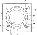
Figure 12 is the cut-open view that capacitance-type pressure sensor of the prior art is shown.Figure 13 is the sectional view along Figure 12 D-D ' line.Figure 14 is the sectional view along Figure 12 E-E ' line.
As shown in figure 12, by the first or second Sapphire Substrate 202A and 202B Direct Bonding are formed sensor main body 202.In sensor main body 202, fixed electorde 201 and movable electrode 203 are be arranged in parallel to face with each other.This structure constitutes static capacity type sensor.
The first substrate 202A is thicker than the second substrate 202B.On thickness direction, form three electrodes that pass the first substrate 202A and stretch out hole 204 and an air pressure entrance hole 205.These holes 204 form the extraneous cavity 207 that links to each other with 205 in sensor main body 202.
The second substrate 202B is by the thick outer peripheral portion 10 and the first substrate 202A Direct Bonding.First and second substrates are used by same material and are made, and do not press from both sides any interlayer on its bonding face, so almost there is not the unrelieved stress of bonding.Adopt the first and second substrate 202A and 202B can not cause any diaphragm 209 that causes to change, stable sensor characteristic can be provided because of the time.
On the first substrate 202A, form three electrodes and stretch out hole 204, corresponding respectively with fixed electorde 201, detecting electrode 203A, reference electrode 203B respectively hole 204a, 204b, 204c promptly shown in Figure 14.Hole 204a forms on the position that is passed in the electrode extension 214 that forms on the fixed electorde 201.Electrode stretches out hole 204b, 204c and also is respectively formed at on the corresponding position of the electrode extension 215A that forms on detecting electrode 203A and the reference electrode 203B and 215B.
Electrode is described below stretches out situation.Figure 15 is the amplification view along Figure 13 line F-F '; Figure 16 is the amplification view along Figure 13 line G-G '.
After on the first substrate 202A is bonded directly to as the wafer of the backing material of the second substrate 202B, wafer is divided into a plurality of chips with microtomy.A plurality of connected nails 211 that its lower end is scribbled scolder part (or electrocondution slurry) 212 embed the electrode that (usefulness is pressed in practice) be used for movable electrode 203 according to this and stretch out hole 204b and 204c, and its electrode extension 215A and 215B with detecting electrode 203A and reference electrode 203B is contacted respectively.This structure of heating temporarily melts scolder part 212 under this state, makes its cooled and solidified then.Like this detecting electrode 203A and reference electrode 203B are electrically connected with connected nail 211, as shown in figure 15.
And as shown in figure 16, connected nail 211 pressurization that the lower end is scribbled electrocondution slurry 213 (or scolder part) embeds the electrode that is used for fixing electrode 201 and stretches out hole 204a.Fixed electorde 201 and connected nail 211 are electrically connected by electrocondution slurry 213.
As mentioned above, in traditional capacitance-type pressure sensor, with scolder part 212 or electrocondution slurry 213 electrode 201 203 or connected nail 211 mechanically, electrically couple together.There is following problems like this.
More specifically, when scolder part 212 being used as bonding agent, if can not obtain enough bond strengths to movable electrode 203 wellabilities are low with movable electrode 203 and connected nail 211 electrical connections.If the wellability height, scolder part 212 flows into from electrode extension 215A or 215B, makes movable electrode 203 and fixed electorde 201 short circuits.
When electrocondution slurry 213 during as bonding agent, if the amount of electrocondution slurry 213 is very few, then with scolder part 212 similarly, bond strength descends and bad connection can occur.If the amount of electrocondution slurry 213 is too much, and electrocondution slurry 213 contacts with fixed electorde 201 and makes fixed electorde 201 and movable electrode 203 short circuits.
On the other hand, as shown in figure 16, when fixed electorde 201 was connected with connected nail 211, fixed electorde 201 was not formed on the interface of connected nail 211.In other words, fixed electorde 201 forms and is formed with thereon on the inside surface of sensor element 202 that electrode stretches out hole 204a.Therefore, scolder partly is difficult to realize being electrically connected with fixed electorde 201.
The present invention can overcome above-mentioned traditional shortcoming, and is purpose to be implemented in the sensor that has high bond strength between electrode and link such as the connected nail.
Another object of the present invention is to provide a kind of sensor of being short-circuited between the electrode of preventing.
Another purpose of the present invention is to provide a kind of reliable sensor that is electrically connected of realizing between electrode and link.
A further object of the present invention be to provide a kind of when producing in batches the good sensor of throughput rate high-performance.
To achieve these goals, according to sensor of the present invention, it is characterized in that comprising: sensor main body (2), wherein be formed with a cavity (7), this cavity stretches out hole (4a, 4b, 4c, 31,104a, 104b, 104c, 131) by a plurality of electrodes and links to each other with the outside; The pair of electrodes that in this cavity, is provided with (1,3) in opposed facing mode; A plurality of links (11,12,131), these links stretch out the hole by electrode and embed in the cavity, and are electrically connected with corresponding electrode; And the pad made from conductive material (24,25), these pads be formed in the cavity in the face of electrode stretch out on the position in hole and with corresponding link bonding mutually.Wherein said each link is higher than wellability to electrode surface to the wellability of bond pad surface.Because link is to the wellability height of bond pad surface, the link of partial melting spreads on the whole bond pad surface, makes between pad and the link bonding securely.Thereby can realize the reliable electrical connection between link and the electrode.On the contrary, link is low to the wellability of electrode surface, even the link of partial melting density current from the pad also almost can not flow along electrode surface.Thus, link can not contact pair of electrodes, can not make their short circuits.
A kind of structure as sensor, described pad (24), form being positioned to stretch out on the surface of described electrode (3,3A, 3B, 15A, 15B) of the position of facing mutually in hole (4a, 4b, 4c, 31), and this electrode is connected with corresponding described link (11,12) by described pad with electrode.Thus, electrode can pass link along the direction opposite with electrode direction and stretches out.
In this case,, comprise from electrode and stretch out the connected nail (11) that the hole embeds, and be used for described connected nail is bonded to bonding agent (12) on the described pad as a kind of structure of described link.Because by connected nail and pad bonding being formed link, can realize that link is electrically connected with the reliable of electrode with bonding agent.
In this sensor arrangement, if described bonding agent is made by Sn-Ag, then described electrode surface is made by Pt, and described bond pad surface is made by Au.This is owing to the wellability height of Sn-Ag to Au, and low to the wellability of Pt.
In the another kind structure of sensor, described pad (25), in each inside surface (21a, 21b) of the described sensor main body that constitutes described cavity with electrode stretch out on the hole facing surfaces (21b), stretch out on the position of facing mutually in the hole with electrode and to form, and stretch out the described electrode (1) that forms on the hole at electrode and contact with link (11,12) accordingly.In this structure, electrode can pass link along the direction identical with electrode direction and stretch out.
In this case,, comprise from electrode and stretch out the connected nail (11) that the hole embeds as a kind of structure of link, and be used for described connected nail and described pad be formed on electrode that electrode stretches out the hole side bonding agent of bonding (12) mutually.Also promptly, form the link that connected nail and pad bonding got up by bonding agent.Owing to be provided with the high pad of para-linkage agent wellability in relative position, bonding agent can arrive electrode surface by connected nail, to realize the reliable electrical connection of electrode and connected nail.Reduced bad connection thus.
In this sensor arrangement, if described bonding agent is made by Sn-Ag, then described electrode surface is made by Pt, and described bond pad surface is made by Au.
Another example of link is in the sensor, and the scolder that is stretched out hole (104a, 104b, 104c, 131) by space on the pad in the cavity filling and electrode constitutes.Because electrode stretches out the scolder filling that the hole is used as link, can easily form link.
In this sensor arrangement, if described scolder is made by Sn-Ag, then described electrode surface is made by Pt, and described bond pad surface is made by Au.
In this case, electrode stretches out the hole can be processed to tapered shape, and promptly the outside surface from described sensor main body reduces gradually to its internal diameter of inside surface.This shape that attenuates can make the scolder of fusing flow smoothly.
In addition, in this case, can be at least on stretching out the part of inside surface in hole, electrode be coated with the material high to solder wettability.Can make the scolder of fusing easily flow through electrode thus and stretch out the hole.
The method of making sensor of the present invention, it is characterized in that comprising the following steps: to prepare such parts, wherein, on sensor main body (2), be formed with by a plurality of electrodes and stretch out the cavity (7) that hole (104a, 104b, 104c, 131) links to each other with the external world, in this cavity, be provided with pair of electrodes (1,3) in opposed facing mode, be formed with a plurality ofly by the pads (24,25) that the high conductive material of the wellability of scolder (111) comparison electrode is constituted at this cavity, and these pads are formed on electrode and stretch out on the position of facing mutually in the hole; Stretch out the hole from electrode and inject the scolder of fusing, stretch out the hole to fill up in the cavity space more than the pad and electrode with it to cavity; And the solder cools that makes fusing, electrode is drawn from cavity by being filled in the scolder that electrode stretches out in the hole.Thus, can fill the scolder that electrode stretches out the hole and form sensor as link.
Solder bump (111A) with pre-sizing can also be placed each electrode on the sensor main body outside surface stretch out on the inlet in hole, heat fused, and make flow of solder material.
Can also fix anchor clamps (127) around the inlet that electrode stretches out the hole, place solder bump then.Thus, solder bump can place on the desired position reliably.
The pressure that can also improve the sensor main body outside makes its pressure that is higher than cavity inside, heats then and makes solder fusing.Thus, the scolder of fusing can be forced to flow on the pad.
In this manufacture method, described pad (24) is stretching out when forming on the surface of the locational electrode of facing in the hole (3A, 3B, 15A, 15B) with described electrode, makes described scolder and described pad bonding mutually.Thus, stretch out can passing the link that constitutes by the material material with electrode that electrode stretches out the opposite side in hole.
On the contrary, described pad (25), in each inside surface (21a, 21b) of the described sensor main body that constitutes described cavity with electrode stretch out on the hole facing surfaces (21b), stretch out when forming on the position of facing mutually in the hole with electrode, make described scolder and be formed on the described electrode (1) that described electrode stretches out the hole side and contact.Thus, stretch out can passing the link that constitutes by the material material with electrode that electrode stretches out the opposite side in hole.
In addition, in this manufacture method, stretch out the hole by form described electrode with laser processing method, can make electrode stretch out the hole becomes tapered shape.
Fig. 1 is the cut-open view according to the sensor of first embodiment of the invention;
Fig. 2 is the cut-open view along Fig. 1 center line II-II ';
Fig. 3 is the cut-open view along Fig. 1 center line III-III ';
Fig. 4 is the amplification view along Fig. 2 center line IV-IV ';
Fig. 5 is the amplification view along Fig. 2 center line V-V ';
Fig. 6 (a)~(d) is the cut-open view that each key step of making sensor is shown respectively;
Fig. 7 (a)~(e) is the cut-open view that Fig. 6 each step afterwards is shown respectively;
Fig. 8 is the cut-open view according to the sensor of second embodiment of the invention;
Fig. 9 is the amplification view of IX part among Fig. 8;
Figure 10 is the amplification view of A part among Fig. 8;
Figure 11 (a)~(c) illustrates the cut-open view of each key step of making sensor respectively;
Figure 12 is the cut-open view of conventional pressure sensor.
Figure 13 is the cut-open view along Figure 12 center line D-D ';
Figure 14 is the cut-open view along Figure 12 center line E-E ';
Figure 15 is the amplification view along Figure 13 center line F-F ';
Figure 16 is the amplification view along Figure 13 center line G-G ';
Describe the preferred embodiments of the invention below in detail.(first embodiment)
Fig. 1 is the cut-open view according to the sensor of first embodiment of the invention; Fig. 2 is the cut-open view along Fig. 1 center line II-II '; Fig. 3 is the cut-open view along Fig. 1 center line III-III '; Fig. 4 is the amplification view along Fig. 2 center line IV-IV '; Fig. 5 is the amplification view along Fig. 2 center line V-V '; Fig. 1 is applicable capacitance-type pressure sensor of the present invention.
The space of groove 8 definition that cavity 7 forms by the first substrate 2A with in the central authorities of the second substrate 2B inside surface constitutes.The middle body of the second substrate 2B is because of groove 8 attenuation becoming diaphragm 9.Form pair of stationary electrodes 1 and movable electrode 3 (3A and 3B) on inside surface 21a and 21b respectively, this inside surface 21a and 21b cavity 7 close to each other and between the first and second substrate 2A and 2B faces with each other.
Each pad 24 is made of Au/ restraining barrier/bonding reinforced film.With the bonding reinforced film of electrode in the same manner, this bonding reinforced film also is made of Ti, V, Cr, Nb, Zr, Hf, Ta etc.In the first embodiment, pad 24 is made of Au/Pt/Nb.In the case, as shown in Figure 4, pad 24 has Au upper strata, Pt middle level and Nb lower floor.
When connecting connected nail 11, each connected nail 11 pressurization intercalation electrodes that its lower end scribbled Sn-Ag scolder part 12 stretch out hole 4b~4c, and Sn-Ag scolder part 12 is contacted with pad 24.This structure is heated to the predetermined temperature that makes 12 fusings of Sn-Ag scolder part.Cool off this Sn-Ag scolder part 12 so that connected nail 11 is fixed on the pad 24.Then, by pad 24 and Sn-Ag scolder part 12 detecting electrode 3A and reference electrode 3B are electrically connected with connected nail 11.
When being connected on the connected nail 11, on electrode extension 15A and 15B, form the pad 24 that respectively has the Au surface to movable electrode 3 (3A and 3B).Connected nail 11 by Sn-Ag scolder part 12 and pad 24 mechanically, electrically be connected.Because the wellability of 12 pairs of pads 24 of Sn-Ag scolder part of fusing is very high, bond strength that can be enough connects connected nail 11.In other words, Sn-Ag scolder part 12 flows on the surface of electrode extension 15A and 15B hardly.Thus, Sn-Ag scolder part 12 does not contact fixed electorde 1, thereby can not make movable electrode 3 and fixed electorde 1 short circuit.
As shown in Figure 5, on the second substrate 2B inside surface 21b and electrode extension 14 corresponding positions first electrode 1, form fixed electorde and stretch out conductive welding disk 25.Pad 25 usefulness are made with movable electrode pad 24 identical materials.Pad 25 is connected with fixed electorde connected nail 11 by Sn-Ag scolder part (or electrocondution slurry) 12 and forms link.Sn-Ag scolder part 12 contacts with the electrode extension 14 of fixed electorde 1 to realize being electrically connected of fixed electorde 1 and connected nail 11, has finished capacitance-type pressure sensor thus.
With being connected in the same manner between movable electrode 3 and the connected nail 11, also be connected with Au/Pt/Nd pad 25 between fixed electorde 1 and the connected nail 11 with Sn-Ag scolder part 12, because the wellability height of 12 pairs of pads 25 of Sn-Ag scolder part of fusing can be connected with satisfied bond strength with connected nail 11.Sn-Ag scolder part 12 drawout on the whole surface of pad 25 comes.In having the pressure transducer 20 of dark d for the cavity 7 of number μ m, Sn-Ag scolder part 12 is sprawled on pad 25, by capillarity cavity filling 7, thereby contacts with the electrode extension 14 of fixed electorde 1.Can realize the electrical connection between fixed electorde and the connected nail 11 thus.Because the wellability of 12 pairs of electrode materials of Sn-Ag scolder part is low, Sn-Ag scolder part 12 does not contact with movable electrode 3, can not cause the short circuit of fixed electorde 1 and movable electrode 3.
As mentioned above, as the method that forms link, can stretch out hole 4 to the connected nail 11 pressurization intercalation electrodes that its lower end scribbles Sn-Ag scolder part 12.Yet the present invention is not limited thereto, also can when the wafer state before the second substrate 2B is in section soldered ball or the desired electrode of welding column embedding be stretched out in the hole, embeds connected nail then, heats this structure.This method also can obtain the effect same with said method, and can once form and have the capacitance-type pressure sensor that a plurality of electrodes stretch out structure.
Manufacture method according to the pressure transducer of first embodiment of the invention is described below.Fig. 6 and Fig. 7 illustrate the sectional view of the key step of making pressure transducer respectively.Notice that Fig. 6 and Fig. 7 illustrate the key step of making pressure transducer, this pressure transducer forms successively on an one substrate that cavity, electrode stretch out hole and fixed electorde and another substrate is used as diaphragm.
When making pressure transducer, prepare a thick sapphire wafer 30 (Fig. 6 (a)).Electrode stretches out hole 31 and air pressure entrance hole (not shown) passes sapphire wafer 30 and forms (Fig. 6 (b)).Form electrode with machine work, Laser Processing, ultrasonic machining and so on and stretch out hole 31 and air pressure entrance hole.
The groove 8 that forms desirable thickness on the inside surface of sapphire wafer 30 is as cavity 7 (Fig. 6 (c)).For saphire substrate material, form groove 8 with dry ecthing method, and, then adopt dry ecthing method or wet etch method for glass and alumina substrate material.The flat shape of cavity 7 can be circular, as shown in Figure 2, also can be quadrilateral.
On the desired position of the lower surface of groove 8, form fixed electorde 1 (Fig. 6 (d)).This fixed electorde 1 is made of Pt/ bonding reinforced film.This bonding reinforced film is made of Ti, V, Cr, Nb, Zr, Hf, Ta etc., and with formation such as vacuum evaporation, ion plating, sputters.For bonding film being formed the shape of electrode, form this film with mask or photoresist and etching.
Preparation diaphragm wafer 35 (Fig. 7 (a)).With the mode same, on the position of the expectation on diaphragm wafer 35 inside surfaces, form movable electrode 3 (Fig. 7 (b)) with said fixing electrode 1.
Then, form electrode and stretch out pad 24 and 25 (Fig. 7 (c)).Each pad is made of Au/ restraining barrier/bonding reinforced film such as Au/Pt/Nb film. Form pad 24 or 25 with vacuum evaporation, ion plating, sputter etc.
At last, the connected nail 11 pressurization intercalation electrodes that the lower end scribbled Sn-Ag scolder part 12 stretch out hole 31,240~300 ℃ of heating and fusings down, cool off then connected nail 11 is fixed to (Fig. 7 (e)) on pad 24 and 25.In this way, fixed electorde 1, connected nail 11 and pad 25, movable electrode 3, pad 24 and connected nail 11 mechanically electrically couple together.
Wafer is become after the chip by section, carry out the step of bonding connected nail 11.Alternatively, before section, can embed Sn-Ag scolder part 12 to contact so that they are stretched out once with electrode.According to this method, the column Sn-Ag scolder intercalation electrode of pre-form is stretched out hole 31, and 240~300 ℃ of heating so that with wafer form taking-up electrode.Thus, can realize depending on the batch process of packing method.(second embodiment)
Fig. 8 is the cut-open view according to the sensor of second embodiment of the invention; Fig. 9 is the amplification view of IX part among Fig. 8; Figure 10 is the amplification view of A part among Fig. 8; With Fig. 1 in the same manner, Fig. 8 also is applicable capacitance-type pressure sensor of the present invention.Notice that the label identical with Fig. 1~5 represented same parts, and omits its explanation.
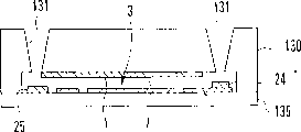
The difference of the pressure transducer 20 among the pressure transducer 120 among Fig. 8 and Fig. 1 is, the structure of link that is used for fixed electorde in the cavity 71 and movable electrode 3 are guided to sensor main body 2 outsides is different.That is, be used for the electrode that cavity 7 links to each other with the outside is stretched out scolder part 111 fillings that hole 104a~104c is used as link.
On the electrode extension 15A of detecting electrode 3A and reference electrode 3B and 15B, form movable electrode respectively and stretch out pad 24.Each pad 24 is same as shown in Figure 4, and is made of for example Au/Pt/Nb.Also be used as the scolder part 111 of bonding agent by constituting with scolder part 12 identical materials Sn-Ag.
The scolder part 111 of the fusing by making q.s flows into electrodes and stretches out hole 104b and 104c, and cooling scolder part 111, is formed for the link of movable electrode 3.At this moment, pad 24 wellabilities that have the Au surface owing to 111 pairs of scolder parts that melt are very high, and scolder part 111 of solidifying and pad 24 be bonding securely.On the other hand, 111 pairs of electrode materials with Pt surface of Sn-Ag scolder part of fusing are low.Even the Sn-Ag scolder part 111 that flows density current from the pad 24 also hardly can be along the surface flow of electrode extension 15A and 15B, and can not make fixed electorde 1 and movable electrode 3 short circuits.
Fixed electorde stretches out pad 25, with the inside surface 21b of the second substrate 2B on the electrode extension 14 corresponding parts of first electrode 1 form.This pad 25 is by constituting with movable electrode pad 24 identical materials.
Similarly be formed for the link of fixed electorde 1 with the link that is used for movable electrode 3.Between this link and the fixed electorde 1 with Sn-Ag scolder part 111 and pad 25 with Au surface bonding securely.Because cavity 7 has the depth d of several μ m, Sn-Ag scolder part 12 is sprawled on pad 25, by capillarity cavity filling 7, thereby contacts with the electrode extension 14 of fixed electorde 1.Can realize the electrical connection between fixed electorde 1 and the connected nail 11 thus.Because the wellability of 111 pairs of electrode materials of Sn-Ag scolder part is low, can not cause the short circuit of fixed electorde 1 and movable electrode 3.
Electrode stretches out hole 104a~104c and is processed to its internal diameter and diminishes gradually to inside surface from the outside surface of the first substrate 2A.This tapered shape can make the scolder part 111 of fusing gently flow.Notice that do not carry out this processing even electrode stretches out hole 111, the scolder part 111 of fusing also can flow.Therefore, electrode stretches out the hole does not always need to be processed to tapered shape.
The manufacture method of the pressure transducer of the present embodiment is described below.Figure 11 illustrates the sectional view of the key step of making pressure transducer respectively.Notice that Figure 11 illustrates the key step of making pressure transducer, this pressure transducer forms successively on an one substrate that cavity, electrode stretch out hole and fixed electorde and another substrate is used as diaphragm.
At first, the parts of preparation shown in Figure 11 (a), these parts use the mode identical with Fig. 7 (a)~7 (d) with Fig. 6 (a)~6 (d) to make.The internal diameter that each electrode stretches out hole 131 is about 50~500 μ m, is about 300~700 μ m from pad 24 or 25 height that stretch out the outlet (forming the inside surface of first substrate 130 of cavity 7) in hole 131 to electrode.For a part of electrode being stretched out on the hole 131 is cut carefully, shown in Figure 11 (a), available laser processing method forms the electrode that passes first substrate 130 and stretches out hole 131.
(part on the outside surface of first substrate 130) is provided with Sn-Ag soldered ball 111A in electrode stretches out the inlet in hole 131.As the size of the soldered ball 111A of solder bump, but with in next step with the pad 24 in scolder part 111 cavity fillings 7 of fusing or 25 above spaces and and electrode stretch out hole 131 and be as the criterion.The diameter of soldered ball 111A stretches out the internal diameter of the inlet in hole 131 greater than electrode, and soldered ball 111A just can not fall into cavity 7 like this.If stretch out the inlet in hole 131 along electrode anchor clamps 127 are set, just can easily soldered ball 111A be placed desired position (Figure 11 (b)).
Then,, make it stretch out hole 131 and flow on the pad 24,25 with fusing soldered ball 111A 240~300 ℃ of heating sensor main bodys by electrode.Then, cooling will be stretched out in the hole 131 with scolder part 111 embedded electrodes of pad 24,25 bondings, and this scolder part 111 is as link.Remove anchor clamps 127 at last, finish pressure transducer (Figure 11 (c)).
Under above-mentioned condition (internal diameter of connected nail 131, from pad 24 or 25 height and temperature), because of its scolder part 111 from remelting arrives pads 24,25 from connected nail 131 to the outlet of connected nail 131.But, depend on that the internal diameter of connected nail 131, the one-tenth of scolder part 111 grade, the scolder part of fusing 111 since surface pressing of scolder part 111, friction factor of connected nail 131 inside surfaces and so on may not can flow into cavity 7 because of gravity.In this case, can impel the scolder part 111 of fusing inwardly to flow with following method.
The first, utilize the difference between the interior pressure of the external pressure of sensor main body 2 and cavity 7.In the step shown in Figure 11 (b), cover each electrode with soldered ball 111A and stretch out hole 131.If have air pressure entrance hole (referring to the air pressure entrance hole 5 among Fig. 3), cover this hole with sealed cavity 7.This structure of heating under this state, the external pressure of sensor main body 2 is set to enough height simultaneously.Then, the scolder part 111 of fusing can be stretched out at electrode and be stretched out hole 131 from electrode by force under the pressure differential effect of 131 both sides, hole and import cavitys 7.In addition, when the air pressure entrance hole is arranged, cavity 7 inner pumpings are pressed to reduce in the cavity 7, also can obtain same effect with this hole.
The second, increase the wellability that electrode stretches out hole 131 inside surfaces.For example, increase the wellability of the scolder part 111 of fusing by the inside surface that stretches out hole 131 with Au film coated electrode.Thus, the scolder part 111 of fusing can easily flow.By only cover the part of stretching out hole 131 inlets around electrode with the Au film, also can obtain same effect.
In the above-described embodiment, the present invention is used on the capacitance-type pressure sensor.But the present invention is not limited thereto, also can be used on any sensor such as the capacitance acceleration transducer, outside as long as the electrode that forms in the cavity of sensor main body stretches out.
Cavity forms by form groove on one of two substrates.But, also can form cavity by between two substrates, embedding partition.
As mentioned above, in sensor of the present invention, use to the infiltrating link of electrode with to the high pad of electrode wellability electrode is drawn.Thus can be link and the firm bonding of electrode.Simultaneously, can be electrically connected electrode and link reliably, and can not make the link of fusing partly flow on the electrode surface or make electric pole short circuit, therefore, can obtain at the sensor that is better than traditional sensors aspect output and the mass productivity greatly.
In the case, connected nail and pad bonding are got up to form link can realize more reliable electrical connection between link and the electrode by having used.
Stretch out the hole and scolder can easily be formed link as link by fill electrode with scolder.
At this moment, be processed into tapered shape if electrode stretches out the hole, the scolder of fusing can gently flow.
Be coated with the material high if electrode stretches out the inside surface in hole, can form reliably on the link that constitutes by embedding scolder solder wettability.
According to sensor manufacture method of the present invention, the scolder of fusing can stretch out orifice flow to pad from electrode.Fill electrode with the scolder of fusing and stretch out the hole, cool off, and scolder is embedded in wherein.As link, can promote the formation of link with this scolder.
In this manufacture method, stretch out the hole if form electrode with Laser Processing, can stretch out electrode that tapered shape is processed in the hole so that the scolder of fusing flows reposefully.
Claims (18)
1. sensor is characterized in that comprising:
Sensor main body wherein is formed with a cavity, and this cavity stretches out the hole by a plurality of electrodes and links to each other with the outside;
The pair of electrodes that in this cavity, is provided with in opposed facing mode;
A plurality of bonding agents, these bonding agents stretch out the hole by electrode and embed in the cavity, and are electrically connected with corresponding electrode; And
With the pad that conductive material is made, these pads be formed in the cavity stretch out on the position of facing in the hole with electrode and with corresponding bonding agent bonding mutually.
Wherein said each bonding agent is higher than wellability to electrode surface to the wellability of bond pad surface.
2. sensor as claimed in claim 1 is characterized in that:
Described pad forms being positioned to stretch out on the surface of described electrode of the position of facing mutually in the hole with electrode, and
Described electrode is connected with corresponding described bonding agent by described pad.
3. sensor as claimed in claim 2 is characterized in that:
Also comprise from electrode and stretch out the connected nail that the hole embeds, described connected nail is bonded on the described pad by described bonding agent.
4. sensor as claimed in claim 3 is characterized in that:
Described bonding agent is made by Sn-Ag, and described electrode surface is made by Pt, and described bond pad surface is made by Au.
5. sensor as claimed in claim 1 is characterized in that:
Described pad, in each inside surface of the described sensor main body that constitutes described cavity with electrode stretch out on the facing surfaces of hole, stretch out on the position of facing in the hole with electrode and to form, and
The described electrode that stretches out hole side formation at electrode contacts with corresponding bonding agent.
6. sensor as claimed in claim 5 is characterized in that:
Also comprise from electrode and stretch out the connected nail that the hole embeds, described connected nail is bonded on the described pad by described bonding agent.
7. sensor as claimed in claim 6 is characterized in that:
Described bonding agent is made by Sn-Ag, and described electrode surface is made by Pt, and described bond pad surface is made by Au.
8. sensor as claimed in claim 1 is characterized in that:
Described bonding agent is made up of the scolder that space more than the pad and electrode described in the cavity filling stretch out the hole.
9. sensor as claimed in claim 8 is characterized in that:
Described bonding agent is made by Sn-Ag, and described electrode surface is made by Pt, and described bond pad surface is made by Au.
10. sensor as claimed in claim 8 is characterized in that:
Electrode stretches out the hole and is processed to tapered shape, and promptly the outside surface from described sensor main body reduces gradually to its diameter of inside surface.
11. sensor as claimed in claim 8 is characterized in that:
At least on stretching out the part of inside surface in hole, electrode is coated with the material high to solder wettability.
12. a method of making sensor is characterized in that comprising the following steps:
Prepare such parts, wherein, on sensor main body, be formed with by a plurality of electrodes and stretch out hole and the extraneous cavity that is connected, in this cavity, be provided with pair of electrodes in opposed facing mode, be formed with a plurality ofly by the pads that the high conductive material of the wellability of scolder comparison electrode is constituted at this cavity, and these pads are formed on electrode and stretch out on the position of facing mutually in the hole;
Stretch out the hole from electrode and inject the scolder of fusing, to stretch out the hole with space more than the pad and electrode in its cavity filling to cavity; And
Make melting solder cooling, electrode is drawn from cavity by being filled in the scolder that electrode stretches out in the hole.
13. the method for making sensor as claimed in claim 12 is characterized in that:
Comprise that also the solder bump that will have pre-sizing places each electrode that is positioned on the sensor main body outside surface to stretch out on the inlet in hole, heat fused, and make flow of solder material.
14. the method for making sensor as claimed in claim 13 is characterized in that:
Comprise that also the inlet that stretches out the hole around electrode fixes anchor clamps, place solder bump then.
15. the method for making sensor as claimed in claim 13 is characterized in that:
Also comprise the pressure that improves the sensor main body outside, make its pressure that is higher than cavity inside, heat then and make solder fusing.
16. the method for making sensor as claimed in claim 12 is characterized in that:
Described pad forms stretching out on the surface of the locational electrode of facing in the hole with described electrode, and makes described scolder and described pad bonding mutually.
17. the method for making sensor as claimed in claim 12 is characterized in that:
Described pad, in each inside surface of the described sensor main body that constitutes described cavity with electrode stretch out on the facing surfaces of hole, this pad is stretched out in the face of electrode on the position in hole form, and
Make described scolder and be formed on the described electrode that described electrode stretches out the hole side and contact.
18. the method for making sensor as claimed in claim 12 is characterized in that:
Form described electrode with laser processing method and stretch out the hole.
Applications Claiming Priority (2)
| Application Number | Priority Date | Filing Date | Title |
|---|---|---|---|
| JP61111/1998 | 1998-03-12 | ||
| JP6111198 | 1998-03-12 |
Publications (2)
| Publication Number | Publication Date |
|---|---|
| CN1258350A CN1258350A (en) | 2000-06-28 |
| CN1138136C true CN1138136C (en) | 2004-02-11 |
Family
ID=13161655
Family Applications (1)
| Application Number | Title | Priority Date | Filing Date |
|---|---|---|---|
| CNB998002682A Expired - Fee Related CN1138136C (en) | 1998-03-12 | 1999-03-11 | Sensor and method of producing same |
Country Status (7)
| Country | Link |
|---|---|
| US (1) | US6382030B1 (en) |
| EP (1) | EP0982576B1 (en) |
| JP (1) | JP3447062B2 (en) |
| KR (1) | KR100329026B1 (en) |
| CN (1) | CN1138136C (en) |
| DE (1) | DE69942382D1 (en) |
| WO (1) | WO1999046570A1 (en) |
Families Citing this family (33)
| Publication number | Priority date | Publication date | Assignee | Title |
|---|---|---|---|---|
| JP3588286B2 (en) | 1999-10-06 | 2004-11-10 | 株式会社山武 | Capacitive pressure sensor |
| JP3877484B2 (en) * | 2000-02-29 | 2007-02-07 | アルプス電気株式会社 | Input device |
| JP3771425B2 (en) | 2000-07-04 | 2006-04-26 | 株式会社山武 | Capacitive pressure sensor and manufacturing method thereof |
| DE10052053A1 (en) * | 2000-10-19 | 2002-04-25 | Endress Hauser Gmbh Co | Pressure measurement cell has contact pin fed through base body to electrode for capacitance measurement; contact pin, jointing solder and membrane bed form smooth surface |
| JP2002350266A (en) * | 2001-05-24 | 2002-12-04 | Kyocera Corp | Package for pressure detector |
| US7353719B2 (en) * | 2002-03-28 | 2008-04-08 | Seiko Epson Corporation | Pressure sensor and method for fabricating the same |
| JP4250387B2 (en) * | 2002-08-20 | 2009-04-08 | 長野計器株式会社 | Converter and manufacturing method thereof |
| JP4503963B2 (en) * | 2003-09-18 | 2010-07-14 | 株式会社山武 | Sensor electrode extraction method |
| JP2005172483A (en) * | 2003-12-09 | 2005-06-30 | Toyo Commun Equip Co Ltd | Pressure sensor |
| JP2005201818A (en) * | 2004-01-16 | 2005-07-28 | Alps Electric Co Ltd | Pressure sensor |
| JP2005227089A (en) * | 2004-02-12 | 2005-08-25 | Denso Corp | Dynamics quantity sensor apparatus |
| JP3930862B2 (en) * | 2004-02-13 | 2007-06-13 | 東京エレクトロン株式会社 | Capacitive sensor |
| DE102004018408A1 (en) * | 2004-04-16 | 2005-11-03 | Robert Bosch Gmbh | Capacitive pressure sensor and method of manufacture |
| US7089798B2 (en) * | 2004-10-18 | 2006-08-15 | Silverbrook Research Pty Ltd | Pressure sensor with thin membrane |
| JP2006260971A (en) * | 2005-03-17 | 2006-09-28 | Alps Electric Co Ltd | Input device |
| US9243756B2 (en) | 2006-04-20 | 2016-01-26 | Delta Faucet Company | Capacitive user interface for a faucet and method of forming |
| US8162236B2 (en) | 2006-04-20 | 2012-04-24 | Masco Corporation Of Indiana | Electronic user interface for electronic mixing of water for residential faucets |
| JP2008039593A (en) * | 2006-08-07 | 2008-02-21 | Alps Electric Co Ltd | Capacitance type acceleration sensor |
| JP5305644B2 (en) * | 2006-12-25 | 2013-10-02 | 京セラ株式会社 | PACKAGE FOR PRESSURE SENSOR, MANUFACTURING METHOD THEREOF, AND PRESSURE SENSOR |
| CN101809691B (en) * | 2007-04-20 | 2012-07-18 | 英克-罗吉克斯有限公司 | In-molded capacitive switch |
| US8198979B2 (en) | 2007-04-20 | 2012-06-12 | Ink-Logix, Llc | In-molded resistive and shielding elements |
| JP4984068B2 (en) * | 2007-10-04 | 2012-07-25 | セイコーエプソン株式会社 | Pressure sensor |
| JP2010008115A (en) * | 2008-06-25 | 2010-01-14 | Kyocera Corp | Base for pressure detection apparatus and pressure-detecting apparatus |
| KR101044914B1 (en) * | 2009-10-30 | 2011-06-28 | (주) 유니크코리아엔아이 | Capacitive pressure sensor with diffusion barrier |
| US9074357B2 (en) | 2011-04-25 | 2015-07-07 | Delta Faucet Company | Mounting bracket for electronic kitchen faucet |
| US9057184B2 (en) | 2011-10-19 | 2015-06-16 | Delta Faucet Company | Insulator base for electronic faucet |
| TWI518804B (en) * | 2012-02-14 | 2016-01-21 | Asia Pacific Microsystems Inc | Monolithic compound sensor and its package |
| US9333698B2 (en) | 2013-03-15 | 2016-05-10 | Delta Faucet Company | Faucet base ring |
| US9464950B2 (en) * | 2013-11-15 | 2016-10-11 | Rosemount Aerospace Inc. | Capacitive pressure sensors for high temperature applications |
| US9621975B2 (en) * | 2014-12-03 | 2017-04-11 | Invensense, Inc. | Systems and apparatus having top port integrated back cavity micro electro-mechanical system microphones and methods of fabrication of the same |
| JP6500713B2 (en) * | 2015-09-07 | 2019-04-17 | Tdk株式会社 | Acceleration sensor |
| CN105424231B (en) * | 2015-12-23 | 2019-01-08 | 深圳顺络电子股份有限公司 | A kind of high-precision ceramic pressure sensor |
| US10697628B2 (en) | 2017-04-25 | 2020-06-30 | Delta Faucet Company | Faucet illumination device |
Family Cites Families (20)
| Publication number | Priority date | Publication date | Assignee | Title |
|---|---|---|---|---|
| JPS58198739A (en) * | 1982-05-14 | 1983-11-18 | Matsushita Electric Ind Co Ltd | Electrostatic capacity type pressure sensor |
| US4617606A (en) * | 1985-01-31 | 1986-10-14 | Motorola, Inc. | Capacitive pressure transducer |
| US4701826A (en) * | 1986-10-30 | 1987-10-20 | Ford Motor Company | High temperature pressure sensor with low parasitic capacitance |
| JPS63192203A (en) * | 1987-02-04 | 1988-08-09 | 日本鋼管株式会社 | Thin film temperature sensor |
| EP0339981A3 (en) * | 1988-04-29 | 1991-10-09 | Schlumberger Industries, Inc. | Laminated semiconductor sensor with overpressure protection |
| JPH0623782B2 (en) * | 1988-11-15 | 1994-03-30 | 株式会社日立製作所 | Capacitance type acceleration sensor and semiconductor pressure sensor |
| JP2772111B2 (en) * | 1990-04-27 | 1998-07-02 | 豊田工機株式会社 | Capacitive pressure sensor |
| JPH05264576A (en) * | 1992-03-19 | 1993-10-12 | Hitachi Ltd | Acceleration sensor |
| JP2533272B2 (en) * | 1992-11-17 | 1996-09-11 | 住友電気工業株式会社 | Method for manufacturing semiconductor device |
| JPH06160420A (en) * | 1992-11-19 | 1994-06-07 | Omron Corp | Semiconductor acceleration sensor and its manufacture |
| JP2852593B2 (en) * | 1993-03-11 | 1999-02-03 | 株式会社山武 | Capacitive pressure sensor |
| US5503285A (en) * | 1993-07-26 | 1996-04-02 | Litton Systems, Inc. | Method for forming an electrostatically force balanced silicon accelerometer |
| JPH07113817A (en) * | 1993-10-15 | 1995-05-02 | Hitachi Ltd | Acceleration sensor |
| JPH07307410A (en) * | 1994-05-16 | 1995-11-21 | Hitachi Ltd | Semiconductor device |
| JP3348528B2 (en) * | 1994-07-20 | 2002-11-20 | 富士通株式会社 | Method for manufacturing semiconductor device, method for manufacturing semiconductor device and electronic circuit device, and electronic circuit device |
| US5528452A (en) * | 1994-11-22 | 1996-06-18 | Case Western Reserve University | Capacitive absolute pressure sensor |
| JPH08254474A (en) * | 1995-03-15 | 1996-10-01 | Omron Corp | Semiconductor sensor |
| JP3369410B2 (en) * | 1996-09-02 | 2003-01-20 | 松下電器産業株式会社 | Mounting method of semiconductor device |
| EP0862051A4 (en) * | 1996-09-19 | 1999-12-08 | Hokuriku Elect Ind | Electrostatic capacity type pressure sensor |
| JP3576727B2 (en) * | 1996-12-10 | 2004-10-13 | 株式会社デンソー | Surface mount type package |
-
1999
- 1999-03-11 WO PCT/JP1999/001190 patent/WO1999046570A1/en active IP Right Grant
- 1999-03-11 CN CNB998002682A patent/CN1138136C/en not_active Expired - Fee Related
- 1999-03-11 JP JP54563199A patent/JP3447062B2/en not_active Expired - Fee Related
- 1999-03-11 KR KR1019997010405A patent/KR100329026B1/en not_active IP Right Cessation
- 1999-03-11 DE DE69942382T patent/DE69942382D1/en not_active Expired - Lifetime
- 1999-03-11 US US09/423,933 patent/US6382030B1/en not_active Expired - Lifetime
- 1999-03-11 EP EP99939217A patent/EP0982576B1/en not_active Expired - Lifetime
Also Published As
| Publication number | Publication date |
|---|---|
| JP3447062B2 (en) | 2003-09-16 |
| CN1258350A (en) | 2000-06-28 |
| KR100329026B1 (en) | 2002-03-18 |
| WO1999046570A1 (en) | 1999-09-16 |
| US6382030B1 (en) | 2002-05-07 |
| KR20010012451A (en) | 2001-02-15 |
| DE69942382D1 (en) | 2010-07-01 |
| EP0982576A1 (en) | 2000-03-01 |
| EP0982576A4 (en) | 2007-07-18 |
| EP0982576B1 (en) | 2010-05-19 |
Similar Documents
| Publication | Publication Date | Title |
|---|---|---|
| CN1138136C (en) | Sensor and method of producing same | |
| US7148576B2 (en) | Semiconductor device and method of fabricating the same | |
| JP5624649B2 (en) | Fusible input / output interconnect system and method for flip chip packaging with stud bumps attached to a substrate | |
| CN1260796C (en) | Side welding method for flip-chip semiconductor device | |
| US7510902B2 (en) | Image sensor chip package and method of fabricating the same | |
| JP4542768B2 (en) | Solid-state imaging device and manufacturing method thereof | |
| KR100735933B1 (en) | Heat-conducting adhesive compound and a method for producing a heat-conducting adhesive compound | |
| CN1519928A (en) | Semiconductor device and its mfg. method | |
| CN1841718A (en) | Semiconductor device and manufacturing method of the same | |
| CN1572718A (en) | Semiconductor device and manufacturing method of the same | |
| CN1649119A (en) | Semiconductor device | |
| US7679188B2 (en) | Semiconductor device having a bump formed over an electrode pad | |
| CN1574263A (en) | Semiconductor package having semiconductor constructing body and method of manufacturing the same | |
| CN1890789A (en) | Process for packaging components, and packaged components | |
| CN1956158A (en) | Manufacturing method and middle structure of solder projection | |
| CN1299518A (en) | Semiconductor pakage and flip-chiop bonding method therefor | |
| JP3729817B2 (en) | Method for manufacturing solid-state imaging device | |
| JP5052459B2 (en) | Semiconductor sensor device | |
| CN1437232A (en) | Chip package structure and its making process | |
| CN1841688A (en) | Method of manufacturing stack-type semiconductor device and method of manufacturing stack-type electronic component | |
| JP2005123559A (en) | Thermal enhanced package structure and its forming method | |
| JP2008288327A (en) | Semiconductor device, and manufacturing method thereof | |
| CN1848413A (en) | Strain silicon wafer with a crystal orientation (100) in flip chip bga package | |
| JP2000114206A (en) | Manufacture of semiconductor package | |
| JP2006245359A (en) | Photoelectric conversion device, and manufacturing method thereof |
Legal Events
| Date | Code | Title | Description |
|---|---|---|---|
| C06 | Publication | ||
| PB01 | Publication | ||
| C10 | Entry into substantive examination | ||
| SE01 | Entry into force of request for substantive examination | ||
| C14 | Grant of patent or utility model | ||
| GR01 | Patent grant | ||
| CF01 | Termination of patent right due to non-payment of annual fee | ||
| CF01 | Termination of patent right due to non-payment of annual fee |
Granted publication date: 20040211 Termination date: 20170311 |