JP3729817B2 - Method for manufacturing solid-state imaging device - Google Patents
Method for manufacturing solid-state imaging device Download PDFInfo
- Publication number
- JP3729817B2 JP3729817B2 JP2003123842A JP2003123842A JP3729817B2 JP 3729817 B2 JP3729817 B2 JP 3729817B2 JP 2003123842 A JP2003123842 A JP 2003123842A JP 2003123842 A JP2003123842 A JP 2003123842A JP 3729817 B2 JP3729817 B2 JP 3729817B2
- Authority
- JP
- Japan
- Prior art keywords
- base
- imaging device
- tape material
- state imaging
- solid
- Prior art date
- Legal status (The legal status is an assumption and is not a legal conclusion. Google has not performed a legal analysis and makes no representation as to the accuracy of the status listed.)
- Expired - Fee Related
Links
- 238000003384 imaging method Methods 0.000 title claims description 66
- 238000004519 manufacturing process Methods 0.000 title claims description 36
- 238000000034 method Methods 0.000 title claims description 29
- 239000000463 material Substances 0.000 claims description 89
- 239000011347 resin Substances 0.000 claims description 56
- 229920005989 resin Polymers 0.000 claims description 56
- 239000002184 metal Substances 0.000 claims description 48
- 229910052751 metal Inorganic materials 0.000 claims description 48
- 238000000465 moulding Methods 0.000 claims description 29
- 238000010438 heat treatment Methods 0.000 claims description 8
- 230000002093 peripheral effect Effects 0.000 claims description 6
- 239000011810 insulating material Substances 0.000 claims description 4
- 238000007789 sealing Methods 0.000 claims description 4
- 238000003825 pressing Methods 0.000 claims description 3
- 230000000694 effects Effects 0.000 description 3
- 238000007747 plating Methods 0.000 description 3
- 229910000679 solder Inorganic materials 0.000 description 3
- 229910045601 alloy Inorganic materials 0.000 description 2
- 239000000956 alloy Substances 0.000 description 2
- 230000003287 optical effect Effects 0.000 description 2
- 229910000881 Cu alloy Inorganic materials 0.000 description 1
- 230000002411 adverse Effects 0.000 description 1
- 238000006243 chemical reaction Methods 0.000 description 1
- 238000005520 cutting process Methods 0.000 description 1
- 238000005516 engineering process Methods 0.000 description 1
- 239000003822 epoxy resin Substances 0.000 description 1
- 239000011521 glass Substances 0.000 description 1
- PCHJSUWPFVWCPO-UHFFFAOYSA-N gold Chemical compound [Au] PCHJSUWPFVWCPO-UHFFFAOYSA-N 0.000 description 1
- 239000010931 gold Substances 0.000 description 1
- 229910052737 gold Inorganic materials 0.000 description 1
- 239000000088 plastic resin Substances 0.000 description 1
- 229920000647 polyepoxide Polymers 0.000 description 1
- 239000000758 substrate Substances 0.000 description 1
Images


Classifications
-
- H—ELECTRICITY
- H01—ELECTRIC ELEMENTS
- H01L—SEMICONDUCTOR DEVICES NOT COVERED BY CLASS H10
- H01L27/00—Devices consisting of a plurality of semiconductor or other solid-state components formed in or on a common substrate
- H01L27/14—Devices consisting of a plurality of semiconductor or other solid-state components formed in or on a common substrate including semiconductor components sensitive to infrared radiation, light, electromagnetic radiation of shorter wavelength or corpuscular radiation and specially adapted either for the conversion of the energy of such radiation into electrical energy or for the control of electrical energy by such radiation
- H01L27/144—Devices controlled by radiation
- H01L27/146—Imager structures
- H01L27/14601—Structural or functional details thereof
-
- H—ELECTRICITY
- H01—ELECTRIC ELEMENTS
- H01L—SEMICONDUCTOR DEVICES NOT COVERED BY CLASS H10
- H01L23/00—Details of semiconductor or other solid state devices
-
- H—ELECTRICITY
- H01—ELECTRIC ELEMENTS
- H01L—SEMICONDUCTOR DEVICES NOT COVERED BY CLASS H10
- H01L2224/00—Indexing scheme for arrangements for connecting or disconnecting semiconductor or solid-state bodies and methods related thereto as covered by H01L24/00
- H01L2224/01—Means for bonding being attached to, or being formed on, the surface to be connected, e.g. chip-to-package, die-attach, "first-level" interconnects; Manufacturing methods related thereto
- H01L2224/02—Bonding areas; Manufacturing methods related thereto
- H01L2224/04—Structure, shape, material or disposition of the bonding areas prior to the connecting process
- H01L2224/05—Structure, shape, material or disposition of the bonding areas prior to the connecting process of an individual bonding area
- H01L2224/0554—External layer
- H01L2224/0556—Disposition
- H01L2224/05568—Disposition the whole external layer protruding from the surface
-
- H—ELECTRICITY
- H01—ELECTRIC ELEMENTS
- H01L—SEMICONDUCTOR DEVICES NOT COVERED BY CLASS H10
- H01L2224/00—Indexing scheme for arrangements for connecting or disconnecting semiconductor or solid-state bodies and methods related thereto as covered by H01L24/00
- H01L2224/01—Means for bonding being attached to, or being formed on, the surface to be connected, e.g. chip-to-package, die-attach, "first-level" interconnects; Manufacturing methods related thereto
- H01L2224/02—Bonding areas; Manufacturing methods related thereto
- H01L2224/04—Structure, shape, material or disposition of the bonding areas prior to the connecting process
- H01L2224/05—Structure, shape, material or disposition of the bonding areas prior to the connecting process of an individual bonding area
- H01L2224/0554—External layer
- H01L2224/05573—Single external layer
-
- H—ELECTRICITY
- H01—ELECTRIC ELEMENTS
- H01L—SEMICONDUCTOR DEVICES NOT COVERED BY CLASS H10
- H01L2224/00—Indexing scheme for arrangements for connecting or disconnecting semiconductor or solid-state bodies and methods related thereto as covered by H01L24/00
- H01L2224/01—Means for bonding being attached to, or being formed on, the surface to be connected, e.g. chip-to-package, die-attach, "first-level" interconnects; Manufacturing methods related thereto
- H01L2224/10—Bump connectors; Manufacturing methods related thereto
- H01L2224/15—Structure, shape, material or disposition of the bump connectors after the connecting process
- H01L2224/16—Structure, shape, material or disposition of the bump connectors after the connecting process of an individual bump connector
- H01L2224/161—Disposition
- H01L2224/16151—Disposition the bump connector connecting between a semiconductor or solid-state body and an item not being a semiconductor or solid-state body, e.g. chip-to-substrate, chip-to-passive
- H01L2224/16221—Disposition the bump connector connecting between a semiconductor or solid-state body and an item not being a semiconductor or solid-state body, e.g. chip-to-substrate, chip-to-passive the body and the item being stacked
- H01L2224/16225—Disposition the bump connector connecting between a semiconductor or solid-state body and an item not being a semiconductor or solid-state body, e.g. chip-to-substrate, chip-to-passive the body and the item being stacked the item being non-metallic, e.g. insulating substrate with or without metallisation
-
- H—ELECTRICITY
- H01—ELECTRIC ELEMENTS
- H01L—SEMICONDUCTOR DEVICES NOT COVERED BY CLASS H10
- H01L2924/00—Indexing scheme for arrangements or methods for connecting or disconnecting semiconductor or solid-state bodies as covered by H01L24/00
- H01L2924/0001—Technical content checked by a classifier
- H01L2924/00014—Technical content checked by a classifier the subject-matter covered by the group, the symbol of which is combined with the symbol of this group, being disclosed without further technical details
Landscapes
- Physics & Mathematics (AREA)
- Engineering & Computer Science (AREA)
- Power Engineering (AREA)
- Condensed Matter Physics & Semiconductors (AREA)
- General Physics & Mathematics (AREA)
- Computer Hardware Design (AREA)
- Microelectronics & Electronic Packaging (AREA)
- Electromagnetism (AREA)
- Solid State Image Pick-Up Elements (AREA)
- Transforming Light Signals Into Electric Signals (AREA)
- Light Receiving Elements (AREA)
Description
【0001】
【発明の属する技術分野】
本発明は、CCD等の撮像素子を基台に搭載して構成される固体撮像装置の製造方法に関する。
【0002】
【従来の技術】
固体撮像装置は、ビデオカメラやスチルカメラ等に広く用いられ、CCD等の撮像素子を絶縁性材料からなる基台に搭載し、受光領域を透光板で覆ったパッケージの形態で提供される。装置の小型化のため、撮像素子は、ベアチップのままで基台に搭載される(例えば、特許文献1を参照)。そのような固体撮像装置の従来例について、図9を参照して説明する。
【0003】
図9における基台31は、平面形状は中央部に開口部32を有する枠状であり、断面形状は全体に一様な厚みを有する板状である。基台31の下面には、開口部32の近傍から外周端面に亘って、金メッキ層からなる配線33が付設されている。基台31における配線33が形成された面に、CCD等から構成された撮像素子4が実装され、その受光領域4aが開口部32に面している。基台31の上面には、開口部32を覆ってガラスからなる透光板5が取り付けられている。撮像素子4の端部の周辺にはシール樹脂6が充填され、撮像素子4の端部と基台31の間の隙間を密封している。以上のように受光領域4aは、開口部32に形成された閉鎖空間内に配置されている。
【0004】
撮像素子4における受光領域4aと同一の面に、受光領域4aの回路と接続された電極パッド(図示せず)が配置され、電極パッド上にバンプ(突起電極)7が設けられている。配線33における開口部32に隣接した端部が内部端子部33aを形成し、バンプ7を介して撮像素子4の電極パッドと接続されている。
【0005】
この固体撮像装置は、図示されたように透光板5側を上方にむけた状態で回路基板上に搭載される。配線33における基台31の外周端部の下面に配置された部分が外部端子部33bを形成し、回路基板上の電極との接続に用いられる。各配線33の外部端子部33b上にはんだボール8が付設され、回路基板上の電極との接続に用いられる。また、はんだボール8は、基台31を回路基板面から適切な高さに維持する機能も有する。
【0006】
透光板5の上部には、撮像光学系が組み込まれた鏡筒(図示せず)が、受光領域4aとの相互の位置関係を所定の精度で設定されて装着される。鏡筒に組み込まれた撮像光学系を通して、被撮像対象からの光が受光領域4aに集光され、光電変換される。
【0007】
【特許文献1】
特開2002−43554号公報
【0008】
【発明が解決しようとする課題】
しかしながら、上記従来例の固体撮像装置の構成では、基台31の十分な平坦度を得ることは困難である。つまり、基台31が開口部32を有する枠状であることにより、樹脂成形を行うと、その断面形状の捩れ、あるいは反りを生じる傾向がある。撮像素子4が搭載される面の平坦度が悪いと、撮像素子4の位置が安定せず、受光領域4aに対して鏡筒を精度良く位置決めすることができない。
【0009】
また、特許文献1においては記載がないが、従来例においては配線33がメッキにより形成されていたため、基台31にメッキを施す工程が煩雑で、形成される配線33の寸法精度にばらつきを生じ易く、また高コストである。
【0010】
本発明は、撮像素子を搭載するための基台を複数個一度に、実用的に十分な平坦度で効率的に形成することが可能な製造方法を提供することを目的とする。また、寸法精度のばらつきが少なく低コストで配線を付設することが可能な固体撮像装置の製造方法を提供することを目的とする。
【0011】
【課題を解決するための手段】
本発明の固体撮像装置の製造方法は、内側領域に開口部が形成された枠状の平面形状を有し厚みが実質的に一様な絶縁性の材料からなる基台と、前記基台の一方の面に前記開口部側から外側に向かって延在するように付設された配線と、前記基台における前記配線の付設面に、受光領域が前記開口部に面するように搭載された撮像素子とを備え、前記配線は前記開口部側に位置する内部端子部と前記基台の外周部に位置する外部端子部とを有し、前記撮像素子の電極と前記内部端子部とが電気的に接続された固体撮像装置を製造する方法である。
【0012】
上記課題を解決するために、本発明の製造方法は、複数個の前記基台を樹脂成形するためのキャビティを形成する一対の金型と、複数個の前記基台に対応する複数組の前記配線を形成するための金属薄板リードを担持するテープ材とを用い、前記金型には、前記基台の厚さ方向の位置決め孔を複数形成するための複数個のピンを設け、前記一対の金型の間に前記テープ材を装填して、前記キャビティにおける前記複数の基台に対応する領域に各々、各組の前記金属薄板リードを配置し、前記キャビティに封止樹脂を充填して硬化させ、前記金属薄板リードが埋め込まれた樹脂成型体を前記金型から取り出し、前記テープ材を前記樹脂成型体から除去し、前記樹脂成型体を前記配線が付設された前記基台に各々対応する複数の個片に分離し、前記基台における前記配線が付設された面に前記撮像素子を実装することを特徴とする。
【0013】
【発明の実施の形態】
本発明の固体撮像装置の製造方法によれば、複数個の基台を樹脂成形するためのキャビティを形成する一対の金型と、複数個の基台に対応する複数組の配線を形成する金属薄板リードを担持するテープ材とを用い、基台の成形工程で金属薄板リードを埋め込むことにより、基台の捩れや反りを生じることが抑制される。
【0014】
金型から取り出された樹脂成型体を、加熱条件下で、一対の平行面を形成する平坦な金型の間で押圧して矯正キュアを行うことにより、基台の平坦度をさらに向上させることができる。上記の方法により形成される基台は実質的に凹凸形状を持たないので、矯正キュアを行うのに好適である。
また、一対の金型により形成されるキャビティ内に位置するように、一対の金型の一方に凸部を設け、その金型の凸部により基台の開口部を形成することができる。
【0015】
上記の製造方法において、キャビティを形成するために、一対の金型と、一対の金型の間に配置して基台の開口部を形成するためのブロック材とを用いることができる。キャビティに封止樹脂を充填して硬化させた後、金属薄板リードが埋め込まれ、かつブロック材が保持された樹脂成型体を金型から取り出し、テープ材およびブロック材を樹脂成型体から除去し、樹脂成型体を配線が付設された基台に各々対応する複数の個片に分離する。好ましくは、ブロック材が保持された樹脂成型体を金型から取り出した後、加熱条件下で、一対の平行面を形成する平坦な金型の間で押圧して矯正キュアを行う。
【0016】
上記の製造方法において、テープ材に金属薄板リードとともにブロック材を担持させ、一対の金型の間にテープ材を挟み込んで、キャビティを形成するとともに、そのキャビティ内に金属薄板リードを配置するようにしてもよい。その場合、ブロック材の端面は、テープ材の側の底面となす角が90度より小さくなる向きに傾斜していることが好ましい。それによれば、基台の開口部側の端面を傾斜させることが容易であり、受光領域への入射光の反射を、撮像機能に実質的な悪影響を与えない範囲に調整することができる。
【0017】
上記の製造方法において、樹脂成型体の成形バリが、テープ材を樹脂成型体から除去する際に、テープ材に付着して除去されることが好ましい。そのためには、一対の金型の間にテープ材を装填したとき、基台の開口部を形成するための金型の凸部の先端または複数個のピンのうちの、少なくとも一つの先端部が、テープ材に食い込むように、一対の金型、複数個のピン、およびテープ材の寸法を設定することが好ましい。
あるいは、一対の金型の間にテープ材を装填したとき、複数個のピンまたはブロック材のうちの、少なくとも一つの先端部が、テープ材に食い込むように、一対の金型、複数個のピン、ブロック材およびテープ材の寸法を設定することが好ましい。
【0018】
以下に、本発明の実施の形態について、図面を参照して具体的に説明する。
【0019】
(実施の形態1)
実施の形態1における固体撮像装置の製造方法について、図1〜3を参照して説明する。本実施の形態の製造方法は、図1に示すような構造の固体撮像装置に適用される。図1の固体撮像装置は、概略構造が図9に示した従来例と同様であり、同様な要素については同一の参照番号を付して、説明を簡略化する。
【0020】
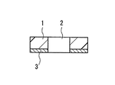
本実施の形態における固体撮像装置は、基台1に付設された配線3の構造が従来例と相違する。基台1は、絶縁性の材料、例えばエポキシ樹脂等の可塑性樹脂からなり、平面形状が中央部に矩形の開口部2を有する矩形枠状である。基台1の断面形状は、全体として実質的に一様な厚みを有する平板状である。基台1の下面には、開口部2の周縁から基台1の外周端に亘って、金属薄板リードからなる複数本の配線3が配置されている。金属薄板リードとしては、通常のリードフレームに使用される材料と同様な、例えばCu合金、42アロイ(Fe-Ni42合金)等が用られ、厚さは概ね2〜3μmである。
【0021】
基台1における配線3が形成された面に、Si基板に形成されたCCD等の撮像素子4が固定され、その電極が配線3と接続されている。各配線3における開口部2に隣接した端部が内部端子部3aを形成し、バンプ7を介して撮像素子4の電極パッドと接続されている。各配線3における、基台1の外周端部の下面に配置された部分が外部端子部3bを形成し、回路基板上の電極と接続するために用いられる。
【0022】
基台1は、各配線3を構成する複数本の金属薄板リードを樹脂に埋め込んで成形されている。配線3を構成する金属薄板リードが埋め込まれた基台1の構造を、図2を参照して説明する。図2(a)は、図1の下方から見た、撮像素子4が実装される前の状態の基台1を示す平面図である。図2(b)はその側面図である。
【0023】
図2(a)に示すように、配線3は、下側表面の全体が露出している。一方、図2(b)に示すように、配線3の端面は、基台1を形成する樹脂中に埋め込まれている。したがって、基台1の枠形状が金属薄板リードにより補強され、上下面の平坦度が良好である。すなわち、金属薄板リードが埋め込まれることにより、捩れや反りを発生させる内部応力に抗するように剛性が高められ、枠形状の平坦度が維持される。その結果、基台1の面に搭載された撮像素子4の位置が安定し、受光領域4aに対して鏡筒を精度良く位置決めすることが容易である。配線3の端面は、必ずしも図示するように全て埋め込まれる必要はない。埋め込まれる程度は、本実施の形態の作用・効果を得るために十分であれば、他の条件に応じて調整可能である。
【0024】
また、金属薄板リードは、金属薄板の切断加工により寸法精度よく、かつばらつきが少なく、しかも低コストで製造することができる。
【0025】
基台1には、複数個の位置決め孔9(2個を図示)が形成されている。位置決め孔9は、同心状に形成された、上面側の大径部9aと下面側の小径部9bとからなる。図2(a)に示されるように、位置決め孔9は配線3と重ならないように配置され、小径部9bが裏面に露出する。この小径部9bの位置を画像認識装置等により検出し、小径部9bの位置を基準にして、撮像素子4を実装する際の位置決めを行うことができる。さらに、鏡筒の平面位置の位置決めを大径部9aを基準にして行えば、撮像素子4と鏡筒を互いに精度よく位置決めすることが可能である。鏡筒の位置決めは、例えば、鏡筒の下部に設けた軸部を、大径部9aに嵌合させることにより、簡単に行うことができる。
【0026】
図示されるように、複数個の位置決め孔9を、基台1の平面形状における非対称な位置に配置するとよい。それにより、基台1の方向認識にも用いることができる。また、互いに径を異ならせて複数個の位置決め孔を配置しても、同様な効果を得ることができる。
【0027】
上述のように基台1を平坦な板状とすることにより、樹脂成形が容易であることに加えて、次のような利点が得られる。すなわち、樹脂成形の後、基台1の平坦度をさらに向上させるため、基台1の変形を矯正する工程を施すことが可能である。
【0028】
本実施の形態における固体撮像装置の製造方法は、上述の構成を有する固体撮像装置の製造に際して、複数個の基台を一度に、かつ良好な平坦度で形成する工程を備えたものである。この製造方法について、図3および図4を参照して説明する。
【0029】
まず、図3(a)に示すように、金属薄板リード10を有するリードフレームを担持したテープ材11を用意する。各金属薄板リード10は、上述の固体撮像装置における配線3を形成するように、本数、寸法、および配置が設定されている。また、複数の固体撮像装置を形成する複数の基台に対応させて、複数組の金属薄板リード10が配置される。
【0030】
次に、図3(b)に示すように、下金型12と上金型13を、テープ材11を挟んで対向させる。上金型13には、複数個の基台1に相当する空間を形成する凹部13aが設けられている。凹部13a中に、基台1の開口部2に相当する複数個の凸部13bが形成されている。したがって、凹部13aと凸部13bにより、開口部2を含む基台1の形状に相当するキャビティが形成される。上金型13にはさらに、基台1の位置決め孔9を形成するためのピン14が設けられている。テープ材11は、その上に担持された各金属薄板リード10が各キャビティ内で適切に配置されるように位置決めされる。この状態で、上金型13の凸部13bおよびピン14の先端部がテープ材11に食い込むように、金型12、13、ピン14、およびテープ材11の寸法を設定するとよい。それにより、樹脂成形後にテープ材11を除去する際に、成形バリが、テープ材11に付着して除去されるようにすることができる。
【0031】
下金型12と上金型13間に形成されるキャビティに樹脂を充填し、硬化させた後、下金型12と上金型13を開いて、図3(c)に示す樹脂成型体15を取り出す。樹脂成型体15には、下面に金属薄板リード10が埋め込まれている。
【0032】
この状態で、図3(d)に示すように、金属薄板リード10が埋め込まれた樹脂成型体15を、加熱条件下で、一対の平坦な平行面金型16、17で押圧する。それにより、樹脂成型体15の反りを低減するための矯正キュアが施される。他の種々の条件により変わるが、概ね、加熱温度は100〜200℃の範囲、圧力は1〜30kgの範囲で選択すれば、良好な結果が得られた。
【0033】
次に、図3(e)に示すように、テープ材11を剥離する。さらに、図3(f)に示すように、ダイシングソー18を用いて個片に分離することにより、図4に示すように基台1が得られる。この基台1に、図1に示すように撮像素子4を実装し、透明板5を固定して、固体撮像装置が作成される。
【0034】
上述の成形工程において、リードフレームを用いて樹脂成型体15に金属薄板リード10を埋め込むことにより、基台1の捩れや反りを生じることが抑制される。それでもなお多少発生する捩れや反りを、図3(d)の矯正キュアの工程により低減させて、さらに平坦度を高めた基台1を得ることができる。成形直後の樹脂成型体15に捩れや反りが少なく、実用的に十分な平坦度が得られれば、矯正キュアの工程は必須ではない。
【0035】
(実施の形態2)
図5を参照して、実施の形態2における固体撮像装置の製造方法について説明する。この実施の形態は、基台を成形するための金型の構成が、実施の形態1の方法と相違する。
【0036】
まず、図5(a)に示すように、金属薄板リード10を有するリードフレームを担持したテープ材11を用意する。本実施の形態においては、テープ材11上に更に、金属薄板リード10とともにブロック材19が担持されている。ブロック材19は、Cu系材、Fe系材、Al材等からなり、基台1の開口部2を形成するために用いられる。
【0037】
次に、図5(b)に示すように、下金型12と上金型13を、テープ材11を挟んで対向させる。上金型13には、矩形板状の空間を形成する凹部13cが設けられている。凹部13c中に、複数個のブロック材19が配置されることにより、凹部13c内に、開口部2を含む基台1の形状に相当するキャビティが複数個形成される。テープ材11は、その上に担持された各金属薄板リード10がキャビティ内で適切に配置されるように位置決めされる。凹部13c内でのブロック材19に対する各金属薄板リード10の位置決めは、テープ材11上でなされている。
【0038】
凹部13cとブロック材19により形成されるキャビティに樹脂を充填し、硬化させた後、下金型12と上金型13を開いて、図5(c)に示す樹脂成型体15を取り出す。樹脂成型体15には、下面に金属薄板リード10が埋め込まれている。この段階では、開口部2に相当する部分にブロック材19が配置された状態を保持する。
【0039】
この状態で、図5(d)に示すように、金属薄板リード10が埋め込まれた樹脂成型体15を、加熱条件下で、一対の平坦な平行面金型16、17で押圧する。それにより、樹脂成型体15の反りを低減するための矯正キュアが施される。
【0040】
次に、図5(e)に示すように、テープ材11を剥離し、ブロック材19を抜き取る。さらに、図5(f)に示すように、ダイシングソー18を用いて個片に分離することにより、図4に示したような基台1が得られる。この基台1に、図1に示すように撮像素子4を実装し、透明板5を固定して、固体撮像装置が作成される。
【0041】
上述の成形工程において、リードフレームを用いて樹脂成型体15に金属薄板リード10を埋め込むことにより、基台1の捩れや反りを生じることが抑制される。それでもなお多少発生する捩れや反りを、図5(d)の矯正キュアの工程により低減させて、さらに平坦度を高めた基台1を得ることができる。成形直後の樹脂成型体15に捩れや反りが少なく、実用的に十分な平坦度が得られれば、矯正キュアの工程は必須ではない。
【0042】
(実施の形態3)
実施の形態3における固体撮像装置の製造方法について、図6〜図8を参照して説明する。本実施の形態の製造方法は、図6に示すような構造の固体撮像装置に適用される。この構造は、図1に示した実施の形態1の場合と概ね同一である。実施の形態1との相違点は、基台21の開口部22に面した内端面21aの断面形状である。内端面21aは、基台21の上下面に対して直交せず、所定の傾きを持っている。具体的には、基台21の撮像素子4側の面と内端面21aが成す角が、90°より大きくなる向きに内端面21aが傾斜している。内端面21aがこのような傾斜を持つことにより、受光領域4aへの入射光に対する、内端面21aによる不都合な反射が軽減される。上記の傾斜角度は、90°〜1200°の範囲とすることが望ましい。
【0043】
この構成を有する固体撮像装置を製造する方法について、図7を参照して説明する。この製造方法は、実施の形態2の方法に用いるブロック材19の形状を変更したものである。
【0044】
まず、図7(a)に示すように、金属薄板リード10を有するリードフレームと、ブロック材23を担持したテープ材11を用意する。ブロック材23は、実施の形態1の場合と同様の材料からなり、基台21の開口部22を形成するために用いられる。ブロック材23の端面は、テープ材11の側の底面となす角が90°より小さくなる向きに傾斜している。
【0045】
次に、図7(b)に示すように、下金型24と上金型25を、テープ材11を挟んで対向させる。上金型25には、矩形板状の空間を形成する凹部25aが設けられている。凹部25a中にブロック材22が配置されことにより、凹部25a内に、開口部22を含む基台21の形状に相当するキャビティが形成される。凹部25a内でのブロック材23に対する各金属薄板リード10の位置決めは、テープ材11上でなされている。
【0046】
凹部25aにより形成されるキャビティに樹脂を充填し、硬化させた後、下金型24と上金型25を開いて、図7(c)に示す樹脂成型体26を取り出す。樹脂成型体26には、下面に金属薄板リード10が埋め込まれている。この段階では、開口部22に相当する部分にブロック材23が配置された状態を保持する。
【0047】
この状態で、図7(d)に示すように、金属薄板リード10が埋め込まれた樹脂成型体26を、加熱条件下で、一対の平坦な平行面金型27、28で押圧する。それにより、樹脂成型体26の反りを低減するための矯正キュアが施される。次に、図7(e)に示すように、テープ材11を剥離し、ブロック材23を抜き取る。さらに、図7(f)に示すように、ダイシングソー18を用いて個片に分離することにより、図8に示すように基台21が得られる。この基台21に、図6に示すように撮像素子4を実装し、透明板5を固定して、固体撮像装置が作成される。
【0048】
上述の成形工程において、樹脂成型体26に金属薄板リード10を埋め込むこと、および図7(d)の矯正キュアの工程により、基台21の捩れや反りを軽減して、平坦度の高い基台21が得られることは、実施の形態1と同様である。さらに本実施の形態によれば、図6に示したような、基台21の内端面21aに傾斜を持たせることが容易である。
【0049】
なお、上述の説明では、複数個の基台を同時に成形する例を示したが、1個の基台を成形する場合でも、各実施の形態の技術を適用可能である。
【0050】
【発明の効果】
本発明の固体撮像装置の製造方法によれば、撮像素子を搭載する基台の剛性が、配線に用いられる金属薄板リードにより高められ、併せて矯正キュアの工程を採用することにより、基台が実用的に十分な平坦度を有する固体撮像装置を得ることができる。
【図面の簡単な説明】
【図1】 実施の形態1における固体撮像装置の断面図
【図2】 図1の固体撮像装置を構成する基台の構造を示し、(a)は裏面から見た平面図、(b)は側面図
【図3】 図1の固体撮像装置を製造するための工程を示す断面図
【図4】 図3の工程により製造された基台を示す断面図
【図5】 図1の固体撮像装置を製造するための実施の形態2における製造方法の工程を示す断面図
【図6】 実施の形態3における固体撮像装置の断面図
【図7】 図6の固体撮像装置を製造するための工程を示す断面図
【図8】 図7の工程により製造された基台を示す断面図
【図9】 従来例の固体撮像装置の断面図
【符号の説明】
1、21、31 基台
2、22、32 開口部
3、33 配線
3a、33a 内部端子部
3b、33b 外部端子部
4 撮像素子
4a 受光領域
5 透光板
6 シール樹脂
7 バンプ
8 はんだボール
10 金属薄板リード
11 テープ材
12 下金型
13 上金型
13a、13c 凹部
13b 凸部
14 ピン
15 樹脂成型体
16、17 平行面金型
18 ダイシングソー
19 ブロック材
21a 内端面
23 ブロック材
24 下金型
25 上金型
25a 凹部
26 樹脂成型体
27、28 平行面金型[0001]
BACKGROUND OF THE INVENTION
The present invention relates to a method for manufacturing a solid-state imaging device configured by mounting an imaging element such as a CCD on a base.
[0002]
[Prior art]
Solid-state imaging devices are widely used in video cameras, still cameras, and the like, and are provided in the form of a package in which an imaging element such as a CCD is mounted on a base made of an insulating material and a light receiving area is covered with a light-transmitting plate. In order to reduce the size of the apparatus, the image pickup device is mounted on the base as a bare chip (see, for example, Patent Document 1). A conventional example of such a solid-state imaging device will be described with reference to FIG.
[0003]
The base 31 in FIG. 9 is a frame having a plane shape with an
[0004]
An electrode pad (not shown) connected to the circuit of the
[0005]
This solid-state imaging device is mounted on a circuit board with the light-transmitting
[0006]
A lens barrel (not shown) in which an imaging optical system is incorporated is mounted on the upper part of the
[0007]
[Patent Document 1]
Japanese Patent Laid-Open No. 2002-43554
[Problems to be solved by the invention]
However, it is difficult to obtain a sufficient flatness of the base 31 in the configuration of the above-described conventional solid-state imaging device. That is, since the
[0009]
Further, although not described in
[0010]
An object of the present invention is to provide a manufacturing method capable of efficiently forming a plurality of bases for mounting an image pickup device at once with practically sufficient flatness. It is another object of the present invention to provide a method for manufacturing a solid-state imaging device that can be provided with wiring at low cost with little variation in dimensional accuracy.
[0011]
[Means for Solving the Problems]
A manufacturing method of a solid-state imaging device according to the present invention includes a base made of an insulating material having a frame-like planar shape with an opening formed in an inner region, and a substantially uniform thickness. A wiring attached to one surface so as to extend from the opening side toward the outside, and an imaging mounted on the attachment surface of the wiring on the base so that a light receiving region faces the opening. And the wiring has an internal terminal portion located on the opening side and an external terminal portion located on the outer peripheral portion of the base, and the electrode of the imaging element and the internal terminal portion are electrically This is a method for manufacturing a solid-state imaging device connected to the.
[0012]
In order to solve the above problems, a manufacturing method of the present invention includes a pair of molds forming a cavity for resin-molding a plurality of the bases, and a plurality of sets corresponding to the plurality of bases. A tape material carrying a thin metal plate lead for forming wiring, and the mold is provided with a plurality of pins for forming a plurality of positioning holes in the thickness direction of the base. The tape material is loaded between the molds, and each set of the thin metal plate leads is disposed in the region corresponding to the plurality of bases in the cavity, and the cavity is filled with a sealing resin and cured. The resin molded body in which the metal thin plate lead is embedded is taken out of the mold, the tape material is removed from the resin molded body, and the resin molded body corresponds to the base on which the wiring is attached. Separated into multiple pieces, front Wherein the wiring in the base to implement the imaging element attached to the surface.
[0013]
DETAILED DESCRIPTION OF THE INVENTION
According to the method for manufacturing a solid-state imaging device of the present invention, a pair of molds that form cavities for resin-molding a plurality of bases, and a metal that forms a plurality of sets of wires corresponding to the plurality of bases By using the tape material supporting the thin plate lead and embedding the thin metal plate lead in the base forming process, the base is prevented from being twisted or warped.
[0014]
The flatness of the base is further improved by pressing the resin molded body taken out from the mold between the flat molds that form a pair of parallel surfaces under heating conditions, and performing straightening cure. Can do. Since the base formed by the above method does not substantially have an uneven shape, it is suitable for performing correction curing.
Moreover, a convex part is provided in one of a pair of metal mold | die so that it may be located in the cavity formed with a pair of metal mold | die, and the opening part of a base can be formed with the convex part of the metal mold | die.
[0015]
In the above manufacturing method, in order to form the cavity, a pair of molds and a block material for forming an opening of the base placed between the pair of molds can be used. After filling the cavity with sealing resin and curing it, the resin molded body in which the thin metal plate lead is embedded and the block material is held is taken out of the mold, and the tape material and the block material are removed from the resin molded body, The resin molding is separated into a plurality of pieces each corresponding to a base provided with wiring. Preferably, after the resin molded body holding the block material is taken out of the mold, correction curing is performed by pressing between the flat molds forming a pair of parallel surfaces under heating conditions.
[0016]
In the manufacturing method described above, the block material is supported on the tape material together with the thin metal plate lead, the tape material is sandwiched between a pair of molds to form a cavity, and the thin metal plate lead is disposed in the cavity. May be. In that case, it is preferable that the end surface of the block material is inclined in a direction in which an angle formed with the bottom surface on the tape material side is smaller than 90 degrees. According to this, it is easy to incline the end surface on the opening side of the base, and the reflection of incident light to the light receiving region can be adjusted to a range that does not substantially adversely affect the imaging function.
[0017]
In the manufacturing method described above, the molding burr of the resin molded body is preferably removed by adhering to the tape material when the tape material is removed from the resin molded body. To that end, when loaded with tape material between the pair of molds, of the mold tip or plurality of pin of the convex portion of the to form an opening of the base, at least one of the distal portion but to bite into the tape material, a pair of molds, a plurality of pins, it is preferable to set the size of your and tape material.
Alternatively, when the tape material is loaded between the pair of molds, the pair of molds and the plurality of pins are arranged such that at least one tip portion of the plurality of pins or block materials bites into the tape material. It is preferable to set the dimensions of the block material and the tape material.
[0018]
Embodiments of the present invention will be specifically described below with reference to the drawings.
[0019]
(Embodiment 1)
A method of manufacturing the solid-state imaging device according to
[0020]
The solid-state imaging device according to the present embodiment is different from the conventional example in the structure of the
[0021]
An
[0022]
The
[0023]
As shown in FIG. 2A, the entire lower surface of the
[0024]
Further, the thin metal plate lead can be manufactured with high dimensional accuracy, little variation, and low cost by cutting the thin metal plate.
[0025]
A plurality of positioning holes 9 (two shown) are formed in the
[0026]
As illustrated, the plurality of positioning holes 9 may be disposed at asymmetric positions in the planar shape of the
[0027]
By making the
[0028]
The manufacturing method of the solid-state imaging device according to the present embodiment includes a step of forming a plurality of bases at a time with good flatness when manufacturing the solid-state imaging device having the above-described configuration. This manufacturing method will be described with reference to FIGS.
[0029]
First, as shown in FIG. 3A, a
[0030]
Next, as shown in FIG. 3B, the
[0031]
A resin formed in a cavity formed between the
[0032]
In this state, as shown in FIG. 3D, the resin molded
[0033]
Next, as shown in FIG. 3E, the
[0034]
In the above-described molding process, the
[0035]
(Embodiment 2)
With reference to FIG. 5, the manufacturing method of the solid-state imaging device in
[0036]
First, as shown in FIG. 5A, a
[0037]
Next, as shown in FIG. 5B, the
[0038]
After the resin formed in the cavity formed by the
[0039]
In this state, as shown in FIG. 5D, the resin molded
[0040]
Next, as shown in FIG. 5E, the
[0041]
In the above-described molding process, the
[0042]
(Embodiment 3)
A method of manufacturing the solid-state imaging device according to
[0043]
A method of manufacturing a solid-state imaging device having this configuration will be described with reference to FIG. This manufacturing method changes the shape of the
[0044]
First, as shown in FIG. 7A, a lead frame having a thin
[0045]
Next, as shown in FIG. 7B, the
[0046]
After the resin formed in the cavity formed by the
[0047]
In this state, as shown in FIG. 7D, the resin molded
[0048]
In the above-described molding step, the
[0049]
In the above description, an example in which a plurality of bases are formed at the same time has been shown. However, the technology of each embodiment can be applied even when a single base is formed.
[0050]
【The invention's effect】
According to the method for manufacturing a solid-state imaging device of the present invention, the rigidity of the base on which the imaging element is mounted is enhanced by the metal thin plate lead used for wiring, and the base is fixed by adopting a correction curing process. A solid-state imaging device having practically sufficient flatness can be obtained.
[Brief description of the drawings]
1 is a cross-sectional view of a solid-state imaging device in
1, 21, 31
Claims (11)
複数個の前記基台を樹脂成形するためのキャビティを形成する一対の金型と、複数個の前記基台に対応する複数組の前記配線を形成するための金属薄板リードを担持するテープ材とを用い、前記金型には、前記基台の厚さ方向の位置決め孔を複数形成するための複数個のピンを設け、
前記一対の金型の間に前記テープ材を装填して、前記キャビティにおける前記複数の基台に対応する領域に各々、各組の前記金属薄板リードを配置し、
前記キャビティに封止樹脂を充填して硬化させ、
前記金属薄板リードが埋め込まれた樹脂成型体を前記金型から取り出し、
前記テープ材を前記樹脂成型体から除去し、
前記樹脂成型体を前記配線が付設された前記基台に各々対応する複数の個片に分離し、
前記基台における前記配線が付設された面に前記撮像素子を実装することを特徴とする固体撮像装置の製造方法。A base made of an insulating material having a frame-like planar shape with an opening formed in the inner region and a substantially uniform thickness, and on one surface of the base from the opening side to the outside A wiring provided so as to extend toward the surface, and an imaging element mounted on a surface of the base on which the wiring is provided so that a light receiving region faces the opening. The wiring includes the opening. A solid-state imaging device having an internal terminal portion positioned on the side and an external terminal portion positioned on an outer peripheral portion of the base, wherein the electrode of the imaging element and the internal terminal portion are electrically connected In
A pair of molds forming cavities for resin-molding a plurality of bases, and a tape material carrying metal thin plate leads for forming a plurality of sets of wirings corresponding to the plurality of bases; The mold is provided with a plurality of pins for forming a plurality of positioning holes in the thickness direction of the base,
The tape material is loaded between the pair of molds, and each set of the thin metal plate leads is disposed in a region corresponding to the plurality of bases in the cavity,
Fill the cavity with sealing resin and cure,
Take out the resin molding in which the thin metal plate lead is embedded from the mold,
Removing the tape material from the molded resin,
Separating the resin molding into a plurality of pieces each corresponding to the base to which the wiring is attached;
A method of manufacturing a solid-state imaging device, wherein the imaging element is mounted on a surface of the base on which the wiring is attached.
前記キャビティに封止樹脂を充填して硬化させた後、前記金属薄板リードが埋め込まれ、かつ前記ブロック材が保持された樹脂成型体を前記金型から取り出し、
前記テープ材および前記ブロック材を前記樹脂成型体から除去し、
前記樹脂成型体を前記配線が付設された前記基台に各々対応する複数の個片に分離する請求項1に記載の固体撮像装置の製造方法。In order to form the cavity, a pair of molds and a block material for forming the opening of the base placed between the pair of molds,
After the cavity is filled with a sealing resin and cured, the resin thin body in which the metal thin plate lead is embedded and the block material is held is taken out from the mold,
Removing the tape material and the block material from the resin molding,
The method of manufacturing a solid-state imaging device according to claim 1, wherein the resin molded body is separated into a plurality of pieces each corresponding to the base to which the wiring is attached.
前記一対の金型の間に前記テープ材を挟み込んで、前記キャビティを形成するとともに、前記キャビティ内に前記金属薄板リードを配置する請求項4に記載の固体撮像装置の製造方法。The tape material is supported on the tape material together with the metal thin plate lead,
The manufacturing method of the solid-state imaging device according to claim 4 , wherein the tape material is sandwiched between the pair of molds to form the cavity, and the metal thin plate lead is disposed in the cavity.
Priority Applications (7)
| Application Number | Priority Date | Filing Date | Title |
|---|---|---|---|
| JP2003123842A JP3729817B2 (en) | 2003-04-28 | 2003-04-28 | Method for manufacturing solid-state imaging device |
| TW092126171A TW200423389A (en) | 2003-04-28 | 2003-09-23 | Manufacturing method of solid-state photographing apparatus |
| DE60316664T DE60316664T2 (en) | 2003-04-28 | 2003-09-24 | Method for producing a solid state image pickup device |
| US10/669,229 US6864117B2 (en) | 2003-04-28 | 2003-09-24 | Method for producing solid-state imaging device |
| EP03021542A EP1473775B1 (en) | 2003-04-28 | 2003-09-24 | Method for producing solid-state imaging device |
| CNB031598366A CN100401522C (en) | 2003-04-28 | 2003-09-26 | Method for producing solid-state imaging device |
| KR1020030067841A KR100576765B1 (en) | 2003-04-28 | 2003-09-30 | Method for manufacturing solid state imaging device |
Applications Claiming Priority (1)
| Application Number | Priority Date | Filing Date | Title |
|---|---|---|---|
| JP2003123842A JP3729817B2 (en) | 2003-04-28 | 2003-04-28 | Method for manufacturing solid-state imaging device |
Publications (2)
| Publication Number | Publication Date |
|---|---|
| JP2004327917A JP2004327917A (en) | 2004-11-18 |
| JP3729817B2 true JP3729817B2 (en) | 2005-12-21 |
Family
ID=32985561
Family Applications (1)
| Application Number | Title | Priority Date | Filing Date |
|---|---|---|---|
| JP2003123842A Expired - Fee Related JP3729817B2 (en) | 2003-04-28 | 2003-04-28 | Method for manufacturing solid-state imaging device |
Country Status (7)
| Country | Link |
|---|---|
| US (1) | US6864117B2 (en) |
| EP (1) | EP1473775B1 (en) |
| JP (1) | JP3729817B2 (en) |
| KR (1) | KR100576765B1 (en) |
| CN (1) | CN100401522C (en) |
| DE (1) | DE60316664T2 (en) |
| TW (1) | TW200423389A (en) |
Families Citing this family (14)
| Publication number | Priority date | Publication date | Assignee | Title |
|---|---|---|---|---|
| JP4180537B2 (en) * | 2003-10-31 | 2008-11-12 | シャープ株式会社 | Optical element sealing structure, optical coupler, and optical element sealing method |
| JP4324081B2 (en) * | 2004-11-22 | 2009-09-02 | パナソニック株式会社 | Optical device |
| JP4196937B2 (en) * | 2004-11-22 | 2008-12-17 | パナソニック株式会社 | Optical device |
| JP4290134B2 (en) * | 2005-03-14 | 2009-07-01 | パナソニック株式会社 | Solid-state imaging device and method for manufacturing solid-state imaging device |
| JP4595835B2 (en) * | 2006-03-07 | 2010-12-08 | 株式会社日立製作所 | Leaded electronic parts using lead-free solder |
| KR100747610B1 (en) * | 2006-04-06 | 2007-08-08 | 삼성전자주식회사 | Image sensor and method of manufacturing the same |
| JP2008243869A (en) * | 2007-03-26 | 2008-10-09 | Tdk Corp | Light-receiving device |
| JP4766435B2 (en) * | 2008-07-24 | 2011-09-07 | Smk株式会社 | Manufacturing method of camera module base |
| JP4693909B2 (en) * | 2009-02-05 | 2011-06-01 | パナソニック株式会社 | Solid-state imaging device and manufacturing method thereof |
| JP5489543B2 (en) * | 2009-06-09 | 2014-05-14 | キヤノン株式会社 | Solid-state imaging device |
| CN103579277B (en) * | 2013-11-14 | 2016-02-03 | 华进半导体封装先导技术研发中心有限公司 | Based on encapsulating structure and the method for packing of upside-down mounting image sensor chip |
| US9666730B2 (en) | 2014-08-18 | 2017-05-30 | Optiz, Inc. | Wire bond sensor package |
| JP2017139258A (en) | 2016-02-01 | 2017-08-10 | ソニー株式会社 | Imaging device package and imaging device |
| JPWO2023053503A1 (en) * | 2021-09-30 | 2023-04-06 |
Family Cites Families (9)
| Publication number | Priority date | Publication date | Assignee | Title |
|---|---|---|---|---|
| US5748658A (en) * | 1993-10-22 | 1998-05-05 | Matsushita Electric Industrial Co., Ltd. | Semiconductor laser device and optical pickup head |
| JP3360504B2 (en) * | 1995-11-10 | 2002-12-24 | ソニー株式会社 | Post-processing method and manufacturing method of solid-state imaging device |
| JP4372241B2 (en) | 1998-08-05 | 2009-11-25 | パナソニック株式会社 | Method for manufacturing solid-state imaging device |
| US6753922B1 (en) * | 1998-10-13 | 2004-06-22 | Intel Corporation | Image sensor mounted by mass reflow |
| US6147389A (en) * | 1999-06-04 | 2000-11-14 | Silicon Film Technologies, Inc. | Image sensor package with image plane reference |
| JP3461332B2 (en) * | 1999-09-10 | 2003-10-27 | 松下電器産業株式会社 | Lead frame, resin package and optoelectronic device using the same |
| TW454309B (en) | 2000-07-17 | 2001-09-11 | Orient Semiconductor Elect Ltd | Package structure of CCD image-capturing chip |
| JP2002043553A (en) * | 2000-07-26 | 2002-02-08 | Canon Inc | Solid-state imaging device |
| JP3540281B2 (en) * | 2001-02-02 | 2004-07-07 | シャープ株式会社 | Imaging device |
-
2003
- 2003-04-28 JP JP2003123842A patent/JP3729817B2/en not_active Expired - Fee Related
- 2003-09-23 TW TW092126171A patent/TW200423389A/en not_active IP Right Cessation
- 2003-09-24 US US10/669,229 patent/US6864117B2/en not_active Expired - Lifetime
- 2003-09-24 EP EP03021542A patent/EP1473775B1/en not_active Expired - Lifetime
- 2003-09-24 DE DE60316664T patent/DE60316664T2/en not_active Expired - Lifetime
- 2003-09-26 CN CNB031598366A patent/CN100401522C/en not_active Expired - Fee Related
- 2003-09-30 KR KR1020030067841A patent/KR100576765B1/en not_active IP Right Cessation
Also Published As
| Publication number | Publication date |
|---|---|
| KR100576765B1 (en) | 2006-05-03 |
| EP1473775B1 (en) | 2007-10-03 |
| DE60316664D1 (en) | 2007-11-15 |
| DE60316664T2 (en) | 2008-02-07 |
| US20040214369A1 (en) | 2004-10-28 |
| CN1542983A (en) | 2004-11-03 |
| TWI309084B (en) | 2009-04-21 |
| US6864117B2 (en) | 2005-03-08 |
| CN100401522C (en) | 2008-07-09 |
| TW200423389A (en) | 2004-11-01 |
| EP1473775A2 (en) | 2004-11-03 |
| JP2004327917A (en) | 2004-11-18 |
| EP1473775A3 (en) | 2006-01-11 |
| KR20040093361A (en) | 2004-11-05 |
Similar Documents
| Publication | Publication Date | Title |
|---|---|---|
| JP3768972B2 (en) | Solid-state imaging device and manufacturing method thereof | |
| JP3782405B2 (en) | Solid-state imaging device and manufacturing method thereof | |
| JP3729817B2 (en) | Method for manufacturing solid-state imaging device | |
| KR101378418B1 (en) | image sensor module and fabrication method thereof | |
| JP3782406B2 (en) | Solid-state imaging device and manufacturing method thereof | |
| JP4606063B2 (en) | Optical device and manufacturing method thereof | |
| JP3838572B2 (en) | Solid-state imaging device and manufacturing method thereof | |
| JP3898666B2 (en) | Solid-state imaging device and manufacturing method thereof | |
| JP4486005B2 (en) | Semiconductor imaging device and manufacturing method thereof | |
| CN101047195A (en) | Semiconductor imaging device and method for manufacturing the same | |
| JP2007317719A (en) | Imaging device and its manufacturing method | |
| JP3838573B2 (en) | Solid-state imaging device | |
| JP2009188191A (en) | Semiconductor device and manufacturing method thereof | |
| JP4219943B2 (en) | Solid-state imaging device | |
| JPH03155671A (en) | Solid-state image sensing device | |
| JP2006245359A (en) | Photoelectric conversion device, and manufacturing method thereof | |
| JP2006332686A (en) | Solid-state imaging device | |
| JP3713026B2 (en) | Method for manufacturing solid-state imaging device | |
| JP2005142334A (en) | Premolding type semiconductor package and semiconductor device using same | |
| JP2009278024A (en) | Semiconductor device | |
| JP2010135821A (en) | Semiconductor imaging device and method of manufacturing same |
Legal Events
| Date | Code | Title | Description |
|---|---|---|---|
| A977 | Report on retrieval |
Free format text: JAPANESE INTERMEDIATE CODE: A971007 Effective date: 20050622 |
|
| A131 | Notification of reasons for refusal |
Free format text: JAPANESE INTERMEDIATE CODE: A131 Effective date: 20050628 |
|
| A521 | Request for written amendment filed |
Free format text: JAPANESE INTERMEDIATE CODE: A523 Effective date: 20050823 |
|
| TRDD | Decision of grant or rejection written | ||
| A01 | Written decision to grant a patent or to grant a registration (utility model) |
Free format text: JAPANESE INTERMEDIATE CODE: A01 Effective date: 20050922 |
|
| A61 | First payment of annual fees (during grant procedure) |
Free format text: JAPANESE INTERMEDIATE CODE: A61 Effective date: 20051004 |
|
| R150 | Certificate of patent or registration of utility model |
Free format text: JAPANESE INTERMEDIATE CODE: R150 |
|
| FPAY | Renewal fee payment (event date is renewal date of database) |
Free format text: PAYMENT UNTIL: 20091014 Year of fee payment: 4 |
|
| FPAY | Renewal fee payment (event date is renewal date of database) |
Free format text: PAYMENT UNTIL: 20091014 Year of fee payment: 4 |
|
| FPAY | Renewal fee payment (event date is renewal date of database) |
Free format text: PAYMENT UNTIL: 20101014 Year of fee payment: 5 |
|
| FPAY | Renewal fee payment (event date is renewal date of database) |
Free format text: PAYMENT UNTIL: 20111014 Year of fee payment: 6 |
|
| FPAY | Renewal fee payment (event date is renewal date of database) |
Free format text: PAYMENT UNTIL: 20121014 Year of fee payment: 7 |
|
| FPAY | Renewal fee payment (event date is renewal date of database) |
Free format text: PAYMENT UNTIL: 20131014 Year of fee payment: 8 |
|
| S533 | Written request for registration of change of name |
Free format text: JAPANESE INTERMEDIATE CODE: R313533 |
|
| R350 | Written notification of registration of transfer |
Free format text: JAPANESE INTERMEDIATE CODE: R350 |
|
| S111 | Request for change of ownership or part of ownership |
Free format text: JAPANESE INTERMEDIATE CODE: R313113 |
|
| R250 | Receipt of annual fees |
Free format text: JAPANESE INTERMEDIATE CODE: R250 |
|
| R250 | Receipt of annual fees |
Free format text: JAPANESE INTERMEDIATE CODE: R250 |
|
| LAPS | Cancellation because of no payment of annual fees |