Optical head and manufacture method thereof, optical recording/reproducing apparatus
Technical field
The present invention relates to a kind of laser module or optical head.For example, the present invention relates to a kind of following laser module or optical head: wherein, one is applied on the optical information recording media of CD and so on by electric signal Modulated Semiconductor Laser bundle, so as on these medium recorded information or from these medium the information of reproducing recorded.Especially, the present invention relates to a kind of laser module or optical head that uses a plurality of light sources.
Background technology
In the optical head on being loaded on video disc recording and readout equipment, light source and photoelectric detector are separated from one another.Therefore, the height that can not reach light source and photoelectric detector is made integration density, thereby can not realize reducing the size and the thickness of overall optical disc apparatus so far.In the work that addresses this problem, attempting mixing the photoelectric detector and the semiconductor laser of the integrated optical disc replay head in ground till now always, intend among the flat 1-150244 of publication number disclosed as Jap.P..
Recently, developing a kind of compact disk equipment that can play CD of all kinds always, CD, CD-ROM, CD-R and CD-that the specification of these CDs includes the 780nm wavelength can rewrite specification, with the DVD that the 650nm wavelength is arranged, DVD-ROM and DVD-RAM specification, yet for the semiconductor laser of different wave length, its light source separates with photoelectric detector.In addition, to use in the future blue look, purple or even can improve the more short wavelength's of recording density laser more.Like this, can increase part count in the optical head inevitably.In these cases, the size and the thickness of wishing the entire equipment of video disc recording and readout equipment and so on further reduces.
Summary of the invention
One object of the present invention is to improve the problems referred to above.More particularly, the object of the present invention is to provide an important invention, so that, reduce its size and thickness to writing down and reproduce the whole driver of various optical disc informations.
The invention provides a kind of optical head, it is characterized in that, partly removed in the groove that forms in its surperficial substrate at one, install one and have first LASER Light Source and second LASER Light Source that is used to read or write down from first vibration wavelength of the data of recording medium with second vibration wavelength that is different from first vibration wavelength or becomes first vibration wavelength; Reflected by a catoptron that constitutes a part of described groove from the described first and second LASER Light Source emitted laser bundles, and on the normal direction of a substrate surface or in a direction of leaving from substrate surface, export; One first photo-detector device is provided, is used for obtaining the out of focus detection signal according in the laser beam of returning later on by described recording medium surface reflection; One second photo-detector device is used to obtain a tracking error detection signal and an information regeneration signal; With one the 3rd photo-detector device, be used to monitor light quantity from the light of first or second LASER Light Source emission; And in described first photo-detector device, be used for according to from the device of the laser beam detection out of focus detection signal of first LASER Light Source be used for separating each other according to device from the laser beam detection out of focus detection signal of second LASER Light Source.
The invention provides a kind of method that is used to make optical head, it is characterized in that, comprise the steps: on a substrate, integrally to form one first photo-detector device, be used to obtain the out of focus detection signal; One second photo-detector device is used to obtain tracking error detection signal and information regeneration signal; With one the 3rd photo-detector device, be used to monitor light quantity from the emission of first or second LASER Light Source; Divide ground to form a groove in an interior surface of described substrate, described groove has an inclined-plane that plays the catoptron effect of reflection lasering beam; And first LASER Light Source with first vibration wavelength is installed in described groove and has second LASER Light Source of second vibration wavelength that is different from first vibration wavelength; And described first photoelectric detection system is made into to be used for according to the device of the laser beam detection out of focus detection signal that sends from described first LASER Light Source and is used for separating each other according to the device of the laser detection out of focus detection signal that sends from described second LASER Light Source.
The invention provides a kind of optical head, be used for information recorded on the CD and information reproduction from the CD, it is characterized in that, described optical head loads an integrated package, described integrated package comprises that a plurality of semiconductor lasers that different wave length arranged and one are useful on photoelectric detector that the automatic focus detection and tracking detect and are integrally formed in semiconductor chip on it, described photoelectric detector has the sensitivity on respective wavelength, and one of them alignment mark is additional on one of described semiconductor laser and described semiconductor chip the two or the two.
First device that adopts according to the present invention, the various semiconductor lasers that produce different wave length are calibrated with the photoelectric detector that is equivalent to these different wave lengths, to have the precision of sheltering; Then according to mixing the integrated a plurality of semiconductor lasers of integration mode, equal the degree that monolithic disposes so that the number of parts is reduced to.In addition, according to first device, though use a plurality of light paths in conventional optical head, an independent light path is suitable therewith.
Second device that adopts according to the present invention, have on the photoelectric detector silicon chip formed thereon and semiconductor laser on more additional scale marks that are used to calibrate, their image is formed on the opto-electronic conversion surface of CCD and so on, in the input computing machine, the centre of form and the calibration of calculating mark then.Centroid calculation is allowed the calibration accuracy that guarantees submicron order.
The 3rd device that adopts according to the present invention is having catoptron of formation on the photoelectric detector silicon chip formed thereon.More precisely, provide a substrate from about axle 9.7 degree, the aeoplotropism etching by silicon forms one 45 catoptron about degree thereon then.By light beam that sends from semiconductor laser of this mirror reflection, this light beam is bent near on the direction perpendicular to the silicon chip surface at one.
The 4th device that adopts according to the present invention serves as the width that the basis limits catoptron with the beam spread angle of semiconductor laser.More particularly, the light beam that sends from semiconductor laser has an extension width of estimating by Gaussian distribution.If according to intercepting this extensible beam near the semiconductor laser luminous point, Fresnel's diffraction phenomenon takes place then.When the object lens that just in time are positioned at the CD front by form a luminous point, then cause aberration, thereby reduce the center intensity of luminous point.As a result, differentiate the ability drop of CD fovea superior trace, the reproducing signal error takes place.For fear of this trouble, the width of catoptron is configured to, and is wider than the expansion half peaked full duration at the semiconductor laser beam at reflector position place.
The 5th device that adopts according to the present invention is having on the photoelectric detector silicon chip formed thereon, integrally forms an amplifier that is used for electrically amplifying the photocurrent that is produced by photoelectric detector; And on silicon chip, additional tilting mirror calibration scale mark.
The 6th device that adopts according to the present invention combines the above-mentioned second and the 5th device, and according to mixing the integrated a plurality of semiconductor lasers of integration mode and an integrally integrated silicon chip, makes calibration accuracy be higher than the scale mark precision.
The 7th device that adopts according to the present invention is having on the photoelectric detector silicon chip formed thereon, integrally forms an amplifier that is used for electrically amplifying the photocurrent that is produced by photoelectric detector; And have tilting mirror formed thereon and have the calibration indexing marks to add on thereon the silicon chip, during the welding semiconductor laser, between semiconductor laser and silicon chip, insert the material that high heat conductance is arranged, so that expand the heat that produces by semiconductor laser widely.
The 8th device that adopts according to the present invention is having on the photoelectric detector silicon chip formed thereon, integrally forms an amplifier that is used for electrically amplifying the photocurrent that is produced by photoelectric detector; And formed thereon the calibrating on the additional silicon chip thereon of scale mark with having of tilting mirror arranged, during the welding semiconductor laser, between semiconductor laser and silicon chip, insert the material that the stress relief effect is arranged, so that discharge the stress that the difference by thermal expansivity between the two causes.
Description of drawings
Fig. 1 is the figure of optical head that is loaded with the separate optical path of integrated optical source assembly according to one of one embodiment of the invention explanation;
Fig. 2 is the figure of a beam splitting composition element of explanation;
Fig. 3 A and 3B are the structural drawing of the integrated optical source of this embodiment use;
Fig. 4 A, 4B and 4C are the wide figure of mirror that this embodiment of explanation uses;
Fig. 5 A and 5B are the figure of the kit form of explanation integrated optical source;
Fig. 6 A, 6B and 6C are the figure that the integrated optical source of installing on the horizontal plane assembly is described;
Fig. 7 is the integral substrate that explanation is used for integrated optical source, and the figure of calibration calibration, solder flux and electrode pattern;
Fig. 8 is the figure that appends to the calibration calibration figure on the semiconductor laser among this embodiment of explanation;
Fig. 9 is the method key diagram, and this method is used at the calibration semiconductor laser light resource and has calibration between the integral substrate of attached corresponding calibration figure thereon;
Figure 10 is a sectional drawing of taking from A-A ' line among Fig. 3 A;
Figure 11 is the sectional drawing of integral substrate, and this substrate has one and is used to quicken the layer that radiation comes the heat energy of semiconductor laser light resource;
Figure 12 is the key diagram of three kinds of semiconductor laser light resources, is being used for that these light sources are installed on the integral substrate of this embodiment; With
Figure 13 is the key diagram of OEIC (integrated optoelectronic circuit), and this circuit is included in an amplifier and some photoelectric detectors that integrally form on the integral substrate.
Embodiment
Fig. 1 illustrates the configuration of optical head according to the present invention.Integrated package 100 comprises a semiconductor chip 1, semiconductor laser chip 4a and 4b, catoptron 5 and photoelectric detector 7,8,9.With the laser beam from integrated package 100 of collimation lens 10 collimations with 6a and 6b indication, make laser beam pass through mirror 11 and photogate 12 then, arrive object lens 13, thereby make laser beam form CD 14 lip-deep luminous points 15 and 16.Object lens 13 comprise according to a plurality of these class lens of semiconductor laser wavelength and can focus on independent lens of different wave length light beam.These object lens focus on the recording surface of CD according to rotatablely moving of same CD by regulator 17, and follow the tracks of, and, follow a record session 18 that is formed on the optical disc surface that is.Like this,, signal record is become a series of pits on the CD, or read the pit that write down already with reproducing signal according to opening or closing of semiconductor laser.By integrated so a plurality of semiconductor lasers in integrated package 100, make the number of collimation lens 10, the number of object lens 13 and the number of mirror 11 all become 1, light path becomes an independent light path in the optical head thereby can make.Use this optical head, for example can make the semiconductor laser 4a that CD with 1.2mm thickness and CD-R utilize the 780nm wavelength and write down and reproduce, can make the semiconductor laser 4b that DVD with 0.6mm thickness and DVD-RAM utilize 650nm and write down and reproduce.
Fig. 2 illustrates original screen panel 12.This original screen panel is a polarizable grating 23 and the integrally stacking each other composition element that together obtains of quarter wave plate 24 by being divided into 4 parts to.It is arranged to make grating 23 towards the semiconductor laser chip side.Constituted by a birefringence optics crystal or liquid crystal board by four minutes polarizable gratings 23.If incident light is an ordinary ray, then incident light passes it and does not reflect, and if incident light is an extraordinary light, then it plays diffraction grating.As linear polarization light beam 6a and 6b from semiconductor laser 4a and 4b emission, incided and comprised by on the composition element 12 of four fens polarizable gratings and quarter wave plate the time, if these light beams are as ordinary ray incident, then they pass polarizable grating part, become the Circular Polarisation light beam by the quarter wave plate in the composition element 12 then.By CD reflection later laser beam 6a and 6b, become extraordinary light by the quarter wave plate in the composition element, then by four fens polarizable gratings and diffraction.With boundary line 21 and 22 composition element shown in Figure 2 12 is divided into 4 districts.In Fig. 2, circle 20 symbol laser beam 6a or 6b are separated into 4 positive first order diffracted beams and 4 negative first order diffracted beams to it with four fens gratings.The light beam that is separated like this arrives the photoelectric detector 7 or 8 on the semiconductor chip 1, thereby is become automatic focusing signal, tracking signal and information signal by opto-electronic conversion.Describe this point below in detail.
Fig. 3 illustrates the surface of a semiconductor chip 1 of seeing from collimation lens 10 sides.In Fig. 3 A, the λ that the quadrant description of representing with 32a of 8 painted blacks is separated by grating 23
aThe laser beam of wavelength, and 8 λ that the quadrant description of representing with 32b of not tinting is separated by grating
bThe laser beam of wavelength.Be used to obtain the photoelectric detector 7 of an out of focus detection signal, comprise that 8 are used to receive λ
aThe strip optical detection device 7a of the laser beam 32a of wavelength and 8 are used to receive λ
bThe strip optical detection device 7b of the laser beam 32b of wavelength.Make the out of focus detection method with knife-edge method (Foucault method), wherein as shown in Figure 3A, the conductive film thin and so on aluminium connects up, and joint A and the B from wire-bonded sheet 34 obtains differential signal whereby.Photoelectric detector 8 is 4 photoelectric detectors that are used to obtain a tracking error detection signal and an information regeneration signal.From these 4 output signals that photoelectric detector 8 provides, by the amplifier 35 that forms on the semiconductor chip, from joint D, E, F and the G output of joint fastener 34.The output signal that provides from photoelectric detector 9 is from the joint C output of joint fastener 34. Luminous point 31a and 31b represent the catoptron 5 lip-deep reflection units from semi-conductor chip 4a and 4b emitted laser bundle 6a and 6b respectively.For example, the grating space of supposing 4 districts shown in Figure 2 equates mutually, grating orientation with respect to upright position 21 be+α ,-α ,+focal length of 3 α and-3 α degree and collimation lens is f
c, the λ that separates by grating then
aThe laser beam 32a of wavelength be focused on luminous point 31a be the center with R
a=f
c* λ
a/ p is on the circumference of radius, and its position and center separate 2 α degree.Equally, the λ that separates by grating
bThe laser beam 32b of wavelength be focused on luminous point 31b be the center with R
b=f
c* λ
b/ P is on the circumference of radius, and its position and center separate 2 α degree.If the interval D between the luminous point of semiconductor laser chip 4a and 4b, promptly the interval between luminous point 31a and the 31b is D=f
c* (λ
b-λ
a)/p then can make wavelength X
aThe focal position and the wavelength X of laser beam
bThe focal position of laser beam do to overlap mutually basically.Therefore, as present embodiment, photoelectric detector and amplifier can be common to light beams of different wavelengths, thereby not only can save the surface of semiconductor chip 1, also can reduce the number of wire-bonded sheet and output line, the result can reduce the size that semiconductor chip is loaded on shell wherein.
The cross section structure of Fig. 3 B explanation semiconductor chip 1 of dotted line A-A ' position in Fig. 3 A.Preferably, become catoptron 5 with dihedral with respect to 2 one-tenth 45 degree of laser chip installation surface.For example, the processing that is used on silicon chip forming a minute surface is based on anisotropic etching, if thereby use kali aqueous solution etching silicon plane (100), then use plane (111) to make the inclined-plane to form the taper concave part, because with respect to plane (100), the low approximately double figures of the etching speed of plane (111).In this case, plane (111) with respect to plane (100) thus the angle be about 54.7 ° and want shape catoptron at 45, just need to use the silicon chip of the 9.7 ° of fleet angles of having an appointment, wherein crystallographic axis is with respect to surface tilt.Yet, be necessary when determining fleet angle, also consider the applicability of the semiconductor technology that is used to make photoelectric detector and electronic circuit.Catoptron with can move 45 °, perhaps the transmit direction of laser beam 6a or 6b can move from the direction perpendicular to semiconductor chip 1.
Fig. 4 A, 4B and 4C are key diagrams, and how explanation should be provided with the width value of catoptron.In general, shown in Fig. 4 B, expand at an angle from the light beam that semiconductor laser sends, it with respect to the intensity distributions of extended corner near Gaussian distribution.As shown in Fig. 4 A according to configuration of the present invention, near semiconductor laser 4a or 4b, catoptron 5 partly reflects such light beam.If a part of light beam is blocked, so-called luxuriant and rich with fragrance the Huangshui River ear diffraction phenomena then takes place, and the corrugated phase distortion, shown in Fig. 4 C.If this light beam that is in corrugated phase distortion state arrives object lens 13, in the luminous point 15 and 16 that then forms aberration takes place on CD.If consider this problem from the geometrical optics aspect, then this phenomenon can not take place, according to the soluble this phenomenon of wave optics model.Because of the aberration amount that is produced depends on blocking of light beam, so need make the width of catoptron do enough greatly.In the present invention, the width of catoptron is set so, so that being reflected to not a half peaked full duration of semiconductor laser intensity distributions, shown in Fig. 4 B.
Fig. 5 A and 5B explanation are used for installing therein the assembly of semiconductor chip 1.This assembly comprises an assembly substrate 200 and a silicon chip that wire socket 201 is arranged.Fig. 5 B is a sectional view of taking from A-A ' line among Fig. 5 A, wherein makes the parts of assembly with a cap 203 and assembly hermetyic window 204.Assembly window 204 can also be as the composition element 12 shown in Fig. 1.
Fig. 6 A, 6B and 6C explanation has semiconductor chip 1 to be loaded on another example of assembly wherein, the structure of Fig. 6 A illustrated components wherein, Fig. 6 B takes from dotted line A-A, sectional view and Fig. 6 C be the sectional view of taking from dotted line B-B '.Label 42 expression lead-in wires, it passes through the closing line edge joint of sheet 34 in semiconductor chip 1.The surface that is used for installing the pedestal 43 of semiconductor chip 1 thereon tilts, thus on perpendicular to the direction of assembly emission of lasering beam 6a and 6b.Glass cover that is used for sealing semiconductor substrate 1 of label 44 expressions.Provide a reflecting surface 45 in the inboard of glass cover 44, be used to reflect the laser beam 6a and the 6b of outer peripheral portion.Received by catoptron 45 beam reflected by the photoelectric detector on the semiconductor chip 19, it provides some signals subsequently, with the light quantity of monitoring from each semiconductor laser chip 4a and 4b emission.
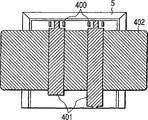
Referring now to Fig. 7,8,9 and 10,, provide following description to the method for a plurality of semiconductor laser installing on the silicon semiconductor substrate.In Fig. 7, affix figure 400 is appended on the silicon chip 1 according to the present invention.Label 401 expression solder flux figures weld semiconductor laser thereon.Electrode pattern 402 is formed and is connected on the solder flux figure 401.On the other hand, Fig. 8 explanation solder flux figure 501 that on the rear side of corresponding semiconductor laser instrument 4a and 4b, forms and affix figure figure that is used to calibrate.Fig. 9 illustrates a kind of method, is used for calibrating being formed at the affix figure 400 on the substrate 1 and being formed between the affix figure 502 on the rear side of semiconductor laser 4a and 4b.In Fig. 9, substrate 1 and semiconductor laser 4a and 4b receive with microscope 601 then with infrared light 600 irradiation from its face side or dorsal part, its reflection or transmitted light beam, and the affix figure is exaggerated and projects on the video monitor 602.In addition, calculate the center of affix figures 400 and 502 by computing machine 603, and mobile substrate 1 or semiconductor laser lentamente, become till zero until the position deviation between two centers.Finish after the aligning, contact joint, weld at a soft heat soldering furnace subsequently.
Figure 10 is a sectional view, and a kind of state is described, wherein semiconductor laser 4a and 4b have been welded on the substrate 1 of catoptron, and it is equivalent to the cross section of A-A ' line intercepting in Fig. 3 A.At the rear side of semiconductor laser, the affix figure 502 that forms electrode 701 and be used to aim at welds semiconductor laser having on electrode 701 and solder flux 702 substrate 1 formed thereon.Between affix figure 502 and 703, carry out aiming at of semiconductor laser and substrate.Light beam from semiconductor laser 4a or 4b forms luminous point 704, and mirror 5 reflections that are reflected, and passes through beam splitter and object lens then, arrives CD.For the light beam from luminous point 704 can not blocked by the substrate bottom, just on substrate, form a pedestal 705.
Figure 11 illustrates an example, and wherein, in order to improve heat radiation, just in time arrangement one deck has the material 800 of high-termal conductivity below semiconductor laser.The heat that produces in the active layer of each semiconductor laser is just in time in its down diffusion, makes heat conduction betide the area of broad, to be reduced to the thermal resistance of heating radiator.Material layer 800 can have a kind of function that discharges stress, and the thermal expansion coefficient difference between semiconductor laser and substrate can be induced this stress.
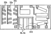
Figure 12 illustrates an example, wherein, settles three semiconductor lasers according to the present invention in the multi-wavelength assembly.These laser instruments begin to be followed successively by from right-hand side: 810, one of the bluish purple semiconductor lasers of the 410nm wavelength of having an appointment the have an appointment red laser 306 of 660nm wavelength and the infrared laser 307 of the 780nm wavelength of having an appointment.For tracking forms three groups of corresponding photoelectric detectors 304,303 and 811, as an example, one group of photoelectric detector is used for following the tracks of and reproducing signal.These three kinds of wavelength relate to recording/reproducing optical disk, comprise super DVD, DVD and CD, and they all are standardized.
Figure 13 illustrates that is further implemented an integrated package of the present invention.On silicon or GaN substrate 102, integrally form an amplifier 900 that is used to amplify the photocurrent that provides from photoelectric detector 303,304 and 302, make the decreased number of used unit, thereby might improve its degree of integration.
According to the present invention, as mentioned above, might realize optical head integrated that reduces and be loaded with a plurality of semiconductor lasers of size, thereby might reach the size of overall optical disc apparatus and reducing of thickness, this equipment is used for the record and the reproduction of for example CD, DVD and CD that can the shallow blue violet lasers of carrier band.