CN112654899A - Apparatus and method for storing wave signals in a cavity - Google Patents
Apparatus and method for storing wave signals in a cavity Download PDFInfo
- Publication number
- CN112654899A CN112654899A CN201980051096.5A CN201980051096A CN112654899A CN 112654899 A CN112654899 A CN 112654899A CN 201980051096 A CN201980051096 A CN 201980051096A CN 112654899 A CN112654899 A CN 112654899A
- Authority
- CN
- China
- Prior art keywords
- cavity
- electromagnetic wave
- wave signal
- signal
- electromagnetic
- Prior art date
- Legal status (The legal status is an assumption and is not a legal conclusion. Google has not performed a legal analysis and makes no representation as to the accuracy of the status listed.)
- Pending
Links
Images


Classifications
-
- G—PHYSICS
- G11—INFORMATION STORAGE
- G11B—INFORMATION STORAGE BASED ON RELATIVE MOVEMENT BETWEEN RECORD CARRIER AND TRANSDUCER
- G11B7/00—Recording or reproducing by optical means, e.g. recording using a thermal beam of optical radiation by modifying optical properties or the physical structure, reproducing using an optical beam at lower power by sensing optical properties; Record carriers therefor
- G11B7/004—Recording, reproducing or erasing methods; Read, write or erase circuits therefor
- G11B7/0045—Recording
-
- G—PHYSICS
- G02—OPTICS
- G02B—OPTICAL ELEMENTS, SYSTEMS OR APPARATUS
- G02B5/00—Optical elements other than lenses
- G02B5/08—Mirrors
- G02B5/0816—Multilayer mirrors, i.e. having two or more reflecting layers
-
- G—PHYSICS
- G02—OPTICS
- G02B—OPTICAL ELEMENTS, SYSTEMS OR APPARATUS
- G02B5/00—Optical elements other than lenses
- G02B5/08—Mirrors
-
- G—PHYSICS
- G02—OPTICS
- G02B—OPTICAL ELEMENTS, SYSTEMS OR APPARATUS
- G02B5/00—Optical elements other than lenses
- G02B5/08—Mirrors
- G02B5/09—Multifaceted or polygonal mirrors, e.g. polygonal scanning mirrors; Fresnel mirrors
-
- G—PHYSICS
- G11—INFORMATION STORAGE
- G11C—STATIC STORES
- G11C13/00—Digital stores characterised by the use of storage elements not covered by groups G11C11/00, G11C23/00, or G11C25/00
- G11C13/04—Digital stores characterised by the use of storage elements not covered by groups G11C11/00, G11C23/00, or G11C25/00 using optical elements ; using other beam accessed elements, e.g. electron or ion beam
- G11C13/042—Digital stores characterised by the use of storage elements not covered by groups G11C11/00, G11C23/00, or G11C25/00 using optical elements ; using other beam accessed elements, e.g. electron or ion beam using information stored in the form of interference pattern
Abstract
The invention discloses an apparatus comprising a cavity comprising a plurality of inner surfaces or reflective elements; one or more transmitters configured to receive the electrical signals, convert the electrical signals to electromagnetic wave signals, and introduce the electromagnetic wave signals into the interior of the cavity; and one or more receivers configured to extract the electromagnetic wave signals, convert the electromagnetic wave signals into corresponding electrical signals, and transmit the corresponding electrical signals to outside of the cavity. Electromagnetic wave signals are confined inside the cavity by undergoing a series of reflections or back and forth propagation between internal surfaces of the cavity or between reflective elements or within the cavity. The apparatus further includes one or more regenerators configured to reamplify, reshape and/or retime the electromagnetic wave signal propagating in the interior of the cavity.
Description
Cross Reference to Related Applications
This non-provisional patent application claims the benefit and priority of U.S. provisional patent application 62/713,735 filed 2018, 8, month 2, the entire contents of which are incorporated herein by reference.
Technical Field
The present invention relates to the field of information storage technology, and in particular to an apparatus and method for storing information in a cavity as a wave signal.
Background
The development of data centers, broadband communications, and computationally intensive signal processing has fueled the need for high capacity data storage with lower power consumption. Furthermore, modern data centers typically require fast access to the same data stored on the same common drive to perform, for example, High Performance Computing (HPC). Additionally, many participants in the Information Technology (IT) storage industry (e.g., end customers, data centers, programmers at systems programming (ISP), programmers at circuits programming (ICP), etc.) are increasingly interested in being able to immediately, definitively, and completely erase sensitive data (e.g., government data, military data).
Currently, example storage devices for storing data in a data center are solid state memory (SSD, e.g., non-volatile NAND flash based memory) and Hard Disk Drive (HDD). Conventional data centers based on solid state storage devices have various disadvantages. For example, data storage using the above-described conventional storage device consumes a large amount of power and requires expensive maintenance. Furthermore, data storage involving many conventional storage devices generates a large amount of heat, and therefore requires a cooling system, which in turn requires additional cost and energy consumption. In addition, the processing capability of reading or writing data of the above conventional electromagnetic wave storage device is, for example, several Gb/s, which is limited by the speed of the electronic device. Furthermore, when erasing data from a conventional non-volatile solid-state memory, it is common to leave an imprint of the erased data, and the erased data can be extracted by suitable technical means. Further, when extending a data center using these conventional storage devices, more storage devices need to be purchased, or the current storage devices need to be replaced with better performing storage devices. Therefore, building and upgrading a data center using conventional storage devices is costly and time consuming.
Accordingly, there is a need for a data storage device and method that overcomes one or more of the above and other deficiencies of data storage using conventional storage devices.
Disclosure of Invention
It has now been found that the above and related objects of the present invention are achieved by several related aspects, including an apparatus and method for storing wave signals (e.g., moving data) within a cavity.
More particularly, the present invention relates to an apparatus comprising a cavity comprising a plurality of inner surfaces or reflective elements; one or more transmitters configured to receive electrical signals, convert the electrical signals to electromagnetic wave signals, and introduce the electromagnetic wave signals into the interior of the cavity; and one or more receivers configured to extract the electromagnetic wave signals, convert the electromagnetic wave signals into corresponding electrical signals, and transmit the corresponding electrical signals to an exterior of the cavity, wherein the electromagnetic wave signals are confined to the interior of the cavity by undergoing a series of reflections or back and forth propagation between multiple interior surfaces or reflective elements of the cavity or within the cavity.
In at least one embodiment, the apparatus further comprises one or more regenerators configured to re-amplify, re-shape and/or re-time the electromagnetic wave signals propagating inside the cavity. In at least one embodiment, the regenerator may comprise an all-optical regenerator or an opto-electrical regenerator.
In at least one embodiment, the cavity interior is configured to enable an atmospheric pressure level different from an atmospheric pressure level outside the cavity. In at least one embodiment, the cavity interior is configured such that the atmospheric pressure level is lower than the atmospheric pressure level outside the cavity.
In at least one embodiment, the apparatus further comprises a vacuum pump configured to maintain the interior of the cavity substantially under vacuum conditions.
In at least one embodiment, the electromagnetic wave signal comprises a modulated laser beam.
In at least one embodiment, the electromagnetic wave signal includes any beam shape. In at least one embodiment, the electromagnetic wave signal comprises a Gaussian beam. In at least one embodiment, the electromagnetic wave signal comprises a non-Gaussian beam.
In at least one embodiment, the electromagnetic wave signal includes a spatial mode. In at least one embodiment, the electromagnetic wave signal includes an Orbital Angular Momentum (OAM) mode.
In at least one embodiment, the cavity is substantially sealed.
In at least one embodiment, the cavity comprises a cubic cavity, a rectangular cavity, a tubular cavity, a torus cavity, a spherical cavity, a polyhedral cavity, a parallelogram cavity, a prismatic cavity, or an ovoid cavity.
In at least one embodiment, the cavity includes a resonant cavity configured to resonate at one or more frequencies of the electromagnetic wave signal.
In at least one embodiment, the one or more transmitters include at least one laser and at least one modulator.
In at least one embodiment, the one or more emitters include at least one directly tuned laser.
In at least one embodiment, the one or more receivers comprise at least one photodetector.
In at least one embodiment, at least one of the one or more transmitters and at least one of the one or more receivers are co-located in the transceiver.
In at least one embodiment, the inner surface of the cavity is at least partially made of a mirror, reflective coating, grating, or photonic micro-structured material configured to reflect or regenerate or separate or process an incident electromagnetic wave signal.
In at least one embodiment, one or more regenerators comprise a crystal or an optical fiber.
In at least one embodiment, the crystal or fiber is doped. In at least one embodiment, the crystal or fiber is doped with a phosphor element.
In at least one embodiment, the one or more regenerators include at least one amplifier and at least one absorber.
In at least one embodiment, the one or more regenerators include at least one amplifier configured to operate in saturation.
In at least one embodiment, one or more regenerators include a non-linear filter.
In at least one embodiment, the one or more regenerators include an all-optical regenerator or an opto-electronic regenerator.
In at least one embodiment, the apparatus further comprises at least one of a lens, a grating, a metamaterial, and an optical material configured to refocus or reshape the electromagnetic wave signal propagating inside the cavity.
In at least one embodiment, the reflective element comprises a plurality of first parallel plates located inside the cavity, wherein at least a portion of each side of each first parallel plate comprises a reflective surface or a surface on which the reflective element is disposed. In at least one embodiment, the first parallel plates are disposed substantially equidistant from each other.
In at least one embodiment, the reflective element further comprises a plurality of second parallel plates disposed perpendicular to the first parallel plates and a plurality of third parallel plates disposed perpendicular to the first and second parallel plates such that the first, second and third parallel plates define a plurality of sub-cavities inside the cavity, wherein at least a portion of each side of each of the second and third parallel plates comprises a reflective surface or a surface on which the reflective element is disposed, and the electromagnetic wave signal is confined inside at least one of the sub-cavities until extracted. In at least one embodiment, the second parallel plates are disposed substantially equidistant from each other. In at least one embodiment, the third parallel plates are disposed substantially equidistant from each other.
In at least one embodiment, the apparatus further comprises a signal focusing device disposed on or adjacent to one or more interior surfaces or reflective elements of the cavity and configured to separate two adjacent overlapping electromagnetic beams and focus them to separate points on the reflective interior surfaces or reflective elements.
In at least one embodiment, the signal focusing means comprises a graded index material, a photonic crystal structure, a mirror structure or a diffractive structure.
In at least one embodiment, the cavity comprises a cubic cavity and the portions of the inner surfaces of the two opposing sides of the cubic cavity comprise a plurality of mirrors configured to reflect an incident electromagnetic wave signal such that the electromagnetic wave signal propagates in a meandering manner in a first plane substantially perpendicular to the two opposing sides of the cubic cavity.
In at least one embodiment, each of the above-described mirrors is configured at an angle α ═ sin-1(s/√(c2+s2) Is used to reflect an incident electromagnetic wave signal, where c is the side length of the cubic cavity and s is the transverse spot size of the electromagnetic wave signal.
In at least one embodiment, the apparatus further comprises a signal directing element configured to direct the direction of propagation of the electromagnetic wave signal in a second plane substantially parallel to and adjacent to the first plane.
In at least one embodiment, the apparatus further comprises a signal directing element configured to direct the direction of propagation of the electromagnetic wave signal in a second plane, the second plane being substantially perpendicular to the first plane.
Furthermore, the present invention relates to a method of using an electromagnetic wave storage device comprising a cavity having an inner surface or a reflective element, one or more transmitters, and one or more receivers, the method comprising the steps of receiving an electrical signal by the one or more transmitters; converting, by one or more transmitters, the received electrical signals into electromagnetic wave signals; introducing an electromagnetic wave signal into the interior of the cavity by one or more emitters, wherein the electromagnetic wave signal is confined within the cavity by undergoing a series of reflections or propagating back and forth between the interior surfaces or reflective elements of the cavity; extracting, by one or more receivers, the electromagnetic wave signal; converting, by one or more receivers, the extracted electromagnetic wave signals into corresponding electrical signals; and transmitting the respective electrical signals from the one or more receivers to outside the cavity.
In at least one embodiment, the electromagnetic wave storage device further comprises one or more regenerators, and the method further comprises re-amplifying, re-shaping and/or re-timing, by the one or more regenerators, the electromagnetic wave signals propagating inside the cavity.
In at least one embodiment, the method further comprises causing the atmospheric pressure level inside the cavity to be different from the atmospheric pressure level outside the cavity. In at least one embodiment, the method further comprises reducing the atmospheric pressure level inside the cavity to a level below the atmospheric pressure level outside the cavity.
In at least one embodiment, the method further comprises maintaining the interior of the cavity substantially under vacuum conditions.
In at least one embodiment, the step of converting, by the one or more transmitters, the received data into an electromagnetic wave signal comprises converting, by the one or more transmitters, the received data into a modulated laser beam.
In at least one embodiment, the step of converting, by the one or more transmitters, the received data into electromagnetic wave signals includes converting, by the one or more transmitters, the received data into a gaussian beam, a non-gaussian beam, or any other beam shape.
In at least one embodiment, the step of converting, by the one or more transmitters, the received data into electromagnetic wave signals comprises converting, by the one or more transmitters, the received data into a spatial pattern. In at least one embodiment, the step of converting, by the one or more transmitters, the received data into electromagnetic wave signals includes converting, by the one or more transmitters, the received data into Orbital Angular Momentum (OAM) mode.
In at least one embodiment, the method further comprises refocusing or reshaping the electromagnetic wave signal propagating inside the cavity by using at least one of a lens, a grating, an optical material, and a metamaterial.
In at least one embodiment, the electromagnetic wave storage device further comprises a signal focusing device disposed on or adjacent to one or more interior surfaces or reflective elements of the cavity and configured to separate two adjacent overlapping electromagnetic beams and focus them to separate points on the reflective interior surfaces or reflective elements, and the method further comprises the steps of focusing the incident electromagnetic wave signals by using the signal focusing device and redirecting the electromagnetic wave signals to opposite directions by using the signal focusing device.
In at least one embodiment, the signal focusing means comprises a graded index material, a photonic crystal structure, a mirror structure or a diffractive structure.
In at least one embodiment, the cavity comprises a cubic cavity and portions of the interior surfaces of two opposing sides of the cubic cavity comprise a plurality of mirrors, and the method further comprises reflecting the incident electromagnetic wave signal by the plurality of mirrors such that the electromagnetic wave signal propagates in a meandering manner in a first plane substantially perpendicular to the two opposing sides of the cubic cavity.
In at least one embodiment, the step of reflecting the incident electromagnetic wave signal by a plurality of mirrors comprises reflecting the incident electromagnetic wave signal by each mirror at an angle α sin-1(s/√(c2+s2) ) is reflected, where c is the side length of the cubic cavity and s is the transverse spot size of the electromagnetic wave signal.
In at least one embodiment, the electromagnetic wave storage device further comprises a signal direction element, and the method further comprises directing, by the signal direction element, a direction of propagation of the electromagnetic wave signal in a second plane that is substantially parallel to and adjacent to the first plane.
In at least one embodiment, the electromagnetic wave storage device further comprises a signal directing element, and the method further comprises directing, by the signal directing element, the electromagnetic wave signal to propagate in a second plane, the second plane being substantially perpendicular to the first plane.
In at least one embodiment, the one or more regenerators comprise an all-optical regenerator, and the steps of re-amplifying, re-shaping, and/or re-timing the electromagnetic wave signal are performed in the optical domain by the all-optical regenerator.
In at least one embodiment, the one or more regenerators comprise an electro-optical regenerator, and the step of re-amplifying, re-shaping and/or re-timing the electromagnetic wave signals comprises the steps of converting the electromagnetic wave signals into corresponding electrical signals by the electro-optical regenerator, re-amplifying, re-shaping and/or re-timing the corresponding electrical signals by the electro-optical regenerator, and converting the regenerated electrical signals into corresponding electromagnetic wave signals in the optical domain by the electro-optical regenerator.
Although specific features, capabilities, and advantages have been enumerated above, various embodiments may include some, all, or none of the enumerated features, functions, and advantages. The above-described and other features, functions, and advantages of the disclosed subject matter, as well as the invention itself, will be more fully understood after a review of the following figures, detailed description, and claims.
Drawings
Exemplary embodiments of the invention will be described below with reference to the accompanying drawings, in which:
FIG. 1 is a schematic diagram of an exemplary embodiment of the present invention using a cubic cavity.
Fig. 2 is a schematic diagram of an optical processing unit according to an exemplary embodiment of the present invention, in which components thereof and interconnections between the components are schematically illustrated.
FIG. 3 is a schematic diagram of a regenerator and its operation according to an exemplary embodiment of the present invention.
FIG. 4A is a cross-sectional view of the interior surfaces of two opposing sides of the cubic cavity of FIG. 1, illustrating electromagnetic beams reflected or propagating back and forth between the interior surfaces according to an exemplary embodiment of the present invention.
Fig. 4B shows a signal directing element according to an exemplary embodiment of the present invention.
FIG. 4C is a cross-sectional view of the interior surfaces of two opposing sides of the cubic cavity of FIG. 1, illustrating electromagnetic beams reflected or propagating back and forth between the interior surfaces according to an exemplary embodiment of the present invention.
FIG. 4D is a cross-sectional view of a signal focusing device made of a gradient index material separating two overlapping electromagnetic beams according to an exemplary embodiment of the present invention.
FIG. 4E is a cross-sectional view of an interior surface including signal focusing devices disposed on two opposing sides of the cubic cavity of FIG. 1, showing electromagnetic beams reflected or propagating back and forth between the signal focusing devices according to an exemplary embodiment of the present invention.
FIG. 4F is a cross-sectional view of the interior surfaces of two opposing sides of the cubic cavity of FIG. 1, illustrating electromagnetic beams reflected or propagating back and forth between the interior surfaces according to an exemplary embodiment of the present invention.
FIG. 4G is a cross-sectional view of a cavity comprising a plurality of parallel plates according to an exemplary embodiment of the invention.
Fig. 5 shows the Rayleigh (Rayleigh) range of the collimated electromagnetic beam.
Fig. 6 shows a gaussian beam propagating in the rayleigh range centered at its focal point.
Fig. 7A is an isometric view of a rectangular cavity according to an exemplary embodiment of the invention.
Fig. 7B is an isometric view of a rectangular cavity according to another exemplary embodiment of the invention.
FIG. 8 is a cross-sectional view of a lumen bottom showing a square area of the tube bottom for volume calculations according to an exemplary embodiment of the present invention.
Figure 9 is a cross-sectional view of an oval cavity illustrating an electromagnetic wave signal traveling between the inner surfaces of the cavity in accordance with an exemplary embodiment of the present invention.
Detailed Description
Information or any kind of data may be stored as electromagnetic waves (e.g., lasers, beams, Radio Frequency (RF) signals, other types of electromagnetic wave signals, to name a few) that may be transmitted and/or reflected between or within structures in various transmission media (e.g., free space, vacuum, crystals, nonlinear media, optical waveguides, optical fibers, etc.). The terms "electromagnetic wave signal" and "electromagnetic beam" are used interchangeably herein. Electromagnetic radiation or beam, as used herein, may include any kind of electromagnetic signal, including a laser beam or signal, a microwave laser beam or signal, a beam or signal, or any type of wired or wireless signal (including acoustic, radio wave, infrared, ultraviolet, microwave band transmission), or any combination of one or more of the foregoing. Although sometimes referred to herein simply as laser beams or signals, other types of optical signals and other types of electromagnetic radiation transmissions (including combinations of wavelength bandwidths of radio waves, microwaves, infrared, ultraviolet, and electromagnetic radiation), whether directed, shaped, phased, or unguided, unshaped, unphased, are also included.
The recirculation loop can be used to store "data in motion" by keeping the electromagnetic wave signal carrying the data constantly reflected or propagating back and forth, transmitted and/or reflected between and/or within structures, and regenerated as needed (e.g., by signal amplification or regeneration). A recirculation loop may be constructed, for example, from a satellite or other spacecraft that reflects or otherwise retransmits data in free space or through a waveguide (e.g., one or more optical fibers). The circulation loop may also comprise a waveguide, such as an optical fiber. Various systems and methods for storing moving data in a circulation loop are described in U.S. patent application No. 15/465,356, which is disclosed as U.S. patent application No. 2017/0280211a1 and is incorporated herein by reference in its entirety.
To increase the data storage time and capacity of the above-described system, the electromagnetic wave signal needs to be held or "delayed" in the circulation loop for as long a time as possible. The delay of the electromagnetic signal may also have other applications, for example enabling the use of a shorter coherence length master oscillator in a long range lidar or radar.
The cavity may be configured to provide a circulation loop for storing or confining electromagnetic wave signals (e.g., moving data). Further, the cavity may be configured to provide various surfaces that reflect or redirect electromagnetic wave signals multiple times to accumulate time-of-flight delays. As used herein, the term "cavity" refers to any structure in which an electromagnetic wave signal can propagate that includes at least one partially or fully enclosed space (e.g., a partially open or fully sealed enclosure) of any size or shape. The enclosed space within the cavity may be hollow and such hollow space has a refractive index of about 1 under near vacuum conditions, which allows electromagnetic wave signals to propagate in the vacuum at speeds close to the speed of light. Alternatively, the enclosed space within the cavity may be filled with a material (e.g., solid, crystalline, amorphous material, liquid, etc.) having a refractive index greater than 1, wherein the propagation of the electromagnetic wave signal is slower than in a vacuum. In another example, the cavity may be a solid material (e.g., crystalline, amorphous solid, to name a few) enclosed by its own inner and outer surfaces. Preferably, such a material filling the cavity is configured to allow storing or confining electromagnetic wave signals with low loss.
As described further below, exemplary geometries for the cavities include cubic cavities, rectangular cavities, tubular cavities, torus cavities, spherical cavities, polyhedral cavities, parallelogram cavities, prismatic cavities, ovoid cavities, and the like (to name a few). In other words, the geometry of the cavity may be configured to fit any available space in any structure, building, or device to construct a data center or any type of customer data computing and/or storage facility or device, to name a few. For example, containers, closets, rooms in a building, interior spaces of a multi-story building, or closed football stadium may all be cavities that provide a circulation loop to store data while in motion. In embodiments, the cavity may comprise an optical resonant cavity that resonates at one or more frequencies of the electromagnetic wave signal.
Electromagnetic wave signals may be confined inside the cavity by, for example, undergoing a series of reflections or propagating back and forth between the inner surfaces of the cavity and/or between reflective elements placed within the cavity. In embodiments, the electromagnetic wave signal may be any type of electromagnetic beam and any combination of different electromagnetic beams. In embodiments, the electromagnetic wave signal may be an electromagnetic wave of any wavelength and may contain any number of different wavelengths. In embodiments, the electromagnetic wave signal may be any spatial pattern and may contain any number of different spatial patterns. For example, the electromagnetic wave signal to be confined inside the cavity may include a modulated laser beam, other types of modulated electromagnetic beams, a gaussian beam, electromagnetic beams of various spatial modes (e.g., circular mode, square mode, Orbital Angular Mode (OAM)), hermitian gaussian or laguerre gaussian, to name a few.
Within a given interior space provided by the cavity, the interior surfaces of the cavity and/or the reflective elements within the cavity may be configured to increase the path length and storage time of electromagnetic wave signals propagating within the cavity. The path length of an electromagnetic wave signal refers to the distance the electromagnetic wave signal travels within the cavity, and the storage time refers to the path length of the electromagnetic wave signal divided by the speed of light or other electromagnetic wave signal (e.g., sound) carrying the moving data within the cavity. As storage times increase and path lengths increase, more in-motion data can be stored in the cavity without requiring higher data rates to introduce the data into the cavity. Thus, if the electromagnetic wave signal carrying the moving data is an acoustic wave, the much lower speed of sound (compared to the speed of light) enables one to store a larger amount of moving data in the cavity without the need for a higher data rate when introducing data into the cavity.
According to an exemplary embodiment, the means for storing an electromagnetic wave signal (e.g., data in motion) may comprise a cavity of any shape, or size. The cavity may be partially closed with one or more openings between the interior space and the exterior of the cavity. Alternatively, the cavity may be completely closed and substantially sealed, with no opening between the interior and exterior of the cavity.
To confine the electromagnetic wave signal, the cavity may include an inner surface or reflective element placed within the cavity that creates a circulation loop for the propagation of the electromagnetic wave signal until extraction from the cavity. All or only a portion of the inner surface of the cavity may be reflective. Some or all of the interior surfaces of the cavity may include any kind of reflective element or material, such as a mirror, reflective coating (to name a few), or grating, or any other photonic microstructure material configured to reflect, reproduce, separate and/or process incident electromagnetic wave signals. In an embodiment, the reflectivity of the inner surface may be as close to 1 as possible, since a high reflectivity of the inner surface will reduce any loss of power and intensity of the electromagnetic wave signal due to reflection.
The exemplary apparatus may also include one or more transmitters and one or more receivers that may be used as input ports to introduce data in the form of modulated electromagnetic wave signals into the cavity interior and as output ports to extract electromagnetic wave signals from the cavity interior, respectively. The transmitter may be configured to receive electrical or electronic signals (e.g., digital data) from outside the cavity or inside the cavity, convert the electrical signals to electromagnetic wave signals, and introduce the electromagnetic wave signals inside the cavity such that the electromagnetic wave signals propagate so as to be confined within the cavity. It should be appreciated that the transmitter may place the electrical or electronic signals on the electromagnetic wave signal using any modulation scheme (e.g., QAM, NRZ, QPSK, etc.) and/or any digital signal processing technique known to those of ordinary skill in the art (e.g., error correction, etc.) necessary to ensure error-free propagation of data within the cavity. The transmitter may include at least one laser and at least one modulator. Alternatively, the transmitter may comprise at least one directly tuned laser. In embodiments, lasers of various wavelengths within the reflective window may be used. The receiver may be configured to extract the electromagnetic wave signal from inside the cavity, convert the electromagnetic wave signal into a corresponding electrical signal (e.g., digital data), and transmit the corresponding electrical signal to outside the cavity. The receiver may comprise at least one photodetector. In an embodiment, the apparatus may comprise one or more transceivers, wherein at least one transmitter and at least one receiver are physically or functionally positioned or combined together.
In embodiments, the means for storing the electromagnetic wave signals (e.g., data in motion) may further comprise one or more amplifiers and/or regenerators configured to restore some or all aspects of the electromagnetic wave signals to their original or previous states. In an embodiment, the apparatus may further comprise one or more devices configured to clean electromagnetic wave signals confined and propagating inside the cavity. Electromagnetic wave signals propagating inside the cavity may suffer from losses in intensity and amplitude, dispersion of the signal, and/or increases in noise and errors due to, for example, multiple reflections off the surface, various chromatic and nonlinear effects, perturbations of the cavity, random scattering events, and/or spontaneous emission of light. Thus, the electromagnetic wave signal may need to be regenerated at different points in time or space as it propagates within the cavity.
In an embodiment, a regenerator may be disposed along the electromagnetic beam path and used to restore the passing electromagnetic wave signal to its original state and/or to compensate for any degradation.
Full signal regeneration is commonly referred to as a "3R" process, which includes retiming, reshaping, and reamplifying (or amplifying) of the signal. The regenerator in the apparatus may be configured to perform all electromagnetic wave signal regeneration. Alternatively, the regenerator in the apparatus may be configured to recover only some aspects of the electromagnetic wave signal by partially retiming and/or reshaping and/or replaying the large electromagnetic wave signal. In an embodiment, the regenerator may also be configured to implement error correction to recover lost information or to correct errors introduced into the moving data. The number of regenerators of the device depends on the design of the chamber and the performance of the chamber elements and can range from zero to very large numbers.
Any device configured to fully or partially re-amplify, re-shape, and/or re-meter the time electromagnetic wave signal may be used to construct the regenerator. The regenerator may be implemented in a variety of ways. In an embodiment, the regenerator may be an all-optical or electro-optical regenerator, wherein the all-optical regenerator is configured to regenerate the electromagnetic wave signal in an all-optical manner in the optical domain, and the electro-optical regenerator is configured to convert the electromagnetic wave signal into a corresponding electrical signal in the electrical domain, to electrically regenerate the converted electrical signal, and to convert the regenerated electrical signal back into a corresponding electromagnetic wave signal in the optical domain. In an embodiment, the regenerator may comprise at least one amplifier and at least one absorber. In an embodiment, the regenerator may include at least one amplifier configured to operate in saturation. In embodiments, the amplifier may be any device configured to amplify an optical signal. In an embodiment, the amplifier may comprise a crystal or an optical fiber. In an embodiment, the crystal and the optical fiber may be doped with a fluorescent element. In an embodiment, the optical fiber used in the amplifier may comprise additional means for injecting the optical signal into the fiber at the input end, and further means for restoring the beam to its original shape and size at the output end. In an embodiment, the regenerator may include a nonlinear filter configured to provide a stable gain and reduce noise in the electromagnetic wave signal. In embodiments, the regenerator may comprise a crystal or an optical fiber. In an embodiment, the regenerator may comprise a doped crystal or an optical fiber. In an embodiment, the crystal or optical element may be doped with a fluorescent element. In an embodiment, the optical fiber used in the regenerator may include additional means at the input end to inject the electromagnetic wave signal into the optical fiber and another means at the output end to restore the electromagnetic beam to its original shape and size.
In an embodiment, an apparatus for storing an electromagnetic wave signal may include a cavity, wherein an interior of the cavity is configured to enable a different (e.g., higher or lower) level of atmospheric pressure than an exterior of the cavity. In an embodiment, the cavity interior may be configured such that the atmospheric pressure level is lower than the atmospheric pressure level outside the cavity. This may be achieved, for example, by a vacuum pump or any other pressure reduction device. In embodiments, the means for storing electromagnetic wave signals may further comprise a vacuum pump and/or other means for creating a "clean room" type environment that may be used to maintain a desired level of vacuum conditions (e.g., a vacuum, or a subatmospheric pressure near a vacuum) inside the cavity. Alternatively, the device may be placed entirely in a vacuum (e.g., an external space) as another way of providing vacuum conditions in the cavity. By maintaining the interior of the cavity substantially under vacuum conditions, the effects of the atmosphere on the electromagnetic wave signal are reduced or eliminated, and the electromagnetic wave signal propagating inside the cavity suffers negligible power loss or data degradation. For example, dust and other small particles can cause diffraction of electromagnetic waves of the electromagnetic wave signal. While under vacuum conditions, dust and other small particles may be eliminated in the substantially sealed cavity. Similarly, vacuum pumps and/or other means for creating a "clean room" type environment may be used to reduce or eliminate dust and other small particles present in the partially sealed cavity. In addition, the heat generated by the propagation of the optical or electromagnetic signal in a vacuum is negligible, thus reducing the need for a cooling system for the device.
According to an exemplary embodiment, a method of storing an electromagnetic wave signal (e.g., data in motion) may include the following processes. Electrical signals (e.g., electronic digital data) from outside the cavity may be received by one or more transmitters that convert the received electrical signals into electromagnetic wave signals. It should be appreciated that the transmitter may place the electrical or electronic signals on the electromagnetic wave signal using any modulation scheme (e.g., QAM, NRZ, QPSK, etc.) and/or any digital signal processing technique known to those of ordinary skill in the art (e.g., error correction, etc.) necessary to ensure error-free propagation of data within the cavity. The transmitter introduces an electromagnetic wave signal into the cavity, which is confined within the cavity by undergoing a series of reflections or propagating back and forth between the inner surfaces of the cavity or reflective elements. Electromagnetic wave signals may be extracted from the interior of the cavity and converted to corresponding electrical signals (e.g., electronic digital data) by one or more receivers. The receiver may then transmit the corresponding electrical signal outside the cavity.
In an embodiment, to compensate for any degradation of the electromagnetic wave signal as it propagates inside the cavity, one or more regenerators may be used to restore the electromagnetic wave signal to its original or previous amplitude or waveform. In an embodiment, to reduce or eliminate the effect of the atmosphere on the electromagnetic wave signal, the atmospheric pressure level inside the cavity may be different from the atmospheric pressure level outside the cavity. For example, the atmospheric pressure level inside the cavity may be lower than the atmospheric pressure level outside the cavity. This step may be performed by, for example, a vacuum pump, other means for creating a "clean room" type environment, and/or any pressure reduction means. In an embodiment, the interior of the cavity may be maintained substantially under vacuum conditions by a vacuum pump.
The data storage capacity of the cavity may depend on the size of the optical path length L, the bandwidth B or wavelength range used, the modulation format used (e.g., bits/symbols and type of signal modulation), and the number of electromagnetic modes (e.g., laser, polarization, or spatial multiplexing) used for the electromagnetic wave signal used per frequency/wavelength M. Depending on the design of the cavity, the electromagnetic wave signal may be any spatial lateral and/or longitudinal shape (e.g., circular, square, orbital angular pattern, to name a few). For example, the total data storage capacity of the cavity can be calculated by the formula M L B/2 x (# bits/symbol)/v, where v is the propagation speed of the electromagnetic wave signal in the cavity. If the cavity is in a vacuum, then the speed of the electromagnetic wave signal will be the speed of light in the vacuum. One can increase the data storage capacity of the cavity by, for example, expanding the bandwidth or mode of the electromagnetic wave signal confined within the cavity (e.g., by using additional forms of multiplexing) without having to increase more floor space and/or replace existing hardware.
In an embodiment, the means for storing electromagnetic wave signals (e.g. data in motion) may also be configured to delete the data in motion stored in the cavity by extinguishing or "turning off" the electromagnetic wave signals confined within the cavity. When the electromagnetic wave signal disappears, the data stored therein is certainly lost immediately and cannot be recovered, unlike the data erased from the solid-state memory.
Referring now to the drawings, and in particular to FIG. 1, there is depicted an exemplary embodiment in the form of an apparatus 100 for storing moving data using a cubic cavity 101. Although the cavity walls may be opaque and not necessarily transparent or translucent, fig. 1 illustrates cubic cavity 101 as having its cavity walls transparent in order to present electromagnetic wave signals 104 propagating back and forth between the cavity interior surfaces inside the cavity. As shown in fig. 1, an electromagnetic wave signal is confined inside the cavity 101 by passing through a series of reflections or propagating back and forth between the inner surfaces of the cavity.
Some or all of the portions of the inner surface of each of the six sides of the cubic cavity 101 may be reflective to allow reflection of incident electromagnetic wave signals. In embodiments, some portions of the inner surface of the cavity may be non-reflective (rather than opaque or transparent) to facilitate the working design of the device. The interior surfaces of the cavity 101 may use any kind of reflective element or material, such as mirrors, reflective coatings (to name a few), or gratings, or any other photonic micro-structured material configured to reflect, reproduce, separate and/or process incident electromagnetic wave signals. The reflectivity of the surface being determined by the reflected light or electromagnetic wave signal (P)r) Is divided by the incident light orElectromagnetic wave signal (P)i) Is defined by and is less than or equal to 1. In an embodiment, the reflectivity of the inner surface of the cubic cavity 101 is as close to 1 as possible.
As shown in fig. 1, an exemplary apparatus 100 for storing electromagnetic wave signals (e.g., data in motion) may include one or more optical processing units (OPUs or "access Point terminals (TAP points)") 102. Each OPU102 may be configured to function as an input/output (I/O) port to receive electrical signals (e.g., digital data) for storage in cavity 101 as electromagnetic wave signals, and to access and extract stored electromagnetic wave signals from cavity 101. The number and location of OPUs for the apparatus is not limited to that shown in fig. 1 and may be arbitrary and flexible to accommodate any number and arrangement of computing units, devices, and/or data centers coupled to the apparatus. In embodiments, one or more OPUs 102 may be located inside cavity 101.
Each OPU102 may include a plurality of functional sub-components, and may contain one or more of a transmitter, a receiver, a regenerator, and other functional sub-components for electronic and/or photonic processing. The general purpose of the transmitter is to write data into cavity 101. To this end, the transmitter may be configured to convert an electrical signal (e.g., digital data) into an electromagnetic wave signal 104 carrying the moving data using, for example, a laser. The transmitter may include a laser and modulator, or a directly tuned laser. The electromagnetic wave signals may use lasers of different wavelengths as long as they are within the reflective window of cavity 101. OPU102 may contain a desired number of emitters. Each transmitter may also contain a desired number of digital and/or photonic sub-components to modulate the electromagnetic wave signal 104 in any complex format and/or to generate any transverse spatial pattern for the beam shape of the electromagnetic wave signal.
The general purpose of the receiver is to read data from the cavity 101. The receiver may include a photodetector configured to convert the electromagnetic wave signal 104 into an electrical signal, such as electronic digital data. OPU102 may contain a desired number of receivers. Each receiver may also contain digital and/or photonic sub-components for error correction or other digital processing purposes.
In an embodiment, OPU102 may also include one or more regenerators configured to regenerate electromagnetic wave signal 104 propagating in cavity 101. The regenerator may be configured to reamplify and/or retime and/or reshape the electromagnetic wave signal. The regenerator may also be configured to perform error correction to recover lost information (e.g., lost data bits) in the electromagnetic wave signal. The regenerator may comprise an all-optical regenerator or an opto-electrical regenerator.
In an embodiment, OPU102 may also be configured to delete in-motion data stored in the cavity by extinguishing or "turning off" the electromagnetic wave signal. When the electromagnetic wave signal disappears, the data stored therein is immediately lost completely and cannot be extracted, unlike the data erased from the solid-state memory.
Fig. 2 provides a schematic diagram of OPU102 according to an exemplary embodiment. As shown, electronic digital data is input to or output from OPU102 through digital bus 201. The digital bus 201 is coupled to one or more transceivers 202. Each transceiver 202 may include at least one transmitter and at least one receiver. In an embodiment, OPU102 may include multiple transceivers corresponding to different wavelengths of electromagnetic wave signals. Any wavelength and any number of different wavelengths may be used. In addition, OPU102 may also include multiple transceivers corresponding to different spatial modes of the electromagnetic wave signal. Any spatial pattern and any number of different spatial patterns may be used.
For example, FIG. 2 shows that OPU102 includes multiple transceivers, each corresponding to each of P different wavelengths and each of M different spatial modes, i.e., a total of P M transceivers (transceiver 202-1-1 for λ M)1And spatial mode 1, …, Transceiver 202-P-1 for λPAnd spatial mode 1, …, Transceiver 202-1-M, for λ1And spatial mode M … transceiver 202-P-M for λPAnd spatial mode M). Each of transceivers 202-1-x through transceivers 202-P-x may be configured to convert digital data received over digital bus 201 to have a corresponding wavelength λ1…λP. It should be understood that each transceiverThe electrical or electronic signals may be placed on the electromagnetic wave signals using any modulation scheme (e.g., QAM, NRZ, QPSK, etc.) and/or any digital signal processing technique known to those of ordinary skill in the art (e.g., error correction, etc.) necessary to ensure error-free propagation of data within the cavity.
In an embodiment, OPU102 may also include one or more wavelength division multiplexers/demultiplexers. For example, FIG. 2 shows that OPU102 includes a plurality of wavelength division multiplexers/demultiplexers 203-1 … 203-M, each corresponding to one of M different spatial modes of an electromagnetic wave signal. Each wavelength division multiplexer 203 may be configured to combine different electromagnetic beams of different wavelengths into a single electromagnetic beam, while each wavelength division demultiplexer 203 may be configured to reverse the function of separating an electromagnetic beam containing many wavelengths into electromagnetic beams of different wavelengths. Each wavelength division multiplexer/demultiplexer may be implemented using a set of filters, prisms, resonators, and/or gratings configured to redirect an electromagnetic beam based on its wavelength.
As shown in fig. 2, electromagnetic beams having P different wavelengths from transceivers 202-1-x to 202-P-x may be combined by wavelength division multiplexer 203-x into a single electromagnetic beam, which may be further processed by beamformer 204-x corresponding to spatial mode x. For example, the OPU102 may include M beamformers 204-1 … 204-M corresponding to M different transverse spatial modes, as shown in FIG. 2. Each beamformer 204 may be configured to convert an incident electromagnetic beam into an electromagnetic beam having a particular beam profile (e.g., a particular transverse spatial mode). These beamformers may produce any spatial pattern and any number of different spatial patterns. In an embodiment, the beamformer 204 may include a liquid crystal-based spatial light modulator that may be reprogrammed. Alternatively, the beamformer 204 may include a phase mask having reflective or transparent surfaces that may modify the phase of the electromagnetic beam relative to its lateral spatial position.
In an embodiment, OPU102 may further include a spatial mode multiplexer/demultiplexer 205. The spatial mode multiplexer 205 may be configured to combine electromagnetic beams of different beam profiles (e.g., having different transverse spatial modes) into a single beam containing all incident beam profiles (e.g., transverse spatial modes). On the other hand, the spatial mode demultiplexer 205 may be configured to perform the reverse function, i.e. to separate an electromagnetic beam containing a number of beam profiles (e.g. transverse spatial modes) into electromagnetic beams having different beam profiles (e.g. transverse spatial modes). In an embodiment, the spatial mode multiplexer may comprise a coupler or combiner, which may be implemented by a combination of combining two incident electromagnetic beams into one beam splitter. In an embodiment, the spatial mode demultiplexer may comprise a beam splitter used in another direction such that the incident electromagnetic beam is propagated into a different path. On each path, a spatial filter comprising a spatial light modulator or phase mask may be used, which is configured to separate different beam profiles (e.g. transverse spatial modes).
As shown in FIG. 2, electromagnetic wave signals from the beamformer 204-1 … 204-M having M different transverse spatial modes may be combined by the spatial mode multiplexer 205 into a single electromagnetic wave signal, which now contains P different wavelengths and M different spatial modes. The single electromagnetic wave signal may be sent to a switch 206 that may be controlled by a controller interface 209. When the switch 206 is turned on, electromagnetic wave signals generated based on received electrical signals (e.g., digital data) and processed by the OPU102 to include P different wavelengths and M different spatial modes are introduced into the interior of the cavity 101 through, for example, an optical circulator 207. An optical circulator is a multi-port optical device configured such that an electromagnetic beam entering any port is emitted from the next port.
In an embodiment, OPU102 may include one or more regenerators 208. For example, an electromagnetic wave signal contained in the cavity 101 may be extracted from the inside of the cavity through the circulator 207 and sent to the regenerator 208 for full or partial regeneration. The regenerated electromagnetic wave signal from the regenerator 208 may then be sent to the switch 206 so that the regenerated electromagnetic wave signal may be reintroduced into the interior of the cavity 101 through the optical circulator 207, as shown in fig. 2.
In an embodiment, the OPU102 shown in fig. 2 may also allow reading or extraction of electromagnetic wave signals stored in the cavity 101 (e.g., electromagnetic wave signals carrying moving data) that may be extracted from the cavity 101 through the circulator 207, regenerated by the regenerator 208, and sent to the single 2 x 2 switch 206. Alternatively, two 1 × 2 optical switches may be used instead of the single switch 206. The electromagnetic wave signals may then be demultiplexed by the spatial mode demultiplexer 205 and the wavelength demultiplexer 203 into electromagnetic beams having different transverse spatial modes and different wavelengths, respectively. The transceiver 202 may then convert the electromagnetic wave signals back into corresponding electrical signals in the electronic domain and send the corresponding electrical signals out of the cavity over the digital bus 201.
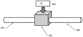
In an embodiment, one or more regenerators separate from any OPU102 may be placed inside cavity 101 along the optical path. For example, FIG. 3 illustrates the operation of an exemplary regenerator 301 placed inside a cavity. Regenerator 301 may comprise an amorphous solid material or a crystalline stack having compensating properties. Preferably, the regenerator 301 is configured to re-amplify, re-shape and/or re-time the electromagnetic wave signal beam (e.g., the incoming weak electromagnetic wave signal beam 303) into a regenerated electromagnetic wave signal beam 304 without changing its shape and/or adding noise to the electromagnetic wave signal. Preferably, the regenerator 301 is configured to allow efficient energy transfer from the pump 302 to the electromagnetic wave signal 304. In an embodiment, the pumping of the crystal in the regenerator 301 may be performed electrically or by an optical laser attached to the crystal. The crystal of regenerator 301 may be highly nonlinear or eventually doped with a fluorescent element. In an embodiment, the regenerator 301 may be an all-optical regenerator or an opto-electronic regenerator.
OPU102 shown in fig. 2 may be used not only for cubic cavities, such as cubic cavity 101 shown in fig. 1, but also for cavities of any size or shape, including rectangular cavities (as shown in fig. 7A-7B), lumens (such as lumen 801 shown in fig. 8), ovoid cavities (such as ovoid cavity 901 in fig. 9), and resonant cavities, to name a few.
Returning to fig. 1, according to an exemplary embodiment, an exemplary apparatus 100 for storing electromagnetic wave signals may optionally include a vacuum pump 105. A vacuum pump 105 may be used to ensure that a desired level of vacuum conditions are maintained inside the cavity 101. The vacuum may be used to maintain a desired quality or intensity of the electromagnetic wave signal beam 104 by reducing or eliminating atmospheric distortion or dust particles within the cavity 101.
Referring now to FIG. 4A, a cross-sectional view of the inner surface 402 of two opposing sides of the cubic cavity 101 is depicted, showing an electromagnetic beam 401 propagating back and forth between the inner surfaces, according to an exemplary embodiment of the present invention. The electromagnetic beam 401 has a transverse spot size s (or diameter if the electromagnetic beam is circular). The spot of the electromagnetic beam may be of any shape depending on the transverse spatial pattern or beam shape of the electromagnetic beam 401.
As shown in fig. 4A, the OPU102 or emitter of the apparatus 100 may be configured such that the electromagnetic beam 401 enters the interior of the cavity 101 from a corner 403 of the cube parallel to the upper side of the cavity. However, the location and manner in which the electromagnetic beam enters the cavity is not a limitation of the present invention, and the electromagnetic beam may enter the cavity in any manner from any location on the cavity wall.
On each of two opposite sides of the cubic cavity 101, a set of tilted mirrors 402 may be placed. Each of these mirrors 402 may be configured to reflect an incident electromagnetic beam to the next mirror located on the opposite side such that the electromagnetic beam 401 propagates in a meandering manner between the inner surfaces of the two opposite sides of the cubic cavity 101, as shown in fig. 4A.
In an embodiment, mirror 402 may be further configured to reflect an incident electromagnetic beam to the next mirror located on the opposite side such that electromagnetic beam 401 propagates in a meandering manner in a plane substantially perpendicular to the two opposite sides of cubic cavity 101. For example, each mirror 401 may be inclined at an angle α sin with respect to a respective edge of the cube-1(s/(2√(c2+s2) C) where c is the side length of the cubic cavity 101 and s is the transverse spot size of the electromagnetic beam. As shown in FIG. 4A, an electromagnetic beam 401 passes through the substrateThe mirror 402 on the opposite side of the cube reflects off a face of the cube cavity having a surface area c in a serpentine manner2The thickness is s. In an embodiment, tilting mirror 402 may also include optical power to focus or defocus the incident electromagnetic beam. In an embodiment, the tilting mirror 402 may be configured to refocus the electromagnetic beam to keep it small. In embodiments, instead of tilted mirrors, signal focusing devices, photonic structures, diffractive structures, metamaterials, or other optical elements may be placed at the sides of the cubic cavity to deflect the electromagnetic beam by a desired angle (e.g., angle α).
The cavity 101 may also include signal directing devices or elements configured to direct the propagating electromagnetic beam in different directions. For example, the signal directing element 404 may be placed at a corner diagonally opposite the point 403 where the electromagnetic beam is introduced into the cavity 101, as shown in FIG. 4A. The signal directing element 404 may be configured to direct the electromagnetic wave beam 401 at an angle (e.g., angle α) with respect to a plane perpendicular to the electromagnetic wave beam propagation 401 shown in fig. 4A. For example, the signal direction element 404 may include a mirror that is slightly larger than the electromagnetic beam size and may be placed near an angle and tilted at an angle (e.g., angle α) with respect to the plane of the electromagnetic beam propagation 401. Alternatively, signal-directing element 404 may include other optical elements or materials, such as transparent materials, waveguides, gradient index (GRIN) materials, prisms, or any suitable combination of these elements and materials having refractive indices designed to direct the electromagnetic beam in a desired manner. Although the bandwidth of these optical materials and components may be limited, their limitations may be overcome using appropriate combinations of these materials and components.
The electromagnetic beam may be directed by signal directing element 404 to another signal directing element on the opposite side of the cube, for example, mirror 405 inclined at an angle α relative to a plane parallel to the plane in which the previous electromagnetic beam propagates as shown in FIG. 4B. The signal directing element 405 may be configured to direct the electromagnetic beam at an angle α such that the propagation of the electromagnetic beam becomes parallel to the previously propagated plane shown in FIG. 4A. After being reflected by the signal directing element 405, the electromagnetic beam 401 begins to propagate in a meandering manner in the next plane adjacent and parallel to the previously propagating plane shown in FIG. 4A by being reflected by mirror 402 shown in FIG. 4B.
In an embodiment, cavity 101 may further include additional signal directing elements such that electromagnetic beam 401 may be swept in one direction through the volume of cubic cavity 101 by repeating the above-described reflection process (e.g., reflected in a meandering manner in the x-y plane) and directed to the next stage (e.g., directed in the z-direction by signal directing elements 404, 405).
In an embodiment, the cavity 101 may further comprise an additional signal directing element configured to direct the electromagnetic beam in a direction perpendicular to the previous propagation direction, such that when the volume of the cubic cavity 101 has been swept by the electromagnetic beam in one direction, the signal directing element may be configured to direct the electromagnetic beam to propagate in a plane (e.g., an x-z plane) within the cubic cavity that is perpendicular to the initial propagation plane (e.g., an x-y plane). For example, where the electromagnetic beam has completed scanning the volume of the cubic cavity in one direction, a mirror slightly larger than the size of the electromagnetic beam may be placed to direct the electromagnetic beam at 90 °. For this purpose, the mirror is inclined by 45 ° with respect to the side wall of the cavity, which is parallel to the direction of the incident electromagnetic beam. Alternatively, the signal-directing elements may comprise other optical elements or materials, such as transparent materials, waveguides, gradient index (GRIN) materials, prisms, or any suitable combination of any of these elements and materials, having refractive indices designed to direct the electromagnetic beam in a desired manner. Although the bandwidth of these optical materials and components may be limited, their limitations may be overcome using appropriate combinations of these materials and components.
In an embodiment, the propagation of the electromagnetic beam in a plane perpendicular to the initial plane of propagation of the electromagnetic beam may be achieved by reflection between mirrors placed on two other different sides of the cube, the arrangement of the mirrors being similar to that shown in fig. 4A. When the cubic cavity 101 has been swept a second time (e.g., zigzagged in the x-z plane), additional signal directing elements may be provided within the cavity 101 to direct the electromagnetic beam in a vertical direction such that the electromagnetic beam propagates in a plane (e.g., zigzagged in the y-z plane) that is perpendicular to the two propagation planes (e.g., x-y and x-z planes) previously used by the electromagnetic beam. Thus, the electromagnetic beam may scan the cavity 101 a third time in a direction perpendicular to the first two scans.
In an embodiment, after the electromagnetic beam has swept the cube cavity 101 a third time, additional signal directing elements, such as mirrors disposed perpendicular to the direction of propagation of the electromagnetic beam, may be used to reflect the electromagnetic beam in the opposite direction so that the electromagnetic beam may begin to sweep the volume of the cube cavity 101 a further three times in the opposite direction.
Returning to fig. 4A, assuming that s is less than c, and thus the angle α is small, the electromagnetic beam 401 bounces 2c/s times from the inner surface 402 in each plane in which the electromagnetic beam propagates, and propagates approximately a distance c after each bounce. Thus, the path length of the electromagnetic beam of each plane is 2c2And s. Assuming that all sides of the cubic cavity 101 have the same arrangement of internal surfaces as shown in fig. 4A, the path length of the electromagnetic beam sweeping six times through the cubic cavity volume in three perpendicular directions is L-12 c3/s2。
Depending on the reflectivity of the interior surfaces (e.g., mirrors), amplifiers and/or regenerators may be placed along the electromagnetic beam path to restore the electromagnetic wave signal to its original intensity and shape (e.g., as discussed above in connection with figure 3). Furthermore, by achieving a vacuum condition inside the cavity 101, for example, using the vacuum pump 105, the electromagnetic beam is not absorbed during propagation between the two inner surfaces (e.g., the mirror 402). In this case, the entire spectrum of available lasers can be used to spread the bandwidth and thus the data storage time and capacity of the cavity.
In addition, various optical devices may be used within the cavity to refocus or reshape the electromagnetic beam propagating within the cavity. For example, the construction of such an optical device may use one or more of lenses, gratings, metamaterials, and other optical elements or materials configured to modify the wavefront of the electromagnetic beam.
The beam size of the electromagnetic wave signal may be an important factor in the data storage capacity of the cavity. The beam waist of the electromagnetic beam as a function of the distance R is given by (1):

where λ is the wavelength of the electromagnetic beam, RfIs the Rayleigh (Rayleigh) range.
If a collimated beam is emitted from an aperture, the beam waist and its diameter are in the Rayleigh range R which is the origin of the far field (far field)fOuter extension √ 2 times. Fig. 5 shows how the collimated beam is in the rayleigh range RfThe near field inside remains collimated and begins to diverge at a constant angular beamwidth outside the rayleigh range.
In embodiments, instead of using a curved surface to restore the reflected electromagnetic wave to a collimated wave, a reflective surface may be used to focus the electromagnetic beam between two reflective surfaces. In this case, the electromagnetic beam has the same size on the opposite reflective surfaces, instead of v 2 times larger. For example, fig. 6 shows that the electromagnetic beam size is the same on both sides of the focal point.
The size of the electromagnetic beam can be kept small in order to store a maximum amount of data within the cavity. Furthermore, to avoid excessive power loss, each focusing element is preferably configured to capture a high percentage of the electromagnetic beam. To capture a high percentage of the electromagnetic beam, the diameter D of the optical element (e.g., aperture, lens, mirror, etc.) may be expanded by a factor of 1.5, corresponding to the beam waist w 03 times of (a), as shown in (2):
D=3√(λRf/π), (2)
in an embodiment, a spatial mode, such as an OAM mode, may be used with a gaussian mode to increase data storage capacity. This substantially gaussian beam is the beam of the electromagnetic wave known to have the lowest divergence. If OAM modes are used, the electromagnetic beam size may be set based on the design wavelength, and within the same beam size, many OAM modes may be located within shorter wavelengths. According to an exemplary embodiment of spatial multiplexing, the beam waist of any given range of OAM modes increases with the square root of the absolute value of the OAM mode number L. Thus, equation (2) for beam diameter D can be modified to (3):
D=3√(λRf(√L)/π), (3)
where the diameter of the electromagnetic beam is assumed to be the same at both ends of the link.
In an embodiment, a gaussian mode electromagnetic beam with a specific design wavelength may be used for data storage. At shorter wavelengths, the beam size can be kept constant by using more OAM modes. The shorter the wavelength, the more OAM modes can be used.
In an embodiment, the electromagnetic wave signal may be stored in a cavity having two parallel reflective plates facing each other, the distance between the two parallel reflective plates being in the rayleigh range. For example, data in motion may be stored in a cavity by propagating an electromagnetic beam back and forth in one direction between two reflective plates. When an electromagnetic beam impinges on the counter-panel, its diameter is expanded by √ 2 times. In this case, the far field angle diffraction limit need not be used, since the distance between the two plates is at the transition between the near field and the far field.
Referring now to FIG. 4C, which depicts a cross-sectional view of a cubic cavity 101 according to another exemplary embodiment, the cubic cavity 101 has two tilted continuous mirror plates 431 on two opposite sides of the cavity. To minimize the spot size of the electromagnetic beam when it reaches the reflective element on the inner surface of the cavity, the electromagnetic beam preferably reaches its minimum size halfway between the two opposing cube sidewalls. Furthermore, in order to capture a high percentage (e.g., more than 99%) of the electromagnetic beam at the receiver, the aperture preferably has a diameter of at least s ═ 3 √ (λ c/π), where λ is the wavelength of the electromagnetic beam and c is the side length of the cubic cavity 101.
For a multi-wavelength electromagnetic beam, the transverse spot size of the electromagnetic beam may vary depending on the wavelength of the electromagnetic beam. As shown in FIG. 4C, the electromagnetic beam 432 having a short wavelength has a small spot size, while the electromagnetic beam having a long wavelengthThe electromagnetic beam 433 has a larger spot size. Thus, to ensure that there is no electromagnetic beam overlap, the highest wavelength can be used to calculate the angle α at which the two mirror plates 431 are tilted with respect to the respective sides of the cube. Since a small portion (e.g., less than 1%) of the electromagnetic beam at the highest wavelength may still overlap, the continuous mirror 431 or signal focusing device may be used as an inner surface on the sidewall of the cubic cavity 101, as shown in fig. 4C, in order not to lose those portions of the electromagnetic beam. In practice, the highest wavelength ranges from 1 micron to 20 microns, corresponding to 5 × 10⁻⁴Arc degree to 10-2The angle of the arc. In this case, the upper limit of the optical path length is set to 4c2π/(3 λ) where c is the side length of the cubic cavity and λ is the wavelength of the electromagnetic wave signal.
In an embodiment, the electromagnetic beam within the cavity 101 may be focused to a smaller spot size before and/or after striking the inner surface of the cavity or the reflective element to increase the path length of the electromagnetic beam. This may be achieved, for example, by placing one or more signal focusing devices on or adjacent to the inner surface of the cavity, which are optical devices configured to focus each electromagnetic beam to a small spot size (e.g., as small as a few microns), even though the electromagnetic beams may overlap. In embodiments, the signal focusing device may also be placed on or adjacent to any reflective element anywhere within the cavity. In an embodiment, the signal focusing means may be configured to distinguish and separate two adjacent overlapping electromagnetic beams and focus them to separate points on the inner surface of the cavity or on the reflective element. In an embodiment, the signal focusing device may be used to compensate for any resulting dispersion on the multi-wavelength electromagnetic wave signal.
For example, the signal focusing means may comprise one or more layers of gradient index (GRIN) material. Fig. 4D shows how a signal focusing device 453 made of multiple layers of GRIN material distinguishes and separates overlapping incident 451 and exiting 452 electromagnetic beams and focuses them to separate points on the inner surface 454 of the cavity, according to an exemplary embodiment.
Fig. 4E is a cross-sectional view of an interior surface 443 of the cubic cavity 101 on two opposing sides with a signal focusing device 442 placed on or adjacent to the interior surface, according to an exemplary embodiment. Figure 4E shows that electromagnetic beam 441 is redirected each time it is reflected from inner surface 443 and signal focusing device 442. In this example, the signal focusing device 442 is configured to distinguish two overlapping electromagnetic beams and focus them at different locations on the inner surface 443.
In embodiments, the signal focusing device may be replaced by or used in conjunction with other optical elements, such as mirrors of special geometry configured to focus the beam on either side of the cavity, and/or photonic crystal structures like apertures in the signal focusing device, and/or diffractive structures, to achieve the desired optical effect. For example, Gaussian electromagnetic beams may partially overlap as they fly within the cavity, provided they are distinguished from each other at the recovery point. To separate the electromagnetic beams at the input/output of, for example, a transmitter, receiver or transceiver, a combination of different angle mirrors and/or signal focusing means may be used. FIG. 4F is a cross-sectional view of a cubic cavity 101 according to another exemplary embodiment. On one side of the cubic cavity 101, a combination of signal focusing means 462 and a continuous mirror plate 464 tilted at an angle is placed, while on the opposite side of the cavity 101, a combination of mirrors 463, 465 tilted at different angles are placed. The exemplary embodiment is configured to discretize the overlapping electromagnetic beam 461 into distinct electromagnetic beams at the transceiver.
To increase the data storage capacity of a cavity (e.g., a cubic cavity), a plurality of parallel plates may be placed inside the cavity. Each side of each plate may partially or fully comprise a reflective surface or surfaces on which reflective elements are provided. Each of the reflective surface and the reflective element may comprise any kind of reflective element or material, such as a mirror, reflective coating (to name a few), or a grating, or any other photonic micro-structured material configured to reflect, reproduce, separate and/or process incident electromagnetic wave signals. In an embodiment, as shown in fig. 4G, the parallel plates 471 may be disposed substantially equidistant from each other inside the cubic cavity 101. The plates may be placed in any of three perpendicular directions parallel to the faces of the cube.
In an embodiment, a second set of parallel plates may be further added to the cavity along one of two other perpendicular directions parallel to the cube faces. The second set of parallel plates may be positioned substantially equidistant from each other. In embodiments, a third set of parallel plates may be further added to the cavity, wherein the third set of parallel plates is perpendicular to the first and second sets of parallel plates. The third set of parallel plates may be positioned substantially equidistant from each other. Each side of each of the second and third sets of parallel plates may partially or completely comprise a reflective surface or a surface on which a reflective element is disposed. Each of the reflective surface and the reflective element can comprise any type of reflective element or material, such as a mirror, reflective coating (to name a few), or grating, or any other photonic microstructure material configured to reflect, reproduce, separate, and/or process incident electromagnetic wave signals. The first, second and third sets of parallel plates may together define a plurality of sub-cavities. Some or all of these sub-cavities may be configured to confine electromagnetic wave signals.
Assuming that a set of multiple parallel plates fit throughout the cubic cavity 101 and are arranged equidistantly between two opposite sides of the cubic cavity with a side length of c, as shown in fig. 4G, the distance between the two parallel plates 471 is c/N for (N +1) plates in the cavity. In this case, the size of the electromagnetic beam is reduced because the rayleigh range is shorter. In the direction perpendicular to the plate, the optimal transverse beam size of a gaussian beam will become s 3 √ (λ c/N π). Although the volume of each compartment between the two parallel plates 471 is reduced to c3N, but in the direction perpendicular to the plates, the optical path in the compartment remains unchanged and is equal to L4 c2π/(9 λ). When the other two propagation directions are added, the total optical path length is from L to 4c2L (3 λ) increases to L ═ 4(2+ N) c2π/(9 λ). Thus, the exemplary embodiment using (N +1) parallel plates arranged in one direction can increase the data storage capacity of the cubic cavity by (2+ N)/3 times.
By adding parallel plates in two other perpendicular directions in each compartment and following similar reasoning it can be shown ifAdding (N +1) parallel plates in the other direction will increase the data storage capacity by a factor of (1+2N)/3, and by a factor of N if (N +1) parallel plates are added in all three perpendicular directions. When (N +1) parallel plates are added in each of all three perpendicular directions to form N in cavity 1013The total data storage capacity of the cubic cavity will increase by a factor of N with sub-cavities.
Referring now to fig. 7A and 7B, there is shown an exemplary embodiment in the form of an apparatus for storing electromagnetic wave signals (e.g., data in motion) using rectangular cavities 701 and 702, each cavity having a length l, a height h, and a width w. Similar to the exemplary embodiment of a cubic cavity, such as shown in fig. 1 and 4A, preferably all directions and interior surfaces of the rectangular cavities 701, 702 are configured to maximize data storage capacity. For similar reasons discussed above in connection with cubic cavity 101, where h-L-w, the optical path length in rectangular cavities 701, 702 may be defined by L-12 hlw/s2Given that s is the diameter of the electromagnetic beam spot that bounces off the cavity wall.
In order to minimize the number of bounces, it may be chosen to propagate the electromagnetic beam (e.g. laser beam) only in a direction parallel to the length l of e.g. a rectangular cavity. In this example, the optical path length will be reduced by a factor of 3, and the bounce times will be from 4hw/s2+4lw/s2+4hl/s2Reduced to 4hw/s2The reduction in bounce times may be more pronounced when the length l of the rectangular cavity 701 is greater than its width w and height h, as shown in fig. 7A. If the reflectivity is less than 1, reducing the number of reflections can reduce the absorption of electromagnetic beam energy by the mirrors on the inner surface of the cavity. The need for regenerators is thereby reduced and the power consumed is also reduced.
Fig. 7B shows a rectangular cavity 702 in which its length l is less than its width w and height h. Such a short rectangular cavity 702 of figure 7B still has the same storage time for electromagnetic wave signals propagating within the cavity as the longer rectangular cavity 701 of figure 7A.
In an embodiment, similar to the exemplary embodiment of a cubic cavity described above in connection with, for example, fig. 4D-4F, signal focusing means of different optical materials with different refractive indices, such as gradient index materials, and gratings, lenses, photonic structures, diffractive structures, metamaterials, and/or special geometry mirrors, may be used in the rectangular cavities 701, 702 to separate overlapping electromagnetic beams or to refocus electromagnetic beams on the cavity walls. In an embodiment, similar to the exemplary embodiment of a cubic cavity discussed above in connection with fig. 4G, a plurality of parallel plates may be placed within the rectangular cavities 701, 702 in one or more of three perpendicular directions to increase data storage capacity.
In an embodiment, regenerators may be placed within the rectangular cavities 701, 702 along the optical path for restoring the electromagnetic wave signal to its original state and/or compensating for any degradation.
In an embodiment, the optical device may be used to refocus or reshape the electromagnetic beam propagating within the rectangular cavities 701, 702. Such an optical device may include a lens, a grating, a metamaterial, or a combination of optical materials or elements configured to modify a wavefront of an electromagnetic beam.
According to another exemplary embodiment, the means for storing electromagnetic wave signals (e.g., data in motion) may use a lumen. For example, an electromagnetic beam that can be collimated or diffracted can be injected into the lumen at any angle. The lumen may include internal mirrors and/or other optical elements configured to redirect the electromagnetic beam. Depending on the angle of the incident electromagnetic beam and the internal optical elements used to redirect the electromagnetic beam, an optical path of any length may be constructed.
Fig. 8 is a cross-sectional view of the bottom 802 of the lumen 801. Lumen 801 has a length l with a diameter d at the bottom. For example, if the electromagnetic beam propagates parallel to the tube length and only the portion covered by the square 803 mounted within the disk-shaped bottom 802 is considered, the optical path length of the lumen 801 can be estimated as L-4 ld2/(2s2). Even more data storage capacity can be obtained if the part not covered by the square 803 is used.
In embodiments, similar to the exemplary embodiments based on cubic and rectangular cavities described above, signal focusing devices of different optical materials (e.g., GRIN materials) with different refractive indices, as well as gratings, lenses, metamaterials, and/or mirrors of particular geometries, may be used within the lumen 801 to separate overlapping electromagnetic beams or to refocus the electromagnetic beams on the cavity walls.
In an embodiment, a regenerator may be placed along the optical path within lumen 801 and used to restore the electromagnetic wave signal to its original state and/or compensate for any degradation.
In an embodiment, the optical device may be used to refocus or reshape the electromagnetic beam propagating within lumen 801. The optical device may include a lens, a grating, a metamaterial, or a combination of optical materials or elements configured to modify a wavefront of the electromagnetic beam.
According to yet another exemplary embodiment, the means for storing electromagnetic wave signals (e.g., data in motion) may use an oval cavity. In embodiments, the electromagnetic beam carrying the moving data may enter the oval cavity at any angle. Depending on the angle of entry, the electromagnetic beam may propagate a path of desired optical length within the oval cavity.
FIG. 9 is a cross-sectional view of an oval cavity 901 having an oval curved reflective inner surface 162, according to an exemplary embodiment. In this embodiment, the input/output coupler (e.g., OPU) may be a partially transmissive portion 161 of the reflective surface 162 that allows the input beam 163 to enter the cavity and couple out the appropriate portion of the power in the cavity as the output beam 164 on each round trip. To provide signal erasure and signal regeneration, the eraser 103 and gain medium 153 may be disposed within a cavity located in the signal beam path. Furthermore, non-linear filters and/or multiplexing elements may also be arranged within the cavity system.
In an embodiment, signal focusing devices made of different optical materials (e.g., GRIN materials) with different refractive indices, as well as gratings, lenses, metamaterials, and/or mirrors of specific geometries may be used within the oval cavity 901 to separate the overlapping electromagnetic beams or to refocus the electromagnetic beams on the cavity walls.
In an embodiment, a regenerator may be placed within the oval cavity 901 along the optical path and used to restore the electromagnetic wave signal to its original state and/or compensate for any degradation.
In an embodiment, the optics may be used to refocus or reshape the electromagnetic beam propagating within the oval cavity 901. Such an optical device may include a lens, a grating, a metamaterial, or a combination of optical materials or elements configured to modify a wavefront of an electromagnetic beam.
According to another exemplary embodiment, an apparatus for storing an electromagnetic wave signal (e.g., moving data) may use a resonant cavity configured to resonate at one or more frequencies of the electromagnetic wave signal. The resonant cavity may be any size and shape as long as it is configured to resonate at one or more frequencies of the electromagnetic wave signal. For example, each of the cubic cavity, the rectangular cavity, the tubular cavity, and the oval cavity can be made resonant by precisely aligning the frequency of the electromagnetic wave signal with a multiple of the inverse of the round trip of the cavity. In such a cavity, all electromagnetic wave signal frequencies interfere constructively, while any spurious frequencies will be cancelled by destructive interference. In the case of using an amplifier to compensate for losses, it may be useful to store the moving data in the cavity.
While this invention has been described in conjunction with the exemplary embodiments outlined above and illustrated in the drawings, it is evident that the principles of the invention may be implemented using any number of techniques, whether currently known or not, and that many alternatives, modifications and variations in form and detail will be apparent to those skilled in the art. Modifications, additions, or omissions may be made to the systems, apparatuses, and methods described herein without departing from the scope of the invention. For example, components of the system and apparatus may be integrated or separated. Moreover, the operations of the systems and apparatus disclosed herein may be performed by more, fewer, or other components, and the methods described may include more, fewer, or other steps. Additionally, the steps may be performed in any suitable order.
As defined herein, electromagnetic waves include acoustic waves. Thus, mobile storage of information or any kind of data may also be achieved using sound waves (i.e. sound). Representative values of sound velocity include about 1500 m/s in water, about 330 m/s in air, and about 6000 m/s in steel. (there is one speed range in each case). In terms of frequency, the acoustic wave may be in the range of tens of MHz. For example, some medical ultrasound devices operate in the tens of MHz range. Generally, lower frequency sounds are also less attenuated over distance.
One advantage of storing in motion using acoustic waves is the relatively slow speed of sound. In this regard, if the wave signal carrying the information or any kind of data in motion is an acoustic wave, the much lower speed of sound (compared to the speed of light) enables one to store a larger amount of data in motion in the cavity without the need for a higher data rate to introduce the data into the cavity.
Acoustic waves require some medium to propagate. Information or any kind of data may be transmitted and/or reflected between or within structures using sound waves in various transmission media such as air and steel, to name a few. Embodiments using mobile storage of acoustic waves may be constructed using such media. For steel, the rail may be a long distance medium. The acoustic waves may be generated using a variety of vibration sources, including crystal transducers and speakers, among others. The microphone detects the sound waves. Acoustic technology is an important foundation for sound systems, vibration canceling systems and vibration measuring systems. The device technology can be used to develop mobile storage systems using acoustic waves according to the principles employed in the embodiments disclosed in this application.
Accordingly, the exemplary embodiments of the invention, as set forth above, are intended to be illustrative, not limiting, and the spirit and scope of the invention is to be construed broadly and limited only by the appended claims, and not by the foregoing specification.
Furthermore, the items depicted in the drawings are not necessarily drawn to scale unless specifically indicated otherwise.
Claims (50)
1. An apparatus for storing using electromagnetic waves, comprising:
a cavity comprising a plurality of interior surfaces or reflective elements;
one or more transmitters configured to receive electrical signals, convert the electrical signals to electromagnetic wave signals, and introduce the electromagnetic wave signals into the interior of the cavity;
and one or more receivers configured to extract the electromagnetic wave signals, convert the electromagnetic wave signals into corresponding electrical signals, and transmit the corresponding electrical signals to outside the cavity,
wherein the electromagnetic wave signal is confined to the interior of the cavity by undergoing a series of reflections or back and forth propagation between the plurality of interior surfaces or reflective elements of the cavity or within the cavity.
2. The apparatus of claim 1, further comprising:
one or more regenerators configured to reamplify, reshape and/or retime the electromagnetic wave signal propagating in the interior of the cavity.
3. The apparatus of claim 1, further comprising:
a vacuum pump configured to substantially maintain the interior of the cavity under vacuum conditions.
4. The apparatus of claim 1, wherein the electromagnetic wave signal comprises a modulated laser beam.
5. The apparatus of claim 1, wherein the electromagnetic wave signal comprises a gaussian beam.
6. The apparatus of claim 1, wherein the electromagnetic wave signal comprises a spatial mode.
7. The device of claim 1, wherein the cavity is substantially sealed.
8. The device of claim 1, wherein the cavity comprises a cubic cavity, a rectangular cavity, a tubular cavity, a torus cavity, a spherical cavity, a polyhedron cavity, a parallelogram cavity, a prismatic cavity, or an ovoid cavity.
9. The apparatus of claim 1, wherein the cavity comprises a resonant cavity configured to resonate at one or more frequencies of the electromagnetic wave signal.
10. The apparatus of claim 1, wherein the one or more transmitters comprise at least one laser and at least one modulator.
11. The apparatus of claim 1, wherein the one or more emitters comprise at least one directly tuned laser.
12. The apparatus of claim 1, wherein the one or more receivers comprise at least one photodetector.
13. The apparatus of claim 1, wherein at least one of the one or more transmitters and at least one of the one or more receivers are co-located in a transceiver.
14. The apparatus of claim 1, wherein at least one of the one or more transmitters or at least one of the one or more receivers is located within a cavity.
15. The apparatus of claim 1, wherein the inner surface of the cavity is at least partially made of a mirror, reflective coating, grating, or photonic microstructured material configured to reflect or regenerate or separate or process an incident electromagnetic wave signal.
16. The apparatus of claim 2, wherein the one or more regenerators comprise a crystal or an optical fiber.
17. The apparatus of claim 16, wherein the crystal or the optical fiber is doped.
18. The apparatus of claim 17, wherein the crystal or the optical fiber is doped with a fluorescent element.
19. The apparatus of claim 2, wherein the one or more regenerators comprise at least one amplifier and at least one absorber.
20. The apparatus of claim 2, wherein the one or more regenerators comprise at least one amplifier configured to operate in saturation.
21. The apparatus of claim 2, wherein the one or more regenerators comprise a non-linear filter.
22. The apparatus of claim 1, further comprising at least one of a lens, a grating, a metamaterial, and an optical material, wherein the at least one of a lens, a grating, a metamaterial, and an optical material is configured to refocus or reshape the electromagnetic wave signal propagating inside the cavity.
23. The apparatus of claim 1, wherein the reflective element comprises a plurality of first parallel plates located within the interior of the cavity, wherein at least a portion of each side of each of the first parallel plates comprises a reflective surface or a surface on which a reflective element is disposed.
24. The apparatus of claim 23, wherein the first parallel plates are disposed substantially equidistant from each other.
25. The apparatus of claim 23, wherein the reflective element further comprises a second plurality of parallel plates disposed perpendicular to the first plurality of parallel plates and a third plurality of parallel plates disposed perpendicular to the first and second plurality of parallel plates such that the first, second and third plurality of parallel plates define a plurality of sub-cavities within the interior of the cavity, wherein at least a portion of each side of each of the second and third plurality of parallel plates comprises a reflective surface or a surface having a reflective element disposed thereon, and the electromagnetic wave signal is confined within the interior of at least one of the sub-cavities until extracted.
26. The apparatus of claim 25, wherein the second parallel plates are disposed substantially equidistant from each other.
27. The apparatus of claim 26, wherein the third parallel plates are disposed substantially equidistant from each other.
28. The apparatus of claim 1, further comprising a signal focusing device disposed on or adjacent to one or more of the interior surfaces or reflective elements of the cavity and configured to separate two adjacent overlapping electromagnetic beams and focus them to separate points on the reflective interior surfaces or reflective elements.
29. The apparatus of claim 28, wherein the signal focusing means comprises a graded index material, a photonic crystal structure, a mirror structure, or a diffractive structure.
30. The device of claim 1, wherein
The cavity comprises a cubic cavity, and
portions of the interior surface of two opposing sides of the cubic cavity include a plurality of mirrors configured to reflect an incident electromagnetic wave signal such that the electromagnetic wave signal propagates in a meandering manner within a first plane substantially perpendicular to the two opposing sides of the cubic cavity.
31. The apparatus of claim 30, wherein each mirror of the plurality of mirrors is configured to be in at an angle α ═ sin-1(s/(2√(c2+s2) ) is reflected, where c is the side length of the cubic cavity and s is the transverse spot size of the electromagnetic wave signal.
32. The apparatus of claim 30, wherein said apparatus further comprises a signal directing element configured to direct the direction of propagation of said electromagnetic wave signal in a second plane substantially parallel to and adjacent to said first plane.
33. The apparatus of claim 30, wherein said apparatus further comprises a signal directing element configured to direct the direction of propagation of said electromagnetic wave signal in a second plane, said second plane being substantially perpendicular to said first plane.
34. The apparatus of claim 2, wherein the one or more indicators comprise an all-optical regenerator or an electro-optical regenerator.
35. A method of using an electromagnetic wave storage device, the electromagnetic wave storage device comprising a cavity having a plurality of interior surfaces or reflective elements, one or more transmitters, and one or more receivers, wherein the method comprises the steps of:
receiving, by the one or more transmitters, an electrical signal;
converting, by the one or more transmitters, the received electrical signals into electromagnetic wave signals;
introducing, by the one or more transmitters, the electromagnetic wave signal into an interior of the cavity, wherein the electromagnetic wave signal is confined within the interior of the cavity by undergoing a series of reflections or propagating back and forth between the plurality of interior surfaces or reflective elements of the cavity;
extracting, by the one or more receivers, the electromagnetic wave signal;
converting, by the one or more receivers, the extracted electromagnetic wave signals into corresponding electrical signals; and
transmitting the respective electrical signals from the one or more receivers to outside of the cavity.
36. The method of claim 35, wherein said electromagnetic wave storage device further comprises one or more regenerators, and said method further comprises re-amplifying, re-shaping and/or re-timing said electromagnetic wave signals propagating within said interior of said cavity by said one or more regenerators.
37. The method of claim 35, wherein the method further comprises maintaining the interior of the cavity substantially under vacuum conditions.
38. The method of claim 35, wherein converting the received data into an electromagnetic wave signal by the one or more transmitters comprises converting the received data into a modulated laser beam by the one or more transmitters.
39. The method of claim 35, wherein the step of converting the received data into electromagnetic wave signals by the one or more transmitters comprises converting the received data into gaussian beams by the one or more transmitters.
40. The method of claim 35, wherein the step of converting the received data into electromagnetic wave signals by the one or more transmitters comprises converting the received data into a spatial mode by the one or more transmitters.
41. The method of claim 35, wherein the method further comprises refocusing or reshaping the electromagnetic wave signal propagating in the interior of the cavity by using at least one of a lens, a grating, an optical material, and a metamaterial.
42. The method of claim 35, wherein the electromagnetic wave storage device further comprises a signal focusing device disposed on or adjacent to one or more of the interior surfaces or reflective elements of the cavity and configured to separate two adjacent overlapping electromagnetic beams and focus them to separate points on the reflective interior surfaces or reflective elements, and further comprising the steps of:
focusing an incident electromagnetic wave signal by using the signal focusing means, an
Redirecting the electromagnetic wave signal to an opposite direction by using the signal focusing means.
43. The method of claim 42, wherein the signal focusing device comprises a graded index material, a photonic crystal structure, a mirror structure, or a diffractive structure.
44. The method of claim 35, wherein
The cavity comprises a cubic cavity and portions of the plurality of inner surfaces of two opposing sides of the cubic cavity comprise a plurality of mirrors, an
The method also includes reflecting incident electromagnetic wave signals by the plurality of mirrors such that the electromagnetic wave signals propagate in a meandering manner in a first plane substantially perpendicular to the two opposing sides of the cubic cavity.
45. The method according to claim 44, wherein the step of reflecting the incident electromagnetic wave signal by the plurality of mirrors comprises reflecting by each mirror of the plurality of mirrors an angle α sin-1(s/(2√(c2+s2) ) is reflected, where c is the side length of the cubic cavity and s is the transverse spot size of the electromagnetic wave signal.
46. The method of claim 44, wherein said electromagnetic wave storage device further comprises a signal directing element, and said method further comprises directing by said signal directing element a direction of propagation of said electromagnetic wave signal in a second plane, said second plane being substantially parallel to and adjacent to said first plane.
47. The method of claim 44, wherein said electromagnetic wave storage device further comprises a signal directing element, and said method further comprises directing by said signal directing element a direction of propagation of said electromagnetic wave signal in a second plane, said second plane being substantially perpendicular to said first plane.
48. The method of claim 36, wherein the one or more regenerators comprise an all-optical regenerator, and wherein the steps of re-amplifying, re-shaping, and/or re-timing the electromagnetic wave signal are performed in the optical domain by the all-optical regenerator.
49. The method of claim 36, wherein:
the one or more regenerators include an opto-electric regenerator, and
the step of re-amplifying, reshaping and/or retiming the electromagnetic wave signal comprises the steps of:
converting, by the optoelectronic regenerator, the electromagnetic wave signal into a corresponding electrical signal;
the corresponding electrical signal is reamplified, reshaped and/or retimed by the opto-electric regenerator, and
the regenerated electrical signals are converted by the opto-electrical regenerator into corresponding electromagnetic wave signals in the optical domain.
50. The method of claim 35, wherein at least one of the transmitting step or the extracting step is performed within the cavity.
Applications Claiming Priority (3)
| Application Number | Priority Date | Filing Date | Title |
|---|---|---|---|
| US201862713735P | 2018-08-02 | 2018-08-02 | |
| US62/713,735 | 2018-08-02 | ||
| PCT/US2019/044744 WO2020028716A1 (en) | 2018-08-02 | 2019-08-01 | Apparatus and method for storing wave signals in a cavity |
Publications (1)
| Publication Number | Publication Date |
|---|---|
| CN112654899A true CN112654899A (en) | 2021-04-13 |
Family
ID=69227537
Family Applications (1)
| Application Number | Title | Priority Date | Filing Date |
|---|---|---|---|
| CN201980051096.5A Pending CN112654899A (en) | 2018-08-02 | 2019-08-01 | Apparatus and method for storing wave signals in a cavity |
Country Status (12)
| Country | Link |
|---|---|
| US (1) | US11361794B2 (en) |
| EP (1) | EP3834019A4 (en) |
| JP (1) | JP2021532526A (en) |
| KR (1) | KR102454780B1 (en) |
| CN (1) | CN112654899A (en) |
| AU (2) | AU2019312672A1 (en) |
| BR (1) | BR112020024891A8 (en) |
| CA (1) | CA3101811A1 (en) |
| IL (1) | IL279031A (en) |
| MX (1) | MX2020013441A (en) |
| SG (1) | SG11202011983WA (en) |
| WO (1) | WO2020028716A1 (en) |
Cited By (1)
| Publication number | Priority date | Publication date | Assignee | Title |
|---|---|---|---|---|
| CN113777713A (en) * | 2021-08-04 | 2021-12-10 | 深圳市深光谷科技有限公司 | Integrated mode multiplexing optical chip |
Families Citing this family (3)
| Publication number | Priority date | Publication date | Assignee | Title |
|---|---|---|---|---|
| CN115622657A (en) * | 2021-07-12 | 2023-01-17 | 宁波环球广电科技有限公司 | Multichannel wavelength division multiplexing light emitting device and optical transceiver |
| CN115622629A (en) * | 2021-07-12 | 2023-01-17 | 宁波环球广电科技有限公司 | Multichannel parallel optical communication module and optical transceiver |
| US11575429B1 (en) | 2022-07-08 | 2023-02-07 | Greenerwave | Multi-beam and multi-polarization electromagnetic wavefront shaping |
Citations (20)
| Publication number | Priority date | Publication date | Assignee | Title |
|---|---|---|---|---|
| US4479701A (en) * | 1981-12-01 | 1984-10-30 | Leland Stanford Junior University | Dual coupler fiber optic recirculating memory |
| JPS61165889A (en) * | 1985-01-17 | 1986-07-26 | Fujitsu Ltd | Multiplex space memory system |
| US4656666A (en) * | 1979-10-01 | 1987-04-07 | Piekenbrock Lawrence J | Method and apparatus for handling information |
| US4708421A (en) * | 1985-02-08 | 1987-11-24 | The Board Of Trustees Of The Leland Stanford Junior University | In-line fiber optic memory |
| WO1992009078A1 (en) * | 1990-11-08 | 1992-05-29 | British Telecommunications Public Limited Company | Optical memory |
| JPH0572591A (en) * | 1991-09-17 | 1993-03-26 | Nippon Telegr & Teleph Corp <Ntt> | Optical loop memory |
| JPH0729390A (en) * | 1993-07-07 | 1995-01-31 | Nippon Telegr & Teleph Corp <Ntt> | Optical buffer memory |
| JPH0745091A (en) * | 1993-07-28 | 1995-02-14 | Nippon Telegr & Teleph Corp <Ntt> | Optical buffer memory |
| JPH07249298A (en) * | 1994-03-09 | 1995-09-26 | Anritsu Corp | Optical memory |
| JPH0815738A (en) * | 1994-06-30 | 1996-01-19 | Hitachi Ltd | Optical memory element and optical circuit using the same |
| JPH0836897A (en) * | 1994-07-25 | 1996-02-06 | Nippon Telegr & Teleph Corp <Ntt> | Light frequency multiplex type random access memory |
| JPH08125659A (en) * | 1994-10-25 | 1996-05-17 | Oki Electric Ind Co Ltd | Optical buffer memory device |
| US5566261A (en) * | 1995-05-25 | 1996-10-15 | Massachusetts Institute Of Technology | Optical memory and data pattern generator |
| EP0784853A1 (en) * | 1994-09-15 | 1997-07-23 | International Business Machines Corporation | Optical memory for storing data |
| CN1184554A (en) * | 1995-05-19 | 1998-06-10 | 詹金·A·理查德 | Optical transceiver |
| US20040190845A1 (en) * | 2003-03-27 | 2004-09-30 | Datong Chen | Optical cache memory |
| US6829439B1 (en) * | 2000-06-08 | 2004-12-07 | Meklyn Enterprises Limited | Optical communication device |
| CN103035609A (en) * | 2011-09-29 | 2013-04-10 | 美国博通公司 | Wirelessly communicating among vertically arranged integrated circuits in semiconductor package |
| US20130216180A1 (en) * | 2010-10-29 | 2013-08-22 | Michael Renne Ty Tan | Optical interconnect fabrics implemented with star couplers |
| US20170280211A1 (en) * | 2016-03-22 | 2017-09-28 | Lonestar, LLC | Data in motion storage system and method |
Family Cites Families (176)
| Publication number | Priority date | Publication date | Assignee | Title |
|---|---|---|---|---|
| US3277450A (en) | 1961-01-11 | 1966-10-04 | Gen Electric | High speed information storage system |
| US3229258A (en) | 1961-07-18 | 1966-01-11 | Harry L Heibeck | Digital storage system |
| US3141153A (en) | 1961-10-20 | 1964-07-14 | Beckman Instruments Inc | Immediate sequential access memory |
| US3164809A (en) | 1963-10-01 | 1965-01-05 | Gen Dynamics Corp | Self-synchronizing delay line data recirculation loop |
| US3350697A (en) | 1965-02-24 | 1967-10-31 | Collins Radio Co | Storage means for receiving, assembling, and distributing teletype characters |
| US3411142A (en) | 1965-12-27 | 1968-11-12 | Honeywell Inc | Buffer storage system |
| JPS579041B2 (en) | 1974-11-29 | 1982-02-19 | ||
| US4014166A (en) | 1976-02-13 | 1977-03-29 | The United States Of America As Represented By The Secretary Of Commerce | Satellite controlled digital clock system |
| US4166212A (en) | 1977-06-03 | 1979-08-28 | International Standard Electric Corporation | Recirculating optical delay line |
| US4180814A (en) | 1978-03-13 | 1979-12-25 | International Standard Electric Corporation | Multiple beam receiving array signal processor |
| US4359733A (en) | 1980-09-23 | 1982-11-16 | Neill Gerard K O | Satellite-based vehicle position determining system |
| US4455651A (en) | 1980-10-20 | 1984-06-19 | Equatorial Communications Company | Satellite communications system and apparatus |
| US4473270A (en) | 1981-10-23 | 1984-09-25 | Leland Stanford Junior University | Splice-free fiber optic recirculating memory |
| FR2527799B1 (en) | 1982-05-28 | 1986-05-23 | Thomson Csf | DEVICE FOR STORING A CONSISTENT IMAGE IN A MULTIMODE OPTICAL CAVITY |
| US4588255A (en) | 1982-06-21 | 1986-05-13 | The Board Of Trustees Of The Leland Stanford Junior University | Optical guided wave signal processor for matrix-vector multiplication and filtering |
| US4469397A (en) | 1982-09-29 | 1984-09-04 | Board Of Trustees Of The Leland Stanford Junior University | Fiber optic resonator |
| US4652079A (en) | 1983-08-26 | 1987-03-24 | The Board Of Trustees Of The Leland Stanford Junior University | High speed pulse train generator |
| FR2553951B1 (en) | 1983-10-25 | 1985-12-27 | Thomson Csf | INFORMATION STORAGE DEVICE IN A FIBER OPTIC TRANSMISSION SYSTEM |
| US4744083A (en) | 1984-09-14 | 1988-05-10 | Geostar Corporation | Satellite-based position determining and message transfer system with monitoring of link quality |
| US4738503A (en) | 1985-02-08 | 1988-04-19 | The Board Of Trustees Of The Leland Stanford Junion University | In-line fiber optic memory |
| US4815804A (en) | 1985-02-08 | 1989-03-28 | The Board Of Trustees Of The Leland Stanford Junior University | In-line fiber optic memory and method of using same |
| US4856862A (en) | 1988-04-22 | 1989-08-15 | Photonics Laboratories, Inc. | Optical storage method and apparatus |
| US4877952A (en) | 1988-10-11 | 1989-10-31 | American Telephone And Telegraph Company | Faser cavity optical memory with optical storage and readout |
| US5144322A (en) | 1988-11-25 | 1992-09-01 | The United States Of America As Represented By The Secretary Of The Navy | Large-aperture sparse array detector system for multiple emitter location |
| US5058060A (en) | 1988-12-05 | 1991-10-15 | Gte Laboratories Incorporated | Optical memory cell |
| US4923267A (en) | 1988-12-05 | 1990-05-08 | Gte Laboratories Incorporated | Optical fiber shift register |
| US4896948A (en) | 1989-02-21 | 1990-01-30 | International Business Machines Corporation | Simplified double-cavity tunable optical filter using voltage-dependent refractive index |
| US4974931A (en) | 1989-11-13 | 1990-12-04 | At&T Bell Laboratories | Wavelength selective mode couplers |
| JP2804633B2 (en) | 1991-02-12 | 1998-09-30 | 日本電信電話株式会社 | Optical folding / medium tester |
| US5440669A (en) | 1991-07-26 | 1995-08-08 | Accuwave Corporation | Photorefractive systems and methods |
| US5335098A (en) | 1991-07-26 | 1994-08-02 | Accuwave Corporation | Fixing method for narrow bandwidth volume holograms in photorefractive materials |
| GB9122182D0 (en) | 1991-10-18 | 1991-11-27 | British Telecomm | Optical memory |
| US5438337A (en) | 1993-09-24 | 1995-08-01 | Northrop Grumman Corporation | Navigation system using re-transmitted GPS |
| US5392154A (en) | 1994-03-30 | 1995-02-21 | Bell Communications Research, Inc. | Self-regulating multiwavelength optical amplifier module for scalable lightwave communications systems |
| WO1996000996A1 (en) | 1994-06-30 | 1996-01-11 | The Whitaker Corporation | Planar hybrid optical amplifier |
| US5602838A (en) | 1994-12-21 | 1997-02-11 | Lucent Technologies Inc. | Global multi-satellite network |
| JP2931226B2 (en) * | 1995-01-26 | 1999-08-09 | 浜松ホトニクス株式会社 | Optical feedback type photodetector |
| US5659413A (en) | 1995-02-28 | 1997-08-19 | The Mitre Corporation | Laser satellite communication system |
| JP2880927B2 (en) | 1995-03-17 | 1999-04-12 | 日本電気株式会社 | Optical fiber network system |
| JPH09321701A (en) | 1996-05-31 | 1997-12-12 | Fujitsu Ltd | Optical communication system and optical amplifier |
| US5844700A (en) | 1996-07-24 | 1998-12-01 | The Board Of Trustees Of The Leland Stanford Junior University | Spatio-angular multiplexing geometry for volume holographic storage |
| CN1116719C (en) | 1997-01-31 | 2003-07-30 | 康宁股份有限公司 | Fiber lasers with shared pump |
| DE59802489D1 (en) | 1997-03-07 | 2002-01-31 | Contraves Space Ag Zuerich | Method and arrangement for operating a laser transmission system for optical free space communication |
| GB9706370D0 (en) | 1997-03-27 | 1997-05-14 | British Telecomm | An optical memory |
| JP4553987B2 (en) | 1997-03-27 | 2010-09-29 | ブリティッシュ・テレコミュニケーションズ・パブリック・リミテッド・カンパニー | Optical memory |
| US6839520B1 (en) | 1997-05-16 | 2005-01-04 | Contraves Space Ag | Method and arrangement for an interruption-proof optical satellite linkage |
| US6014235A (en) | 1997-06-03 | 2000-01-11 | Lucent Technologies Inc. | Optical-loop buffer that enhances the extinction ratio of the buffered signal |
| US5978130A (en) | 1997-09-16 | 1999-11-02 | Mci Communications Corporation | Dual-band fiber optic amplification system using a single pump source |
| US6043918A (en) | 1997-12-12 | 2000-03-28 | Stanford Telecommunications, Inc. | Laser satellite communication systems |
| US5991069A (en) | 1998-01-22 | 1999-11-23 | Tyco Submarine Systems, Ltd. | Split-pumped dual stage optical fiber amplifier |
| US6144486A (en) | 1998-01-30 | 2000-11-07 | Corning Incorporated | Pump wavelength tuning of optical amplifiers and use of same in wavelength division multiplexed systems |
| US6002916A (en) | 1998-02-23 | 1999-12-14 | Lockheed Martin Corporation | Space-based server network architecture |
| US6317232B1 (en) | 1998-03-25 | 2001-11-13 | Mci Communications Corporation | Bi-directional all-optical regenerator |
| US6396607B1 (en) | 1998-06-30 | 2002-05-28 | Siemens Information And Communication Networks, Inc. | Multi-wavelength all-optical regenerators (MARS) |
| DE69938413T2 (en) | 1998-09-30 | 2009-04-23 | Anritsu Corp. | PLANAR ANTENNA AND METHOD FOR THE PRODUCTION THEREOF |
| US7340183B2 (en) | 1998-11-17 | 2008-03-04 | Broadwing Corporation | Optical communications systems, devices, and methods |
| CA2266132A1 (en) | 1999-03-18 | 2000-09-18 | Terry A. Bisson | Satellite communication system |
| US6275479B1 (en) | 1999-03-19 | 2001-08-14 | Spacecode Llc | Multiplexed power amplifiers for satellite communication system |
| US6437890B1 (en) | 1999-03-29 | 2002-08-20 | The United States Of America As Represented By The Secretary Of The Navy | Laser communications link |
| US6366356B1 (en) | 1999-04-01 | 2002-04-02 | Trw Inc. | High average power fiber laser system with high-speed, parallel wavefront sensor |
| EP1175714B1 (en) | 1999-04-30 | 2009-01-07 | SPI Lasers UK Limited | Method of producing an amplifying optical fibre device |
| US6912075B1 (en) | 1999-05-17 | 2005-06-28 | The Directv Group, Inc. | Ring architecture for an optical satellite communication network with passive optical routing |
| US7103280B1 (en) | 1999-06-05 | 2006-09-05 | The Directv Group, Inc. | Architecture for an optical satellite communication network |
| RU2155447C1 (en) | 1999-08-09 | 2000-08-27 | Открытое акционерное общество "Ракетно-космическая корпорация "Энергия" им.С.П.Королева" | Satellite system for data transmission between customer satellites and ground station |
| US6674754B1 (en) | 1999-11-09 | 2004-01-06 | Synchrodyne Networks, Inc. | Wavelength division multiplexing combined with time division multiplexing using a common time reference |
| US6172926B1 (en) | 1999-12-17 | 2001-01-09 | Telcom Semiconductor, Inc. | Optical data storage devices and methods |
| US6535314B1 (en) | 2000-01-13 | 2003-03-18 | Trw Inc. | Satellite optical communication beam acquisition techniques |
| DE60140712D1 (en) | 2000-05-04 | 2010-01-21 | Hughes Electronics Corp | Bundle radio system earth to universe to earth |
| US6647163B2 (en) | 2000-05-22 | 2003-11-11 | Shaowen Song | Optical memory apparatus and method |
| US7151929B1 (en) | 2000-08-18 | 2006-12-19 | Northrop Grumman Corporation | Satellite payload data communications and processing techniques |
| US6973271B2 (en) | 2000-10-04 | 2005-12-06 | Wave7 Optics, Inc. | System and method for communicating optical signals between a data service provider and subscribers |
| JP4330137B2 (en) | 2000-11-28 | 2009-09-16 | ロッキード・マーティン・コーポレイション | System and method for adaptive broadcast radar system |
| US7450618B2 (en) | 2001-01-30 | 2008-11-11 | Board Of Trustees Operating Michigan State University | Laser system using ultrashort laser pulses |
| US20020110328A1 (en) | 2001-02-14 | 2002-08-15 | Bischel William K. | Multi-channel laser pump source for optical amplifiers |
| US6700840B2 (en) | 2001-05-30 | 2004-03-02 | Beyond 3, Inc. | Optical storage method and apparatus having enhanced resolution |
| US6609840B2 (en) | 2001-04-05 | 2003-08-26 | Alan Y. Chow | Wave length associative addressing system for WDM type light packet steering |
| JP2003015173A (en) | 2001-06-20 | 2003-01-15 | Agilent Technol Inc | Device for storing optical signal |
| US20020196488A1 (en) | 2001-06-21 | 2002-12-26 | Myers Michael H. | Recirculating frequency-stacking optical memory |
| ATE284569T1 (en) | 2001-07-20 | 2004-12-15 | Res Investment Network Inc | PHOTONIC DATA RECORDING SYSTEM USING POLYPEPTIDE MATERIAL AND METHOD FOR PRODUCING THE SAME |
| US6580552B2 (en) | 2001-08-27 | 2003-06-17 | Jds Uniphase Corporation | Shared pump and serial rare earth doped fiber optical amplifiers |
| EP1436869B1 (en) | 2001-10-09 | 2016-06-01 | Infinera Corporation | Transmitter photonic integrated circuit |
| AU2002353071A1 (en) | 2001-12-06 | 2003-06-23 | Florida Institute Of Technology | Method and apparatus for spatial domain multiplexing in optical fiber communications |
| AU2002250917A1 (en) | 2001-12-14 | 2003-06-30 | Agilent Technologies, Inc. | Retro-reflecting device in particular for tunable lasers |
| US6765678B2 (en) | 2002-01-08 | 2004-07-20 | Honeywell International Inc. | Relative intensity noise controller with maximum gain at frequencies at or above the bias modulation frequency or with second order feedback for fiber light sources |
| US6813447B2 (en) | 2002-05-23 | 2004-11-02 | Corning Incorporated | Recovery of clock pulses of wavelength division multiplexed optical signals |
| US6850364B2 (en) | 2002-06-12 | 2005-02-01 | Finisar Corporation | Method and apparatus for an optical multiplexer and demultiplexer with an optical processing loop |
| US6930825B2 (en) | 2002-08-20 | 2005-08-16 | Red Sky Systems, Inc. | Method and apparatus for sharing pump energy from a single pump arrangement to optical fibers located in different fiber pairs |
| WO2004023192A2 (en) | 2002-09-09 | 2004-03-18 | Nile Mosley | Spatial optical memory |
| KR100469746B1 (en) | 2002-10-15 | 2005-02-02 | 삼성전자주식회사 | Self-seeded fabry-perot laser device for wavelength division multiplexing system |
| US20040151428A1 (en) | 2003-01-30 | 2004-08-05 | Nikonov Dmitri E. | Amplified optical splitter |
| US7092133B2 (en) | 2003-03-10 | 2006-08-15 | Inphase Technologies, Inc. | Polytopic multiplex holography |
| JP2004294278A (en) | 2003-03-27 | 2004-10-21 | Seiko Instruments Inc | Chronograph timepiece having chronograph train wheel disposed on chronograph unit |
| JP2007517267A (en) | 2003-12-30 | 2007-06-28 | アプリリス,インコーポレイテッド | Replicating data to holographic media |
| US20080008076A1 (en) | 2004-04-16 | 2008-01-10 | Raguin Daniel H | Calibration of Holographic Data Storage Systems Using Holographic Media Calibration Features |
| US20070242708A1 (en) * | 2004-07-16 | 2007-10-18 | University College Cork-National University Of Ire | Method for Designing a Semiconductor Laser with Intracavity Reflecting Features, Semiconductor Laser Method of Fabrication Thereof |
| US7177510B2 (en) | 2004-08-09 | 2007-02-13 | Fitel Usa Corp. | Polarization insensitive microbend fiber gratings and devices using the same |
| US7110651B2 (en) | 2004-08-19 | 2006-09-19 | Lucent Technologies Inc. | Optical fiber having enhanced separation of higher-order modes |
| US7902534B2 (en) * | 2004-09-28 | 2011-03-08 | Honeywell International Inc. | Cavity ring down system having a common input/output port |
| JP2006215816A (en) | 2005-02-03 | 2006-08-17 | Fujitsu Ltd | Information processing system and its control method |
| CA2783963C (en) | 2005-03-16 | 2014-10-07 | Brian L. Lawrence | Data storage devices and methods |
| FR2884652B1 (en) | 2005-04-19 | 2009-07-10 | Femlight Sa | DEVICE FOR GENERATING LASER PULSES AMPLIFIED BY OPTICAL FIBERS WITH PHOTONIC LAYERS |
| US7180447B1 (en) | 2005-04-29 | 2007-02-20 | Lockhead Martin Corporation | Shared phased array beamformer |
| US7796487B2 (en) | 2005-05-10 | 2010-09-14 | Seagate Technology Llc | Optical system for data storage devices |
| US7609574B2 (en) | 2005-09-28 | 2009-10-27 | Intel Corporation | Method, apparatus and system for global shared memory using serial optical memory |
| WO2007064358A2 (en) | 2005-09-30 | 2007-06-07 | Virgin Islands Microsystems, Inc. | Structures and methods for coupling energy from an electromagnetic wave |
| US7950812B2 (en) * | 2006-01-11 | 2011-05-31 | Cubic Corporation | Shutters for infra red communication at moderate bandwidths |
| WO2008028125A2 (en) | 2006-08-31 | 2008-03-06 | The Trustees Of Columbia University In The City Of New York | System and method for strong optical data |
| US7742209B2 (en) | 2006-11-01 | 2010-06-22 | Inphase Technologies, Inc. | Monocular holographic data storage system architecture |
| JP2008117446A (en) | 2006-11-01 | 2008-05-22 | Sony Corp | Optical pickup, optical disk device, polarization adjusting plate, and optical device |
| EP1921614A3 (en) | 2006-11-08 | 2008-06-11 | Daewoo Electronics Corporation | Optical information processing apparatus and optical information processing method |
| US20080239428A1 (en) | 2007-04-02 | 2008-10-02 | Inphase Technologies, Inc. | Non-ft plane angular filters |
| US7729398B2 (en) | 2007-04-10 | 2010-06-01 | Northrop Grumman Systems Corporation | Error control for high-power laser system employing diffractive optical element beam combiner |
| US7733930B2 (en) | 2007-04-10 | 2010-06-08 | Northrop Grumman Systems Corporation | Error control for high-power laser system employing diffractive optical element beam combiner with tilt error control |
| US8036537B2 (en) | 2007-06-13 | 2011-10-11 | International Business Machines Corporation | Optical pulse amplication apparatus and method |
| US7903697B2 (en) | 2008-01-16 | 2011-03-08 | Pyrophotonics Lasers Inc. | Method and system for tunable pulsed laser source |
| US7756169B2 (en) | 2008-01-23 | 2010-07-13 | Northrop Grumman Systems Corporation | Diffractive method for control of piston error in coherent phased arrays |
| US7778498B2 (en) | 2008-02-12 | 2010-08-17 | Ofs Fitel Llc | Systems and techniques for generating cylindrical vector beams |
| US8232028B2 (en) | 2008-07-24 | 2012-07-31 | Inphase Technologies, Inc. | Holographic storage medium and method for gated diffusion of photoactive monomer |
| JP5274959B2 (en) | 2008-09-25 | 2013-08-28 | 株式会社東芝 | Optical information recording apparatus and method |
| US9625878B2 (en) | 2009-03-10 | 2017-04-18 | Drexel University | Dynamic time multiplexing fabrication of holographic polymer dispersed liquid crystals for increased wavelength sensitivity |
| US20100269143A1 (en) | 2009-04-21 | 2010-10-21 | Irving Rabowsky | System and Method for Satellite Enhanced Command, Control, and Surveillance Services Between Network Management Centers and Unmanned Land and Aerial Devices |
| US20100279604A1 (en) | 2009-05-04 | 2010-11-04 | Cisco Technology, Inc. | Intersatellite Links |
| US8417125B2 (en) | 2009-06-02 | 2013-04-09 | Bae Systems Information And Electronic Systems Integration Inc. | Full-duplex laser communication using single wavelength from an optical transmitter |
| US20100322058A1 (en) | 2009-06-18 | 2010-12-23 | Marvin Hutt | Holographic storage system using angle-multiplexing |
| WO2011142849A2 (en) | 2010-01-21 | 2011-11-17 | Rudolph Wolfgang G | Gas filled hollow fiber laser |
| JP2013542549A (en) | 2010-05-07 | 2013-11-21 | プレスコ アイピー エルエルシー | Irradiation control by corner cube |
| GB201008003D0 (en) | 2010-05-13 | 2010-06-30 | Oclaro Technology Plc | Optical Amplifiers |
| JP5713622B2 (en) * | 2010-10-08 | 2015-05-07 | 株式会社アマダミヤチ | Fiber laser processing device and pumping laser diode power supply device |
| WO2012050696A1 (en) * | 2010-10-14 | 2012-04-19 | Thermo Fisher Scientific Inc. | Optical chamber module assembly |
| US8638651B2 (en) | 2011-01-21 | 2014-01-28 | Commscope, Inc. Of North Carolina | Intelligent patching systems and methods using phantom mode control signals and related communications connectors |
| EP2492773A1 (en) | 2011-02-24 | 2012-08-29 | Telefonaktiebolaget L M Ericsson (PUBL) | Optical linear feedback circuit |
| WO2013095981A1 (en) | 2011-12-19 | 2013-06-27 | Corning Incorporated | Uniform uv efficient light diffusing fiber |
| US8532486B2 (en) | 2012-02-13 | 2013-09-10 | The United States Of America As Represented By The Secretary Of The Army | Method and apparatus for detecting radio-frequency signals using a dispersive fiber optical loop |
| US8913894B2 (en) | 2012-07-13 | 2014-12-16 | Raytheon Company | High-bandwidth optical communications relay architecture |
| GB201214899D0 (en) * | 2012-08-21 | 2012-10-03 | Stfc Science & Technology | Method and apparatus for external cavity laser absorption spectroscopy |
| JP5557399B2 (en) | 2012-08-30 | 2014-07-23 | 独立行政法人情報通信研究機構 | Spatial division multiplexing apparatus including multi-core fiber and self-homodyne detection method |
| WO2014107696A1 (en) | 2013-01-07 | 2014-07-10 | The Trustees Of Columbia University In The City Of New York | Systems and methods for multilevel optical storage in tunable photonic crystal cavities |
| US20140204437A1 (en) | 2013-01-23 | 2014-07-24 | Akonia Holographics Llc | Dynamic aperture holographic multiplexing |
| US9288557B2 (en) | 2013-05-01 | 2016-03-15 | The United States Of America As Represented By The Secretary Of The Army | Method and apparatus for analyzing the spectrum of radio-frequency signals using unamplified fiber optic recirculation loops |
| KR20140132142A (en) | 2013-05-07 | 2014-11-17 | 한국전자통신연구원 | Transmitter and receiver by using revolution division multiplexing, signal transmitting and receiving thereof |
| JP6194676B2 (en) | 2013-07-29 | 2017-09-13 | 富士通株式会社 | Antenna device |
| US9176280B2 (en) | 2013-10-21 | 2015-11-03 | Oracle International Corporation | Optical reflector based on a directional coupler and a coupled optical loop |
| US9231698B2 (en) | 2014-02-25 | 2016-01-05 | Google Inc. | Optical communication terminal |
| CN106133570B (en) | 2014-03-18 | 2019-08-20 | 米兰综合工科大学 | Optical multiplying device and de-multiplying device device including Porro prism |
| US9331875B2 (en) | 2014-04-04 | 2016-05-03 | Nxgen Partners Ip, Llc | System and method for communication using orbital angular momentum with multiple layer overlay modulation |
| US10073417B2 (en) | 2014-08-08 | 2018-09-11 | Nxgen Partners Ip, Llc | System and method for applying orthogonal limitations to light beams using microelectromechanical systems |
| US9413448B2 (en) | 2014-08-08 | 2016-08-09 | Nxgen Partners Ip, Llc | Systems and methods for focusing beams with mode division multiplexing |
| US10003402B2 (en) | 2015-01-09 | 2018-06-19 | Massachusetts Institute Technology | Ground terminal design for high rate direct to earth optical communications |
| US9860013B2 (en) | 2015-01-14 | 2018-01-02 | Zte Corporation | Time division multiplexed orbital angular momentum based communication |
| WO2016126888A1 (en) | 2015-02-03 | 2016-08-11 | Sobhani Shahraun Scott | Space-based electronic data storage and transfer network system |
| US9712239B2 (en) | 2015-02-06 | 2017-07-18 | Florida Institute of Technology, Inc. | Method and apparatus for multiplexed optical communication system using spatial domain multiplexing (SDM) and orbital angular momentum of photon (OAM) multiplexing with wavelength division multiplexing (WDM) |
| WO2016145326A1 (en) | 2015-03-11 | 2016-09-15 | The Aerospace Corporation | Co-orbiting laser communications relay satellite |
| WO2016164146A2 (en) | 2015-03-16 | 2016-10-13 | Lockheed Martin Corporation | Apparatus and method for increased data rates in underwater communications using orbital angular momentum |
| US9609402B2 (en) | 2015-03-26 | 2017-03-28 | Amazon Technologies, Inc. | Optical transmittal storage networks |
| US10187141B2 (en) | 2015-04-10 | 2019-01-22 | Viasat, Inc. | Cross-band system for end-to-end beamforming |
| US10281651B2 (en) * | 2015-04-10 | 2019-05-07 | Hewlett Packard Enterprise Development Lp | Optical zig-zags |
| CN108463958B (en) | 2015-04-10 | 2020-12-29 | 国立研究开发法人情报通信研究机构 | Polarization insensitive self-homodyne detection receiver for space division multiplexing system |
| US9843388B1 (en) | 2015-06-08 | 2017-12-12 | Amazon Technologies, Inc. | Laser communications |
| US20170139079A1 (en) | 2015-07-23 | 2017-05-18 | Research Foundation Of The City University Of New York | Method for altering light interactions with complex structured light |
| US10891555B2 (en) | 2018-08-07 | 2021-01-12 | Nxgen Partners Ip, Llc | Universal quantum computer, communication, QKD security and quantum networks using OAM Qu-dits with digital light processing |
| US9749080B2 (en) | 2015-11-11 | 2017-08-29 | Google Inc. | TWDM passive network with extended reach and capacity |
| US10411811B2 (en) | 2015-12-07 | 2019-09-10 | University Of Southern California | Systems and techniques for communication using combined orbital angular momentum and multiple-input-multiple-output processing |
| WO2017112752A1 (en) | 2015-12-22 | 2017-06-29 | California Institute Of Technology | Stabilized non-reciprocal fiber-ring brillouin laser source |
| JP6643674B2 (en) | 2016-01-20 | 2020-02-12 | パナソニックIpマネジメント株式会社 | Transmission device, reception device, transmission method, and reception method |
| US10312999B2 (en) | 2016-03-23 | 2019-06-04 | The Boeing Company | High-capacity communications satellite using passive optical beamforming |
| US9912409B2 (en) | 2016-04-12 | 2018-03-06 | Cable Television Laboratories, Inc | Fiber communication systems and methods |
| WO2017190094A1 (en) | 2016-04-28 | 2017-11-02 | Cloud Constellation Corporation | Intermediary satellite network for cross-strapping and local network decongestion |
| WO2017210679A1 (en) | 2016-06-03 | 2017-12-07 | Trustees Of Boston University | Optical imaging system employing vortex fiber for multiple-mode illumination |
| US9917646B2 (en) | 2016-06-15 | 2018-03-13 | Space Systems/Loral, Llc | High throughput satellite system with RF service uplink beams and optical feeder downlink beams |
| US10326526B2 (en) | 2016-09-08 | 2019-06-18 | Nxgen Partners Ip, Llc | Method for muxing orthogonal modes using modal correlation matrices |
| US9812845B1 (en) | 2016-11-21 | 2017-11-07 | Oracle International Corporation | Fast wavelength-tunable hybrid optical transmitter |
| WO2018125084A1 (en) | 2016-12-28 | 2018-07-05 | Intel Corporation | Orbital angular momentum-based multiplexing with shared antenna elements |
| US10122456B2 (en) | 2017-02-03 | 2018-11-06 | Space Systems/Loral, Llc | Ground based subsystems, for inclusion in optical gateway, and that interface with optical networks external to optical gateway |
| DE102017127813A1 (en) | 2017-11-24 | 2019-05-29 | Tesat-Spacecom Gmbh & Co. Kg | Beam alignment in unidirectional optical communication systems |
| US11040786B2 (en) | 2018-03-13 | 2021-06-22 | Cloud Constellation Corporation | Earth observation satellite information routing system |
| DE102019200225B4 (en) | 2019-01-10 | 2020-09-03 | Deutsches Zentrum für Luft- und Raumfahrt e.V. | Structure for receiving an optical data signal, data transmission system and method for adjusting a structure for receiving and / or sending an optical data signal |
-
2019
- 2019-08-01 AU AU2019312672A patent/AU2019312672A1/en not_active Abandoned
- 2019-08-01 BR BR112020024891A patent/BR112020024891A8/en active Search and Examination
- 2019-08-01 MX MX2020013441A patent/MX2020013441A/en unknown
- 2019-08-01 EP EP19843160.3A patent/EP3834019A4/en active Pending
- 2019-08-01 KR KR1020217005587A patent/KR102454780B1/en active IP Right Grant
- 2019-08-01 CA CA3101811A patent/CA3101811A1/en active Pending
- 2019-08-01 WO PCT/US2019/044744 patent/WO2020028716A1/en active Application Filing
- 2019-08-01 CN CN201980051096.5A patent/CN112654899A/en active Pending
- 2019-08-01 JP JP2021504778A patent/JP2021532526A/en active Pending
- 2019-08-01 US US16/529,479 patent/US11361794B2/en active Active
- 2019-08-01 SG SG11202011983WA patent/SG11202011983WA/en unknown
-
2020
- 2020-11-26 IL IL279031A patent/IL279031A/en unknown
-
2022
- 2022-10-28 AU AU2022259842A patent/AU2022259842A1/en not_active Abandoned
Patent Citations (23)
| Publication number | Priority date | Publication date | Assignee | Title |
|---|---|---|---|---|
| US4656666A (en) * | 1979-10-01 | 1987-04-07 | Piekenbrock Lawrence J | Method and apparatus for handling information |
| US4479701A (en) * | 1981-12-01 | 1984-10-30 | Leland Stanford Junior University | Dual coupler fiber optic recirculating memory |
| JPS61165889A (en) * | 1985-01-17 | 1986-07-26 | Fujitsu Ltd | Multiplex space memory system |
| US4708421A (en) * | 1985-02-08 | 1987-11-24 | The Board Of Trustees Of The Leland Stanford Junior University | In-line fiber optic memory |
| WO1992009078A1 (en) * | 1990-11-08 | 1992-05-29 | British Telecommunications Public Limited Company | Optical memory |
| JPH06501807A (en) * | 1990-11-08 | 1994-02-24 | ブリテイッシュ・テレコミュニケーションズ・パブリック・リミテッド・カンパニー | Optical memory system and workstation and optical communication method using the same |
| JPH0572591A (en) * | 1991-09-17 | 1993-03-26 | Nippon Telegr & Teleph Corp <Ntt> | Optical loop memory |
| JPH0729390A (en) * | 1993-07-07 | 1995-01-31 | Nippon Telegr & Teleph Corp <Ntt> | Optical buffer memory |
| JPH0745091A (en) * | 1993-07-28 | 1995-02-14 | Nippon Telegr & Teleph Corp <Ntt> | Optical buffer memory |
| JPH07249298A (en) * | 1994-03-09 | 1995-09-26 | Anritsu Corp | Optical memory |
| JPH0815738A (en) * | 1994-06-30 | 1996-01-19 | Hitachi Ltd | Optical memory element and optical circuit using the same |
| JPH0836897A (en) * | 1994-07-25 | 1996-02-06 | Nippon Telegr & Teleph Corp <Ntt> | Light frequency multiplex type random access memory |
| EP0784853A1 (en) * | 1994-09-15 | 1997-07-23 | International Business Machines Corporation | Optical memory for storing data |
| JPH10502190A (en) * | 1994-09-15 | 1998-02-24 | インターナシヨナル・ビジネス・マシーンズ・コーポレーシヨン | Optical memory for storing data |
| US5740117A (en) * | 1994-09-15 | 1998-04-14 | International Business Machines Corporation | Optical memory for storing data |
| JPH08125659A (en) * | 1994-10-25 | 1996-05-17 | Oki Electric Ind Co Ltd | Optical buffer memory device |
| CN1184554A (en) * | 1995-05-19 | 1998-06-10 | 詹金·A·理查德 | Optical transceiver |
| US5566261A (en) * | 1995-05-25 | 1996-10-15 | Massachusetts Institute Of Technology | Optical memory and data pattern generator |
| US6829439B1 (en) * | 2000-06-08 | 2004-12-07 | Meklyn Enterprises Limited | Optical communication device |
| US20040190845A1 (en) * | 2003-03-27 | 2004-09-30 | Datong Chen | Optical cache memory |
| US20130216180A1 (en) * | 2010-10-29 | 2013-08-22 | Michael Renne Ty Tan | Optical interconnect fabrics implemented with star couplers |
| CN103035609A (en) * | 2011-09-29 | 2013-04-10 | 美国博通公司 | Wirelessly communicating among vertically arranged integrated circuits in semiconductor package |
| US20170280211A1 (en) * | 2016-03-22 | 2017-09-28 | Lonestar, LLC | Data in motion storage system and method |
Cited By (2)
| Publication number | Priority date | Publication date | Assignee | Title |
|---|---|---|---|---|
| CN113777713A (en) * | 2021-08-04 | 2021-12-10 | 深圳市深光谷科技有限公司 | Integrated mode multiplexing optical chip |
| CN113777713B (en) * | 2021-08-04 | 2024-03-12 | 深圳市深光谷科技有限公司 | Integrated mode multiplexing optical chip |
Also Published As
| Publication number | Publication date |
|---|---|
| SG11202011983WA (en) | 2020-12-30 |
| BR112020024891A8 (en) | 2023-05-09 |
| IL279031A (en) | 2021-01-31 |
| EP3834019A4 (en) | 2022-05-18 |
| US11361794B2 (en) | 2022-06-14 |
| US20200043522A1 (en) | 2020-02-06 |
| JP2021532526A (en) | 2021-11-25 |
| BR112020024891A2 (en) | 2021-03-02 |
| WO2020028716A1 (en) | 2020-02-06 |
| CA3101811A1 (en) | 2020-02-06 |
| AU2019312672A1 (en) | 2021-03-18 |
| AU2022259842A1 (en) | 2022-12-08 |
| KR20210038620A (en) | 2021-04-07 |
| MX2020013441A (en) | 2021-02-26 |
| KR102454780B1 (en) | 2022-10-13 |
| EP3834019A1 (en) | 2021-06-16 |
Similar Documents
| Publication | Publication Date | Title |
|---|---|---|
| US11361794B2 (en) | Apparatus and method for storing wave signals in a cavity | |
| US3916182A (en) | Periodic dielectric waveguide filter | |
| JP2019134469A (en) | Data-in-motion storage system and method | |
| EP0843391A1 (en) | Laser systems | |
| US20220113472A1 (en) | Systems and methods for building, operating and controlling multiple regenerators and transceivers using shared common components | |
| JPH05249526A (en) | Optical oscillator | |
| EP3818389B1 (en) | System and method for extending path length of a wave signal using angle multiplexing | |
| JPH03501431A (en) | Surface pump type phased array laser oscillator using a looped fiber bundle | |
| Yin et al. | Application of crystal grating to tunable filter | |
| PUŠAVEC | FAZNO KONJUGIRAJOˇCA OGLEDALA | |
| JPH0456926A (en) | Nonlinear optical element | |
| JPH0672990B2 (en) | Optical circuit element |
Legal Events
| Date | Code | Title | Description |
|---|---|---|---|
| PB01 | Publication | ||
| PB01 | Publication | ||
| SE01 | Entry into force of request for substantive examination | ||
| SE01 | Entry into force of request for substantive examination | ||
| REG | Reference to a national code |
Ref country code: HK Ref legal event code: DE Ref document number: 40040277 Country of ref document: HK |
|
| WD01 | Invention patent application deemed withdrawn after publication |
Application publication date: 20210413 |
|
| WD01 | Invention patent application deemed withdrawn after publication |