CN111433547A - Real-time monitoring and early identification of hot zone component failure for multi-zone vertical furnace - Google Patents
Real-time monitoring and early identification of hot zone component failure for multi-zone vertical furnace Download PDFInfo
- Publication number
- CN111433547A CN111433547A CN201880062066.XA CN201880062066A CN111433547A CN 111433547 A CN111433547 A CN 111433547A CN 201880062066 A CN201880062066 A CN 201880062066A CN 111433547 A CN111433547 A CN 111433547A
- Authority
- CN
- China
- Prior art keywords
- resistance
- zone
- thermal
- heating
- value
- Prior art date
- Legal status (The legal status is an assumption and is not a legal conclusion. Google has not performed a legal analysis and makes no representation as to the accuracy of the status listed.)
- Pending
Links
Images


Classifications
-
- F—MECHANICAL ENGINEERING; LIGHTING; HEATING; WEAPONS; BLASTING
- F27—FURNACES; KILNS; OVENS; RETORTS
- F27D—DETAILS OR ACCESSORIES OF FURNACES, KILNS, OVENS, OR RETORTS, IN SO FAR AS THEY ARE OF KINDS OCCURRING IN MORE THAN ONE KIND OF FURNACE
- F27D21/00—Arrangements of monitoring devices; Arrangements of safety devices
- F27D21/0014—Devices for monitoring temperature
-
- H—ELECTRICITY
- H01—ELECTRIC ELEMENTS
- H01L—SEMICONDUCTOR DEVICES NOT COVERED BY CLASS H10
- H01L21/00—Processes or apparatus adapted for the manufacture or treatment of semiconductor or solid state devices or of parts thereof
- H01L21/67—Apparatus specially adapted for handling semiconductor or electric solid state devices during manufacture or treatment thereof; Apparatus specially adapted for handling wafers during manufacture or treatment of semiconductor or electric solid state devices or components ; Apparatus not specifically provided for elsewhere
- H01L21/67005—Apparatus not specifically provided for elsewhere
- H01L21/67242—Apparatus for monitoring, sorting or marking
- H01L21/67248—Temperature monitoring
-
- F—MECHANICAL ENGINEERING; LIGHTING; HEATING; WEAPONS; BLASTING
- F27—FURNACES; KILNS; OVENS; RETORTS
- F27B—FURNACES, KILNS, OVENS, OR RETORTS IN GENERAL; OPEN SINTERING OR LIKE APPARATUS
- F27B17/00—Furnaces of a kind not covered by any preceding group
- F27B17/0016—Chamber type furnaces
- F27B17/0025—Especially adapted for treating semiconductor wafers
-
- F—MECHANICAL ENGINEERING; LIGHTING; HEATING; WEAPONS; BLASTING
- F27—FURNACES; KILNS; OVENS; RETORTS
- F27D—DETAILS OR ACCESSORIES OF FURNACES, KILNS, OVENS, OR RETORTS, IN SO FAR AS THEY ARE OF KINDS OCCURRING IN MORE THAN ONE KIND OF FURNACE
- F27D19/00—Arrangements of controlling devices
-
- G—PHYSICS
- G01—MEASURING; TESTING
- G01R—MEASURING ELECTRIC VARIABLES; MEASURING MAGNETIC VARIABLES
- G01R27/00—Arrangements for measuring resistance, reactance, impedance, or electric characteristics derived therefrom
- G01R27/02—Measuring real or complex resistance, reactance, impedance, or other two-pole characteristics derived therefrom, e.g. time constant
- G01R27/14—Measuring resistance by measuring current or voltage obtained from a reference source
-
- G—PHYSICS
- G01—MEASURING; TESTING
- G01R—MEASURING ELECTRIC VARIABLES; MEASURING MAGNETIC VARIABLES
- G01R31/00—Arrangements for testing electric properties; Arrangements for locating electric faults; Arrangements for electrical testing characterised by what is being tested not provided for elsewhere
- G01R31/50—Testing of electric apparatus, lines, cables or components for short-circuits, continuity, leakage current or incorrect line connections
- G01R31/52—Testing for short-circuits, leakage current or ground faults
-
- H—ELECTRICITY
- H01—ELECTRIC ELEMENTS
- H01L—SEMICONDUCTOR DEVICES NOT COVERED BY CLASS H10
- H01L21/00—Processes or apparatus adapted for the manufacture or treatment of semiconductor or solid state devices or of parts thereof
- H01L21/67—Apparatus specially adapted for handling semiconductor or electric solid state devices during manufacture or treatment thereof; Apparatus specially adapted for handling wafers during manufacture or treatment of semiconductor or electric solid state devices or components ; Apparatus not specifically provided for elsewhere
- H01L21/67005—Apparatus not specifically provided for elsewhere
- H01L21/67011—Apparatus for manufacture or treatment
- H01L21/67098—Apparatus for thermal treatment
- H01L21/67109—Apparatus for thermal treatment mainly by convection
-
- H—ELECTRICITY
- H01—ELECTRIC ELEMENTS
- H01L—SEMICONDUCTOR DEVICES NOT COVERED BY CLASS H10
- H01L21/00—Processes or apparatus adapted for the manufacture or treatment of semiconductor or solid state devices or of parts thereof
- H01L21/67—Apparatus specially adapted for handling semiconductor or electric solid state devices during manufacture or treatment thereof; Apparatus specially adapted for handling wafers during manufacture or treatment of semiconductor or electric solid state devices or components ; Apparatus not specifically provided for elsewhere
- H01L21/67005—Apparatus not specifically provided for elsewhere
- H01L21/67242—Apparatus for monitoring, sorting or marking
- H01L21/67288—Monitoring of warpage, curvature, damage, defects or the like
-
- H—ELECTRICITY
- H05—ELECTRIC TECHNIQUES NOT OTHERWISE PROVIDED FOR
- H05B—ELECTRIC HEATING; ELECTRIC LIGHT SOURCES NOT OTHERWISE PROVIDED FOR; CIRCUIT ARRANGEMENTS FOR ELECTRIC LIGHT SOURCES, IN GENERAL
- H05B1/00—Details of electric heating devices
- H05B1/02—Automatic switching arrangements specially adapted to apparatus ; Control of heating devices
- H05B1/0227—Applications
- H05B1/023—Industrial applications
- H05B1/0233—Industrial applications for semiconductors manufacturing
-
- F—MECHANICAL ENGINEERING; LIGHTING; HEATING; WEAPONS; BLASTING
- F27—FURNACES; KILNS; OVENS; RETORTS
- F27D—DETAILS OR ACCESSORIES OF FURNACES, KILNS, OVENS, OR RETORTS, IN SO FAR AS THEY ARE OF KINDS OCCURRING IN MORE THAN ONE KIND OF FURNACE
- F27D19/00—Arrangements of controlling devices
- F27D2019/0006—Monitoring the characteristics (composition, quantities, temperature, pressure) of at least one of the gases of the kiln atmosphere and using it as a controlling value
- F27D2019/0025—Monitoring the temperature of a part or of an element of the furnace structure
-
- G—PHYSICS
- G01—MEASURING; TESTING
- G01R—MEASURING ELECTRIC VARIABLES; MEASURING MAGNETIC VARIABLES
- G01R27/00—Arrangements for measuring resistance, reactance, impedance, or electric characteristics derived therefrom
- G01R27/02—Measuring real or complex resistance, reactance, impedance, or other two-pole characteristics derived therefrom, e.g. time constant
- G01R27/08—Measuring resistance by measuring both voltage and current
Landscapes
- Engineering & Computer Science (AREA)
- Physics & Mathematics (AREA)
- General Physics & Mathematics (AREA)
- Manufacturing & Machinery (AREA)
- Condensed Matter Physics & Semiconductors (AREA)
- Computer Hardware Design (AREA)
- Microelectronics & Electronic Packaging (AREA)
- Power Engineering (AREA)
- General Engineering & Computer Science (AREA)
- Mechanical Engineering (AREA)
- Control Of Resistance Heating (AREA)
- Waste-Gas Treatment And Other Accessory Devices For Furnaces (AREA)
- Testing Of Short-Circuits, Discontinuities, Leakage, Or Incorrect Line Connections (AREA)
- Electric Stoves And Ranges (AREA)
- Investigating Or Analyzing Materials Using Thermal Means (AREA)
Abstract
The present invention is intended to help avoid wafer loss during thermal processing. The wafers have a value of up to 150000 euros per lot. Therefore, accidental failure of the thermal apparatus used to process the wafer should no longer occur. The proposed method for monitoring a thermal solution(s) 100 for accommodating and annealing a wafer group or wafer batch uses a resistance value R in at least one heating zone 1 'of a plurality of heating zones 1', 2 ', 3', 4 ', 5' of the thermal solution1The applied measurements were continued. The respective currently measured value R of the resistor 1 in the associated heating zone 11(i) With a previously measured value R of the same resistance 11(i-1) comparison was performed. The deviation Δ R is detected by comparison between two resistance values from the same heating zone 1iA warning or alarm 90 for the thermal system 100 is generated, which is preceded in time by the failure of the entire heating zone 1 in the thermal system 100. Another object is better plannability of resources.
Description
Technical Field
The invention relates to real-time monitoring of heating elements in a multi-zone vertical furnace, such as the five-zone furnace Alpha8SE of TE L (Tokyo Electron L affected). The high temperature results from values above 500 ℃ which prevail in the thermal apparatus (claim 1) during the activation operation, reference is made to the data sheet of the plant August 2004, TE L-Alpha-8 SE, recalled on 23 th of 2017 Septemberwww.agsemiconductor.com/files/LM28.pdf.
Background
In terms of wafers, US 2010/14749(Turlure, STM) relates to a wafer furnace (page 10, column 3, paragraph 45, 46 there) in which a temperature sensor 29 is arranged. If the measured temperature exceeds a threshold value preset by the camera 26 disposed there, the furnace becomes overheated, or the furnace is overheated and the camera used for wafer positioning may be damaged. Identifying a fault condition of the furnace for the wafer is not intentional (and not possible) here.
US2009/237102a1 (L ou, Star Technologies) describes a heating device for semiconductors and has a temperature controller in order to control the temperature of the furnace.
DE 39 10 676A1(Pierburg, ) In the field of remote technology, a measuring device for air mass flows is involved, which is located in internal combustion engines, i.e. in vehicles. Measurement errors caused by operation, for example due to deposits or aging, should be avoided. The measurements are carried out at intervals, the results are compared with the results of the correction caused thereby, reference is made thereto from
 column 5, from rows 40 to 51 or from column 1, from row 52, or for ohmic resistance from column 4, row 12 and so on.
Disclosure of Invention
The claimed invention, on the contrary, relates to the monitoring of the respective hot zones mentioned at the outset (in each case with at least one heating element) with regard to premature wear, so that all hot zones are also monitored jointly. A plurality of devices each having a plurality of thermal zones are also monitored.
In the japanese device manufacturer Tokyo Electron (TE L), there is only a method of identifying actual failures of the heating zones.
The proposed heating device of TE L is a vertical 5-zone heater, which operates in the range of 600 ℃ to 1150 ℃, due to the vertical arrangement and the high temperature, the individual planarly arranged coils (windings) deform over time and can cause touching of two adjacent sections of windings within one zone (see fig. 1).
There is no possibility to detect the failure of the heating means of the five zones early in the standby of the plant or in the process of the plant so far. Many instances of failure have occurred in the past. These events occur on the one hand during the process by means of generating a temperature alarm (causing a process interruption), but also during standby.
Upon failure in standby, the process of annealing the wafer can still begin because no alarm is generated at the facility. The process of pre-loading with a valuable wafer is started and then interrupted by a temperature alarm.
Each process interruption caused a long time unavailability of the equipment of about 12 days and a production loss of at least 150 wafers (300000EUR loss cost) for the entire group (or lot).
Starting from the prior art described above, the present invention is based on the following technical problem. The invention relates to avoiding wafer loss with per lot values up to 150000 EUR. An unplanned failure of the thermal system should no longer occur and better resource planning should be achieved.
The claimed invention (claim 1 or claim 18 or claim 20) identifies losses (touching of regions of the element or of the heating winding or the occurrence of punctiform conductive sites in the heating winding) early in order to minimize or completely avoid wafer losses and to better plan the availability of personnel and materials.
According to the invention, the resistance of each heating zone is also measured continuously (from the measurements of voltage and current). The current value of the resistance is compared with the previous value. In the case of small deviations in the resistance values, an alarm (warning) is generated for the device, even far earlier in time than the failure of the entire heating winding.
The present invention utilizes the following effects: real-time detection is continuously carried out in the individual hot zones, so that contacts within the winding are recognized early before finally causing a break in the winding. This is both an expected fault (which has been issued as an alarm notification) and an actual fault (which occurs as a winding break).
It is also possible to detect an expected failure in a so-called standby mode before the actual operation (claim 5). If a fault is expected here, it is initially not switched on at all.
The advantages achieved by means of the invention are in particular: the risk of wafer loss can be significantly minimized by: when an imminent failure is detected, the installation is shut down and, for example, the five-zone heater can be replaced preventively, or the individual heating zones can also be renewed, or the thermal device is not started at all before repairs are carried out.
The claimed screen display (for example claim 20) enables a comprehensive monitoring of a plurality of thermal devices and allows the user to immediately recognize the system state, even if a large number of devices or resistors contained therein are to be monitored.
This screen display is (effectively) suitable for carrying out the method according to any one of claims 1 to 17.
The screen display has: configuring a window area for displaying technical parameters of the thermal device; and a measurement and detection window area for displaying the technical measured values and the calculated values of one of the thermal devices, preferably a plurality of separate final measurement and detection window areas, wherein each such window area is associated with only one thermal device. Multiple devices appear individually on the screen in this manner, but are not confused with each other.
The corresponding dependent claims are hereby incorporated.
Reference is made to the attached drawings (i.e., figures) for specific examples of the invention, which should not be construed as including mandatory elements that are listed in the claims that are at priority in this regard or that appear necessary there.
This also does not mean: the examples do not contain a disclosure suitable for supplementing the claims.
Even if the expression "in particular" or "for example" is not read everywhere and in every sentence, the intended skilled reader may request that the examples given below of the claimed invention be understood as examples with exemplary elements, values and functions.
Elements not described are not to be understood as being unprotected for their presence. If only one example is disclosed for an element, value or function, then the examples may still be changed in a similar manner by one skilled in the art.
Drawings
Reference is made to the accompanying drawings (i.e., pictures) for an example of the invention. Here, the drawings show the following:
fig. 1 shows an example of a winding contact of a resistor 1 in a hot zone 1'.
Fig. 2 shows a schematic wiring diagram of a heating device (in the apparatus 100) with a plurality of hot zones 1 ', 2 ', … …, 5 '.
Fig. 2a shows a conductor diagram of the heating device on the high-voltage side (HV input) of the high-voltage transformer HT 110.
Fig. 3 shows an example of one voltage converter 21 of the group 20 of voltage converters.
Fig. 4 shows an example of one current sensor 31 in a set 30 of current transformers.
Fig. 5 shows an eight-slot detection arrangement with modules m1 to m7 for seven devices 100.
Fig. 6 shows a circuit diagram of an example of the apparatus in such a manner that fig. 6-1, 6-2 to 6-4 are divided into four pages.
Fig. 6a shows a block diagram of resistance measurement and device monitoring.
Fig. 6b shows a flow chart of a program solution for resistance measurement and device monitoring in a split into two pages 6b-1 and 6 b-2.
Fig. 7 shows the measurements of voltage and current with the aid of an oscilloscope.
Fig. 8 shows a software directory as a screen display for the start page 211 of the user interface in a manner divided into two pages 8-1 and 8-2.
Fig. 9 shows the software catalog as a screen display, with the device pages 212, 212a … … as user interface(s).
FIG. 10 shows the software catalog, historical data evaluation 213, as a screen display in two pages 10-1 and 10-2.
FIG. 11 shows the software catalog, historical data offset reading 236, as a screen display in two pages 11-1 and 11-2.
Fig. 12 shows the software catalog, UI evaluation 214, as a screen display.
Fig. 13 illustrates early detection of a first winding contact event 310 in two pages 13-1 and 13-2.
Fig. 14 illustrates early detection of a second winding contact event 310' in two pages 14-1 and 14-2.
Detailed Description
An enlarged view of the winding, i.e. the resistor 1, as a heating coil in the form of a wound, planar surface is illustrated in fig. 1. It should be noted here that the winding contact F1The winding contact is produced in the region where winding damage F occurs (in a circle) due to the touching of two adjacent heating wire sections (visible in black and dark).
Before such damage occurs, the invention described herein, and in particular the embodiments described herein, should anticipate such damage as occurring.
The center of the coil, which can be assumed to be above, for example at double the height of the picture, is not shown. This part is shown at the lower (right) edge region and elucidates such a coil in terms of the resistance 1 in the hot zone 1'. The heating wire is usually a piece that is wound around the center outward in a winding or spiral shape.
The radially oriented webs visible in bright color in fig. 1 stabilize the position of the dark heating wire. Between two respective radially adjacent sections of the heating wire (visible in dark colour in the picture) there is an insulating material (bright colour in the picture). In the edge region, the respectively numbered sections of the heating wire can be identified. The sections 1.4, 1.3, 1.2 and 1.1 are heating wires, i.e. adjacent sections of the winding as a whole. The outermost wire or line section 1.1 is threaded under all the tabs 1.10 to 1.14. The wire or wire section starts on the left in the drawing, continues to the right below the tab 1.10, and reaches the tabs 1.11, 1.12 and then the following tabs 1.13 and 1.14.
The webs have substantially the same circumferential spacing angle, but are not equally long in their longitudinal extent (in the radial direction), but are alternately shorter and longer, as can be seen in the drawing.
At the inner edge of the section 1.3 there is an insulating zone 1.6. The tabs are supported on insulation zones (shown lighter) located between the heated wire sections. Further there is a next insulating zone 1.5 internally adjacent to the section 1.4 of the heating wire. In the section following on the right between the radial webs 1.12 and 1.13, the above-described line sections 1.4, 1.3, 1.2 and 1.1 of the heating wire continue.
In the region of the central web, it can be seen that the insulation 1.6 widens significantly (section 1.6'), i.e. the sections 1.3 and 1.4 of the heating coil are further away from one another, in order to be used α later onFThe trailing middle web section shown is moved significantly outward with respect to section 1.4, so that in the circled fault region F, the middle web section α occursFOf two conductor sections 1.3 and 1.4, F1。
Said local condition of a touch causing a short circuit of the surrounding coil (about 360 °) causes a fault condition. The fault condition may cause: when in a site F1The entire heating coil 1 fails when overheating occurs, which may cause breakage of the wire.
Recognizable are: this is in the dashed area F' (at the left edge). There are (imminent) further fault situations which relate to the wire sections 1.1 and 1.2.
An embodiment of the hardware is described below.
The principle diagram of the construction is illustrated with the aid of fig. 2.
The voltage at each resistor 1 to 5 is measured directly at each heating zone 1 'to 5' by means of a voltage converter 20 (fig. 3) which is separated by an optical potential. The current detection device 30 of each zone 1 'to 5' is implemented between the phases a to E and the SCR unit 40 (thyristor block or heater control device) via in each case one contactless hall current sensor (in fig. 4). Fig. 2 shows the converters of one group 20, 30 each, wherein two of the converters 21, 31 are associated with zone 1'. One current detection means 31 and one voltage converter 21 each (also referred to collectively as "converter") depict a measurement of the resistance 1 of the hot zone 1'. The same applies to zone 2' (transformers 22, 32) and the other zones.
By means of the contactless measurement, no influence on the heating area is caused in the event of a sensor failure. The two sensor types (current sensor 30, voltage sensor 20) use a direct voltage of ± 15V as potential-separated supply voltages.
For evaluating the signals of current and voltage, 8-slot housings are used for the modules m1 to m7, wherein an analog detection region 30a for current and an analog detection region 20a for voltage are provided in each module. The eight-slot housing is NI-cDAQ9188 from National Instruments in the example configuration.
The eight slot housing houses 7 analog input modules (16 analog inputs per module) and a solid state relay module 60 (see fig. 5) having eight SSR relays 61-68.
With the aid of the hardware, seven heaters of five zones of different installations (i.e. seven heating installations 100 in fig. 2, each having at least five zones) can be monitored simultaneously.
A connection may be made to the corresponding thermal device 100 via the relay 60 to generate the alarm 90.
The electrical wiring of the hardware can be seen according to fig. 6 ((example of the whole) device 100, seven such devices can be present in the architectural level presented here). The device 100 is divided into four pages which are merged as shown for the upper right portion of fig. 6 on page 6-1. Depending on the system state, then four graphs or one graph. At each installation there is an electrical distribution box in which a voltage supply device 80 with ± 15v (dcv) and a voltage converter 20 are implemented.
To avoid interference effects, a jamming-resistant capacitor may be incorporated at the current sensor 30, since it is installed in the device directly in the vicinity of the power transformer. Additionally, shielded multi-core cables may be used.
For voltage tapping, non-flammable conductors can be used.
The overall apparatus 100, as outlined above, should be explained in more detail in the individual components, wherein reference numerals are used.
The current sensor 30, which was mentioned in general terms before, is visible in fig. 2 upstream of the thyristor block 40. In the example of five zones 1 ', 2 ', 3 ', 4 ' and 5 ' of thermal device 100, five bidirectional thyristors are involved, which can also be connected as triacs. In general, the thyristor was previously referred to as a heater control device. The operation thereof corresponds to a conventional processing method and is not described in detail here. However, the effects of its manipulation have been elucidated.
In the thermal device 100 of fig. 2, five zones 1 'to 5' can be identified, which are represented there by five resistors 1 to 5, each of which is inserted into one zone. The resistances are named as regions, namely resistance 1 in region 1 ', resistance 2 in region 2 ', resistance 3 in region 3 ', resistance 4 in region 4 ', and resistance 5 in region 5 '. After all of these resistors are connected in series in this example, they may therefore also be referred to as upper resistor (Top) and lower resistor (Bottom). The resistance is accordingly provided in the heater 100. Referring to fig. 1, each resistor, for example, resistor 1 is configured as a coil (heating coil).
The voltages at the resistors, i.e. at each resistor, are determined via the mentioned voltage sensor 20. In this case, a voltage sensor 21 is arranged in the hot zone 1' at the resistor 1. All other voltage sensors 22, 23, 24 and 25 correspond to the hot zones 2 ', 3', 4 'and 5' or the associated resistors 2, 3, 4 and 5.
Each thyristor, or corresponding anti-parallel thyristor pair, e.g. 41, in the thyristor block 40 operates a resistor, in this example a resistor 1 (heating coil 1) in the heating zone 1'. The current i is plotted hereASaid current being from (to be subsequently) set forthThe potential secondary load voltage A is measured by the current measuring device 31, the bidirectionally connected thyristor 41, and BNThen, the associated line is passed through a resistor 1 into the heating zone 1' and at the end via a connecting line aNAnd (4) flowing out. The current is an alternating current and the current is derived from the voltage set forth below with respect to fig. 2 a.
The voltage A has a phase and a zero line ANWhich is named herein as "Top". Which is derived from windings on a common transformer core, where there are five windings in this example. The windings and their potential-free outputs, which are formed by the phase and neutral conductors, respectively, are designated A, B, C, D and E. Said outputs being connected to the associated phase inputs A, B, C, D and E (of the respective phase) of the thyristor block 40 and to the respective zero line aN、BN、CNEtc. are connected to the respective zero lines a in fig. 2N、BN、CNAnd the like.
The heating transformer 110(HT 110) has a primary high input voltage, which may be between 300V and 600V, preferably at a nominal ac voltage of 380V. The associated input circuit, which is composed of three phases U, V and W, is connected in a delta circuit to three windings W1, W2 and W3, which are wound on a common core. The transformer core has five potential-free secondary windings on the secondary side, which are adapted to the number of heating zones in the thermal device 100.
Each secondary winding supplies the hot zone and, after connecting the hot zone in series with its resistance, it is also possible to carry out a separate heating of the respective zone by means of each winding via the thyristor block 40 and the bidirectional thyristors present therein.
The switches depicted in fig. 2a, which are generically referred to herein as "Sch" and which are again located in fig. 6 to the lower left in the quad, switch on the hot zone and its supply voltage. The voltages plotted here correspond to the voltages a to E (from top to bottom). The thyristors of the thyristor block 40 are visible to the right.
The current level of the supply of the heating transformer 110 is matched to the current compatibility of the resistors 1 to 5. The current level is between 30A and 55A. The voltage of the secondary winding of the heating transformer 110 is also correspondingly matched and is between 75V and 165V. The resistance in the hot zone has a value between 1.8 Ω and 4.5 Ω in the medium temperature range and a value between 0.25 Ω and 0.9 Ω in the high temperature range.
The current may be up to 150A. The resistor may have a resistance value of up to less than 1 Ω.
In order to interwork the following explanations, it should be illustrated again: the hot zone 1' has an electrical resistance 1 (as a physical or physical resistance). The resistor is designed as a coil, as can be seen in fig. 1. The operating value (referred to herein as the resistance value) of which is R1。
The hot zone 1' is in this example the upper hot zone "Top" and has a voltage measuring device with a sensor 21 at the physical resistance 1. In the example shown, in having a resistance value R1The resistor 1 is connected to a current iA. The resistance value obtained by the voltage measuring device 21 and the current measuring device 31 is calculated as R1In which a plurality of resistance values are "measured" and calculated in ongoing measurements, since the ohmic value of the resistance 1 changes and the resistance values of the plurality of measurements are derived as the ith measurement value of the ongoing measurement, i.e. R1(i)、R1(i +1), wherein i ═ 1 to n. n is a multiple of the sampling time (more precisely, the sampling interval).
The same applies to the hot zone 2' which has a physical resistance 2 and its ohmic resistance R2Which is continuous in time as R2(i) Wherein i is 1 to n. In the same way, the description can also be transferred to the other three resistors 3, 4 and 5 in fig. 2, with matching footmarks 3, 4 or 5, respectively.
Physically, the voltage converter 20 is shown in fig. 3 as a plug-in housing (for a snap rail not shown). The voltage converter has input terminals and output terminals, which are potential-free.
Fig. 4 shows an example of a current sensor 31 for a current sensor 30, which measures the current without potential, which is supplied, for example, to a bipolar thyristor 41 in a thyristor block 40.
A plurality of current sensors are used, in this example five current sensors are used, which correspond to the five zones for the thermal apparatus 100. If more devices are used, there are correspondingly more current sensors. Seven devices 100 in the more forward example.
After the number of current sensors 30 and voltage sensors 20 can become very large, input modules are provided for evaluating the measured signals of current and voltage, in this example as 8-slot housings 30a (for current) and 20a (for voltage) of fig. 5, which is shown in fig. 6. Here, in this example, there are seven mentioned apparatuses, each having five hot zones.
After 16 analog inputs are available per module, each module can also accommodate more hot zones than are connected in this example here. Here, five inputs are used for the current signal and five inputs are used for the voltage signal, in the example of fig. 6 functional regions 30a (for current) and 20a (for voltage) being present in physical module m 1. Thus, the thermal device 100 may be associated with a module.
Fig. 6a shows a schematic block diagram (as a circuit) as it can be realized for a region and a resistor arranged therein.
If a plurality of zones are monitored, the pattern can also be transferred to a plurality of zones or be observed in a multidimensional manner, so that each function block 50, 52, … … is present as frequently as the resistances present in the thermal system to be measured, i.e., in one thermal system 100, or across systems in the case of a plurality of systems, for example seven systems each having five thermal zones.
The monitoring according to fig. 6a is to be explained here for zone 1' in the thermal system 100.
The temporally associated measured values, which are present at the time point i (i is a continuously variable of the digital detection and can also be referred to as a "time stamp"), are detected by means of the voltage measuring device 21 and by means of the current measuring device 31. The alternating voltage is preferably of an effective value,not instantaneous. The two measured signals at time i, i.e. the voltage and the current, are supplied to a computing unit 50 in order to calculate a resistance value R therefrom1(i) The resistance value is subordinate to the time value as timestamp i.
The measurement and the calculation are carried out continuously during the operation of the device 100 and the resistance value R determined continuously there is1(i) Stored in the buffer 52. The buffer 52 outputs the current value and a previous value, in particular the previous value, and is fed to a comparator or subtractor 54.
The two resistance values R1(i) And R1(i-1) subtracting or comparing the values thereof and comparing the results of the two values, in particular the difference Δ R1(i) And (6) outputting. In general, the resistance value difference Δ Rj(i) Where j is 1 to m, where m is 5 in this example represents five thermal zones.
Difference Δ Rj(i) To a threshold switch 56 which acts when a preset difference deltar is exceeded (also referred to as a window with upper and lower limits) and the threshold switch 56 outputs a signal to one of the SSR relays 60 61 which triggers an alarm signal 90. A plurality of SSR relays 60 can be seen in fig. 6, where one of the relays SSR61 is active in the heating coil 1 of thermal device 100.
The fed-in deviation Δ R defines the motion sensitivity and shows: due to the presence of the region F1Whether a fault condition F caused by the touching of two adjacent heated wire sections is present or has occurred. Thus, the alarm 90 for the identified fault situation is generated still far before the failure of the entire heating winding or heating coil 1, which is considered here as an example in fig. 6a and in fig. 1.
By measuring and calculating successive resistance values, the contact within the winding (preferably: the coil) can be recognized early before the occurrence of or the eventual breakage of the winding.
Associated measures are possible, for example not switching on the equipment before repairs are made. The system can also be shut down before the failure and the entire heating device in all the existing zones, in particular in five zones, can be renewed. Another possibility is: if the standby mode is monitored and an imminent actual fault situation (occurrence of a winding break in a short circuit) is detected (as a monitored "fault situation" which generates an alarm), the thermal device is prevented from being switched on.
The software implementation (program implementation) is explained below.
Measurement data detection and monitoring can likewise be performed via a program, which is illustrated in fig. 6 b. The technical flow chart of programming is 190. The technical flow diagram operates with real measured values from a running process (process computer, depending on the type of process computer associated with the technical field, does not process abstract data and is therefore not "the data processing device itself").
The detection of current and voltage signals (i.e., measurements) is simultaneously performed over all devices 100 at 5000 values/second per analog input, programming function 110. The measurement interval is 4 seconds, which corresponds to 20000 values per analog input as a whole. The complete measurement data set can be transmitted via a network, for example via an ethernet network (not shown), to a control device programmed with (technical) software, which implements the functionality of fig. 6a shown as a circuit or is considered in a software flowchart 190.
Filter and evaluation … …
The temperature regulation of each individual heating zone employs the thyristor control device 40 of the corresponding apparatus 100. The temperature regulation establishes a number of voltage cycles over a certain number of milliseconds according to a power preset (0% to 100%) (see fig. 7 for an example).
In order to achieve a clean RMS formation 130(Root Mean Square, RMS, effective value) for the current and voltage, the zero crossings are filtered out by a filter programmed for this (see fig. 12, see steps 241a in the zero crossings of U and I) and only the negative half waves are used for the evaluation, function 125. This is because the hot zones can influence each other in the positive half wave depending on the power and thus can cause an unclean signal.
In function 122 it may be checked: there is a minimum number of cycles, for example five cycles. If not, these data are ignored, branch 122 a. This is particularly significant because the power may be less than 3% when cooling the heating device so that there may be an insufficient amount of raw data (first threshold) for optimum RMS formation.
After the RMS is formed 130, the resistance value of each heating element is determined by means of the function 140 according to ohm's law and stored in a matching file, in particular a text file, with a time stamp.
Subsequently, the function 142 checks the power curve from the resistance values determined by means of the square values of the voltage and the current in order to additionally exclude signal disturbances. If the difference in comparison 144 is greater than a preset (second threshold), then the measured data (of the measurement interval) of the associated heating zone is also ignored, branch 144a, function 145.
Alert generation … …
After the process data (not the "data itself") is evaluated, the process data is evaluated by an alarm routine. In this case, the current resistance value is compared with the previous value in function 150. When the deviation lies outside the range as third threshold value (for example ± 2.5% as window Δ R stated in percent), alarm 90 is generated via branch 151a after interrogation 151 by the circuit of the SSR relay of the belonging device with function 161.
Other alarm generation is possible, as is equipotential alarm generation, not necessarily via only the non-potential SSR relay.
The raw data are additionally stored, so that an evaluation of the signal profile can be carried out afterwards. It is also possible to evaluate: the thyristor pair is defective for the positive half-wave or the negative half-wave. This is determined in the process and shown in text form.
Not yet mentioned in the flow chart is a function 120, by means of which a scaling (or normalization) of the measured raw data is carried out, whereby the subsequent calculations can be operated with reasonably large values, possibly even without having to take into account the different current magnitudes of the different zones. The current between 30A and 60A can be intercepted by normalization so that it has the same maximum value or the same effective value for subsequent calculations and fault detection. For fault detection by means of the function 150, what is critical is the deviation described as a percentage.
Therefore, the resistance difference Δ RabsolutMay relate to a previous or current measurement Rj(i) Or Rj(i-1) as Δ R in percentagerelativExpression, i.e., the ith measurement for region j yields { Rj (i) — Rj (i-1) }/Rj (i). Producing Δ R in function 150relativ。
When the deviation is outside the threshold value, for example, ± 2.5% as the window Δ RrelativIn flow to route 151a, and otherwise to branch 151b, which leads back to function 110 as a result of the also dropped return paths 122a and 145a not reaching the threshold value.
A different threshold for insertion should again be chosen. These thresholds are used to verify the results, which are not simply assumed to be alarm fault conditions and alarm generation 161 with respect to 151, 151a, but may be subjected to multiple confidence tests: whether it really relates to a real fault (in the sense of an expected real fault), not just an unfortunate measurement or disturbance variable.
(a) The number of cycles in query 122 ensures that there are sufficient measurements. After the thyristor control device 40 has been operated with the pulse train control used in this example, i.e. a complete sine wave is always allowed to pass and one or more sine waves are blocked, then, at low power, for example less than 3%, multiple full waves of 360 ° are deboned (ausgetasted) and only one or a few full waves are switched on, for example one full wave switched on and five full waves suspended. When the current is high, for example, eight full waves are switched on and two full waves are paused. The latter case supports the query 122 and illustrates that there are sufficient measurement values for the valid value calculation. This is the first checking step, also referred to herein, abstractly, as the "first threshold".
(b) The second threshold value is in the check of the effective power with respect to the current and voltage. If the resistance is calculated in function 140, the effective power output at the device or at the zone, to be precise via the voltage and via the current, can also be calculated using said resistance. These two calculated process values of the effective power are available and help to identify interference. This should be referred to as a second threshold value, which is not a true threshold value, but merely a threshold or switching threshold, which should prevent further disturbances or disturbances from being triggered as a malfunction alarm.
(c) The third threshold is located in query 151. The difference to be detected between the measured and the previously measured resistance value (or the resistance value measured still earlier) is associated with a minimum amount of deviation, which should be satisfied in order to trigger a fault as the actual alarm 90 via the alarm routines 151, 151a and 161.
One, two or all three of the thresholds contribute to: the safety and reliability of the fault detection are improved and false alarms are avoided as far as possible to the full extent. Here, it can be remembered that: the cutting off of the equipment is linked to the risk of losing the wafers contained therein. It is therefore possible to identify early, but at the same time also reliable identification is achieved. Known from the regulation technology are: the more responsive the system is, the more susceptible the system behaves in operation. Both criteria should be met together, enabling the maintenance of the above-mentioned threshold, which must be overcome when the alarm 161 must actually be triggered, many times.
A suitable value for a minimum number of cycles is a number of at least five voltage cycles following each other. The quantities suitable for checking the effective power (calculated via the current) and for comparing the effective power (calculated from the voltage) with the previously calculated resistance value are in the range of less than 5%, preferably less than 2%, respectively. A suitable value is within ± 2.5% for a window or check window in which the resistance difference for the fault condition must be discarded. It is to be noted here that the threshold (i.e. the window) should not be chosen too large in order not to miss or hide a fault situation, but on the other hand should not be chosen too small in order to identify too frequently a fault situation, of which only some are actual fault situations, as it is shown in fig. 1 in the region F (or the presence of a sprout in the region F').
Functional software interface (GUI, operation panel)
The GUI (graphical User Interface) may be comprised of a plurality of directory cards 210. On the front page 211 (see also fig. 8) the following properties … … can be set
For measuring the configuration 221 … … of the system
Sampling rate, zone 221a
Number of values, zone 221b
Time zone, field 221c, for displaying and saving graphics (set to 24 hours in hours)
Alarm limits, zone 222, positive/negative in percentage terms, as mentioned as a third threshold, in the form of eight windows
Data detection activation/deactivation, zone 223, each device 10
Functionally remove individual heating zones (hot zones), zone 224, from the alarm assessment.
From the above abstract explanations, the information 200 defined with the tab 211 on the top page of the overall device, in this example with eight thermal devices PHOT 0400 to PHOT-1400, should be emphasized more specifically here.
The measurement system is configured (in a sub tab) at 221. The limit (third threshold) is configured or determined in the sub tab 222, more precisely according to the +/-limit, so that for example a limit of ± 2.5% of PHOT 0400 set here gives a range within which no warning or alarm is issued.
In the absence of a special tab directly on the operator interface, the field 223 has a graphically activatable button or field, in which eight of the devices are switched on in an activated manner for data detection. In the lower region of the graphical display, for evaluation in sub-tab 224, each of the devices of PHOT-0400 through PHOT-1400 is shown in region 224a with its full regions, here five regions (Bottom, CTR1, CTR2, CTR3, and Top).
The graphics directory card invoked via tab 211 thus has the following characteristics: configuring the measurement system, configuring the limits, alarm evaluation, and additionally having zones that activate data detection at each of the plurality of thermal devices.
All meaningful data for configuring the system are maintained and visually visualized in a specific manner. The important criterion is to set a window variable for the resistance difference in the individual devices within which no warning is always given. The entire zone or even the entire device can also be extracted from the warning by activating or switching off in the zone by means of the tab 224. This evaluation achieves: overview a large amount of process data, which is identifiable in terms of the sampling rate 221a, the number of samples 221b and the predefined time interval, for which the measured values are to be stored as a graph. Still a functionally easily accessible overview is achieved, which can be implemented for the user: monitoring, presetting and likewise activating and deactivating the device(s) and their fault conditions.
In the directory history 213 (see fig. 10 for this), the past resistance values of the individual devices can be read in.
The resistance change (see fig. 11 for this) can also be observed with respect to time, since an average value is formed and stored in each time interval.
The raw data of the voltage and current in the event of a fault can be observed in the U-I evaluation (see fig. 12 for this).
The identification of functionality in the following tabs 212, 212a, 212b, etc. shall be explained here with reference to fig. 9. Each device is depicted here in more detail and has a graph 232 for displaying the resistance change curve over time. Only tab 212 should be set forth herein, and tabs 212a, 212b are constructed in the same manner and are functionally implemented. If the user leaves the home page of tab 211, device PHOT-400 is visually displayed by clicking on tab 212.
Three larger regions are visible: namely the actual process data (measured data and calculated values) in the field 230, the alarm notification 90 in the field 91 (no alarm is currently inserted, i.e. the device is operating without failure), and a visually understandable table of at least four resistance curves 232 over time, two resistances being able to be superimposed one above the other in the time curve, between 4.25 ohms and 4.5 ohms.
In the actual measurement window 230, it is visible to the device PHOT-400 for the five zones (Bottom, CTR1, CTR2, CTR3 and Top) provided there that all the physical variables present there, i.e. the calculated resistance, the detected voltage, the measured current, the calculated effective power, the visual display, e.g. the L ED symbol, can symbolize whether an alarm is activated or not and whether an alarm that has occurred can additionally be displayed for each of the five zones in a smaller window.
The personalization of each thermal device on the drawing can be implemented for the user: the events of the process are understood very specifically up to detail, and the measurements of the upper level and other results of the process or processes are very abstractly summarized, the displayed results are visually evaluated, and this can be performed very quickly. If considering the example of tab 212, the additional seven devices shown here, PHOT-0500 through PHOT-1400, are added, it becomes readily visible that: what amount of data is processed here so that it can be easily met and evaluated by the user. Of course, the automatic evaluation of the alarm event is irrelevant, however, it is relevant to the setting of the parameters on the home page 211 of the GUI.
The configuration is concentrated on the top page 211. The device results are concentrated on the directory cards 212, 212a, … …, with the associated alarm notifications 90 for the respective device and for all zones present there within the device, in this example five zones of each device 10 in the overall device 100.
Alternatively, the alarm may also be understood as a fault notification of the thyristor unit 40 (as an example of a power switch), and not only as a detection of a resistive coil causing damage.
Tab 213 (fig. 10 and 11) and UI evaluation 214 (in fig. 12) are used to check and post-observe fault development. What is generally meaningful is: the exact course of the fault generation is described and observed again afterwards, which generally also facilitates the analysis: why or how a fault is identified and ultimately what makes sense is: the unintentionally notified alarms are also analyzed: why the alarm is identified, although it should not be identified. The past experience (history, tab 213) and the measurement of the shift in resistance were recorded for all these purposes: how long the resistance behaves. For this purpose, the daily average is plotted, for example, according to fig. 11, wherein the scale shown of the x-axis between the two vertical sections becomes increasingly larger in fig. 9, 10 and 11, respectively. If the scale of the x-axis is also divided by 2 minutes in fig. 9 (for the respective devices in tabs 212, 212a, 212b), then the history display in tab 213 has increased to 2 hours per scale unit and the offset is scaled by 2 months over a longer period of time.
The measurement data are becoming more and more intensive, so that they also allow long-term interpretation and evaluation, as well as short-term determination in a minute grid.
The expanded data can be read in via the area 235 (provided with a text file providing the data). The offset data may be read through the area 236, and as described with reference to fig. 11, the offset data may be read into the function area 237 associated with each device. Reading in offset data over longer periods of more than one day (the historical data of FIG. 10 depicts about one day with 24 hours) may be accomplished via the two-month grid and table offset data 234' of FIG. 11.
All of the zones described herein are touch-sensitive or click-sensitive to trigger an associated action.
The recording of the voltage profile via the activatable field 240 in a similar manner as the resistance value is also used for monitoring and checking. The voltage profile 241 shown here is scaled on the x-axis with respect to the number of data samples.
Remarkably, the following are: the zero crossings are hidden, which was explained above with the aid of function 121 according to fig. 6 b. One of these sites is selected with 241 a. It is to be understood that: when four or five cycles are required to calculate the value of the effective value of the voltage and the corresponding value of the current, significantly more data samples of the voltage and the current are stored for UI evaluation, more precisely continuously, as is the case for the history 213 of the resistance values of all devices.
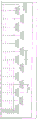
From fig. 13 and 14 it can be seen that: as mentioned before, it is possible to detect winding contact early, referred to as first event in fig. 13 and second event in fig. 14.
The verification is carried out here on the basis of the history and the associated tab 213, so that the analysis can be carried out again afterwards and retrospectively on the basis of the previously described functional sequence in fig. 10: what happens. A 2h time grid is employed and plotted, as also shown in fig. 10, wherein the device PHOT-0900 is displayed for the alarm situation of fig. 13 via the functionality selection field 237.
For the second event in FIG. 14, the device PHOT-1000 calls up in the functionality selection field 237 and uses a scale of 2h per scale grid in both diagrams.
The time range 300 is enlarged in fig. 13 with a partial enlargement to 300' in order to illustrate that the fault situation (occurrence of a 7% resistance change) starts at the time point 310. The break in resistance is shown after 5h at 320 as a true fault condition. However, the alarm generation when a real fault condition is observed (imminent) is earlier in time and has been classified by the system as a fault condition before the real fault has failed the thermal system (and the loaded lot is not available).
The time range 300 is enlarged in fig. 14 to 300 ″ with a similar partial enlargement in order to illustrate the beginning of the second event (fault situation 2) (here again a 7% resistance change occurs at time 310'). The break in resistance is shown as a second true failure condition after 3.5 hours at 320'. Alarm generation has occurred 3.5 hours ago.
Early identification of certificate … …
Two events (shown in fig. 13 and 14) that identify winding contact (first event and second event) early can be confirmed from the time the heater monitoring device was installed on applicants' internal equipment.
In both cases there was a resistance change of about 7% and a winding break (break of the heating coil in the thermal apparatus) occurred after about 3.5 hours or 5 hours.
The production team is saved by the alarm notification(s) to the device.
Claims (23)
1. A method for monitoring or supervising a thermal apparatus (100) for containing and annealing a wafer lot or wafer batch,
wherein the resistance value (R) to the resistor (1) in at least one heating zone (1 ') of the plurality of heating zones (1', 2 ', 3', 4 ', 5') of the thermal device (100)1) Making a continuous applied measurement;
the respective currently measured value (R) of the electrical resistance (1) in the associated heating zone (1') is measured1(i) With a previously measured value (R) of the same resistance (1)1(i-1)) to perform a comparison;
already at the two resistance values (R) from the same heating zone (1')/s1(i);R1(i-1)) detecting a deviation (310, Δ R) by comparison1) In the event of a failure of the entire heating zone (1') of the thermal device (100), a warning or alarm (90) is generated for the thermal device (100).
2. The method of claim 1, wherein the first and second light sources are selected from the group consisting of,
wherein the value (R) of the resistance (1) is determined from a plurality of measurements of the voltage (21) and the current (31) at the resistance (1)1) Resulting in a measure of the continued application of resistance.
3. The method of claim 2, wherein the first and second light sources are selected from the group consisting of,
wherein for the resistance value (R)1) The continuously applied measurement of (1) yields the value (R) of the resistance (1)1(i) In particular, a time profile for the ith sample value is derived.
4. The method according to at least claim 1,
wherein the generated warning or the generated alarm (90) for the thermal device causes a change of the electrical resistance (1) in the heating zone (1').
5. The method according to at least claim 1,
wherein for the resistance value (R)1) Or the continuously applied measurement of the electrical resistance (1) is also extended over a time range prior to the actual operation of the thermal device (100).
6. The method according to at least claim 1,
wherein electrical contacts (F) are electrically contacted at the parts (1.3, 1.4) of the heating coil as the resistor (1) which are arranged side by side1) The deviation (Delta R) of two resistance values separated in time and detected by comparison1) Before the break (320) of the interrupted current of the heating coil as a resistance (1).
7. The method according to at least claim 1,
wherein the deviation (Δ R) of two temporally spaced resistance values is detected by comparison1) Less than the resistance value (R) of a sound, undamaged heating coil (1)1) 10% of the total.
8. The method according to at least claim 7,
wherein the deviation of the two temporally spaced resistance values detected by the comparison is less than 7%, in particular less than 5%, of the value of a sound, undamaged heating coil (1).
9. The method of at least claim 1 or any one of claims 2 to 8,
wherein a break of the heating coil (1) is detected by detecting two temporally spaced and measured resistance values (R)1(i),R1(i-1)) deviation (Δ R) detected by comparison1) Then muchOver an hour.
10. The method of claim 1 or claim 9,
wherein the detected deviation (Δ R)1) Before the heating zone (1') with the associated heating resistor as a heating coil (1) fails.
11. The method according to any one of the preceding claims,
wherein the respective resistances are measured and compared continuously in a plurality of the hot zones or heating zones (1 ', 2 ', 3 ', 4 ', 5 ').
12. The method according to any one of the preceding claims,
wherein the respective resistances are measured and compared continuously in a plurality of thermal zones or heating zones (1 ', 2 ', 3 ', 4 ', 5 ') of a plurality of apparatuses (100).
13. The method according to any one of the preceding claims,
wherein the continuously applied measurement is also carried out if the thermal device (100) or its thermal zones (1 ', 2', … …) or one of its thermal zones is cooled or is in a cooling operation.
14. The method according to any one of the preceding claims,
there are several thresholds (122, 142, 151) that must be overcome during the measurement, and an alarm (90, 61, 161) is triggered by automatically deducing (151a) from the measurement.
15. The method of claim 14, wherein
(a) The minimum number of periods of the voltage feeding the respective resistor (1) must be switched on in sequence by the associated power control device (40), in particular a thyristor control device;
and/or
(b) Calculating and comparing the effective power from the calculated resistance (149) and from the measured voltage and from the measured current, respectively;
and/or
(c) The resistance difference (Delta R) calculated from the detected sum1) Experiences or experiences an inspection window and the resistance difference must leave the inspection window.
16. The method of claim 15, wherein the first and second light sources are selected from the group consisting of,
wherein at least four cycles are switched on, and/or the calculated effective powers should differ by less than 2% from each other, and/or the calculated resistance difference (Δ R) has to be detected1) At least 2.5%.
17. The method according to any one of the preceding claims,
in order to achieve a cleaner root mean square of the current and voltage at one or more of the resistors, the zero crossings are filtered out and only one half-wave, in particular the negative half-wave, is used for the evaluation.
18. A screen display for monitoring a plurality of thermal devices (100) or for performing the method according to any one of the preceding claims, the screen display having:
(i) a configuration window area (211) for displaying technical parameters of the thermal device (100), the configuration window area being in the form of: a first zone (321) with partitions (221a, 221b) for configuring the sampling rate and the number of sampled values, a second zone (222) for presetting the window size for the calculated resistance value, and a third zone (224, 224a) for activating or deactivating the hot zone (1 ', 2', … …) in the thermal device (100), and a fourth zone (223) for activating or deactivating the entire thermal device;
(ii) a measurement and detection window area (212) for displaying technical measurements of one of the thermal instruments (100), the measurement and detection window area being in the form of: at least three calculated resistance values for the actual or calculated measured values (23a), in particular for each hot zone of the thermal device (100)A further zone (230, 232, 91) for visual arrangement, a zone (91) for alarm notification (90), and a zone for displaying the calculated resistance value (R)1(i) ) of the time profile.
19. The screen display of claim 18,
wherein a plurality of measurement and detection window areas (212a, 212b) are provided and each measurement and detection window area is associated with a thermal apparatus (100).
20. Thermal device with a monitoring device for carrying out the method according to one of the preceding method claims for monitoring a thermally treated group of wafers or batch of wafers, in particular with a screen display according to claim 18 or 19.
21. The thermal device of claim 20,
wherein a computing device and a comparator (54) are provided, wherein
In the computing device (140), the currently measured values (R) of the electrical resistance (1) of the associated heating zones (1') can be respectively determined1(i) With a previously measured value (R) of the same resistance (1)1(i-1)) were compared.
22. The thermal device of claim 21,
wherein a deviation (310, Δ R) has been detected by comparison between two resistance values from the same heating zone (1')/in the heating zone1) Can cause or generate a warning or alarm (90) for the thermal device (100), which warning or alarm precedes in time the failure of one or the entire heating zone (1') in the thermal device (100).
23. The thermal device of claim 22,
wherein the comparator (144, 54) is a subtractor.
Applications Claiming Priority (5)
| Application Number | Priority Date | Filing Date | Title |
|---|---|---|---|
| DE102017122205 | 2017-09-25 | ||
| DE102017122205.7 | 2017-09-25 | ||
| DE102018101010.9A DE102018101010A1 (en) | 2017-09-25 | 2018-01-18 | Real-time monitoring of a multi-zone vertical furnace with early detection of a failure of a heating zone element |
| DE102018101010.9 | 2018-01-18 | ||
| PCT/IB2018/057414 WO2019058358A1 (en) | 2017-09-25 | 2018-09-25 | Real-time monitoring of a multi-zone vertical furnace with early detection of a failure of a heating zone element |
Publications (1)
| Publication Number | Publication Date |
|---|---|
| CN111433547A true CN111433547A (en) | 2020-07-17 |
Family
ID=65638366
Family Applications (1)
| Application Number | Title | Priority Date | Filing Date |
|---|---|---|---|
| CN201880062066.XA Pending CN111433547A (en) | 2017-09-25 | 2018-09-25 | Real-time monitoring and early identification of hot zone component failure for multi-zone vertical furnace |
Country Status (8)
| Country | Link |
|---|---|
| US (1) | US20200411343A1 (en) |
| EP (1) | EP3688394A1 (en) |
| JP (2) | JP7271520B2 (en) |
| KR (1) | KR102598971B1 (en) |
| CN (1) | CN111433547A (en) |
| DE (1) | DE102018101010A1 (en) |
| TW (1) | TWI808996B (en) |
| WO (1) | WO2019058358A1 (en) |
Families Citing this family (2)
| Publication number | Priority date | Publication date | Assignee | Title |
|---|---|---|---|---|
| CN113063999B (en) * | 2021-03-11 | 2023-08-18 | 北京北方华创微电子装备有限公司 | Method and system for diagnosing heater in semiconductor process equipment |
| CN116302773A (en) * | 2021-12-03 | 2023-06-23 | 株洲瑞德尔智能装备有限公司 | Fault monitoring method and device for sintering equipment |
Citations (6)
| Publication number | Priority date | Publication date | Assignee | Title |
|---|---|---|---|---|
| JP2002352938A (en) * | 2001-05-28 | 2002-12-06 | Tokyo Electron Ltd | Disconnection predicting method for heater element wire of heat treatment device, and the heat-treating device |
| JP2006085907A (en) * | 2004-09-14 | 2006-03-30 | Kokusai Electric Semiconductor Service Inc | Power supply device and semiconductor manufacturing apparatus |
| JP2006165200A (en) * | 2004-12-06 | 2006-06-22 | Kokusai Electric Semiconductor Service Inc | Resistance value detecting device of resistance heating heater in semiconductor manufacturing device and deterioration diagnosis device of resistance heating heater and network system in semiconductor manufacturing device |
| JP5098806B2 (en) * | 2008-05-21 | 2012-12-12 | 東京エレクトロン株式会社 | Electric power use disconnection prediction device and heat treatment device |
| US8791392B2 (en) * | 2010-10-22 | 2014-07-29 | Lam Research Corporation | Methods of fault detection for multiplexed heater array |
| JP5567318B2 (en) * | 2009-11-20 | 2014-08-06 | 株式会社国際電気セミコンダクターサービス | Power supply system, substrate processing apparatus, semiconductor manufacturing apparatus, and deterioration diagnosis method |
Family Cites Families (13)
| Publication number | Priority date | Publication date | Assignee | Title |
|---|---|---|---|---|
| DE3910676C2 (en) * | 1989-04-03 | 1999-03-04 | Pierburg Ag | Air mass flow measuring device |
| DE19643698C2 (en) * | 1996-05-11 | 2000-04-13 | Aeg Hausgeraete Gmbh | Device for shielding conductor tracks of a hob used for capacitive measurements |
| JP3988942B2 (en) * | 2003-03-31 | 2007-10-10 | 株式会社国際電気セミコンダクターサービス | Heater inspection apparatus and semiconductor manufacturing apparatus equipped with the same |
| JP4326570B2 (en) * | 2007-04-17 | 2009-09-09 | 東京エレクトロン株式会社 | Heater wire life prediction method, heat treatment apparatus, recording medium, heater wire life prediction processing system |
| US20090035463A1 (en) * | 2007-08-03 | 2009-02-05 | Tokyo Electron Limited | Thermal processing system and method for forming an oxide layer on substrates |
| TWI348726B (en) * | 2007-08-07 | 2011-09-11 | United Microelectronics Corp | Semiconductor equipment and breakdown precautionary system and method thereof |
| US7675307B2 (en) * | 2008-03-18 | 2010-03-09 | Star Technologies Inc. | Heating apparatus for semiconductor devices |
| FR2934083B1 (en) * | 2008-07-17 | 2010-09-10 | St Microelectronics Rousset | METHOD AND DEVICE FOR ADJUSTING THE DEPOSITION POSITION OF A SEMICONDUCTOR WAFER IN AN OVEN |
| WO2012165174A1 (en) | 2011-06-01 | 2012-12-06 | シャープ株式会社 | Device and method for detecting degradation of resistance heating heater |
| DE102011077970A1 (en) | 2011-06-22 | 2012-12-27 | Wacker Chemie Ag | Apparatus and process for the temperature treatment of corrosive gases |
| JP5876348B2 (en) | 2012-03-27 | 2016-03-02 | 東京エレクトロン株式会社 | Heater wire inspection method |
| JP2017073498A (en) * | 2015-10-08 | 2017-04-13 | 株式会社ニューフレアテクノロジー | Vapor phase epitaxial device and malfunction detection method |
| DE102016120569B4 (en) * | 2016-10-27 | 2018-07-19 | Hermann Betz | Electrically adjustable temperature sensor device of a heating system |
-
2018
- 2018-01-18 DE DE102018101010.9A patent/DE102018101010A1/en active Pending
- 2018-09-20 TW TW107133185A patent/TWI808996B/en active
- 2018-09-25 WO PCT/IB2018/057414 patent/WO2019058358A1/en unknown
- 2018-09-25 KR KR1020207010728A patent/KR102598971B1/en active IP Right Grant
- 2018-09-25 EP EP18799591.5A patent/EP3688394A1/en active Pending
- 2018-09-25 US US16/649,833 patent/US20200411343A1/en active Pending
- 2018-09-25 CN CN201880062066.XA patent/CN111433547A/en active Pending
- 2018-09-25 JP JP2020517118A patent/JP7271520B2/en active Active
-
2023
- 2023-04-26 JP JP2023071909A patent/JP2023109763A/en not_active Withdrawn
Patent Citations (6)
| Publication number | Priority date | Publication date | Assignee | Title |
|---|---|---|---|---|
| JP2002352938A (en) * | 2001-05-28 | 2002-12-06 | Tokyo Electron Ltd | Disconnection predicting method for heater element wire of heat treatment device, and the heat-treating device |
| JP2006085907A (en) * | 2004-09-14 | 2006-03-30 | Kokusai Electric Semiconductor Service Inc | Power supply device and semiconductor manufacturing apparatus |
| JP2006165200A (en) * | 2004-12-06 | 2006-06-22 | Kokusai Electric Semiconductor Service Inc | Resistance value detecting device of resistance heating heater in semiconductor manufacturing device and deterioration diagnosis device of resistance heating heater and network system in semiconductor manufacturing device |
| JP5098806B2 (en) * | 2008-05-21 | 2012-12-12 | 東京エレクトロン株式会社 | Electric power use disconnection prediction device and heat treatment device |
| JP5567318B2 (en) * | 2009-11-20 | 2014-08-06 | 株式会社国際電気セミコンダクターサービス | Power supply system, substrate processing apparatus, semiconductor manufacturing apparatus, and deterioration diagnosis method |
| US8791392B2 (en) * | 2010-10-22 | 2014-07-29 | Lam Research Corporation | Methods of fault detection for multiplexed heater array |
Also Published As
| Publication number | Publication date |
|---|---|
| WO2019058358A1 (en) | 2019-03-28 |
| EP3688394A1 (en) | 2020-08-05 |
| TWI808996B (en) | 2023-07-21 |
| JP7271520B2 (en) | 2023-05-11 |
| JP2020535646A (en) | 2020-12-03 |
| DE102018101010A1 (en) | 2019-03-28 |
| JP2023109763A (en) | 2023-08-08 |
| US20200411343A1 (en) | 2020-12-31 |
| TW201923368A (en) | 2019-06-16 |
| KR102598971B1 (en) | 2023-11-03 |
| KR20200100602A (en) | 2020-08-26 |
Similar Documents
| Publication | Publication Date | Title |
|---|---|---|
| US7489138B2 (en) | Differential arc fault detection | |
| JP2023109763A (en) | Real-time monitoring of multi-zone vertical furnace with early recognition of failure of heating element | |
| CN106483423B (en) | Fault searching method and device for breaker opening electric loop | |
| JP5888972B2 (en) | Solar power system | |
| US20200028349A1 (en) | System and method for detecting arc faults | |
| CN101071521B (en) | Method and device for monitoring detector line of fire detection system for faults | |
| KR101894474B1 (en) | Temperature Controller for Electric Mat Capable of Preventing Fire by Detecting Body Motion and Controlling Power Supply | |
| EP3396802A1 (en) | A method for identifying a fault event in an electric power distribution grid sector | |
| CN102054539A (en) | Detection method and device for nuclear power station temperature signal abrupt change | |
| CN109613426B (en) | Aging diagnosis method for plum blossom contact of high-voltage circuit breaker | |
| CN108474819A (en) | The method and apparatus of short circuit monitoring for threephase load | |
| CN110702246A (en) | Method and system for monitoring connection state of main loop of switch cabinet | |
| US6326598B1 (en) | Non-intrusive fault location system for an overheat detection system | |
| CN204373813U (en) | A kind of electric thermo-couple test furnace protective device | |
| KR101816896B1 (en) | Automatic Diagnosis System and Method for Electric Distribution Network | |
| US10910992B2 (en) | Method and device for detecting a stray electric arc in a photovoltaic installation | |
| Russell et al. | Preventing Certain Powerline Caused Wildfires by Early Detection and Repair of Failing Devices | |
| CN109856505B (en) | Immune time detection method for voltage sag | |
| CN113328524A (en) | Intelligent transformation of column switch based on FA | |
| JPH0387672A (en) | Diagnostic device for contact | |
| EP3317741B1 (en) | A safety circuit, a safety circuit operation method and an electrically operated motor comprising a safety circuit | |
| KR20210029057A (en) | Terminal block with CT / VT protection device for switch gear based on IoT technology | |
| JP2019178872A (en) | Fault locator | |
| CN109073688A (en) | Method for detecting the failure in the ammeter for including breaking units | |
| CN116027221A (en) | Method for identifying and locating periodic transient insulation faults of an ungrounded power system |
Legal Events
| Date | Code | Title | Description |
|---|---|---|---|
| PB01 | Publication | ||
| PB01 | Publication | ||
| SE01 | Entry into force of request for substantive examination | ||
| SE01 | Entry into force of request for substantive examination |