CN111190854A - Communication data processing method, device, equipment, system and storage medium - Google Patents
Communication data processing method, device, equipment, system and storage medium Download PDFInfo
- Publication number
- CN111190854A CN111190854A CN201911420234.0A CN201911420234A CN111190854A CN 111190854 A CN111190854 A CN 111190854A CN 201911420234 A CN201911420234 A CN 201911420234A CN 111190854 A CN111190854 A CN 111190854A
- Authority
- CN
- China
- Prior art keywords
- kernel
- data
- memory
- target
- address
- Prior art date
- Legal status (The legal status is an assumption and is not a legal conclusion. Google has not performed a legal analysis and makes no representation as to the accuracy of the status listed.)
- Granted
Links
- 230000006854 communication Effects 0.000 title claims abstract description 342
- 238000004891 communication Methods 0.000 title claims abstract description 340
- 238000003672 processing method Methods 0.000 title claims abstract description 21
- 238000012545 processing Methods 0.000 claims abstract description 246
- 238000000034 method Methods 0.000 claims abstract description 99
- 230000008569 process Effects 0.000 claims description 64
- 238000004590 computer program Methods 0.000 claims description 27
- 230000005540 biological transmission Effects 0.000 claims description 20
- 230000007246 mechanism Effects 0.000 claims description 17
- 238000012546 transfer Methods 0.000 description 12
- 238000010586 diagram Methods 0.000 description 10
- 230000001960 triggered effect Effects 0.000 description 8
- 238000011144 upstream manufacturing Methods 0.000 description 3
- 239000002699 waste material Substances 0.000 description 3
- 230000002457 bidirectional effect Effects 0.000 description 2
- 230000001360 synchronised effect Effects 0.000 description 2
- 230000002411 adverse Effects 0.000 description 1
- 230000001174 ascending effect Effects 0.000 description 1
- 230000006399 behavior Effects 0.000 description 1
- 230000000694 effects Effects 0.000 description 1
- 238000005516 engineering process Methods 0.000 description 1
- 230000008676 import Effects 0.000 description 1
- 230000003993 interaction Effects 0.000 description 1
- 239000004973 liquid crystal related substance Substances 0.000 description 1
- 235000013372 meat Nutrition 0.000 description 1
- 238000012986 modification Methods 0.000 description 1
- 230000004048 modification Effects 0.000 description 1
- 230000004044 response Effects 0.000 description 1
- 230000011664 signaling Effects 0.000 description 1
- 230000003068 static effect Effects 0.000 description 1
- XLYOFNOQVPJJNP-UHFFFAOYSA-N water Substances O XLYOFNOQVPJJNP-UHFFFAOYSA-N 0.000 description 1
Images


Classifications
-
- G—PHYSICS
- G06—COMPUTING; CALCULATING OR COUNTING
- G06F—ELECTRIC DIGITAL DATA PROCESSING
- G06F15/00—Digital computers in general; Data processing equipment in general
- G06F15/16—Combinations of two or more digital computers each having at least an arithmetic unit, a program unit and a register, e.g. for a simultaneous processing of several programs
- G06F15/163—Interprocessor communication
- G06F15/173—Interprocessor communication using an interconnection network, e.g. matrix, shuffle, pyramid, star, snowflake
- G06F15/17306—Intercommunication techniques
- G06F15/17331—Distributed shared memory [DSM], e.g. remote direct memory access [RDMA]
Abstract
The application relates to a communication data processing method, a communication data processing device, a communication data processing equipment, a communication data processing system and a storage medium. The method is applied to a communication data processing system, the communication data processing system comprises a first kernel, a second kernel, a shared memory and an FPGA, and the method comprises the following steps: controlling the first kernel to receive a first trigger instruction sent by the FPGA, and sending at least one group of communication data to a shared memory for storage according to the first trigger instruction; and controlling the second kernel to receive a second trigger instruction sent by the FPGA, and processing the communication data on the shared memory according to the second trigger instruction. The method can improve the communication real-time performance of the communication data processing system.
Description
Technical Field
The present application relates to the field of communication data processing technologies, and in particular, to a communication data processing method, apparatus, device, system, and storage medium.
Background
In the SOC + LINUX device, a high-speed internal bus is provided inside a low-cost SOC (system on chip), and communication among a plurality of cores inside the SOC can be realized through the bus, and a general SOC may include a plurality of cores, such as a CPU, a DSP, an ARM, and the like. Generally, when communication is needed among a plurality of cores, triggering of inter-core communication may generally adopt an interrupt mode, that is, an interrupt mode may be sent among the cores, and bidirectional transmission of data may be performed in the interrupt time period.
At present, in the process of inter-core communication between a CPU core and a DSP core, according to the above behavior example, the DSP needs to copy data from a bus for processing, and transmit the data to the bus after the processing is completed, the CPU copies data sent from the DSP from the bus for processing within an interrupt time, and sends the data to a server and the like after the processing.
However, in the above-described technique, when performing inter-core communication, the CPU processing speed is low and the DSP processing speed is high, which causes a problem of low real-time communication performance.
Disclosure of Invention
In view of the above, it is necessary to provide a communication data processing method, apparatus, device, system, and storage medium capable of real-time communication.
A communication data processing method is applied to a communication data processing system, the communication data processing system comprises a first kernel, a second kernel, a shared memory and an FPGA, and the method comprises the following steps:
controlling the first kernel to receive a first trigger instruction sent by the FPGA, and sending at least one group of communication data to a shared memory for storage according to the first trigger instruction;
and controlling the second kernel to receive a second trigger instruction sent by the FPGA, and processing the communication data on the shared memory according to the second trigger instruction.
In one embodiment, the processing the communication data on the shared memory includes:
performing processing operations, the processing operations comprising: controlling the second kernel to acquire a data processing completion identifier on the shared memory, and determining a corresponding target address according to the data processing completion identifier; and controlling the second kernel to process the target communication data on the target address on the shared memory, and clearing the target address after the processing is finished.
In one embodiment, the method further comprises:
and controlling the second kernel to judge whether the shared memory has a data processing completion identifier, and if so, returning to execute the processing operation until the data processing completion identifier does not exist in the shared memory.
In one embodiment, the target communication data includes target communication short data and target communication long data, and the shared memory includes an inter-core memory and an external memory; the controlling the second kernel to obtain a data processing completion identifier on the shared memory, and determining a corresponding target address according to the data processing completion identifier includes:
controlling the second kernel to acquire the data processing completion identifier on the inter-kernel memory, and determining the target address according to the data processing completion identifier; the target address is used for storing target communication short data, a transmission identifier and an address of target communication long data, and the transmission identifier is used for representing whether the target communication data are stored in an inter-core memory and an external memory in a distributed mode;
controlling the second kernel to determine whether the target communication data is stored in the inter-kernel memory and the external memory in a distributed manner according to the transmission identifier on the target address in the inter-kernel memory;
and if so, controlling the second kernel to acquire target communication long data on the external memory.
In one embodiment, the controlling the second kernel to obtain the target communication long data on the external memory includes:
controlling the second kernel to acquire the address of the target communication long data on the target address on the inter-kernel memory;
and controlling the second kernel to acquire the corresponding target communication long data on the external memory according to the address of the target communication long data.
In one embodiment, the controlling the second core to process the target communication data at the target address on the shared memory, and to clear the target address after the processing is completed includes:
controlling the second kernel to process the target communication short data, and clearing the address of the target communication short data in the inter-kernel memory after the processing is finished;
and if the target communication data is stored in the inter-core memory and the external memory in a distributed manner, controlling the second core to process the target communication long data, and clearing the address of the target communication long data in the external memory after the processing is finished.
In one embodiment, the controlling the second core to process the target communication data at the target address on the shared memory, and to clear the target address after the processing is completed includes:
and if the target communication data is stored in the inter-core memory, controlling the second core to process the target communication short data, and clearing the address of the target communication short data in the inter-core memory after the processing is finished.
In one embodiment, the trigger mechanism of the first trigger instruction and the trigger mechanism of the second trigger instruction are different, and the trigger mechanism is used for characterizing the interrupt frequency of the kernel.
In one embodiment, the method further comprises:
and setting a plurality of pipeline state machines which are respectively used for recording the processing states of the services of the first kernel and the second kernel.
A communication data processing device is applied to a communication data processing system, the communication data processing system comprises a first kernel, a second kernel, a shared memory and an FPGA, and the device comprises:
the first control module is used for controlling the first kernel to receive a first trigger instruction sent by the FPGA and sending at least one group of communication data to the shared memory for storage according to the first trigger instruction;
and the second control module is used for controlling the second kernel to receive a second trigger instruction sent by the FPGA and processing the communication data on the shared memory according to the second trigger instruction.
A computer device comprising a memory and a processor, the memory storing a computer program, the processor implementing the following steps when executing the computer program:
controlling the first kernel to receive a first trigger instruction sent by the FPGA, and sending at least one group of communication data to a shared memory for storage according to the first trigger instruction;
and controlling the second kernel to receive a second trigger instruction sent by the FPGA, and processing the communication data on the shared memory according to the second trigger instruction.
A communication data processing system comprises a shared memory, an FPGA, a first kernel and a second kernel, wherein:
the first kernel is used for receiving a first trigger instruction sent by the FPGA and sending at least one group of communication data to the shared memory for storage;
the second kernel is used for receiving a second trigger instruction sent by the FPGA and processing the communication data on the shared memory;
and the FPGA is used for sending a first trigger instruction to the first kernel and sending a second trigger instruction to the second kernel.
A readable storage medium having stored thereon a computer program which, when executed by a processor, performs the steps of:
controlling the first kernel to receive a first trigger instruction sent by the FPGA, and sending at least one group of communication data to a shared memory for storage according to the first trigger instruction;
and controlling the second kernel to receive a second trigger instruction sent by the FPGA, and processing the communication data on the shared memory according to the second trigger instruction.
The communication data processing method, the device, the equipment, the system and the storage medium are applied to a communication data processing system, the communication data processing system comprises a first kernel, a second kernel, a shared memory and an FPGA, in the method, the system can control the first kernel to receive a first trigger instruction sent by the FPGA, send at least one group of communication data to the shared memory for storage according to the first trigger instruction, control the second kernel to receive a second trigger instruction sent by the FPGA, and process the communication data on the shared memory according to the second trigger instruction. In the method, when the first kernel and the second kernel receive and transmit communication data, macro scheduling can be performed through FPGA external interruption without extra consumption of resources of the first kernel and the second kernel to trigger, so that resource waste and waiting time of the first kernel and the second kernel can be reduced, repeated invalid interruption is reduced, and the processing efficiency of the system is improved; in addition, when the first kernel and the second kernel receive and transmit data, the data can be processed on the shared memory directly without copying from the bus, so that the time consumption of the first kernel and the second kernel for processing the data can be reduced, the extra useless expenditure of the first kernel and the second kernel can be saved, the real-time processing capability of the system can be improved, namely the real-time performance is improved, and the purpose of changing the time by the space is achieved.
Drawings
FIG. 1 is a schematic diagram of a communications data processing system in one embodiment;
FIG. 2a is a schematic flow chart diagram illustrating a method for a communication data processing system in one embodiment;
FIG. 2b is a block diagram of a pipeline state machine in one embodiment;
FIG. 2c is a flow diagram illustrating an example of an up-down communication process;
FIG. 3 is a schematic flow chart diagram of a method of a communication data processing system in another embodiment;
FIG. 4 is a schematic flow chart diagram of a method for a communication data processing system in accordance with another embodiment;
FIG. 5 is a schematic flow chart diagram of a method for a communication data processing system in accordance with another embodiment;
FIG. 6 is a block diagram of an apparatus in a communication data processing system in one embodiment;
FIG. 7 is a diagram illustrating an internal structure of a computer device according to an embodiment.
Detailed Description
In order to make the objects, technical solutions and advantages of the present application more apparent, the present application is described in further detail below with reference to the accompanying drawings and embodiments. It should be understood that the specific embodiments described herein are merely illustrative of the present application and are not intended to limit the present application.
At present, in SOC + LINUX devices, a high-speed internal bus is provided inside a low-cost SOC to implement inter-core communication, and an interrupt mode is adopted for triggering inter-core communication. Multiple pairs of interrupts of different business entities exist among cores, and in each message processing flow, data is processed by the following processing links: descending: 1. the CPU obtains the network message through kernel interruption, the priority is high, and burst cannot be avoided; 2. the service entity processes data, distributes the data to a DSP or an inner core entity and triggers interruption; 3. the DSP core interrupts the response, receives and processes the data; 4. and the DSP core processes the data and forwards the data to the terminal. Ascending: 1. the DSP receives terminal data and processes the data; 2. triggering interruption by the DSP core, and distributing data to the CPU entity; 3. the CPU service entity responds to the interrupt, receives and processes the data; 4. the CPU forwards the network data through a kernel interrupt. The CPU runs a LINUX multitask preemptive system, and there are various kernel interrupt processes, such as: the access of external devices such as a serial port, an I2C and a network port is generally higher in priority than external interruption, the real-time performance of the LINUX system with a real-time patch is still a short board, particularly the real-time performance is not good under the conditions of low time delay, high bandwidth, high throughput and the like of a low-cost SOC, and the real-time performance is high because a DSP core processes data through circulating water in a priority + interruption mode after BOOT initializes hardware. From the above processing flows, it can be found that, when processing one packet, the CPU core where the LINUX is inevitably slower than the DSP core, and therefore, the communication real-time performance of the entire communication system is affected, and many adverse effects are brought. Embodiments of the present application provide a communication data processing method, apparatus, device, system, and storage medium, which are used to solve the above problems.
The communication data processing method provided by the embodiment of the application can be applied to a communication data processing system, as shown in fig. 1, the communication data processing system includes a first kernel 101, a second kernel 102, a shared memory 103, and an FPGA104, where the first kernel 101 is configured to receive a first trigger instruction sent by the FPGA104, and send at least one group of communication data to the shared memory 103 for storage; the second core 102 is configured to receive a second trigger instruction sent by the FPGA104, and process communication data on the shared memory 103; the FPGA104 is configured to send a first trigger instruction to the first core 101 and send a second trigger instruction to the second core 102. The first core 101 and the second core 102 may be a DSP, a CPU, an ARM, etc., but the first core 101 and the second core 102 are different, for example, the first core 101 is a DSP, the second core 102 may be a CPU, an ARM, etc., and may not be a DSP, in addition, the first core 101 and the second core 102 may be chips inside an SOC, that is, cores both belonging to the SOC, the shared memory 103 may be a memory inside the SOC, or a memory formed by a memory inside the SOC and an external memory, the FPGA104 may be a chip outside the SOC, and may perform data communication with the first core 101 and the second core 102. In addition, the CPU in the embodiment of the present application refers to a Central Processing Unit, the DSP refers to Digital signal Processing, and the FPGA refers to a Field Programmable Gate Array.
It should be noted that the execution subject of the embodiment of the present application may be a communication data processing apparatus, a communication data processing system, or a computer device in a communication data processing system, and the following description takes a communication data processing system as an execution subject.
In an embodiment, the embodiment relates to a specific process of how to trigger a first kernel and a second kernel through an FPGA to enable the first kernel and the second kernel to complete data transceiving on a shared memory. The method may be applied to a communication data processing system, where the communication data processing system includes a first core, a second core, a shared memory, and an FPGA, and as shown in fig. 2a, the method may include the following steps:
s202, controlling the first kernel to receive a first trigger instruction sent by the FPGA, and sending at least one group of communication data to the shared memory for storage according to the first trigger instruction.
And S204, controlling the second kernel to receive a second trigger instruction sent by the FPGA, and processing the communication data on the shared memory according to the second trigger instruction.
In this embodiment, taking a communication uplink process as an example, the first core may be a DSP, the second core may be a CPU, and as an example, the first core may be a CPU, the second core may be a DSP, a general operating system LINUX may run on the CPU, and an operating system may not run on the DSP, so that a speed of processing data by the CPU may be relatively slow compared to that by the DSP, the CPU may be generally referred to as a slow core, and the DSP may be referred to as a fast core. In this embodiment, the FPGA mainly sends a trigger instruction to the first core and the second core, so that the first core and the second core operate, when the FPGA sends the trigger instruction, the trigger instruction may be triggered at regular time, where the trigger instruction may be an interrupt trigger instruction, if the FPGA sends the trigger instruction to the DSP, the sent trigger instruction may include two parts of content, where the first part is used to instruct the DSP to start to operate, and the second part is used to instruct the DSP to operate the content or the flow that needs to operate, such as to receive and transmit data; if the FPGA sends the trigger instruction to the CPU, the trigger instruction sent may only include content for indicating that the CPU needs to work, such as sending and receiving data. Secondly, optionally, in this embodiment, the trigger mechanisms of the first trigger instruction and the second trigger instruction are different, and the trigger mechanisms are used to characterize the interrupt frequency of the cores, that is, in the communication process, the time intervals for sending the first trigger instruction and the second trigger instruction are also different, that is, the interrupt frequency sent to the first core and the second core is different. For example, assuming that the first core is a DSP and the second core is a CPU, or the first core is a CPU and the second core is a DSP, the interrupt frequency sent by the FPGA to the DSP and the CPU is different, for example, a trigger instruction may be sent to the CPU every 5 minutes and a trigger instruction may be sent to the DSP every 1 minute. In addition, when the trigger instruction sent by the FPGA to the first core and the meat core causes the first core or the second core to process data, the time needs to be controlled within the effective time of the communication data, that is, between the interrupts sent by the FPGA to the first core or the second core.
In addition, the shared memory may be an internal memory inside the SOC, or an internal memory inside the SOC and an external memory, and this embodiment mainly adopts the shared memory as an internal memory inside the SOC and an external memory, where the external memory may be a DDR (Double Data Rate) external to the SOC, and the like, and secondly, the shared memory may include a two-level ring memory and an information management area, where the information management area may store use information of an address space in the shared memory and provide for both a first core and a second core to obtain an address and a release address, the two-level ring memory may be used for fast reading and writing by the first core and the second core, the two-level ring memory is an internal memory inside the SOC, i.e., an inter-core memory, and is marked as a first cache, and the external DDR of the SOC is marked as a second cache, the first cache has a fast access speed but a small space, and is generally used for storing some non-communication identification, address, signaling, heartbeat, notification type information and the like, and the second cache has a large space but a slow access speed, and is generally used for method interaction communication data. Further, according to the communication processing capacity of the CPU and the DSP, the first cache is distributed into 1024 × 2 circular queues for each group of communication entities in a bidirectional mode, and each address space is 10 bytes; the second cache is divided into 1024 × 2 circular queues for each group of communication entities, and each address space is 1 kbyte; each group of communication entities here refers to different groups of communication data that are mutually transmitted by two communication parties, for example, the CPU sends a1 to the DSP, the DSP sends a2 to the CPU, and a1 and a2 can be regarded as a group of communication entities.
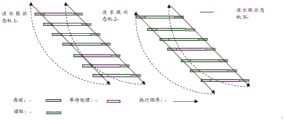
On the other hand, in this embodiment, optionally, the system may further preset a plurality of pipeline state machines, which are respectively used for recording the processing states of the services of the first core and the second core. Referring to fig. 2b, each pipeline state machine correspondingly processes a group of communication entities, and stores data, waits for processing, reads, and the like according to the execution sequence, taking the DSP and the CPU as an example, the state of each pipeline state machine may include a processing state of the DSP and the CPU, for example, the processing state of each pipeline state machine on the DSP may include: the FPGA triggers DSP to work, processes air interface messages, releases addresses, acquires available addresses, stores data and the like, and the processing state of each group of pipeline state machines on the CPU can comprise: the FPGA regularly triggers the CPU to receive, acquire an available address, prefetch a short message, process message data, release an address and the like. In the uplink and the downlink, the FPGA can rotate to trigger the kernel, so that the kernel executes a plurality of processing states of the plurality of pipeline state machines.
Specifically, when the first core and the second core communicate with each other, and when the first core and the second core communicate with each other, for example, the first core is a CPU, the second core is a DSP, and after the CPU is triggered by the FPGA at regular time (certainly, the CPU can be scheduled by LINUX at downlink, and the FPGA is not required to be triggered, both can be), the CPU can search for an available address space on the shared memory, and send at least one set of processed communication data to the available address space for storage after the CPU is found, and in the shared memory, generally one set of communication data can be stored in one address space of the downlink queue correspondingly, by which each set of communication data sent by the CPU can be stored in different address spaces of the shared memory, after the CPU finishes storing, the CPU can return to its own program for execution without waiting for the DSP to fetch data for return, and after the DSP is triggered by the FPGA at regular time, the DSP can directly read the address where the communication data are stored on the shared memory, and the read address is directly imported into a DSP program, the DSP program directly runs on the shared memory, the data on the address space corresponding to the address is directly processed, the data on the address space does not need to be copied into the DSP program for processing, the processing result can be obtained after the DSP processing, the generally obtained processing result can be transmitted to a terminal through the FPGA and a high-speed bus, and the processing result can not be transmitted when the downloading is not needed.
In addition, when in upstream communication, taking the first kernel as the DSP and the second kernel as the CPU as an example, after the DSP is triggered by the FPGA at regular time, the DSP may also search an available address space of the upstream queue on the shared memory, and send at least one set of processed communication data to the available address space for storage after the DSP is found, where a set of communication data is also stored in the address space of an upstream queue correspondingly, by which each set of communication data sent by the DSP may be stored in different address spaces of the shared memory, after the DSP finishes storing, the DSP may return its current program to execute without waiting for the CPU to fetch data to return, and after the CPU is triggered by the FPGA at regular time, the CPU may directly read the address stored with the communication data from the shared memory and directly import the read address into the CPU program, the CPU program directly runs on the shared memory, the data in the address space corresponding to the address is directly processed, the data in the address space is not required to be copied to a CPU program for processing, a processing result can be obtained after the CPU processes the data, and then information such as the processing result and the like can be transmitted to a server and the like through a bus.
The communication data processing method is applied to a communication data processing system, the communication data processing system comprises a first kernel, a second kernel, a shared memory and an FPGA, and the system can control the first kernel to receive a first trigger instruction sent by the FPGA, send at least one group of communication data to the shared memory for storage according to the first trigger instruction, control the second kernel to receive a second trigger instruction sent by the FPGA, and process the communication data on the shared memory according to the second trigger instruction. In the method, when the first kernel and the second kernel receive and transmit communication data, macro scheduling can be performed through FPGA external interruption without extra consumption of resources of the first kernel and the second kernel to trigger, so that resource waste and waiting time of the first kernel and the second kernel can be reduced, repeated invalid interruption is reduced, and the processing efficiency of the system is improved; in addition, when the first kernel and the second kernel receive and transmit data, the data can be processed on the shared memory directly without copying from the bus, so that the time consumption of the first kernel and the second kernel for processing the data can be reduced, the extra useless expenditure of the first kernel and the second kernel can be saved, the real-time processing capability of the system can be improved, namely the real-time performance is improved, and the purpose of changing the time by the space is achieved.
In another embodiment, another communication data processing method is provided, and this embodiment relates to a specific process of how the second kernel processes communication data on the shared memory, and clears the address after processing. On the basis of the above embodiment, the method may include the following step a:
step A, executing processing operation, wherein the processing operation comprises the following steps: controlling a second kernel to acquire a data processing completion identifier on the shared memory, and determining a corresponding target address according to the data processing completion identifier; and controlling the second kernel to process the target communication data on the target address on the shared memory, and clearing the target address after the processing is finished.
Here, the data processing completion flag may be a number, a letter, a symbol, or the like. In addition, the data processing completion flag may be only one cache one, or may be both the cache one and the cache two, which is not specifically limited in this embodiment.
Specifically, after the first core sends the processed communication data to the shared memory for storage, the first core may add a data processing completion identifier to each set of stored outgoing data, where the data processing completion identifier may be added to an address space for storing data, then the second core may search for whether there is a data processing completion identifier on the shared memory after being triggered at a fixed time, if there is a data processing completion identifier, sequentially read addresses corresponding to the data processing completion identifiers according to a certain sequence (for example, a sequence from the front to the back), where the addresses corresponding to the data processing completion identifiers may be marked as target addresses, and after the second core obtains the target addresses, the second core may obtain the communication data in the address space corresponding to the target addresses, and marked as target communication data, and then may process the target communication data, after the processing is completed, the address space corresponding to the target address may be emptied for the next storage use. It should be noted that, if multiple sets of target communication data are found, the second core may process the sets of target communication data according to a certain order (for example, an order from front to back) during processing, and each time a set of communication data is processed, the address space of the target address corresponding to the currently processed communication data may be emptied.
After the address space of the target address is cleared, optionally, the system may further control the second kernel to determine whether the shared memory has the data processing completion identifier, and if so, return to execute the processing operation until the shared memory does not have the data processing completion identifier. That is to say, after the second kernel clears the address space of the target address, because the first kernel continuously stores the processed data in the shared memory, after the second kernel completes the processing of the communication data corresponding to the currently found data processing completion identifier, the second kernel may further continue to determine whether the data processing completion identifier exists currently, and if the data processing completion identifier exists, the second kernel may return to execute step a above until the processing completion identifier does not exist in the shared memory, that is, the processed communication data stored in the first kernel does not exist.
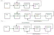
Referring to fig. 2c, in the uplink communication, on the DSP side, the FPGA triggers the DSP at regular time, and the DSP acquires an empty address (i.e., an empty address that can be stored) in the shared memory and stores data; and on the CPU side, the FPGA regularly triggers the CPU, the CPU fetches a message address from the shared memory (namely, acquires a target address with a data processing completion identifier), processes two-stage messages at the message address (namely, processes data on an address space of the target address, and the two stages refer to processing data on a first cache and a second cache), clears the address (namely, clears the target address with the data processing completion identifier on the first cache and the second cache), judges whether an unread message exists or not (namely, judges whether the data processing completion identifier exists in the shared memory or not), returns to execute the fetching of the message address if the unread message exists, and returns to regularly trigger the CPU if the data processing completion identifier does not exist. During downlink communication, the CPU can be managed and scheduled by LINUX, or triggered by FPGA to acquire an empty address and store data; and on the DSP side, the FPGA regularly triggers the DSP, the DSP fetches a message address from the shared memory (namely, obtains a target address with a data processing completion identifier), processes two-stage messages at the message address (namely, processes data on an address space of the target address, and the two stages refer to processing data on a first cache and a second cache), clears the address (namely, clears the target address with the data processing completion identifier on the first cache and the second cache), judges whether an unread message exists or not (namely, judges whether the data processing completion identifier exists in the shared memory or not), and if so, returns to execute the fetching of the message address, and if not, returns to regularly trigger the DSP.
In the communication data processing method provided in this embodiment, the system may control the second kernel to obtain the data processing completion identifier on the shared memory, determine the corresponding target address according to the data processing completion identifier, control the second kernel to process the target communication data on the target address on the shared memory, and clear the target address after the processing is completed. In this embodiment, the second kernel may find the target address where the data is stored according to the data processing completion identifier, so that blind search and time waste may be avoided.
In another embodiment, another communication data processing method is provided, where the embodiment relates to how the second core obtains target communication data on the inter-core memory and the external memory according to the data processing completion identifier if the target communication data includes target communication short data and target communication long data and the shared memory includes the inter-core memory and the external memory. On the basis of the foregoing embodiment, as shown in fig. 3, the controlling the second kernel to obtain the data processing completion identifier on the shared memory in step a, and determining the corresponding target address according to the data processing completion identifier may include the following steps:
s302, controlling a second kernel to acquire a data processing completion identifier on the inter-core memory, and determining a target address according to the data processing completion identifier; the target address is used for storing target communication short data, a transfer identifier and an address of the target communication long data, and the transfer identifier is used for representing whether the target communication data are stored on the inter-core memory and the external memory in a distributed mode.
S304, controlling the second kernel to determine whether the target communication data is stored in the inter-kernel memory and the external memory in a distributed manner according to the transmission identifier on the target address in the inter-kernel memory.
In this embodiment, the inter-core memory may be the first cache in S202 to S204, and the external memory may be the second cache in S202 to S204. The distributed storage means that target communication short data in the target communication data is stored on the inter-core memory, the target communication long data is stored on the external memory, and the non-distributed storage means that the target communication data is only stored on the inter-core memory. In addition, the data format stored in each address space in the inter-core memory is target communication short data bit + transfer identification bit + address bit of target communication long data, for example, the target communication data includes a + b, where a is the target communication short data, b is the target communication long data, and the format stored in one address space in the inter-core memory may be represented as a + transfer identification + b; the transfer identifier may be a letter, a number, a pattern, etc., and it may be known whether the target communication data is distributedly stored in the inter-core memory and the external memory according to the transfer identifier, for example, the transfer identifier is a number 0 or 1, if 1, the target communication data may be considered to be distributedly stored in the inter-core memory and the external memory, at this time, the address bit of the target communication long data may store the corresponding storage address of the target communication long data in the external memory, if 0, the target communication data may be considered to be only stored in the inter-core memory, and the external memory does not have the corresponding target communication data, at this time, the address bit of the target communication long data may be empty.
And S306, if yes, controlling the second kernel to acquire the target communication long data from the external memory.
In this embodiment, after determining that the target communication data is distributively stored in the inter-core memory and the external memory according to the transfer identifier, optionally, the method steps shown in fig. 4 may be adopted to obtain the target communication long data from the external memory, and as shown in fig. 4, S306 may include the following steps S402-S404:
s402, controlling the second kernel to obtain the address of the target communication long data on the target address on the inter-core memory.
And S404, controlling the second kernel to acquire the corresponding target communication long data from the external memory according to the address of the target communication long data.
Specifically, after the second core finds the data processing completion identifier on the shared memory, for any found data processing completion identifier, the corresponding target address may be obtained according to the data processing completion identifier, where the target address may be an address on the inter-core memory, and the corresponding address space may be found according to the target address, and on the address space, the target communication short data is found, and it is determined whether the external memory has the target communication long data corresponding to the same group of communication entities through the transfer identifier on the address space, and if the external memory exists, the address of the target communication long data may be obtained on the address bit behind the transfer identifier, and the corresponding target communication long data is found on the external memory through the address of the target communication long data.
In the communication data processing method provided in this embodiment, if the target communication data includes the target communication short data and the target communication long data, and the shared memory includes the inter-core memory and the external memory, the second core may obtain the target communication short data in the inter-core memory according to the data processing completion identifier, and obtain the target communication long data corresponding to the external memory when the target communication data is stored in a distributed manner according to the transfer identifier in the inter-core memory. In this embodiment, whether the long data of the target communication exists after the external memory can be judged according to the transfer identifier on the inter-core memory, and the method using the identifier is simple, so that whether the long data of the target communication exists on the external memory can be known simply and quickly by the method, and when the long data of the target communication exists on the external memory, the long data of the target communication can be processed quickly, so that a part of time can be saved, and the overall real-time performance of the system can be improved.
In another embodiment, another communication data processing method is provided, and this embodiment relates to a specific process that data can be further processed after target communication short data and/or target communication long data are obtained. On the basis of the above embodiment, in the processing, the data processing may be performed by using the method steps shown in fig. 5, and as shown in fig. 5, the processing steps may include the following steps:
and S502, controlling the second kernel to process the target communication short data, and clearing the address of the target communication short data in the inter-kernel memory after the processing is finished.
And S504, if the target communication data are stored in the inter-core memory and the external memory in a distributed manner, controlling the second core to process the target communication long data, and clearing the address of the target communication long data in the external memory after the processing is finished.
In this embodiment, if the target communication data is stored in the inter-core memory and the external memory in a distributed manner, the second core may first perform fast processing on the target communication short data in the inter-core memory, and map the target communication long data to the external memory according to the address of the target communication long data, find the target communication long data, and process the target communication long data, where data copying is not required, so that the processing speed of the second core may be increased, the real-time performance may be improved, and after the processing is completed, the address spaces of the group of target communication data in the inter-core memory and the external memory may be emptied for subsequent use.
In addition, optionally, if the target communication data is stored in the inter-core memory, the second core is controlled to process the target communication short data, and after the processing is completed, the address of the target communication short data in the inter-core memory is cleared. That is, if the target communication data is not distributedly stored in the inter-core memory and the external memory, and is mainly stored only in the inter-core memory, the second core may directly and quickly process the target communication data in the inter-core memory, and after the processing is completed, the address space of the target address of the target communication data in the inter-core memory is emptied, so as to facilitate subsequent use.
In the communication data processing method provided in this embodiment, if the target communication data is stored in the inter-core memory and the external memory at the same time, the data in the inter-core memory and the external memory may be processed in the inter-core memory and the external memory, and after the processing is completed, the address spaces corresponding to the inter-core memory and the external memory may be cleared, and if the target communication data is stored only in the inter-core memory, the address spaces corresponding to the inter-core memory may be cleared after the target communication data is processed in the inter-core memory. In this embodiment, since the address space corresponding to the processed data can be emptied, the address space can be conveniently reused subsequently, and the storage capacity of the shared memory is indirectly increased.
It should be understood that although the various steps in the flow charts of fig. 2a, 3-5 are shown in order as indicated by the arrows, the steps are not necessarily performed in order as indicated by the arrows. The steps are not performed in the exact order shown and described, and may be performed in other orders, unless explicitly stated otherwise. Moreover, at least some of the steps in fig. 2a, 3-5 may include multiple sub-steps or multiple stages that are not necessarily performed at the same time, but may be performed at different times, and the order of performance of the sub-steps or stages is not necessarily sequential, but may be performed in turn or alternating with other steps or at least some of the sub-steps or stages of other steps.
In one embodiment, a communication data processing system is provided, the system comprising a shared memory, an FPGA, a first core, and a second core, wherein:
the first kernel is used for receiving a first trigger instruction sent by the FPGA and sending at least one group of communication data to the shared memory for storage;
the second kernel is used for receiving a second trigger instruction sent by the FPGA and processing the communication data on the shared memory;
and the FPGA is used for sending a first trigger instruction to the first kernel and sending a second trigger instruction to the second kernel.
Optionally, the trigger mechanisms of the first trigger instruction and the second trigger instruction are different, and the trigger mechanisms are used for characterizing interrupt frequency of the kernel.
Optionally, the system may be configured with a plurality of pipeline state machines, which are respectively used to record the processing states of the services of the first core and the second core.
In another embodiment, the second core is further configured to perform processing operations, where the processing operations include: acquiring a data processing completion identifier on the shared memory, and determining a corresponding target address according to the data processing completion identifier; and controlling the second kernel to process the target communication data on the target address on the shared memory, and clearing the target address after the processing is finished.
Optionally, the second kernel is further configured to determine whether a data processing completion identifier exists on the shared memory, and if the data processing completion identifier exists on the shared memory, return to execute the processing operation until the data processing completion identifier does not exist on the shared memory.
In another embodiment, the target communication data includes target communication short data and target communication long data, and the shared memory includes an inter-core memory and an external memory; the second kernel is further configured to obtain the data processing completion identifier on the inter-kernel memory, and determine the target address according to the data processing completion identifier; the target address is used for storing target communication short data, a transmission identifier and an address of target communication long data, and the transmission identifier is used for representing whether the target communication data are stored in an inter-core memory and an external memory in a distributed mode; determining whether the target communication data is stored in an inter-core memory and an external memory in a distributed manner according to the transmission identifier on the target address on the inter-core memory; and if so, acquiring target communication long data on the external memory.
Optionally, the second kernel is further configured to control the second kernel to obtain, on the inter-core memory, an address of the target communication long data on the target address; and controlling the second kernel to acquire the corresponding target communication long data on the external memory according to the address of the target communication long data.
In another embodiment, the second core is further configured to process the target communication short data, and clear an address of the target communication short data in the inter-core memory after the processing is completed; and if the target communication data is stored in the inter-core memory and the external memory in a distributed manner, processing the target communication long data, and clearing the address of the target communication long data in the external memory after the processing is finished.
Optionally, the second kernel is further configured to process the target communication short data if the target communication data is stored in the inter-kernel memory, and clear an address of the target communication short data in the inter-kernel memory after the processing is completed.
For specific limitations of the communication data processing system, reference may be made to the above limitations of the communication data processing method, which are not described herein again.
In one embodiment, as shown in fig. 6, there is provided a communication data processing apparatus including: a first control module 10 and a second control module 11, wherein:
the first control module 10 is configured to control the first kernel to receive a first trigger instruction sent by the FPGA, and send at least one group of communication data to the shared memory for storage according to the first trigger instruction;
and the second control module 11 is configured to control the second core to receive a second trigger instruction sent by the FPGA, and process the communication data on the shared memory according to the second trigger instruction.
Optionally, the trigger mechanisms of the first trigger instruction and the second trigger instruction are different, and the trigger mechanisms are used for characterizing interrupt frequency of the kernel.
Optionally, the apparatus may further include a setting module, where the setting module is configured to set a plurality of pipeline state machines, and the pipeline state machines are respectively configured to record processing states of respective services of the first core and the second core.
For specific limitations of the communication data processing apparatus, reference may be made to the above limitations of the communication data processing method, which are not described herein again.
In another embodiment, another communication data processing apparatus is provided, and the second control module 11 may include an execution unit, configured to execute processing operations, where the processing operations include: controlling the second kernel to acquire a data processing completion identifier on the shared memory, and determining a corresponding target address according to the data processing completion identifier; and controlling the second kernel to process the target communication data on the target address on the shared memory, and clearing the target address after the processing is finished.
Optionally, the execution unit is further configured to control the second kernel to determine whether a data processing completion identifier exists on the shared memory, and if so, return to execute the processing operation until the data processing completion identifier does not exist on the shared memory.
In another embodiment, another communication data processing apparatus is provided, where the execution unit includes a first control subunit, where the first control subunit is configured to control the second kernel to obtain the data processing completion identifier on the inter-kernel memory, and determine the target address according to the data processing completion identifier; the target address is used for storing target communication short data, a transmission identifier and an address of target communication long data, and the transmission identifier is used for representing whether the target communication data are stored in an inter-core memory and an external memory in a distributed mode; controlling the second kernel to determine whether the target communication data is stored in the inter-kernel memory and the external memory in a distributed manner according to the transmission identifier on the target address in the inter-kernel memory; and if so, controlling the second kernel to acquire target communication long data on the external memory.
Optionally, the first control subunit is further configured to control the second kernel to obtain, on the inter-kernel memory, an address of the target communication long data at the target address; and controlling the second kernel to acquire the corresponding target communication long data on the external memory according to the address of the target communication long data.
In another embodiment, another communication data processing apparatus is provided, where the execution unit includes a second control subunit, where the second control subunit is configured to control the second kernel to process the target communication short data, and after the processing is completed, clear an address of the target communication short data in the inter-kernel memory; and if the target communication data is stored in the inter-core memory and the external memory in a distributed manner, controlling the second core to process the target communication long data, and clearing the address of the target communication long data in the external memory after the processing is finished.
Optionally, the second control subunit is further configured to control the second kernel to process the target communication short data if the target communication data is stored in the inter-kernel memory, and clear an address of the target communication short data in the inter-kernel memory after the processing is completed.
For specific limitations of the communication data processing apparatus, reference may be made to the above limitations of the communication data processing method, which are not described herein again.
The respective modules in the above communication data processing apparatus may be wholly or partially implemented by software, hardware, and a combination thereof. The modules can be embedded in a hardware form or independent from a processor in the computer device, and can also be stored in a memory in the computer device in a software form, so that the processor can call and execute operations corresponding to the modules.
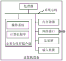
In one embodiment, a computer device is provided, the internal structure of which may be as shown in FIG. 7. The computer device includes a processor, a memory, a network interface, a display screen, and an input device connected by a system bus. Wherein the processor of the computer device is configured to provide computing and control capabilities. The memory of the computer device comprises a nonvolatile storage medium and an internal memory. The non-volatile storage medium stores an operating system and a computer program. The internal memory provides an environment for the operation of an operating system and computer programs in the non-volatile storage medium. The network interface of the computer device is used for communicating with an external terminal through a network connection. The computer program is executed by a processor to implement a communication data processing method. The display screen of the computer equipment can be a liquid crystal display screen or an electronic ink display screen, and the input device of the computer equipment can be a touch layer covered on the display screen, a key, a track ball or a touch pad arranged on the shell of the computer equipment, an external keyboard, a touch pad or a mouse and the like.
Those skilled in the art will appreciate that the architecture shown in fig. 7 is merely a block diagram of some of the structures associated with the disclosed aspects and is not intended to limit the computing devices to which the disclosed aspects apply, as particular computing devices may include more or less components than those shown, or may combine certain components, or have a different arrangement of components.
In one embodiment, a computer device is provided, comprising a memory and a processor, the memory having a computer program stored therein, the processor implementing the following steps when executing the computer program:
controlling the first kernel to receive a first trigger instruction sent by the FPGA, and sending at least one group of communication data to a shared memory for storage according to the first trigger instruction;
and controlling the second kernel to receive a second trigger instruction sent by the FPGA, and processing the communication data on the shared memory according to the second trigger instruction.
In one embodiment, the processor, when executing the computer program, further performs the steps of:
performing processing operations, the processing operations comprising: controlling the second kernel to acquire a data processing completion identifier on the shared memory, and determining a corresponding target address according to the data processing completion identifier; and controlling the second kernel to process the target communication data on the target address on the shared memory, and clearing the target address after the processing is finished.
In one embodiment, the processor, when executing the computer program, further performs the steps of:
and controlling the second kernel to judge whether the shared memory has a data processing completion identifier, and if so, returning to execute the processing operation until the data processing completion identifier does not exist in the shared memory.
In one embodiment, the processor, when executing the computer program, further performs the steps of:
controlling the second kernel to acquire the data processing completion identifier on the inter-kernel memory, and determining the target address according to the data processing completion identifier; the target address is used for storing target communication short data, a transmission identifier and an address of target communication long data, and the transmission identifier is used for representing whether the target communication data are stored in an inter-core memory and an external memory in a distributed mode;
controlling the second kernel to determine whether the target communication data is stored in the inter-kernel memory and the external memory in a distributed manner according to the transmission identifier on the target address in the inter-kernel memory;
and if so, controlling the second kernel to acquire target communication long data on the external memory.
In one embodiment, the processor, when executing the computer program, further performs the steps of:
controlling the second kernel to acquire the address of the target communication long data on the target address on the inter-kernel memory;
and controlling the second kernel to acquire the corresponding target communication long data on the external memory according to the address of the target communication long data.
In one embodiment, the processor, when executing the computer program, further performs the steps of:
controlling the second kernel to process the target communication short data, and clearing the address of the target communication short data in the inter-kernel memory after the processing is finished;
and if the target communication data is stored in the inter-core memory and the external memory in a distributed manner, controlling the second core to process the target communication long data, and clearing the address of the target communication long data in the external memory after the processing is finished.
In one embodiment, the processor, when executing the computer program, further performs the steps of:
and if the target communication data is stored in the inter-core memory, controlling the second core to process the target communication short data, and clearing the address of the target communication short data in the inter-core memory after the processing is finished.
In one embodiment, the trigger mechanism of the first trigger instruction and the trigger mechanism of the second trigger instruction are different, and the trigger mechanism is used for characterizing the interrupt frequency of the kernel.
In one embodiment, the processor, when executing the computer program, further performs the steps of:
and setting a plurality of pipeline state machines which are respectively used for recording the processing states of the services of the first kernel and the second kernel.
In one embodiment, a readable storage medium is provided, having stored thereon a computer program which, when executed by a processor, performs the steps of:
controlling the first kernel to receive a first trigger instruction sent by the FPGA, and sending at least one group of communication data to a shared memory for storage according to the first trigger instruction;
and controlling the second kernel to receive a second trigger instruction sent by the FPGA, and processing the communication data on the shared memory according to the second trigger instruction.
In one embodiment, the computer program when executed by the processor further performs the steps of:
performing processing operations, the processing operations comprising: controlling the second kernel to acquire a data processing completion identifier on the shared memory, and determining a corresponding target address according to the data processing completion identifier; and controlling the second kernel to process the target communication data on the target address on the shared memory, and clearing the target address after the processing is finished.
In one embodiment, the computer program when executed by the processor further performs the steps of:
and controlling the second kernel to judge whether the shared memory has a data processing completion identifier, and if so, returning to execute the processing operation until the data processing completion identifier does not exist in the shared memory.
In one embodiment, the computer program when executed by the processor further performs the steps of:
controlling the second kernel to acquire the data processing completion identifier on the inter-kernel memory, and determining the target address according to the data processing completion identifier; the target address is used for storing target communication short data, a transmission identifier and an address of target communication long data, and the transmission identifier is used for representing whether the target communication data are stored in an inter-core memory and an external memory in a distributed mode;
controlling the second kernel to determine whether the target communication data is stored in the inter-kernel memory and the external memory in a distributed manner according to the transmission identifier on the target address in the inter-kernel memory;
and if so, controlling the second kernel to acquire target communication long data on the external memory.
In one embodiment, the computer program when executed by the processor further performs the steps of:
controlling the second kernel to acquire the address of the target communication long data on the target address on the inter-kernel memory;
and controlling the second kernel to acquire the corresponding target communication long data on the external memory according to the address of the target communication long data.
In one embodiment, the computer program when executed by the processor further performs the steps of:
controlling the second kernel to process the target communication short data, and clearing the address of the target communication short data in the inter-kernel memory after the processing is finished;
and if the target communication data is stored in the inter-core memory and the external memory in a distributed manner, controlling the second core to process the target communication long data, and clearing the address of the target communication long data in the external memory after the processing is finished.
In one embodiment, the computer program when executed by the processor further performs the steps of:
and if the target communication data is stored in the inter-core memory, controlling the second core to process the target communication short data, and clearing the address of the target communication short data in the inter-core memory after the processing is finished.
In one embodiment, the trigger mechanism of the first trigger instruction and the trigger mechanism of the second trigger instruction are different, and the trigger mechanism is used for characterizing the interrupt frequency of the kernel.
In one embodiment, the computer program when executed by the processor further performs the steps of:
and setting a plurality of pipeline state machines which are respectively used for recording the processing states of the services of the first kernel and the second kernel.
It will be understood by those skilled in the art that all or part of the processes of the methods of the embodiments described above can be implemented by hardware instructions of a computer program, which can be stored in a non-volatile computer-readable storage medium, and when executed, can include the processes of the embodiments of the methods described above. Any reference to memory, storage, database, or other medium used in the embodiments provided herein may include non-volatile and/or volatile memory, among others. Non-volatile memory can include read-only memory (ROM), Programmable ROM (PROM), Electrically Programmable ROM (EPROM), Electrically Erasable Programmable ROM (EEPROM), or flash memory. Volatile memory can include Random Access Memory (RAM) or external cache memory. By way of illustration and not limitation, RAM is available in a variety of forms such as Static RAM (SRAM), Dynamic RAM (DRAM), Synchronous DRAM (SDRAM), Double Data Rate SDRAM (DDRSDRAM), Enhanced SDRAM (ESDRAM), Synchronous Link DRAM (SLDRAM), Rambus Direct RAM (RDRAM), direct bus dynamic RAM (DRDRAM), and memory bus dynamic RAM (RDRAM).
The technical features of the above embodiments can be arbitrarily combined, and for the sake of brevity, all possible combinations of the technical features in the above embodiments are not described, but should be considered as the scope of the present specification as long as there is no contradiction between the combinations of the technical features.
The above-mentioned embodiments only express several embodiments of the present application, and the description thereof is more specific and detailed, but not construed as limiting the scope of the invention. It should be noted that, for a person skilled in the art, several variations and modifications can be made without departing from the concept of the present application, which falls within the scope of protection of the present application. Therefore, the protection scope of the present patent shall be subject to the appended claims.
Claims (13)
1. A communication data processing method is applied to a communication data processing system, wherein the communication data processing system comprises a first kernel, a second kernel, a shared memory and an FPGA, and the method comprises the following steps:
controlling the first kernel to receive a first trigger instruction sent by the FPGA, and sending at least one group of communication data to a shared memory for storage according to the first trigger instruction;
and controlling the second kernel to receive a second trigger instruction sent by the FPGA, and processing the communication data on the shared memory according to the second trigger instruction.
2. The method of claim 1, wherein the processing the communication data on the shared memory comprises:
performing processing operations, the processing operations comprising: controlling the second kernel to acquire a data processing completion identifier on the shared memory, and determining a corresponding target address according to the data processing completion identifier; and controlling the second kernel to process the target communication data on the target address on the shared memory, and clearing the target address after the processing is finished.
3. The method of claim 2, further comprising:
and controlling the second kernel to judge whether the shared memory has a data processing completion identifier, and if so, returning to execute the processing operation until the data processing completion identifier does not exist in the shared memory.
4. The method according to claim 2 or 3, wherein the target communication data comprises target communication short data and target communication long data, and the shared memory comprises an inter-core memory and an external memory;
the controlling the second kernel to obtain a data processing completion identifier on the shared memory, and determining a corresponding target address according to the data processing completion identifier includes:
controlling the second kernel to acquire the data processing completion identifier on the inter-kernel memory, and determining the target address according to the data processing completion identifier; the target address is used for storing target communication short data, a transmission identifier and an address of target communication long data, and the transmission identifier is used for representing whether the target communication data are stored in an inter-core memory and an external memory in a distributed mode;
controlling the second kernel to determine whether the target communication data is stored in the inter-kernel memory and the external memory in a distributed manner according to the transmission identifier on the target address in the inter-kernel memory;
and if so, controlling the second kernel to acquire target communication long data on the external memory.
5. The method according to claim 4, wherein the controlling the second kernel to obtain target communication long data on the external memory comprises:
controlling the second kernel to acquire the address of the target communication long data on the target address on the inter-kernel memory;
and controlling the second kernel to acquire the corresponding target communication long data on the external memory according to the address of the target communication long data.
6. The method according to claim 4, wherein the controlling the second kernel to process the target communication data at the target address on the shared memory and to flush the target address after the processing is completed comprises:
controlling the second kernel to process the target communication short data, and clearing the address of the target communication short data in the inter-kernel memory after the processing is finished;
and if the target communication data is stored in the inter-core memory and the external memory in a distributed manner, controlling the second core to process the target communication long data, and clearing the address of the target communication long data in the external memory after the processing is finished.
7. The method according to claim 4, wherein the controlling the second kernel to process the target communication data at the target address on the shared memory and to flush the target address after the processing is completed comprises:
and if the target communication data is stored in the inter-core memory, controlling the second core to process the target communication short data, and clearing the address of the target communication short data in the inter-core memory after the processing is finished.
8. The method of claim 1, wherein the first trigger instruction and the second trigger instruction have different trigger mechanisms, and wherein the trigger mechanisms are used to characterize interrupt frequency of the core.
9. The method of claim 1, further comprising:
and setting a plurality of pipeline state machines which are respectively used for recording the processing states of the services of the first kernel and the second kernel.
10. A communication data processing device is applied to a communication data processing system, wherein the communication data processing system comprises a first kernel, a second kernel, a shared memory and an FPGA, and the device comprises:
the first control module is used for controlling the first kernel to receive a first trigger instruction sent by the FPGA and sending at least one group of communication data to the shared memory for storage according to the first trigger instruction;
and the second control module is used for controlling the second kernel to receive a second trigger instruction sent by the FPGA and processing the communication data on the shared memory according to the second trigger instruction.
11. An apparatus comprising a memory and a processor, the memory storing a computer program, wherein the processor implements the steps of the method of any one of claims 1 to 9 when executing the computer program.
12. A communication data processing system comprises a shared memory, an FPGA, a first kernel and a second kernel, and is characterized in that,
the first kernel is used for receiving a first trigger instruction sent by the FPGA and sending at least one group of communication data to the shared memory for storage;
the second kernel is used for receiving a second trigger instruction sent by the FPGA and processing the communication data on the shared memory;
and the FPGA is used for sending a first trigger instruction to the first kernel and sending a second trigger instruction to the second kernel.
13. A readable storage medium, on which a computer program is stored, which, when being executed by a processor, carries out the steps of the method of any one of claims 1 to 9.
Priority Applications (1)
| Application Number | Priority Date | Filing Date | Title |
|---|---|---|---|
| CN201911420234.0A CN111190854B (en) | 2019-12-31 | 2019-12-31 | Communication data processing method, device, equipment, system and storage medium |
Applications Claiming Priority (1)
| Application Number | Priority Date | Filing Date | Title |
|---|---|---|---|
| CN201911420234.0A CN111190854B (en) | 2019-12-31 | 2019-12-31 | Communication data processing method, device, equipment, system and storage medium |
Publications (2)
| Publication Number | Publication Date |
|---|---|
| CN111190854A true CN111190854A (en) | 2020-05-22 |
| CN111190854B CN111190854B (en) | 2024-03-26 |
Family
ID=70707978
Family Applications (1)
| Application Number | Title | Priority Date | Filing Date |
|---|---|---|---|
| CN201911420234.0A Active CN111190854B (en) | 2019-12-31 | 2019-12-31 | Communication data processing method, device, equipment, system and storage medium |
Country Status (1)
| Country | Link |
|---|---|
| CN (1) | CN111190854B (en) |
Cited By (5)
| Publication number | Priority date | Publication date | Assignee | Title |
|---|---|---|---|---|
| CN112799814A (en) * | 2021-01-28 | 2021-05-14 | 中国科学院地质与地球物理研究所 | Dual-core seismic intensity meter and task scheduling method |
| CN112988427A (en) * | 2021-04-14 | 2021-06-18 | 深圳证券交易所 | Data exchange method, device and medium |
| CN114167845A (en) * | 2021-12-23 | 2022-03-11 | 广东嘉腾机器人自动化有限公司 | Communication offline diagnosis method and system for PLC and equipment |
| CN114228725A (en) * | 2021-11-23 | 2022-03-25 | 深圳元戎启行科技有限公司 | Vehicle-mounted control system and unmanned vehicle |
| CN114338515A (en) * | 2021-12-09 | 2022-04-12 | 中汽创智科技有限公司 | Data transmission method, device, equipment and storage medium |
Citations (4)
| Publication number | Priority date | Publication date | Assignee | Title |
|---|---|---|---|---|
| CN102270189A (en) * | 2011-06-17 | 2011-12-07 | 西安电子科技大学 | Inter-core communication method based on FPGA (Field Programmable Gate Array) multi-core system |
| CN105431827A (en) * | 2013-08-07 | 2016-03-23 | 高通股份有限公司 | Dynamic address negotiation for shared memory regions in heterogeneous muliprocessor systems |
| CN109254860A (en) * | 2018-09-28 | 2019-01-22 | 中国科学院长春光学精密机械与物理研究所 | A kind of data processing system and terminal device of heterogeneous polynuclear platform |
| CN110545319A (en) * | 2019-08-23 | 2019-12-06 | 武汉久同智能科技有限公司 | design of SoC core system and method for realizing task communication between cores |
-
2019
- 2019-12-31 CN CN201911420234.0A patent/CN111190854B/en active Active
Patent Citations (4)
| Publication number | Priority date | Publication date | Assignee | Title |
|---|---|---|---|---|
| CN102270189A (en) * | 2011-06-17 | 2011-12-07 | 西安电子科技大学 | Inter-core communication method based on FPGA (Field Programmable Gate Array) multi-core system |
| CN105431827A (en) * | 2013-08-07 | 2016-03-23 | 高通股份有限公司 | Dynamic address negotiation for shared memory regions in heterogeneous muliprocessor systems |
| CN109254860A (en) * | 2018-09-28 | 2019-01-22 | 中国科学院长春光学精密机械与物理研究所 | A kind of data processing system and terminal device of heterogeneous polynuclear platform |
| CN110545319A (en) * | 2019-08-23 | 2019-12-06 | 武汉久同智能科技有限公司 | design of SoC core system and method for realizing task communication between cores |
Cited By (8)
| Publication number | Priority date | Publication date | Assignee | Title |
|---|---|---|---|---|
| CN112799814A (en) * | 2021-01-28 | 2021-05-14 | 中国科学院地质与地球物理研究所 | Dual-core seismic intensity meter and task scheduling method |
| CN112988427A (en) * | 2021-04-14 | 2021-06-18 | 深圳证券交易所 | Data exchange method, device and medium |
| CN112988427B (en) * | 2021-04-14 | 2024-03-01 | 深圳证券交易所 | Data exchange method, device and medium |
| CN114228725A (en) * | 2021-11-23 | 2022-03-25 | 深圳元戎启行科技有限公司 | Vehicle-mounted control system and unmanned vehicle |
| CN114338515A (en) * | 2021-12-09 | 2022-04-12 | 中汽创智科技有限公司 | Data transmission method, device, equipment and storage medium |
| CN114338515B (en) * | 2021-12-09 | 2023-08-22 | 中汽创智科技有限公司 | Data transmission method, device, equipment and storage medium |
| CN114167845A (en) * | 2021-12-23 | 2022-03-11 | 广东嘉腾机器人自动化有限公司 | Communication offline diagnosis method and system for PLC and equipment |
| CN114167845B (en) * | 2021-12-23 | 2023-12-05 | 广东嘉腾机器人自动化有限公司 | Communication offline diagnosis method and system for PLC and equipment |
Also Published As
| Publication number | Publication date |
|---|---|
| CN111190854B (en) | 2024-03-26 |
Similar Documents
| Publication | Publication Date | Title |
|---|---|---|
| CN111190854A (en) | Communication data processing method, device, equipment, system and storage medium | |
| CN108628684B (en) | DPDK-based message processing method and computer equipment | |
| US20200174669A1 (en) | Management method and apparatus for multi-system shared memory | |
| CN113918101B (en) | Method, system, equipment and storage medium for writing data cache | |
| CN109450701B (en) | Virtual switch switching method and device, host machine and computer readable storage medium | |
| CN110532205B (en) | Data transmission method, data transmission device, computer equipment and computer readable storage medium | |
| CN114595186B (en) | Inter-core communication method and communication device of multi-core processor | |
| CN115964319A (en) | Data processing method for remote direct memory access and related product | |
| CN113535425A (en) | Data sending method and device, electronic equipment and storage medium | |
| CN103823712A (en) | Data flow processing method and device for multi-CPU virtual machine system | |
| KR102303424B1 (en) | Direct memory access control device for at least one processing unit having a random access memory | |
| CN110597643B (en) | Inter-core communication method, processor and electronic equipment | |
| US20230342086A1 (en) | Data processing apparatus and method, and related device | |
| CN112506676A (en) | Inter-process data transmission method, computer device and storage medium | |
| CN102117261B (en) | Communication method between inner processors of chip | |
| CN116155992A (en) | Method and device for subscribing resources | |
| CN113037649B (en) | Method and device for transmitting and receiving network interrupt data packet, electronic equipment and storage medium | |
| CN104811391B (en) | Data packet processing method and device and server | |
| CN115220993A (en) | Process monitoring method, device, vehicle and storage medium | |
| CN113204517A (en) | Inter-core sharing method of Ethernet controller special for electric power | |
| US20190050253A1 (en) | Memory register interrupt based signaling and messaging | |
| US10664407B2 (en) | Dual first and second pointer for memory mapped interface communication with lower indicating process | |
| WO2021102849A1 (en) | Resource acquisition method and apparatus, and electronic device | |
| CN110955461A (en) | Processing method, device and system of computing task, server and storage medium | |
| CN115878351B (en) | Message transmission method and device, storage medium and electronic device |
Legal Events
| Date | Code | Title | Description |
|---|---|---|---|
| PB01 | Publication | ||
| PB01 | Publication | ||
| SE01 | Entry into force of request for substantive examination | ||
| SE01 | Entry into force of request for substantive examination | ||
| CB02 | Change of applicant information |
Address after: 510663 Shenzhou Road 10, Guangzhou Science City, Guangzhou economic and Technological Development Zone, Guangzhou, Guangdong Applicant after: Jingxin Network System Co.,Ltd. Address before: 510663 Shenzhou Road 10, Guangzhou Science City, Guangzhou economic and Technological Development Zone, Guangzhou, Guangdong Applicant before: COMBA TELECOM SYSTEMS (CHINA) Ltd. |
|
| CB02 | Change of applicant information | ||
| GR01 | Patent grant | ||
| GR01 | Patent grant |