The method for preparing semiconductor device
Technical field
The present invention relates to semiconductor device, specifically, relate to the method that preparation has the semiconductor device of capacitor, for example DRAM (dynamic RAM).
Background of invention
By making the memory cell microminiaturization, the DRAM that constitutes its memory by a triode and capacitor is integrated to heavens.
Along with the minimizing of memory unit area, the area that capacitor occupies also reduces thereupon, therefore, is difficult to obtain the required charge storage capacity of soft error impedance (soft error resistance) (approximately 25fF).
Now, the storage electrode that is called stack type (stack type) is widely used, form small hemisphere silicon wafer particle on the storage electrode surface, promptly HSG-Si (hemi-spherical granule silicon) also is applied so that increase the technology of the effective surface area of electrode.
By in amorphous state-crystalline state transformetion range, annealing in process being carried out on the amorphous silicon membrane surface of cleaning, make on the amorphous silicon membrane surface and form nucleus, utilize the surface migration effect of silicon atom to make nucleus growth then, and then finished the preparation process of HSG-Si.
Therefore, to require amorphous silicon membrane surface as parent be a cleaning, do not have the surface of spontaneous oxide layer and organic impurities, and also requiring the anneal environment of preparation HSG-Si is high vacuum environment or non-oxidizing atmosphere.
In addition, silicon metal surface ratio amorphous silicon surfaces is more stable, and on the silicon metal surface, the surface migration phenomenon of rare silicon atom is not so can form any HSG-Si.Therefore, the surface of formation HSG-Si must be the amorphous silicon surface.
According to the principle that film generates, the technology that generates HSG-Si can be divided into selectivity HSG method and shelter formula HSG method, and these methods have following merits and demerits respectively.
In selectivity HSG method, HSG optionally only is formed on the surface of storage electrode of previous formation, after film forms, compares with sheltering formula HSG method, no longer needs the deep etch step.Therefore, selectivity HSG method has the less advantage of operating procedure.
Japanese patent application Laid-open has introduced a kind of method No. 315543/1993, and this method comprises utilizes selectivity HSG method to form the storage electrode figure, and deposition of amorphous silicon is carried out deep etch electrode is separated from each other, and forms HSG-Si at last.
In addition, in selectivity HSG method, the shape of storage electrode is not subjected to the restriction of deep etch step, and therefore, selectivity HSG method has the advantage that can be used to prepare the complicated shape storage electrode, for example cylindricality or fin-shaped.
Yet, utilize the process of selectivity HSG method formation HSG responsive especially to the state of electrode surface, particularly,, be easy to occur can not forming the problem of any HSG owing to the existence and the organic pollution of spontaneous oxide layer.
In contrast, in sheltering formula HSG method, show that HSG is integrally formed as its name.At first, integrally form amorphous silicon membrane, then, under the condition that amorphous silicon membrane is not exposed in the environment, anneal, so that form HSG as parent.
Therefore, shelter formula HSG method and have the advantage that can not produce any spontaneous oxide layer and not be subjected to any organic pollutants.Yet, owing to formed whole film, need utilize some technology, for example deep etch technology is isolated from each other storage electrode, and the shape of electrode is subjected to the restriction of deep etch step.
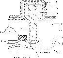
Below, main according to sheltering formula HSG method, to Fig. 3 (e), traditional technology is described with reference to Fig. 3 (a).
At first, shown in Fig. 3 (a), in the drain electrode 2 of the Semiconductor substrate that contains MOS-FET etc., prepare contact hole, then, utilize known vacuum chemistry vapor phase growth method, form amorphous, contain first silicon thin film 9 of phosphorus as impurity.
Then, shown in Fig. 3 (b), utilize known photoetching technique, first silicon thin film 9 is made the shape of expection, so that form the part storage electrode.In Fig. 3 (b), only show single storage electrode, and in fact, the shape of storage electrode is a dumb-bell shape.
After this, utilize the hydrofluoric acid or the similar solution of dilution, remove the spontaneous oxide layer on first silicon thin film 9, shown in Fig. 3 (c), utilize the vacuum chemistry vapor phase growth method, by containing silane (SiH
4) or disilane (Si
2H
6) gas system integrally form second silicon thin film 15.At this moment, the formation condition of film guarantees that second silicon thin film 15 is in amorphous state.
Correspondingly, carry out annealing in process in airborne high vacuum environment or the non-oxidizing atmosphere second silicon thin film 15 not being exposed to, 13 beginnings of hemisphere silicon wafer particle are grown, on the surface of the broad film 15 of second silicon shown in Fig. 3 (d).
Once more, utilize known anisotropic dry etching technology to carry out deep etch, storage electrode is isolated from each other, shown in Fig. 3 (e).
Then, form dielectric film and plate electrode, and then prepare capacitor.
It is insensitive to lip-deep spontaneous oxide layer of storage electrode and organic pollution to shelter formula HSG method, and it has very wide tolerance limit.Thus, sheltering formula HSG method is good method.
Yet, in sheltering formula HSG method, along with the increase of the film thickness of first silicon thin film 9, the problem that the storage electrode part does not change HSG or growth size deficiency into will take place.
The storage electrode that does not change HSG into lacks capacitance, and therefore, its shortcoming is impossible carry out normal running and the position takes place losing efficacy.
According to the result of investigation, illustrated part first silicon thin film 8 crystallization has taken place, therefore, before growth HSG-Si, crystallization also takes place in second silicon thin film 15.As discussed above, on crystal surface, can not generate any HSG-Si.
The incidence that lost efficacy is to have prolonged thermal history owing to having prolonged surperficial formation time with the reason that the thickness of first silicon thin film 9 increases, and therefore, is easy to form nucleus between film inside or film and end liner.
Be appreciated that the growth rate owing to crystal in the film is higher than the formation speed of amorphous silicon, the crystallization phenomenon will arrive the surface.
In traditional technology, think that it is important being electrically connected, therefore, after removing the lip-deep spontaneous oxide layer of storage electrode, form second silicon thin film 15.Therefore, as shown in Figure 4, can suppose that when the first silicon thin film generation crystallization, this fact also will make 15 crystallizations of second silicon thin film.
Therefore, before forming second silicon thin film 15, by utilizing the mixed solution treatment surface of ammoniacal liquor and hydrogenperoxide steam generator, make of the influence of fine and close spontaneous oxide layer covering surfaces to avoid first silicon thin film, 9 crystallizations to produce, can reduce the inefficacy that does not obtain HSG and so on significantly.
On the other hand, also exist the problem of the impurity number deficiency among another HSG that is incorporated into formation, therefore, because depletion effect, electric empty amount can not as was expected increases significantly.
Only otherwise the HSG that forms is carried out any processing, it does not just comprise any impurity.Therefore, should use certain device that impurity is introduced wherein.
In conventional art, impurity in first silicon thin film 9 through 15 thermal diffusions of second silicon thin film in HSG-Si, but, clearly, the spontaneous oxide layer that formed before second silicon thin film 15 forms has played the effect of diffusion of impurities potential barrier or diffusion of impurities trap, therefore, be incorporated into the amount of impurities deficiency of HSG-Si.
Therefore,, attempting in second silicon thin film 15, adding impurity, forming HSG-Si then for the ease of impurity is drawn HSG-Si.Yet in this case, the growth rate of HSG-S is very low, can not obtain enough big HSG-Si.Fig. 5 example the relation between the particle size of 565 ℃ of following annealing times and HSG-Si.
When HSG-Si for example be resized to 70nm the time, for doping content is 2.03E20[atoms/cc] doped amorphous silicon (among Fig. 5 with " about 50 minutes annealing time; although for non-doped amorphous silicon the curve of (among the Fig. 5 with " ") only needs 5 minutes annealing time.
Contain in the amorphous silicon membrane as parent under the situation of phosphorus as impurity, the surface migration effect of silicon atom is by the decision of subduing of phosphorus, and impurity concentration is high more, and the growth rate of HSG-Si is just low more.
In contrast, when impurity concentration was very high, the growth of crystal was more prone in the film, if the crystal in second silicon thin film 15 began growth before HSG-Si grows fully, and arrived the surface, and the growth of HSG-Si will stop.Therefore, only can not obtain bigger particle by prolonging annealing time.
As mentioned above, utilize conventional art, be difficult in the HSG-Si that suppresses to cause and grow when failing, the impurity of capacity is introduced HSG-Si, obtain high capacity owing to crystallization.
Summary of the invention
The purpose of this invention is to provide a kind of method for preparing semiconductor device, this method does not have above-mentioned problem, and can prevent the HSG-Si growth failure that accompanying crystallization produces, also be easy to control the growth rate of HSG-Si, the impurity of capacity HSG-Si can be introduced, the electric capacity degeneration that depletion effect causes can be overcome.
Utilize following the present invention can realize above-mentioned purpose.
That is to say, the invention discloses the method that preparation has the semiconductor device of capacitor, wherein capacitor has upper electrode, dielectric film and lower electrode, wherein lower electrode forms by following steps: form the step of first silicon thin film, this silicon thin film comprises impurity and the method by the vacuum chemistry vapour growth and is grown on the first type surface of Semiconductor substrate with the form of amorphous state or polycrystalline attitude; First silicon thin film is made the step of reservation shape; Form the step of spontaneous oxide layer at first silicon film surface; Form the step of second silicon thin film, this silicon thin film contains impurity and grows with amorphous form by the method for vacuum chemistry vapour growth; Form the step of the 3rd silicon thin film, the free from foreign meter and method by the vacuum chemistry vapour growth of this silicon thin film will not be exposed to a part under the airborne condition, with amorphous form growth; Not being exposed to the step of in the airborne non-oxidizing atmosphere the 3rd silicon thin film being carried out annealing in process with a part, make the 3rd silicon thin film crystallization, therefore form hemisphere silicon wafer particle; With utilize anisotropic lithographic technique to carry out the step of deep etch.The semiconductor device that utilizes this manufacture method to obtain is also disclosed.
The method of making semiconductor device of the present invention is the method that a kind of preparation has the semiconductor device of capacitor, capacitor has upper electrode, dielectric film and lower electrode, wherein lower electrode forms by following steps: form the step of first silicon thin film, this silicon thin film comprises impurity and the method by the vacuum chemistry vapour growth and is grown on the first type surface of Semiconductor substrate with the form of amorphous state or polycrystalline attitude; First silicon thin film is made the step of reservation shape: the step that forms spontaneous oxide layer at first silicon film surface; Form the step of second silicon thin film, this silicon thin film contains impurity and grows with amorphous form by the method for vacuum chemistry vapour growth; Form the step of the 3rd silicon thin film, the free from foreign meter and method by the vacuum chemistry vapour growth of this silicon thin film will not be exposed to a part under the airborne condition, with amorphous form growth; Not being exposed to the step of in the airborne non-oxidizing atmosphere the 3rd silicon thin film being carried out annealing in process with a part, make the 3rd silicon thin film crystallization, therefore form hemisphere silicon wafer particle; With utilize anisotropic lithographic technique to carry out the step of deep etch.
The method for preparing semiconductor device of the present invention is characterised in that the spontaneous thickness of oxide layer on first silicon film surface is 2nm or littler, the impurity that the feature for preparing the method for semiconductor device of the present invention also is to introduce second silicon thin film is phosphorus, and the concentration range of phosphorus is that 1E20 is to 3E20[atoms/cc].
In addition, prepare thickness that the method for semiconductor device of the present invention is characterised in that second silicon thin film between 10 to 70nm, the feature for preparing the method for semiconductor device of the present invention is that also the thickness of the 3rd silicon thin film is between 5 to 60nm.
Description of drawings
Fig. 1 is the description of the process figure about the present invention's first and second embodiments.
Fig. 2 is the section sketch map about the present invention's first and second embodiments.
Fig. 3 is the description of the process figure about conventional art.
Fig. 4 is the section sketch map of the HSG-Si growth failure that shown that conventional art causes.
Fig. 5 is the particle size of HSG-Si and the relation curve between the annealing time.
Embodiment
In these accompanying drawings, 1 expression Semiconductor substrate, 2 expression drain electrodes, 3 expression source electrodes, 4 expression grids, 5 expression field oxides, 6 expressions, first interlayer insulating film, 7 expression bit lines (bitline), 8 expressions, second interlayer insulating film, 9a represents first silicon thin film of crystallization, the spontaneous oxide film of 10 expressions, 11 expression second silicon thin films (the present invention), 12 expression the 3rd silicon thin films (the present invention), 12a represents second silicon thin film (conventional art) of crystallization, 13 expression hemisphere silicon wafer particles (HSG-Si), the heterogeneity that 14 expression deep etch produce, 15 expression second silicon thin films (conventional art).
Below, with reference to accompanying drawing, describe the present invention in detail, but scope of the present invention is not subjected to the restriction of these examples according to various examples.
Example 1
First embodiment of the present invention is described with reference to Fig. 1 (a) to Fig. 1 (e).At first, shown in Fig. 1 (a), in the drain electrode 2 of the Semiconductor substrate that contains MOS-FET etc., prepare contact hole, then, utilize known vacuum chemistry vapor phase growth method, form amorphous, contain first silicon thin film 9 of phosphorus as impurity.
Then, shown in Fig. 1 (b), utilize known photoetching technique, first silicon thin film 9 is made the shape of expection, so that form the part storage electrode.Sequential operation till this step is identical with conventional art.
After this, substrate was soaked 3 minutes in 60 ℃ mixed solution of ammoniacal liquor and hydrofluoric acid composition, remove particle, form fine and close spontaneous oxide layer 10 simultaneously on the surface of first silicon thin film 9.
In this embodiment, adopted ammoniacal liquor-hydrofluoric acid (APM flushing) technology, but can also adopt any other method, for example utilized sulfuric acid-hydrofluoric acid (SPM flushing), as long as can form the thick dense oxidation film of about 2nm.These methods are purging methods very common in the semiconductor preparing process.
Spontaneous oxide layer should sufficiently approach, so that realize being electrically connected by tunnel current without a doubt.Another kind method, for example low-temperature oxidation or rapid thermal oxidation can form thermal oxide layer as thin as a wafer, still, if bed thickness surpasses 3nm, just can not ignore the impedance of oxide layer self again.Therefore, should note the thickness of film more.
Utilize fine and close spontaneous oxide layer in this way to cover first silicon thin film 9, as shown in Figure 2, second silicon thin film 11 and the 3rd silicon thin film 12 that form in turn will be protected, and avoid the crystallization that causes by as the crystal that produces in first silicon thin film 9 of end liner.
Then, shown in Fig. 1 (c), utilize the vacuum chemistry vapor phase growth method, by containing silane (SiH
4) or disilane (Si
2H
6) gas system form and to contain second silicon thin film 11 of phosphorus as impurity.
Phosphorus concentration in the film is at 1.0E20 to 3.0E20[atoms/cc] between.If concentration is less than this scope, then the phosphorus deficiency of introducing at HSG-Si if surpass this scope, then is easy to generate crystallization in film.
The thickness of second silicon thin film 11 is greatly about between the 10nm to 70nm.If the thickness of second silicon thin film 11 is less than 10nm, in heating steps subsequently, be difficult to diffusion of impurities with capacity so in HSG-Si.
Then, sequentially form the 3rd silicon thin film 12, its thickness is greatly about between the 5nm to 60nm, by containing silane (SiH
4) or disilane (Si
2H
6) gas system form will not being exposed under the airborne condition with a part.
If the thickness of the 3rd silicon thin film 12 is less than 5nm, in subsequent annealing step, because the growth of HSG-Si, the 3rd silicon thin film 12 will be depleted soon, thus, can not obtain the HSG of sufficient size so.If thickness surpasses 60nm, then be difficult to from the second silicon thin film thermal diffusion impurity.
The film formation condition of second silicon thin film 11 and the 3rd silicon thin film 12 should guarantee that they all are in amorphous state, and when the film formation temperature is between 530 to 590 ℃, film forms pressure between 0.2 to 80 Torr time, and it is possible forming this amorphous state.Usually, form under the pressure conditions of higher than low and film, be easy to generate amorphous state in the film formation temperature.
Contain second silicon thin film 11 of impurity and the 3rd silicon thin film 12 free from foreign meter by in this way forming, in follow-up step, the impurity of capacity can be introduced HSG, and can not reduce the growth rate of HSG, the HSG growth failure that crystallization causes can be prevented simultaneously, and the problem that exhausts the capacitance degeneration that causes can be solved.
Next step stops air feed, then, near amorphous state-crystalline state transition temperature, not being exposed under the airborne condition, carries out annealing in process, forms HSG-Si, shown in Fig. 1 (d).
Annealing temperature is preferably between 550 to 580 ℃.Fig. 5 shown utilize thickness for 30nm, contain concentration and be 2.0E20[atoms/cc] phosphorus make second silicon thin film 11 as the amorphous silicon of impurity, utilize thickness to make for 20nm, undoped amorphous silicon under the condition of the 3rd silicon thin film 12, the relation between the particle size of annealing time and HSG-Si (curve of representing with A among Fig. 5).
When particle size during greater than 60nm, the reason that the growth rate of curve A descends suddenly is because the growth of HSG-Si and the 3rd silicon thin film is exhausted, and thus, second silicon thin film comes out.
At a crystallite dimension place of selecting, the growth rate of crystal grain can be lowered, if utilize this phenomenon, can control crystallite dimension (Fig. 1 (e) and Fig. 2 have shown a kind of the 3rd silicon thin film 12 remaining situations that also have respectively) at an easy rate.
Then, utilize anisotropic dry etching technology to carry out deep etch, storage electrode is isolated mutually, shown in Fig. 1 (e).
Next step forms dielectric film and plate electrode, makes the capacitor (not shown).
Here, dielectric film has sull-nitride film structure, by 850 ℃ of following high-temperature oxydations 20 minutes, and utilizes the vacuum chemistry vapor phase growth method to form part silicon nitrogen film surface, and forms this structure.By adding thermal history specifically, the impurity thermal diffusion is in HSG-Si.
Example 2
Second embodiment of the present invention is polycrystalline attitude first silicon thin film 9 among preparation Fig. 1 (a).In the present invention, shown in Fig. 1 (b), form second silicon thin film 11 (seeing Fig. 1 (c)) before, covering the surface of first silicon thin film 9 with fine and close spontaneous oxide layer 10.Therefore, even crystallization takes place first silicon thin film 9, this crystallization can not produce any influence to second silicon thin film 11 yet.
Therefore, after forming first silicon thin film and carving, pass through POCl with figure
3Thermal diffusion introduce phosphorus.
In this case, utilize hydrofluoric acid or similar solution after diluting to remove the phosphorus glass layer, in the mixed solution of sulfuric acid and hydrogen peroxide, soaked 5 minutes then, finally form spontaneous oxide layer.After this, utilize the processing procedure identical to form capacitor with the first above-mentioned embodiment.
According to the present invention, as mentioned above, first silicon film surface has covered fine and close spontaneous oxide film, the HSG-Si growth failure that therefore can avoid crystallization to cause.In addition, the amorphous silicon membrane that forms parent as HSG is divided into second silicon thin film and the 3rd silicon thin film that contains impurity, therefore, can control the speed of growth of HSG-Si at an easy rate, the impurity of capacity can be introduced HSG-Si, and can avoid exhausting the capacitor that causes and degenerate.