CN110095897B - Display device - Google Patents
Display device Download PDFInfo
- Publication number
- CN110095897B CN110095897B CN201910214418.5A CN201910214418A CN110095897B CN 110095897 B CN110095897 B CN 110095897B CN 201910214418 A CN201910214418 A CN 201910214418A CN 110095897 B CN110095897 B CN 110095897B
- Authority
- CN
- China
- Prior art keywords
- light
- light source
- display
- liquid crystal
- color
- Prior art date
- Legal status (The legal status is an assumption and is not a legal conclusion. Google has not performed a legal analysis and makes no representation as to the accuracy of the status listed.)
- Active
Links
Images


Classifications
-
- G—PHYSICS
- G02—OPTICS
- G02F—OPTICAL DEVICES OR ARRANGEMENTS FOR THE CONTROL OF LIGHT BY MODIFICATION OF THE OPTICAL PROPERTIES OF THE MEDIA OF THE ELEMENTS INVOLVED THEREIN; NON-LINEAR OPTICS; FREQUENCY-CHANGING OF LIGHT; OPTICAL LOGIC ELEMENTS; OPTICAL ANALOGUE/DIGITAL CONVERTERS
- G02F1/00—Devices or arrangements for the control of the intensity, colour, phase, polarisation or direction of light arriving from an independent light source, e.g. switching, gating or modulating; Non-linear optics
- G02F1/01—Devices or arrangements for the control of the intensity, colour, phase, polarisation or direction of light arriving from an independent light source, e.g. switching, gating or modulating; Non-linear optics for the control of the intensity, phase, polarisation or colour
- G02F1/13—Devices or arrangements for the control of the intensity, colour, phase, polarisation or direction of light arriving from an independent light source, e.g. switching, gating or modulating; Non-linear optics for the control of the intensity, phase, polarisation or colour based on liquid crystals, e.g. single liquid crystal display cells
- G02F1/133—Constructional arrangements; Operation of liquid crystal cells; Circuit arrangements
- G02F1/1333—Constructional arrangements; Manufacturing methods
- G02F1/1334—Constructional arrangements; Manufacturing methods based on polymer dispersed liquid crystals, e.g. microencapsulated liquid crystals
-
- G—PHYSICS
- G02—OPTICS
- G02F—OPTICAL DEVICES OR ARRANGEMENTS FOR THE CONTROL OF LIGHT BY MODIFICATION OF THE OPTICAL PROPERTIES OF THE MEDIA OF THE ELEMENTS INVOLVED THEREIN; NON-LINEAR OPTICS; FREQUENCY-CHANGING OF LIGHT; OPTICAL LOGIC ELEMENTS; OPTICAL ANALOGUE/DIGITAL CONVERTERS
- G02F1/00—Devices or arrangements for the control of the intensity, colour, phase, polarisation or direction of light arriving from an independent light source, e.g. switching, gating or modulating; Non-linear optics
- G02F1/01—Devices or arrangements for the control of the intensity, colour, phase, polarisation or direction of light arriving from an independent light source, e.g. switching, gating or modulating; Non-linear optics for the control of the intensity, phase, polarisation or colour
- G02F1/13—Devices or arrangements for the control of the intensity, colour, phase, polarisation or direction of light arriving from an independent light source, e.g. switching, gating or modulating; Non-linear optics for the control of the intensity, phase, polarisation or colour based on liquid crystals, e.g. single liquid crystal display cells
- G02F1/133—Constructional arrangements; Operation of liquid crystal cells; Circuit arrangements
- G02F1/1333—Constructional arrangements; Manufacturing methods
- G02F1/1335—Structural association of cells with optical devices, e.g. polarisers or reflectors
- G02F1/1336—Illuminating devices
- G02F1/133615—Edge-illuminating devices, i.e. illuminating from the side
-
- G—PHYSICS
- G02—OPTICS
- G02F—OPTICAL DEVICES OR ARRANGEMENTS FOR THE CONTROL OF LIGHT BY MODIFICATION OF THE OPTICAL PROPERTIES OF THE MEDIA OF THE ELEMENTS INVOLVED THEREIN; NON-LINEAR OPTICS; FREQUENCY-CHANGING OF LIGHT; OPTICAL LOGIC ELEMENTS; OPTICAL ANALOGUE/DIGITAL CONVERTERS
- G02F1/00—Devices or arrangements for the control of the intensity, colour, phase, polarisation or direction of light arriving from an independent light source, e.g. switching, gating or modulating; Non-linear optics
- G02F1/01—Devices or arrangements for the control of the intensity, colour, phase, polarisation or direction of light arriving from an independent light source, e.g. switching, gating or modulating; Non-linear optics for the control of the intensity, phase, polarisation or colour
- G02F1/13—Devices or arrangements for the control of the intensity, colour, phase, polarisation or direction of light arriving from an independent light source, e.g. switching, gating or modulating; Non-linear optics for the control of the intensity, phase, polarisation or colour based on liquid crystals, e.g. single liquid crystal display cells
- G02F1/133—Constructional arrangements; Operation of liquid crystal cells; Circuit arrangements
- G02F1/1333—Constructional arrangements; Manufacturing methods
- G02F1/1334—Constructional arrangements; Manufacturing methods based on polymer dispersed liquid crystals, e.g. microencapsulated liquid crystals
- G02F1/13347—Constructional arrangements; Manufacturing methods based on polymer dispersed liquid crystals, e.g. microencapsulated liquid crystals working in reverse mode, i.e. clear in the off-state and scattering in the on-state
-
- G—PHYSICS
- G02—OPTICS
- G02F—OPTICAL DEVICES OR ARRANGEMENTS FOR THE CONTROL OF LIGHT BY MODIFICATION OF THE OPTICAL PROPERTIES OF THE MEDIA OF THE ELEMENTS INVOLVED THEREIN; NON-LINEAR OPTICS; FREQUENCY-CHANGING OF LIGHT; OPTICAL LOGIC ELEMENTS; OPTICAL ANALOGUE/DIGITAL CONVERTERS
- G02F1/00—Devices or arrangements for the control of the intensity, colour, phase, polarisation or direction of light arriving from an independent light source, e.g. switching, gating or modulating; Non-linear optics
- G02F1/01—Devices or arrangements for the control of the intensity, colour, phase, polarisation or direction of light arriving from an independent light source, e.g. switching, gating or modulating; Non-linear optics for the control of the intensity, phase, polarisation or colour
- G02F1/13—Devices or arrangements for the control of the intensity, colour, phase, polarisation or direction of light arriving from an independent light source, e.g. switching, gating or modulating; Non-linear optics for the control of the intensity, phase, polarisation or colour based on liquid crystals, e.g. single liquid crystal display cells
- G02F1/133—Constructional arrangements; Operation of liquid crystal cells; Circuit arrangements
- G02F1/1333—Constructional arrangements; Manufacturing methods
- G02F1/1335—Structural association of cells with optical devices, e.g. polarisers or reflectors
- G02F1/1336—Illuminating devices
- G02F1/133621—Illuminating devices providing coloured light
- G02F1/133622—Colour sequential illumination
-
- G—PHYSICS
- G02—OPTICS
- G02F—OPTICAL DEVICES OR ARRANGEMENTS FOR THE CONTROL OF LIGHT BY MODIFICATION OF THE OPTICAL PROPERTIES OF THE MEDIA OF THE ELEMENTS INVOLVED THEREIN; NON-LINEAR OPTICS; FREQUENCY-CHANGING OF LIGHT; OPTICAL LOGIC ELEMENTS; OPTICAL ANALOGUE/DIGITAL CONVERTERS
- G02F1/00—Devices or arrangements for the control of the intensity, colour, phase, polarisation or direction of light arriving from an independent light source, e.g. switching, gating or modulating; Non-linear optics
- G02F1/01—Devices or arrangements for the control of the intensity, colour, phase, polarisation or direction of light arriving from an independent light source, e.g. switching, gating or modulating; Non-linear optics for the control of the intensity, phase, polarisation or colour
- G02F1/13—Devices or arrangements for the control of the intensity, colour, phase, polarisation or direction of light arriving from an independent light source, e.g. switching, gating or modulating; Non-linear optics for the control of the intensity, phase, polarisation or colour based on liquid crystals, e.g. single liquid crystal display cells
- G02F1/133—Constructional arrangements; Operation of liquid crystal cells; Circuit arrangements
- G02F1/1333—Constructional arrangements; Manufacturing methods
- G02F1/1335—Structural association of cells with optical devices, e.g. polarisers or reflectors
- G02F1/13363—Birefringent elements, e.g. for optical compensation
- G02F1/133638—Waveplates, i.e. plates with a retardation value of lambda/n
Landscapes
- Physics & Mathematics (AREA)
- Nonlinear Science (AREA)
- Chemical & Material Sciences (AREA)
- General Physics & Mathematics (AREA)
- Optics & Photonics (AREA)
- Crystallography & Structural Chemistry (AREA)
- Mathematical Physics (AREA)
- Dispersion Chemistry (AREA)
- Liquid Crystal (AREA)
- Devices For Indicating Variable Information By Combining Individual Elements (AREA)
- Arrangement Of Elements, Cooling, Sealing, Or The Like Of Lighting Devices (AREA)
- Planar Illumination Modules (AREA)
- Control Of Indicators Other Than Cathode Ray Tubes (AREA)
Abstract
A display device has: a pair of transparent substrates; electrodes provided on each of the transparent substrates; a liquid crystal layer disposed between the pair of transparent substrates and having a liquid crystalline polymer and liquid crystal molecules; a light source that emits light of a predetermined color from a side surface of the liquid crystal layer toward the liquid crystal layer; and a driving unit that drives the light source and the electrodes, wherein the liquid crystal layer transmits incident light incident from the light source when no electric field is generated between the electrodes, the liquid crystal layer scatters the incident light and emits the incident light to the transparent substrate when the electric field is generated, the electrodes generate the electric field with a divided region that divides the display region as a display unit, the light source has a plurality of color light sources that emit light of different colors to the display unit, the driving unit synchronously drives lighting of the color light sources and voltage application to the electrodes for each display unit based on the color information, and lights the color light sources and emits light of the color component to a planar region of the liquid crystal layer for each color component included in the color information, and sequentially applies the voltage to the electrodes of the display unit.
Description
This application is a divisional application of a patent application having an application date of 2015, 10/21, application number of 201510689670.3 and an invention name of "display device", and the entire contents of the application are incorporated herein by reference.
Technical Field
The present invention relates to a display device.
Background
In recent years, a display device or an illumination device using a Polymer Dispersed Liquid Crystal (PDLC) has been proposed. In such a display device or an illumination device, it is possible to control a voltage applied to the PDLC and switch between a transparent state and a scattering state.
A general PDLC is in a scattering state when an applied voltage is turned OFF (OFF) and is in a transparent state when an applied voltage is turned ON (ON). In addition, the reverse PDLC also has a transparent state when the applied voltage is turned off and a scattering state when the applied voltage is turned on.
[ Prior art documents ]
[ patent document ]
Patent document 1: japanese laid-open patent publication No. 2012 and 151081
Patent document 2: japanese patent laid-open publication No. 2012 and 141588.
Disclosure of Invention
In one aspect, the present invention provides a display device with high transparency.
A display device according to an aspect of the present invention includes: a pair of transparent substrates arranged to be spaced apart and opposed to each other; a light modulation layer including a plurality of light modulation elements that are arranged between the pair of transparent substrates, have predetermined refractive index anisotropy, and have different responsivities to an electric field generated by electrodes provided on the transparent substrates; and a light source that emits light of a predetermined color from a side surface of the light modulation layer, wherein the light modulation layer transmits incident light emitted from the light source when the electric field is not generated, and scatters the incident light when the electric field is generated and emits the light to the transparent substrate.
Drawings
Fig. 1(a) and (B) are diagrams illustrating an example of the structure of the display device according to the first embodiment.
Fig. 2 is a diagram showing an example of the structure of the display device according to the second embodiment.
Fig. 3 (a) to (C) are diagrams illustrating the structure of the display panel according to the second embodiment.
Fig. 4 (a) and (B) are schematic diagrams illustrating the operation of the light modulation layer according to the second embodiment.
Fig. 5 is a diagram showing the structure of a panel drive circuit according to the second embodiment.
Fig. 6 is a diagram showing the structure of a side light source of the second embodiment.
Fig. 7 is a diagram showing a hardware configuration of the display device of the second embodiment.
Fig. 8 is a block diagram showing a functional configuration of the display device of the second embodiment.
Fig. 9 is a diagram for explaining an example of synchronous drive control according to the second embodiment.
Fig. 10 is a diagram showing an operation sequence of the field sequential control according to the second embodiment.
Fig. 11 is a diagram showing an operation sequence of the line sequence control according to the second embodiment.
Fig. 12 is a diagram illustrating an example of a structure for improving the straightness of incident light in the second embodiment.
Fig. 13 is a diagram showing another example of a structure for improving the straightness of incident light in the second embodiment.
Fig. 14 is a diagram showing a configuration example of the third embodiment in which a plurality of display panels are stacked.
Fig. 15 is a diagram showing an example of the structure of the display device according to the fourth embodiment.
Fig. 16 is a diagram showing an example of the structure of the display device of the fifth embodiment.
Fig. 17 (a) and (B) are diagrams illustrating an example of the emission amount of polarized light in the fifth embodiment.
Fig. 18 is a diagram illustrating an example of a relationship between the transmittance based on the polarization direction of light entering from the rear surface and the driving voltage in the fifth embodiment.
Fig. 19 is a diagram illustrating an example of display control of the display device according to the fifth embodiment.
Fig. 20 (a) and (B) are diagrams illustrating an example of the configuration of the display device according to the sixth embodiment.
Fig. 21 is a diagram showing an example of the structure of the display device according to the seventh embodiment.
Fig. 22 is a diagram showing a first modification of the display device of the seventh embodiment.
Fig. 23 is a diagram showing a case where projector light having different polarization directions is incident on the structure of fig. 22.
Detailed Description
Embodiments of the present invention will be described below with reference to the drawings.
In addition, the disclosure is merely an example, and the content that can be easily conceived by a person having ordinary skill in the art to appropriately change the gist of the present invention should be included in the scope of the present invention. In addition, in order to make the description more clear, the drawings may schematically show the width, thickness, shape, and the like of each part as compared with the actual form, but the drawings are merely an example and do not limit the explanation of the present invention.
In the present invention and the drawings, the same components as those in the above-described drawings are denoted by the same reference numerals in the existing drawings, and detailed description thereof may be omitted as appropriate.
[ first embodiment ]
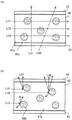
A display device according to a first embodiment will be described with reference to fig. 1. Fig. 1 is a diagram showing an example of the structure of the display device according to the first embodiment. Fig. 1(a) is a plan view of the display device of the first embodiment. FIG. 1B is a sectional view taken in the arrow direction A1-A2 in FIG. 1A. Fig. 1(a) and (B) are diagrams schematically showing a display device, and are not necessarily the same as actual sizes and shapes.
As shown in fig. 1(a), in the display device 1 of the first embodiment, the outer surface of the transparent substrate 2 is opened, and the plane of the transparent substrate 2 is visible from the viewer's point of view. The light source 8 is disposed along one side of the plane of the transparent substrate 2. Further, a plane of the light modulation layer 4 is formed below the plane of the transparent substrate 2. The planar region formed by the light modulation layer 4 serves as a display region.
The structure of the display device 1 will be described. As shown in fig. 1 (B), the transparent substrate 2 includes a pair of transparent substrates 2a and 2B arranged at a distance from each other, and a light modulation layer 4 is provided between the transparent substrates 2a and 2B. The outer surfaces of the transparent substrates 2a and 2b opposite to the light modulation layer 4 side are opened. In addition, the light source 8 is configured to emit light toward the light modulation layer 4 from the side surface of the light modulation layer 4.
Here, the light modulation layer 4 includes a first light modulation element 4a and a second light modulation element 4b having predetermined refractive index anisotropy. The first light modulation element 4a and the second light modulation element 4b have different responsivities to an electric field generated by electrodes provided on the transparent substrates 2a and 2 b. For example, the responsiveness of the second light modulator 4b to an electric field is relatively improved compared to the responsiveness of the first light modulator 4a to an electric field.
In such a light modulation layer 4, when no electric field is generated in the light modulation layer 4, there is almost no difference in refractive index between the first light modulation element 4a and the second light modulation element 4b in all directions including the front direction and the oblique direction. Therefore, the incident light from the light source 8 incident from the side surface of the light modulation layer 4 is directly transmitted and is not emitted to the transparent substrates 2a and 2 b. Light that has passed through the transparent substrate 2a, the light modulation layer 4, and the layer stacked on the transparent substrate 2b in the direction of passage also passes through. Thus, the light modulation layer 4 has high transparency when no electric field is generated, and when the plane of the transparent substrate 2a is defined as the front surface, the observer can visually recognize light incident from the outside to the transparent substrate 2b defined as the rear surface. In the following description, a state in which the light modulation layer 4 transmits incident light is referred to as a "transparent state". Note that the front direction is a direction in which the plane of the transparent substrate 2 is visually recognized, and the oblique direction is a direction other than the direction.
On the other hand, when an electric field is generated in the light modulation layer 4, a refractive index difference corresponding to the difference in responsivity between the first light modulation element 4a and the second light modulation element 4b increases in all directions. Therefore, the incident light from the light source 8 is scattered in the light modulation layer 4, and the scattered light is emitted toward the transparent substrates 2a and 2 b. Therefore, the observer can visually confirm the scattered light emitted from the transparent substrate 2 a. In the following description, a state in which the light modulation layer 4 scatters incident light is referred to as a "scattering state".
According to the display device 1 described above, by controlling the voltage applied to the electrode that generates an electric field in the light modulation layer 4 to switch the generation and extinction of the electric field generated in the light modulation layer 4, the light modulation layer 4 can be switched between the transparent state and the scattering state.
In the display device 1, in a state where no electric field is generated in the light modulation layer 4, there is almost no difference in refractive index between the first light modulation element 4a and the second light modulation element 4b in all directions, and therefore high transparency can be obtained regardless of the direction from which they are viewed. In general, in general PDLC, transparency is low because the PDLC is transparent in the front direction but has scattering properties in the oblique direction in principle. In contrast, the display device 1 has high transparency in all directions. Although the transparent substrate 2a side is described as a surface, the same applies to the transparent substrate 2b as a surface.
As shown by the chain line in fig. 1, the display device 1 may be configured to divide a display region and switch between a transparent state and a scattering state for each of the divided regions. In this way, an image can be displayed by controlling the transparent state and the scattering state for each divided region. In the example of fig. 1, the display region is divided into a matrix, but the present invention is not limited to this. For example, the display region may be switched by one electrode, or the display region may be switched by arranging electrodes only in a part of the display region and switching between generation and extinction of an electric field only in a part of the display region.
Further, although the display device 1 has been described as an embodiment of the present invention, the present invention is not limited thereto. For example, the illumination device may use light emitted from the display device 1 as illumination. In addition, the display device 1 does not always have to perform display. For example, the transparent substrate 2 may be used as a transparent plate such as a window glass in a normal state to display an image as needed. According to the display device 1, high transparency is provided in a state where no voltage is applied to the electrodes, and such use is also possible.
The display device described below as an embodiment is not limited to a narrow display device, and can be applied to various forms.
[ second embodiment ]
Next, a display device according to a second embodiment will be described. First, the structure of the display device will be described.
(1) Structure of the product
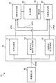
Fig. 2 is a diagram showing an example of the structure of the display device according to the second embodiment.
The display device 10 shown in fig. 2 has: a display panel 20, a panel driving circuit 30, a side light source 40, a light source driving circuit 50, an image output section 60, and a synchronization driving section 70. The display device 10 is an embodiment of the display device 1 shown in fig. 1. Hereinafter, for convenience, the horizontal direction, the vertical direction, and the depth direction in the case where the display panel 20 is visually recognized from the front direction are referred to as the X direction, the Y direction, and the Z direction, respectively, and are applied to the description as needed.
As shown in fig. 1, the display panel 20 includes a pair of transparent substrates 2 spaced apart from each other with a light modulation layer 4 interposed therebetween. The outer surface opposite to the light modulation layer 4 side is opened, and an observer can visually recognize the light emitted from the light modulation layer 4 through the outer surfaces of the pair of transparent substrates 2. In the following description, a region where the light modulation layer 4 emits light and the color can be visually recognized by an observer is referred to as a display region. The display panel 20 performs display control for each display unit, with the divided area obtained by dividing the display area as a display unit. In the following description, the display unit is referred to as a display cell Cpq. In the example of fig. 2, the display cells Cpq are arranged in a two-dimensional matrix. Let p denote the position in the row direction and q denote the position in the column direction.
The panel driving circuit 30 controls the application of a voltage to the electrodes that cause the generation and extinction of the electric field to occur on each light modulation layer region corresponding to the display cell Cpq. In the panel driving circuit 30, voltages are applied to the electrodes in units of display cells Cpq in accordance with a driving signal input from the synchronous driving section 70, and the electrodes are sequentially driven, thereby switching between the scattering state and the transparent state of the light modulation layer region of each display cell Cpq.
The side light source 40 is disposed along the side of the display panel 20, and inputs light of a predetermined color to the light modulation layer 4 of the display panel 20. The side light source 40 has a plurality of color light sources that emit lights of different colors and are independently controlled. For example, there are a first color light source emitting a first primary color light, a second color light source emitting a second primary color light, and a third color light source emitting a third primary color light. In the second embodiment, the first primary color is red, the second primary color is green, and the third primary color is blue. In addition, instead of the first primary color, the second primary color, and the third primary color, a light source of any color in a complementary color relationship may be combined and used. Further, the display device may display a single color.
The light source driving circuit 50 drives each light source of the side light sources 40 in accordance with a driving signal from the synchronous driving section 70.
The image output section 60 outputs the image signal SRGB to the synchronous drive section 70. Color information corresponding to the display area of the display panel 20 is set in the image signal SRGB. The image signal SRGB includes, for example, a signal value Rpq of a red component, a signal value Gpq of a green component, and a signal value Bpq of a blue component corresponding to the display cell Cpq. In the following description, it is assumed that in the image signal SRGB, the color information of the display cell Cpq is set for each display cell Cpq by the red component Rpq, the green component Gpq, and the blue component Bpq. Further, the image signal SRGB may not correspond to one to the display unit Cpq.
The synchronous driving section 70 acquires the image signal SRGB, synchronously drives the panel driving circuit 30 and the light source driving circuit 50. Specifically, the electrode driving by the panel driving circuit 30 and the light incidence from the side light source 40 driven by the light source driving circuit 50 are synchronized with respect to the display cell Cpq.
The details of each component will be described in turn.
First, the display panel 20 will be explained. Fig. 3 is a diagram showing the structure of the display panel of the second embodiment. Fig. 3 (a) is a cross-sectional view of the display panel. Fig. 3 (B) is a diagram showing an example of the state of the light modulation layer when no voltage is applied. Fig. 3 (C) is a diagram showing an example of the state of the light modulation layer at the time of voltage application. In fig. 3 (B) and (C), refractive index anisotropies of the light modulation elements included in the light modulation layer are represented by refractive index ellipsoids. The refractive index ellipsoid is a tensor ellipsoid that shows the refractive index of linearly polarized light incident from various directions, and by observing an ellipsoid cross section taken in the direction of light incidence, the refractive index can be geometrically known.
As shown in fig. 3 (a), the display panel 20 includes: a lower transparent substrate 22 and an upper transparent substrate 23 arranged to be spaced apart from each other, a lower electrode 31 provided on a surface of the lower transparent substrate 22 facing the upper transparent substrate 23, an upper electrode 32 provided on a surface of the upper transparent substrate 23 facing the lower transparent substrate 22, and a light modulation layer 80 arranged between the lower transparent substrate 22 and the upper transparent substrate 23. The side light source 40 is disposed at a position facing the light modulation layer 80 on the side surface of the display panel 20. The outer surfaces of the lower transparent substrate 22 and the upper transparent substrate 23 opposite to the light modulation layer 80 are opened so as to be visually recognized by an observer.
The lower transparent substrate 22 and the upper transparent substrate 23 support the light modulation layer 80, and are generally composed of a substrate transparent to visible light. Examples of the material of such a substrate include a glass plate and a resin substrate.
The lower electrode 31 and the upper electrode 32 generate an electric field between the lower electrode 31 and the upper electrode 32 by applying a voltage, and the electric field is applied to the light modulation layer 80 therebetween. The lower electrode 31 and the upper electrode 32 are both formed of a transparent material. The shapes of the lower electrode 31 and the upper electrode 32 are different depending on the driving method, but in any driving method, it is possible to generate an electric field independently for each region corresponding to the display cell Cpq, with the display cell Cpq as a driving unit. The structures of the lower electrode 31 and the upper electrode 32 will be described later.
The light modulation layer 80 is a layer including two kinds of light modulation elements. The refractive index anisotropy of the two light modulation elements is the same, and the responsiveness to an electric field is different. In the display panel 20 shown in fig. 3, a composite layer is formed including a liquid crystalline monomer 81 and liquid crystal molecules 82 dispersed in the liquid crystalline monomer 81. Here, the ordinary refractive index and the extraordinary refractive index of the liquid crystal monomer 81 and the liquid crystal molecule 82 are equal to each other. Further, a deviation in refractive index caused by, for example, a manufacturing error or the like is allowed. On the other hand, the liquid crystal molecules 82 have higher responsiveness to an electric field than the liquid crystal monomers 81. The liquid crystal monomer 81 has, for example, a stripe structure or a porous structure that does not respond to an electric field, or a rod structure having a response speed slower than that of the liquid crystal molecules 82. The liquid crystal monomer 81 is an embodiment of the first light modulator 4a, and the liquid crystal molecule 82 is an embodiment of the second light modulator 4 b. The liquid crystalline monomer 81 is preferably a monomer that can be polymerized by light or heat curing. When the liquid crystal monomer is polymerized and converted to a polymer, the liquid crystal molecules 82 and the liquid crystal polymer (polymer material) are preferably cured so that the ordinary refractive index and the extraordinary refractive index are always equal to each other. Further, the liquid crystal molecules 82 preferably have higher responsiveness to an electric field than the liquid crystal polymer. Hereinafter, the liquid crystalline polymer will be described in accordance with a liquid crystalline polymer obtained by polymerizing the liquid crystalline monomer. The light modulation layer 80 of the present embodiment can be applied to a Polymer Dispersed Liquid Crystal (PDLC) which is a composite layer in which Liquid Crystal molecules 82 are Dispersed in the Polymer material.
For example, as shown in fig. 3B, in a state where no voltage is applied between the lower electrode 31 and the upper electrode 32 and no electric field is generated in the light modulation layer 80, the directions of the optical axis AX1 of the liquid crystal cell 81a and the optical axis AX2 of the liquid crystal molecule 82a are aligned (parallel) with each other. Further, the optical axes AX1, AX2 refer to lines parallel to the traveling direction of such light rays that the refractive index is a value regardless of the polarization direction. In this case, the direction of the optical axis AX1 and the direction of the optical axis AX2 may be slightly shifted due to, for example, manufacturing errors.
On the other hand, as shown in fig. 3 (C), in a state where a voltage is applied between the lower electrode 31 and the upper electrode 32 and an electric field is generated in the light modulation layer 80, the direction of the optical axis AX1 of the liquid crystal cell 81b intersects the direction of the optical axis AX2 of the liquid crystal molecule 82 b.
The operation of this light modulation layer 80 will be explained. Fig. 4 is a schematic diagram illustrating the operation of the light modulation layer of the second embodiment. Fig. 4 (a) is a schematic diagram showing the action of the light modulation layer under no voltage application, and fig. 4 (B) is a schematic diagram showing the action of the light modulation layer under voltage application.
In the state where the voltage (a) in fig. 4 is not applied, no voltage is applied between the upper electrode 32 and the lower electrode 31, and no electric field is generated in the light modulation layer 80. In this state, as shown in fig. 3 (B), the directions of the optical axis AX1 of the liquid crystal cell 81a and the optical axis AX2 of the liquid crystal molecule 82a coincide with each other, and there is almost no refractive index difference in all directions including the front direction and the oblique direction. Therefore, for example, the incident lights L11, L12, and L13 of the side light source 40 shown by the dashed-dotted line and incident from the side surface are transmitted through the light modulation layer 80 without being scattered in the light modulation layer 80. The light from the side light source 40 toward the lower transparent substrate 22 or the upper transparent substrate 23 is totally reflected and does not exit to the outside. Light L21 and L22, which are indicated by dashed lines and are incident from the outside of the lower transparent substrate 22 in the penetrating direction penetrating through the lower transparent substrate 22, the light modulation layer 80, and the upper transparent substrate 23, are not scattered in the light modulation layer 80, pass through the light modulation layer 80, and are emitted from the upper transparent substrate 23. Thus, when no voltage is applied between the lower electrode 31 and the upper electrode 32, the light modulation layer 80 has high transparency.
On the other hand, in the voltage applied state in fig. 4 (B), a voltage is applied between the upper electrode 32 and the lower electrode 31, and an electric field is generated in the light modulation layer 80. In this state, as shown in fig. 3 (C), the direction of the optical axis AX1 of the liquid crystal monomer 81b intersects the direction of the optical axis AX2 of the liquid crystal molecule 82b, and the refractive index difference increases in all directions including the front direction and the oblique direction, and thus high scattering property is obtained. For example, the incident lights L11, L12, and L13 from the side light source 40 that enters from the side are scattered in the light modulation layer 80, and the scattered lights L31 and L32 are emitted from the upper transparent substrate 23. Accordingly, when the upper transparent substrate 23 is viewed from the upper direction in fig. 4 (B), the scattered lights L31 and L32 can be visually confirmed. The same applies to the case where the lower transparent substrate 22 is viewed from the lower direction in fig. 4 (B).
In the display device 10 having such a configuration, when the upper transparent substrate 23 or the lower transparent substrate 22 is viewed from the front, light transmitted in the penetrating direction can be visually confirmed in a state where no voltage is applied. On the other hand, in the voltage applied state, the incident light from the side light source 40 that is emitted by being scattered in the light modulation layer 80 can be visually confirmed.
Next, the panel driving circuit 30 will be explained. Fig. 5 is a diagram showing the structure of a panel drive circuit according to the second embodiment.
The panel driving circuit 30 controls generation and extinction of an electric field corresponding to the display cell Cpq by selectively driving the lower electrode 31 and the upper electrode 32 by connecting the plurality of lower electrodes 31 and the plurality of upper electrodes 32 in a band shape.
The lower electrode 31 is a transparent electrode provided on the lower transparent substrate 22, and has a strip shape extending in one direction in the plane of the lower transparent substrate 22. The upper electrode 32 is a transparent electrode provided on the upper transparent substrate 23, and has a strip-like shape extending in one direction in the plane and in a direction intersecting with the extending direction of the lower electrode 31. The portion where the lower electrode 31 and the upper electrode 32 intersect is a region corresponding to the display cell Cpq. Further, the extending direction of the lower electrode 31 and the extending direction of the upper electrode 32 may be orthogonal to each other.
The panel drive circuit 30 performs a simple matrix drive control for sequentially driving the plurality of lower electrodes 31 and the plurality of upper electrodes 32. By adopting the simple matrix driving, it is not necessary to provide wiring or the like in the plane of the display panel 20, and higher transparency can be obtained.
In addition, one electrode may be formed of a solid film (that is, not formed after film formation), and the other electrode may be formed in a minute rectangular shape to perform active matrix driving of the electrodes. Various driving modes for driving the light modulation layer 80 for each display cell Cpq are known, and the panel driving circuit 30 can be configured by appropriately adopting such driving modes according to the application of the display device 10.
Next, the side light source 40 will be explained. Fig. 6 is a diagram showing the structure of a side light source of the second embodiment.
The side light source 40 has a structure in which light source units 41, 42, 43, 44, 45, and 46 are sequentially arranged along one direction of the display area of the display panel 20, and is connected to a light source driving circuit 50 that drives each light source.
The light source unit 41 includes a red light source 41R emitting red light, a green light source 41G emitting green light, and a blue light source 41B emitting blue light. The red light source 41R, the green light source 41G, and the blue light source 41B are connected to the light source drive circuit 50, respectively, and can be driven independently. The other light source units 42, 43, 44, 45, 46 also have the same configuration. In addition, unless the light source unit is specifically specified for explanation, the light sources of the respective colors constituting the light source unit are expressed as a red light source 4nR, a green light source 4nG, and a blue light source 4 nB.
The light source driving circuit 50 drives the red light source 4nR, the green light source 4nG, and the blue light source 4nB, respectively, in accordance with a driving signal from the synchronous driving section 70. For example, by lighting the red light source 41R of the light source unit 41, red light is incident on the region of the light modulation layer 80 corresponding to the display cell row arranged at the left end of the display panel 20. Light of the respective colors is incident on the green light source 41G and the blue light source 41B in the same manner. The light source driving circuit 50 can sequentially emit the incident light of each color into the light modulation layer 80 in synchronization with the panel driving circuit 30, and display a desired color in units of display cells Cpq. Further, the red light source 4nR, the green light source 4nG, and the blue light source 4nB may be lit at a single color, or may be lit at a plurality of colors at the same time. For example, if the red light source 4nR and the blue light source 4nB are simultaneously lit, light of magenta can be incident on the display panel 20. Similarly, all of the red light source 4nR, the green light source 4nG, and the blue light source 4nB may be turned on to emit white light. For example, in the case of performing monochrome display, the light-on time and the light emission intensity of each light source may be combined to form light of a desired color, and the light may be incident on the light modulation layer 80.
In the example of fig. 6, one light source unit is arranged for one display unit row, but a plurality of light source units may be arranged for one display unit row. The red light sources 4nR, the green light sources 4nG, and the blue light sources 4nB are arranged in the extending direction of the side light sources 40, but may be arranged in a direction perpendicular to the extending direction of the side light sources 40, for example. The arrangement of the light sources is not limited as long as light of three primary colors can be incident on the display cell columns, respectively.
Next, a hardware configuration will be described. Fig. 7 is a diagram showing a hardware configuration of the second embodiment.
The entire device of the display device 10 is controlled by the control section 90. The control Unit 90 includes a CPU (Central Processing Unit) 91, and a RAM (Random Access Memory) 92 and a ROM (Read Only Memory) 93 and a plurality of peripheral devices are connected to the CPU 91 via a bus 96.
The CPU 91 is a processor that realizes the processing function of the control section 90.
The RAM92 is used as a main storage device of the control section 90. The RAM92 temporarily stores at least a part of programs and application programs of an OS (Operating System) to be executed by the CPU 91. The RAM92 stores various data necessary for the processing of the CPU 91.
The ROM 93 is a read-only semiconductor storage device, and stores programs of an OS, application programs, and fixed data that is not rewritten. In addition, a semiconductor memory device such as a flash memory can be used as a secondary memory device in place of the ROM 93 or in addition to the ROM 93.
The peripheral devices connected to the bus 96 include the panel driving circuit 30, the light source driving circuit 50, the input interface 94, and the communication interface 95.
The display panel 20 is connected to the panel drive circuit 30.
The side light source 40 is connected to the light source drive circuit 50.
An input device for inputting a user's instruction and an interface for acquiring an image signal from another device are connected to the input interface 94. The input interface 94 transmits signals transmitted from an input device or other devices to the CPU 91.
The communication interface 95 is connected to a network 98. The communication interface 95 transmits and receives data to and from other computers or communication devices via a network 98.
The processing function of the present embodiment can be realized by the hardware configuration described above. The above-described structure is an example, and the structure can be changed as appropriate.
Further, the image output section 60 and the synchronous drive section 70 shown in fig. 2 realize their processing functions by the control section 90.
Next, a functional configuration of the display device 10 will be described. Fig. 8 is a block diagram showing a functional configuration of the display device of the second embodiment.
The display device 10 has a synchronous drive section 70, and the synchronous drive section 70 synchronously drives the panel drive circuit 30 and the light source drive circuit 50 in accordance with the image signal SRGB input from the image output section 60. The synchronization driving section 70 includes a timing generation section 71 that generates a synchronization signal STM, a display unit driving signal generation section 72, and a light source driving signal generation section 73.
The processing of each part of the synchronous drive unit 70 will be described.
The timing generation section 71 generates a synchronization signal STM that synchronizes the operation timings of the panel drive circuit 30 and the light source drive circuit 50. The generated synchronization signal STM is output to the panel driving circuit 30 and the light source driving circuit 50.
The display cell drive signal generating section 72 generates a display cell drive signal SCEL for driving the electrodes corresponding to the display cells Cpq based on the image signal SRGB, and outputs the display cell drive signal SCEL to the panel drive circuit 30 together with the synchronization signal STM. The display cell drive signal SCEL is set with drive values corresponding to the red component Rpq, the green component Gpq, and the blue component Bpq included in the image signal SRGB.
The light source drive signal generating section 73 generates a light source drive signal LRGB for driving the red light source 4nR, the green light source 4nG, and the blue light source 4nB corresponding to the display unit Cpq based on the image signal SRGB, and outputs the light source drive signal LRGB to the light source drive circuit 50.
The panel driving circuit 30 and the light source driving circuit 50 are synchronously driven according to the synchronization signal STM. For example, in synchronization with the light source driving circuit 50 lighting up the red light source 4nR in accordance with the light source driving signal LRGB, the panel driving circuit 30 applies a voltage of the red component Rpq of the target display cell Cpq corresponding to the display cell driving signal SCEL to the electrode of the target display cell Cpq. As a result, red scattered light corresponding to the luminance of the red light source 4nR incident through the light source driving circuit 50 and the voltage applied to the electrodes by the panel driving circuit 30 is emitted from the object display cell Cpq. The same applies to other colors.
By thus synchronously driving the panel driving circuit 30 and the light source driving circuit 50, the display of the red component Rpq, the green component Gpq, and the blue component Bpq of the image signal SRGB is reproduced on the display cell Cpq.
In the synchronous drive section 70, in order to reproduce each color component, the light emission time or light emission intensity (luminance) of the red light source 4nR, the green light source 4nG, and the blue light source 4nB and the time or voltage application to the electrode are appropriately determined in accordance with the image signal SRGB.
(2) Display function
Next, a functional process of the display device 10 having the above-described configuration will be described with reference to fig. 9.
Fig. 9 is a diagram for explaining an example of synchronous drive control according to the second embodiment. In fig. 9, the synchronous drive unit 70 is omitted.
The panel drive circuit 30 performs a simple matrix control of sequentially applying voltages to electrodes that cause electric fields to be generated in the light modulation layer 80 corresponding to the display cells Cpq. In one image display frame in which an image based on the image signal SRGB is displayed on the display panel 20, the panel drive circuit 30 controls the one display cell Cpq to apply a voltage to the electrodes three times in total when the side light source 40 turns on the red light source 4nR, the green light source 4nG, and the blue light source 4nB, respectively. Thus, for one display cell Cpq, light based on the red component Rpq, the green component Gpq, and the blue component Bpq of the image signal SRGB is sequentially emitted from the light modulation layer 80, and the observer can visually recognize the color corresponding to the image signal SRGB. In addition, in the case where all the color components of the image signal SRGB are 0, the electrodes corresponding to the display cells Cpq are not driven, and the observer visually confirms the transparent state of the display cells Cpq.
For example, as shown in fig. 9, it is assumed that the light source unit 45 of the side light source 40 lights up the green light source 45G by the light source drive circuit 50 to which the synchronization signal STM and the light source drive signal LRGB are input. Thereby, the light source incident light L14 of the green light source 45G is incident on the light modulation layer region corresponding to the display cell C25. When the light source incident light L14 is incident on the light modulation layer region of the display cell C25, the panel drive circuit 30 applies a voltage to the electrode corresponding to the display cell C25 in accordance with the synchronization signal STM. The magnitude of the applied voltage or the application time is determined by the display cell drive signal generating section 72 according to the light intensity of the light source incident light L14 and the green component G25 of the display cell C25. Since a voltage is applied to the corresponding electrode, the light modulation layer region corresponding to the display cell C25 is in a scattering state, and the scattered light L31 of the light source incident light L14 is emitted, so that the observer can visually recognize the color green. The same processing is performed for the other display cells Cpq. Further, the same processing is performed for all the display cells Cpq with respect to the red component Rpq and the blue component Bpq, and one image display frame period ends.
In this way, the voltage application to the electrodes in the panel driving circuit 30 and the side light source 40 driving by the light source driving circuit 50 are performed in synchronization for each color component by the synchronization driving section 70, and a color based on the image signal SRGB is displayed on the display unit Cpq.
In the above description, the colors included in the image signal SRGB are the red component Rpq, the green component Gpq, and the blue component Bpq, and the lighting of the corresponding red light source 4nR, green light source 4nG, and blue light source 4nB is synchronized with the driving of the electrodes, but the present invention is not limited to this. For example, the color components may be cyan, magenta, and yellow, and the green light source 4nG and the blue light source 4nB, the red light source 4nR and the blue light source 4nB, and the red light source 4nR and the green light source 4nG may be turned on in each driving period. The color of the color light source provided in the side light source 40, the combination of colors of lights that are lit when driven, and the like can be appropriately selected in accordance with the desired display.
Further, the configuration and the driving method for driving the voltage application to the electrodes by the panel driving circuit 30 in synchronization with the driving of the side light sources 40 by the light source driving circuit 50 can be determined as appropriate. Hereinafter, field sequential control and line sequential control will be described as examples thereof. In the following description, the process of sequentially applying voltages to the electrodes corresponding to the display cells Cpq in a predetermined order is referred to as scanning.
The field sequential control is control for controlling switching of the color of the side light source 40 in units of display areas (fields) and scanning of the display cells Cpq in synchronization with the switching. On the other hand, the line sequential control is control for controlling switching of lighting colors of the side light sources 40 in units of a row of the side light sources 40 or a block consisting of a plurality of rows and scanning the display cells Cpq in synchronization with the switching.
First, field sequential control will be explained. Fig. 10 is a diagram showing an operation sequence of the field sequential control according to the second embodiment. Rpq, Gpq, and Bpq in fig. 10 indicate that the corresponding display unit Cpq is displaying red (R), green (G), and blue (B). Similarly, R, G, B corresponding to the light source units indicates that the light source units are each lighting up the red light source 4nR, the green light source 4nG, and the blue light source 4 nB.
In the field sequential control, as shown in fig. 10, the same color light sources of the side light sources 40 are simultaneously lit, all the display cells Cpq in the display area are scanned, and the lighting colors of the side light sources 40 are simultaneously switched after the scanning is completed, and the procedure is repeated.
In the example of fig. 10, the panel driving circuit 30 scans the display cells Cpq for each row in the order of the driving lines of the display cells C11-C19, the driving lines of the display cells C21-C29, …, and the driving lines of the display cells C51-C59. The light incident direction of the side light sources 40 incident in the Y direction of the display panel 20 shown in fig. 9 is different from the scanning direction of the display cell Cpq as the X direction.
In the field sequential control, since the light color of the side light sources 40 is switched on a field-by-field basis, in the example of fig. 10, the light source units 41 to 49 all turn on the red light sources 41R to 49R during the period from the first display cell C11 to the last display cell C59 in the first scan. The panel driving circuit 30 sequentially drives the electrodes corresponding to the display cells Cpq in accordance with the display cell driving signal SCEL acquired from the display cell driving signal generating section 72. Thereby, each display cell Cpq displays the red component Rpq of the image signal SRGB.
In synchronization with the timing at which the scanning of the last display unit C59 for red ends, the light source driving circuit 50 switches the light source that is lit from the red light sources 41R to 49R to the green light sources 41G to 49G for the light source units 41 to 49. In the second scanning, the light source units 41 to 49 all turn on the green light sources 40G, and the panel driving circuit 30 sequentially drives the electrodes corresponding to the display cells Cpq in accordance with the display cell driving signal SCEL. Thereby, each display cell Cpq displays green component Gpq of image signal SRGB.
In synchronization with the timing at which the scanning of the last display unit C59 for green ends, the light source driving circuit 50 switches the lighting light sources of the light source units 41 to 49 from the green light sources 41G to 49G to the blue light sources 41B to 49B. In the third scanning, the light source units 41 to 49 turn on all the blue light sources 41B to 49B, and the display unit Cpq displays the blue component Bpq of the image signal SRGB by the scanning of the panel driving circuit 30.
In this way, the red component Rpq, the green component Gpq, and the blue component Bpq are sequentially displayed, and an image based on the image signal SRGB is displayed on the display panel 20. In fig. 10, the display unit Cpq is set to be scanned in the X direction, but may be set to be scanned in the Y direction. The order of the incident colors may be different from the above order.
Next, the sequence control will be explained. Fig. 11 is a diagram showing an operation sequence of the line sequence control according to the second embodiment. The symbols shown in fig. 11 are the same as those in fig. 10.
In the example shown in fig. 11, the light source driving circuit 50 drives the light sources of the respective colors in the order of the light source units 41, 42, 43, 44, 45, 46, 47, 48, 49. The panel driving circuit 30 scans a group of display cells Cpq corresponding to the light sources of the respective colors and arranged in the incident direction in which light from the light sources advances in the light modulation layer 80. Specifically, the panel driving circuit 30 scans the display cells Cpq for each row in this order of the driving lines corresponding to the display cells C11 to C51 of the light source unit 41, the driving lines corresponding to the display cells C12 to C52 of the light source unit 42, …, and the driving lines corresponding to the display cells C19 to C59 of the light source unit 49. In this way, in the control shown in fig. 11, the light incidence direction of the side light sources 40 incident in the Y direction of the display panel 20 shown in fig. 9 and the scanning direction (Y direction) of the display unit Cpq become the same.
In the example of fig. 11, in the first scanning, the light source driving circuit 50 lights up the red light source 41R for the light source unit 41. The panel driving circuit 30 scans the corresponding display cells C11-C51 in the first column to display red components R11-R51. Then, the light source driving circuit 50 turns on the red light source 42R of the adjacent light source unit 42, and the panel driving circuit 30 scans the corresponding display cells C12 to C52 of the second row to display the red components R12 to R52. Thereafter, the same process is repeated for each column, and the light source driving circuit 50 drives the red light sources 49R of the light source unit 49. The panel driving circuit 30 scans the corresponding display cells C19 to C59 in the ninth column to display red components R19 to R59.
In the second scanning, the lighting light source of the light source unit 41 is switched from the red light source 41R to the green light source 41G. The panel driving circuit 30 scans the corresponding display cells C11-C51 in the first column to display green components G11-G51. Thereafter, the same treatment was repeated for each column to display green components G19-G59.
In the third scanning, the light source driving circuit 50 switches the lighting light source of the light source unit 41 from the green light source 41G to the blue light source 41B. The panel driving circuit 30 scans the corresponding display cells C11-C51 in the first column to display blue components B11-B51. Thereafter, the same treatment was repeated for each column to show blue components B19-B59.
In this way, the red component Rpq, the green component Gpq, and the blue component Bpq are sequentially displayed, and an image based on the image signal SRGB is displayed on the display panel 20. In fig. 11, the side light sources 40 are controlled on a light source unit basis, but the processing may be performed on a block basis in which several light source units are collected.
In the example shown in fig. 11, for example, the light source unit 41 is kept in the on state of the red (R) light source during the period after the red (R) light source of the light source unit 41 is turned on and the scanning of the display units C11 to C51 is performed. Since the incident light from the light source unit 41 that requires the red (R) light source is the period during which the corresponding display cells C11-C51 are scanned, the light may be controlled to be turned on only during this period. The same applies to other display cells Cpq of other colors.
By performing control in this manner, the power consumption of the side light source 40 can be reduced.
In addition to field sequential control and Line sequential control, a Multi-Line drive method (Multi-Line Selection) for simultaneously selecting a plurality of scan electrodes, which is known as a simple matrix type liquid crystal panel, may be used.
As described above, in the display device 10, the scanning of the display cells Cpq by the panel driving circuit 30 and the switching of the respective colors of the side light sources 40 by the light source driving circuit 50 are performed in synchronization by the synchronization driving section 70. Thus, the incident light that has entered the light modulation layer 80 corresponding to the display cell Cpq from the side light source 40 is scattered depending on the magnitude of the voltage when the voltage is applied to the electrodes, and is transmitted when the voltage is not applied. That is, in the display device 10, the display cell Cpq to which no voltage is applied to the electrode is visually confirmed in the transparent state, and the display cell Cpq to which a voltage is applied to the electrode is visually confirmed in the scattering state. In particular, in the display device 10 of the second embodiment, in a state where no voltage is applied to the electrodes, there is almost no difference in refractive index between the liquid crystalline monomer 81 and the liquid crystal molecules 82 contained in the light modulation layer 80, and high transparency can be obtained.
Since such a display device 10 can obtain high transparency in a state where no voltage is applied to the electrodes, it can be applied to a field where conventional general PDLCs are difficult to use. For example, when the state in which the electrodes of all the display cells Cpq of the display panel 20 are disconnected is assumed to be normal, the display panel 20 can be used to be in a transparent state in normal times and to display an image based on the image signal SRGB when display is necessary. In a transparent state in a normal state, an object placed on the back surface can be visually recognized by an observer, and therefore, a mirror, a blackboard, or the like may be placed in advance. In a normal state, an observer can use the mirror or the blackboard while visually checking it, but can display information while overlapping the mirror or the blackboard as necessary.
(3) Modification example
Next, a modified example of the second embodiment will be explained.
In the line-sequential control shown in fig. 11, light of a plurality of colors is simultaneously incident into the light modulation layer 80. For example, when the Light source is an LED (Light Emitting Diode), Light having relatively high directivity is incident, but there is a possibility that color mixing of the incident Light occurs at a color boundary where colors are different between adjacent Light source units. For clear display, it is preferable to prevent color mixing of incident light.
Therefore, the synchronous driving section 70 controls the driving of the panel driving circuit 30 and the light source driving circuit 50 so as not to generate the color mixture of the incident light. Specifically, the synchronous drive unit 70 controls the driving so that the light of the color light source of the same color is incident on the column of the display cell Cpq adjacent to the column of the display cell Cpq to be driven or the light is not incident thereon.
For example, the display cells Cpq are divided into sub-blocks parallel to the light incident direction of the side light sources 40, and are driven in an interlaced manner. Further, within the sub-blocks, the color of the incident light is made the same. For example, the display cells Cpq shown in fig. 9 are alternately scanned every sub-block, and the light source cells corresponding to the display cells Cpq which are not sub-blocks of the object are turned off in advance. Thus, the incident light incident on the display cells Cpq of the sub-block to be driven does not mix colors.
In addition, when the color of the light source is switched between the light source units, a non-lighting period of the light source may be provided. For example, the unlit time is set while the scanning of the display cells C11-C51 is being performed before the lighting light source of the light source unit 42 shown in fig. 11 is switched from the red light source 42R to the green light source 42G. During the scanning of the display cells C11-C51, since the adjacent light source units 42 are not lit, the light incident to the display cells C11-C51 is not mixed in color. In the scanning period of the next row of display cells C12-C52, although the adjacent light source unit 41 side is being lit, the light source of the same color as that of the light source unit 42 is lit, and therefore color mixing does not occur. The light source unit 43 adjacent to the other one is turned off and has no influence on the scanning of the display units C12-C52.
In this way, color mixing of incident light can be prevented by the control of the synchronous drive section 70. For example, the light source may be configured to physically improve the straightness of light so that adjacent light is not mixed. This structure will be described with reference to fig. 12 and 13.
Fig. 12 is a diagram illustrating an example of a structure for improving the straightness of incident light in the second embodiment. Fig. 12 is a structure in which an incident light diffusion preventing portion that prevents diffusion of emitted light from the side light source 40 that enters the light modulation layer 80 is provided between the side light source 40 and the display panel 20 in order to improve the straightness of incident light. The high-aspect-ratio pattern 401 or the lens 402 is disposed as an example of the incident light diffusion preventing section.
The high aspect ratio pattern 401 is provided to increase the aspect ratio of the resist pattern, and to provide a light passage in a lattice shape or a honeycomb shape, for example. The high aspect ratio pattern 401a shown in fig. 12 is a perspective view showing an example of the high aspect ratio pattern 401 having a lattice shape. The diffusion of incident light is suppressed by passing it through the high aspect ratio pattern 401 disposed on the path of incident light between the side light source 40 and the display panel 20.
The lens 402 has a function of condensing incident light that has entered the lens 402 from the side light source 40, and the incident light condensed by the lens is emitted to the light modulation layer 80, thereby improving the straightness of the incident light.
Fig. 13 is a diagram showing another example of a structure for improving the straightness of incident light in the second embodiment. In the structure shown in fig. 12, an incident light diffusion preventing portion is provided between the side light source 40 and the display panel 20, whereas in fig. 13, an intra-layer light diffusion preventing portion that prevents the incident light from diffusing in the light modulation layer 80 is provided. In fig. 13, the light modulation layer 80 between the lower transparent substrate 22 and the upper transparent substrate 23 is omitted.
In order to improve the straightness of the light incident into the light modulation layer 80, the in-layer light diffusion preventing portions are provided on the lower transparent substrate 22 and the upper transparent substrate 23 along the direction in which the incident light travels. In the example of fig. 13, the light guide pattern 24 is provided on the light modulation layer 80 side of the lower transparent substrate 22 of the display panel 20. Further, the columnar pattern 25 is provided on the side of the upper transparent substrate 23 opposite to the light modulation layer 80. In addition, both the light guide pattern 24 and the columnar pattern 25 may be provided, or only one may be provided.
The light guide pattern 24 is disposed between the adjacent display cells Cpq, for example, between the strip electrodes corresponding to the adjacent display cells Cpq. The light that has diffused to the side of the light guide pattern 24 is reflected by the light guide pattern 24, returning to the center side. Thereby, the incident light having entered the light modulation layer 80 can linearly travel in the passage provided by the light guide pattern 24.
The cylindrical pattern 25 is used to form cylindrical lenses in a pattern on the upper transparent substrate 23, and has a function of condensing incident light on a straight line in the extending direction of the cylindrical pattern 25. This can suppress the diffusion of incident light entering the light modulation layer 80, and improve the linearity.
As the light source of the side light source 40, a laser beam having high linearity can be used.
By physically improving the straightness of incident light in this way, a clear image without color mixing can be obtained.
[ third embodiment ]
Next, as a third embodiment, a structure in which a plurality of display panels 20 of the second embodiment are stacked will be described.
The display device 10 has a structure in which the display panels 20 are one piece, but since the display panels 20 have high transparency as described above, even if a plurality of display panels 20 are stacked, the same display as that of the structure in which the display panels 20 are one piece can be visually confirmed by an observer.
Fig. 14 is a diagram showing a configuration example of the third embodiment in which a plurality of display panels are stacked. The same components as those of the display device 10 shown in fig. 2 are denoted by the same reference numerals, and description thereof is omitted.
The display device 100 includes: the image output section 60, the synchronous drive section 170, the three-layered display panels 20R, 20G, 20B, the panel drive circuits 30R, 30G, 30B corresponding to the display panels 20R, 20G, 20B, the side light sources 40R, 40G, 40B, and the light source drive circuits 50R, 50G, 50B corresponding to the side light sources 40R, 40G, 40B. In fig. 14, for the sake of explanation, the positions of the display panels 20R, 20G, and 20B are described as being shifted, but the display regions thereof overlap.
The display panels 20R, 20G, and 20B and the panel driving circuits 30R, 30G, and 30B are the same as the display panel 20 and the panel driving circuit 30 shown in fig. 2.
The side light sources 40R, 40G, and 40B are provided opposite to the light source units 41 to 49 of the side light source 40 shown in fig. 2, respectively, including the red light source 4nR, the green light source 4nG, and the blue light source 4nB, and emit monochromatic light to the target display panels 20R, 20G, and 20B. Side light sources 40R are composed of only red light sources, side light sources 40G are composed of only green light sources, and side light sources 40B are composed of only blue light sources. The light source driving circuits 50R, 50G, and 50B are the same as the light source driving circuit 50 shown in fig. 2.
With this structure, the display panel 20R displays the red component Rpq on the display cell Cpq of the display panel 20R in accordance with the incident light from the side light source 40R. The display panel 20G displays the green component Gpq on the display cell Cpq of the display panel 20G in accordance with the incident light from the side light source 40G. Then, the display panel 20B displays the blue component Bpq on the display cell Cpq of the display panel 20B in accordance with the incident light from the side light source 40B. By overlapping the display panels 20R, 20G, and 20B, the observer can visually confirm the display based on the image signal SRGB.
Further, as described above, in the transparent state where no voltage is applied to the electrode corresponding to the display cell Cpq, the display cell Cpq can emit light incident from the back surface. For example, if the display cells Cpq corresponding to the display panels 20G and 20B are in a transparent state, the viewer can visually recognize the light emitted from the display panel 20R.
Therefore, the synchronous drive section 170 controls the panel drive circuits 30R, 30G, and 30B and the light source drive circuits 50R, 50G, and 50B so that the scanning lines of the display panels 20R, 20G, and 20B are different from each other. The synchronization driving section 170 generates a synchronization signal STM, a display unit driving signal SCEL, and a light source driving signal LRGB from the image signal SRGB input from the image output section 60. The display unit drive signal SCEL and the light source drive signal LRGB are separated for each color component and output to the panel drive circuits 30R, 30B, and 30G and the light source drive circuits 50R, 50G, and 50B of the corresponding color. The panel driving circuits 30R, 30B, and 30G are determined in advance so that the lines to start scanning are different from each other, and the synchronous driving unit 170 adjusts the control signal according to the lines to start scanning.
For example, when the panel driving circuits 30R, 30G, and 30B select rows of the display panels 20R, 20G, and 20B and sequentially scan the display cells Cpq in the row direction (horizontal direction), the start rows are shifted. It is assumed that the panel driving circuit 30R starts scanning from the first line, the panel driving circuit 30G starts scanning from the second line, and the panel driving circuit 30B starts scanning from the third line, and the respective panel driving circuits 30R, 30G, and 30B perform scanning in synchronization. Since the scanned rows are shifted among the display panels 20R, 20G, and 20B, for example, light emitted from the lower display panel 20G passes through the upper display panel 20R to which no voltage is applied to the electrodes of the corresponding row, and is visually recognized by the observer. Similarly, the light emitted from the lower display panel 20B passes through the upper display panels 20G and 20R, and is visually recognized.
With this configuration, the number of colors of the light sources of the respective colors arranged in the side light sources 40 of each display panel 20 can be reduced, and thus the display cell Cpq can be made smaller than in the case where the display panel 20 is one. Further, since the panel driving circuits 30R, 30G, and 30B only need to scan the respective colors, detailed display can be performed as compared with a case where the display panel 20 is constituted by one display panel. Also, if the size of the display unit Cpq is the same as that of the case where the display panel 20 is one block, the image can be updated at a higher speed.
In the above configuration, three display panels 20 are stacked, but the present invention is not limited to this. For example, two display panels 20 may be stacked, one of which is for red display and the other of which is for blue and green display. In addition, four display panels 20 may be stacked, and for example, a display panel 20 for displaying white may be added in addition to the display panels for red, green, and blue. Of course, a plurality of side light sources 40 may be overlapped to emit display panels 20 of the same color.
[ fourth embodiment ]
Next, a fourth embodiment will be explained.
In the second embodiment, the light source is provided as a side light source, and the fourth embodiment has a structure in which the light source is provided as an external light source.
Fig. 15 is a diagram showing an example of the structure of the display device according to the fourth embodiment. The same components as those of the display device 10 shown in fig. 2 are denoted by the same reference numerals, and description thereof is omitted.
The display device 200 includes: a display panel 20, a panel driving circuit 30, an image output section 60, an external light source 240, an external light source driving section 250, and a synchronization driving section 270.
The display panel 20, the panel driving circuit 30, and the image output unit 60 have the same configurations as those shown in fig. 2.
The external light source 240 includes a red external light source 240R that emits red light, a green external light source 240G that emits green light, and a blue external light source 240B that emits blue light, and the external light source 240 is disposed outside the display panel 20 and emits light of each color toward the display panel 20. Similarly to the side light sources 40, the colors of the respective color light sources of the external light source 240 are arbitrary. The external light source 240 may be disposed anywhere as long as it can emit light to the display panel 20.
The external light source driving unit 250 obtains the synchronization signal STM and the light source driving signal LRGB from the synchronization driving unit 270, and drives the external light source 240.
The synchronization driving section 270 acquires the image signal SRGB from the image output section 60, and generates a synchronization signal STM, a display cell driving signal SCEL, and a light source driving signal LRGB which synchronize the scanning timing of the display cell Cpq by the panel driving circuit 30 with the driving timing of the external light source 240 by the external light source driving section 250. The synchronization signal STM, the display cell drive signal SCEL, and the light source drive signal LRGB generate the same signals as those shown in fig. 8.
In the display device 200 having such a configuration, for example, display by field sequential control will be described. The external light source driving section 250 switches the output light source of the external light source 240 each time the scanning of the display cells Cpq of the display panel 20 by the panel driving circuit 30 is completed once. At the timing when the external light source driving section 250 drives the red external light source 240R, the panel driving circuit 30 scans the display cells Cpq in accordance with the red component Rpq. The same applies to other colors. When a voltage is applied to the electrodes of the display cell Cpq, incident light from the external light source 240 is scattered in the light modulation layer region of the display cell Cpq, and is emitted from the display panel 20. When no voltage is applied to the electrodes of the display cell Cpq, incident light from the external light source 240 passes through the light modulation layer 80. Thereby, the viewer can recognize the transparent state of the display cell Cpq.
In this way, even if the light source is changed from the side light source 40 to the external light source 240, the synchronous drive unit 270 can display an image on the display panel 20 in the same manner as in the case of the side light source 40. That is, the synchronization driving section 270 performs display by controlling the external light source driving section 250 and the panel driving circuit 30 to synchronize the time when light is incident from the external light source 240 with the time when a voltage is applied to the corresponding electrode with respect to the object display cell Cpq.
Since the side light sources 40 and the external light source 240 can be handled in the same manner, the side light sources 40 and the external light source 240 can be disposed in a mixed manner in the display device 200. For example, a light source unit composed of a red light source 4nR and a green light source 4nG may be arranged as the side light source 40, and a blue external light source 240B may be arranged as the external light source 240. In this case, for example, in the field sequential control shown in fig. 10, the period in which the side light source 40 turns on the blue light source 4nB can be replaced with the lighting period of the blue external light source 240B.
In this way, by replacing one color of the side light sources 40 with the external light source 240, the arrangement interval of the side light sources 40 can be narrowed, and finer display can be performed. For example, in the case where three red light sources 41R, green light sources 41G, and blue light sources 41B are arranged in the arrangement direction of the display cells Cpq as shown in fig. 6, the width of the display cells Cpq in the direction of the side light sources 40 can be narrowed by changing the number of color light sources to two.
In the structure in which a plurality of display panels 20 are stacked as shown in fig. 14, the external light source 240 may irradiate incident light to one or a plurality of display panels 20.
Further, the color of light incident from the side light source 40 and the color of light incident as the external light source 240 can be arbitrarily combined.
[ fifth embodiment ]
Next, a fifth embodiment will be explained.
In the second embodiment, the incident light or the outgoing light is set as natural light, and the fifth embodiment has a structure using polarized light.
Fig. 16 is a diagram showing an example of the structure of the display device of the fifth embodiment. The same components as those of the display device 10 shown in fig. 2 are denoted by the same reference numerals, and description thereof is omitted.
The display device 300 includes: an image output section 60, a synchronization drive section 370, display panels 321, 322, panel drive circuits 331, 332, side light sources (G)341, side light sources (R, B)342, and light source drive circuits 351, 352. In fig. 16, the positions of the display panels 321 and 322 are described as being shifted for explanation, but the display regions of the panels overlap.
The display panel 321 has the same configuration as the display panel 20 shown in fig. 3, and a voltage corresponding to color information is applied to the electrodes corresponding to the display cells Cpq by the panel driving circuit 331, thereby generating an electric field in the corresponding light modulation layer region. Further, light from the side light source (G)341 is incident on the light modulation layer 80. In the example of fig. 16, the side light source (G)341 is constituted by only a green light source emitting green light. Unlike the display panel 20 shown in fig. 3, the display panel 321 is oriented in the orientation direction 381 shown in fig. 16 by an orientation process (e.g., a rubbing process or a photo-orientation process).
The display panel 322 has the same structure as the display panel 321, and the electrodes corresponding to the display cells Cpq are driven by the panel driving circuit 332 to generate an electric field in the corresponding light modulation layer region. Further, light from the side light source (R, B)342 is incident on the light modulation layer region. The side light source (R, B)342 has a red light source (R) of red and a blue light source (B) of blue. Similarly to the display panel 321, the display panel 322 is aligned in an alignment direction 382 shown in fig. 16 by alignment processing.
The synchronous driving section 370 acquires the image signal SRGB from the image output section 60, synchronously drives the panel driving circuit 331 and the light source driving circuit 351, and the panel driving circuit 332 and the light source driving circuit 352. Further, the synchronization driving unit 370 synchronizes the timing at which the light source driving circuit 351 enters the light of the corresponding color with the timing at which the panel driving circuit 331 applies the voltage to the corresponding electrode in the target display cell Cpq. The same applies to the panel driving circuit 332 and the light source driving circuit 352. On the other hand, the display panel 321 and the display panel 322 may have a timing of at least one image frame period. As in the case of stacking the display panels 20 as shown in fig. 14, the timings may not be exactly the same between the display panels. Details will be described later.
Next, the orientation of the display panels 321 and 322 will be described.
In the example shown in fig. 16, the orientation directions 381, 382 are oriented in the horizontal direction of the light modulation layer 80, and are assumed to be oriented by, for example, orientation processing. In this case, the liquid crystalline monomer 81 of the light modulation layer 80 is aligned in the longitudinal direction of the stripe structure along the alignment direction. When an electric field is applied in this state, the liquid crystal molecules 82 tend to fall down in the longitudinal direction of the stripe structure, and the tilt orientations of the liquid crystal molecules 82 are aligned in the alignment direction as a whole.
In the display panels 321 and 322 according to the fifth embodiment, when the panel driving circuits 331 and 332 apply voltages to the electrodes to generate an electric field in the light modulation layer region, the tilt orientations of the liquid crystal molecules 82 in the light modulation layer region are aligned. Thereby, polarized light having a uniform direction is emitted from the light modulation layer region. In the example of fig. 16, the orientation direction 381 of the stacked display panels 321 is the same as the orientation direction 382 of the display panel 322, and light polarized in the same direction as the orientation direction is emitted from either the display panel 321 or the display panel 322.
The light emitted from the display panel 322 on the rear surface side is incident on the display panel 321 on the upper layer. The light modulation layer 80 of the display panel 321 is also formed in the same orientation direction 381, and if incident light from the rear surface is polarized in the same direction as the orientation direction, the incident light can pass through the light modulation layer 80. The transmission is also effective when an electric field is generated in the light modulation layer 80.
By using polarized light in this way, even if the display device 300 overlaps the display panels 321 and 322, an observer positioned on the display panel 321 side can visually confirm light emitted from both the display panels 321 and 322.
In the above configuration, the display panels 321 and 322 are oriented horizontally, but the present invention is not limited to this. The typical alignment method includes both the horizontal direction and the vertical direction, but any alignment method may be used as long as the tilt orientation of the liquid crystal molecules can be aligned when a voltage is applied to the electrodes. If the alignment is horizontal, as shown in fig. 16, the display panel 321 and the display panel 322 are subjected to alignment processing so that the alignment directions become the same in the display panel 321 and the display panel 322. In addition, in the case of Vertical Alignment, for example, PVA (Patterned Vertical Alignment) in which the tilt direction is controlled by an Alignment film capable of forming a pretilt angle or a fringe electric field of a fine electrode, MVA (Multi-domain Vertical Alignment) in which a resin narrow band pattern is formed, and the like are known.
Hereinafter, a display function of the display device 300 will be described.
In the display device 300, incident light is incident from the side light source (R, B)342 to the light modulation layer 80 of the display panel 322 from the side. The incident light is natural light without polarized light. When an electric field is generated on the light modulation layer region of the display cell Cpq by applying a voltage to the electrode corresponding to the display cell Cpq on which incident light has been incident, the incident light is scattered. The scattered light is polarized in the stripe direction of the liquid crystal monomer 81 along the alignment direction, and is emitted from the display panel 322 as emitted light.
Fig. 17 is a diagram illustrating an example of emission amount of polarized light in the fifth embodiment.
Fig. 17 (a) is a graph showing the emission amount of polarized light emitted from the display panels 321 and 322 and polarized in the direction corresponding to the alignment direction, which is the stripe direction of the liquid crystal monomer 81. Fig. 17 (a) shows that the amount of light emitted in the polarization direction that matches the orientation direction is large in the emitted light.
Fig. 17 (B) is a graph showing emission amounts of polarized light emitted from the display panels 321 and 322 and polarized in a direction perpendicular to the stripe direction. Fig. 17 (B) shows that the amount of light emitted in the polarization direction perpendicular to the alignment direction is small.
Thus, the light emitted from the display panels 321 and 322 is polarized in the alignment direction. The light emitted from the display panel 322 on the back side is incident on the display panel 321 on the upper side. The operation of the upper display panel 321 will be described.
Fig. 18 is a diagram illustrating an example of a relationship between the transmittance based on the polarization direction of light entering from the rear surface and the driving voltage in the fifth embodiment. The S-polarized light represents the transmittance when the polarization direction of the incident light coincides with the stripe direction (alignment direction) of the liquid crystal monomer 81. The P-polarized light represents the transmittance when the polarization direction of the incident light is orthogonal to the stripe direction of the liquid crystal monomer 81. The driving voltage is a voltage applied to an electrode that causes an electric field to be formed in the light modulation layer 80.
As is apparent from fig. 18, in a state where the electric field is not generated in the light modulation layer 80 in the vicinity of 0 driving voltage, both the incident light (S-polarized light) having the polarization direction aligned with the orientation direction and the incident light (P-polarized light) having the polarization direction orthogonal to the orientation direction are transmitted through the light modulation layer 80 and emitted from the display panels 321 and 322. When the modulation layer 80 is in a scattering state by applying a driving voltage to the electrodes, incident light (P-polarized light) having a polarization direction orthogonal to the alignment direction is scattered by the light modulation layer 80 and hardly transmitted. On the other hand, incident light (S-polarized light) having a polarization direction matching the alignment direction is not scattered in the light modulation layer 80, and passes through the light modulation layer 80.
Next, display control in the display device 300 having such a configuration will be described. In the display device 100 according to the third embodiment shown in fig. 14, in the display panels 20R, 20G, and 20B stacked, in order to transmit the light emitted from the display panels 20B and 20G in the lower layer through the display panel 20R in the upper layer, it is necessary to shift the scanning lines of the display panels 20R, 20G, and 20B, but this is not necessary in the display device 300.
Fig. 19 is a diagram illustrating an example of display control of the display device according to the fifth embodiment. Fig. 19 omits the panel driving circuits 331, 332 and the light source driving circuits 351, 352.
In the display device 300, the panel drive circuit 331 and the side light sources (G)341, and the panel drive circuit 332 and the side light sources (R, B)342 are synchronously driven by the synchronous drive section 370. Here, a case will be described where the scanning lines of the upper display panel 321 and the lower display panel 322 are regarded as the same, and the display cells Cpq of the respective display panels 321 and 322 overlapped one on another are driven in synchronization.
First, a case will be described in which the display cell C27a of the display panel 321 and the display cell C27b of the display panel 322 overlapping with the display cell C27a are driven in synchronization with each other. According to the red component R27 of the image signal SRGB, red light is incident from the side light source (R, B)342 to the display cell C27b of the display panel 322 of the lower layer, while a voltage is applied to the electrode corresponding to the display cell C27 b. Thus, the light modulation layer region of the display cell C27b scatters the incident red light and emits the red light Lr 1. The red light Lr1 is polarized in the same polarization direction (X direction in fig. 19) as the orientation direction 382 of the display panel 322. The red light Lr1 is incident on the display cell C27a of the display panel 321 on the upper layer from the rear surface. In the example shown in fig. 19, no voltage is applied to the electrode corresponding to the display cell C27a, and the red light Lr1 that has been incident is transmitted through the display cell C27a as it is. In this way, the viewer visually recognizes the red light Lr1 emitted from the lower display cell C27 b.
Next, a case where the display cell C32a of the display panel 321 and the display cell C32b of the display panel 322 overlapping with the display cell C32a are driven in synchronization will be described. Blue light is incident from the side light source (R, B)342 to the display cell C32b of the underlying display panel 322 while a voltage is applied to the electrode corresponding to the display cell C32 b. The light modulation layer region of the display cell C32b scatters the incident blue light and emits blue light Lb 1. Blue light Lb1 is polarized in the same polarization direction (X direction in fig. 19) as orientation direction 382 of display panel 322. The blue light Lb1 enters the display cell C32a of the upper display panel 321 from the rear surface. As shown in fig. 18, since the light modulation layer 80 of the display device 300 transmits light polarized in the same direction as the orientation direction 381, the display cell C32a transmits blue light Lb 1. In the example shown in fig. 19, green light is incident on the display cell C32a from the side light source (G)341, and a voltage is applied to the electrode corresponding to the display cell C32 a. The display cell C32a scatters the incident green light and emits green light Lg 1. The green light Lg1 is also polarized in the same polarization direction (X direction in fig. 19) as the orientation direction 381. Thus, the display unit C32a emits the blue light Lb1 of the display panel 322 that has been transmitted and the green light Lg1 that has scattered the incident light from the side light source (G) 341. Thus, the blue light Lb1 and the green light Lg1 are visually confirmed by the observer.
In this way, in the display device 300, the upper display panel 321 can transmit light from the lower display panel 322 incident from the rear surface and having the polarization direction aligned with the orientation direction, and scatter and emit light incident from the side light source (G) 341. This allows the stacked display panels 321 and 322 to display an image of one image signal SRGB. Since the processing of each color can be shared by a plurality of display panels, the number of lines that can be driven can be increased. Further, a sense of depth can be given to the display.
Although fig. 19 shows a structure in which two display panels 321 and 322 are stacked, the number of stacked display panels may be any number as long as display panels having the same structure as the display panels 321 and 322 are arranged so that the respective alignment directions are aligned. As described with reference to fig. 3 and 4, the light modulation layer 80 included in the display device 300 has high transparency in a state where no electric field is generated. Further, as shown in fig. 18, since the liquid crystal display panel has high transmittance even for incident light from the back surface having the same polarization direction and the same orientation direction, high transparency and clear display can be realized even if a plurality of display panels are stacked.
In the display device 300, the side light sources 341 and 342 are used as light sources of light to be scattered in the display cell Cpq, but an external light source 240 as shown in fig. 15 may be used. Further, it is assumed here that the external light source 240 is unpolarized light. In the case of the external light source 240, light similar to the side light sources 341 and 342 is emitted from the display panels 321 and 322. That is, when a voltage is applied to the electrode corresponding to the corresponding display cell Cpq, the liquid crystal molecules 82 in the light modulation region of the display cell Cpq are aligned with the alignment direction and tilted. Accordingly, the scattered light obtained by scattering the incident light from the external light source 240 is also emitted as light polarized in the orientation direction.
Since the side light sources 341 and 342 and the external light source 240 can be driven in the same manner, the display device 300 can be configured such that the external light source 240 and the side light sources 341 and 342 are mixed.
In this way, by using polarized light, scattering and transmission can be simultaneously generated on the display cell Cpq of the display panel 321. That is, in a state where a voltage is applied to the electrode corresponding to the display cell Cpq, transmission and scattering of light incident from the front surface or the back surface of the light modulation layer 80 can be switched according to the polarization plane of the incident light. By performing display control using polarized light in addition to switching between the scattering state and the transmission state described with reference to fig. 2 to 15, it is possible to make the display change rich.
Hereinafter, an embodiment of a display panel having liquid crystal molecules aligned in the tilt azimuth direction when a voltage is applied by alignment will be described with reference to fig. 20, 21, 22, and 23. In addition, the same applies to the configuration shown below in which the lighting of the light source in the form of the side light source or the external light source and the application of the voltage to the electrodes corresponding to the display cells Cpq are driven in synchronization. Therefore, a description of the synchronous drive in the following configuration is omitted.
[ sixth embodiment ]
Next, a sixth embodiment will be explained.
In the fifth embodiment, a structure in which a plurality of display panels having the same orientation direction are stacked is shown, and in the sixth embodiment, a display panel is constituted by one piece. While the light from the side light sources 341 and 342 is natural light that is not polarized in the fifth embodiment, the light is incident polarized in the sixth embodiment.
Fig. 20 is a diagram showing an example of the structure of the display device according to the sixth embodiment. (A) The case where the projector projects is shown, and (B) the case where the projector does not project is shown.
The display device 400 includes: a display panel 420, a side light source 440, and a projector light source 441 as an external light source. The display panel 420 includes the light modulation layer 80, and has been processed so that the alignment direction 428 becomes the horizontal direction (X direction) in fig. 20. The side light source 440 emits light of a predetermined color from the side of the display panel 420.
The projector light source 441 externally inputs light to the light modulation layer 80 of the display panel 420. By combining with the light of the color incident from the side light source 440, an image of the image signal SRGB can be displayed. The projector light source 441 is capable of emitting light polarized along a selected polarization direction. In the example of fig. 20, it is assumed that projector light source incident light PL1 polarized in a direction orthogonal to the orientation direction 428 of the horizontal direction and projector light source incident light PL3 polarized in a direction parallel to the orientation direction 428 can be selected.
Fig. 20 (a) shows a case where projector light source incident light PL1 polarized in a direction orthogonal to the orientation direction 428 from among the projector light sources 441 has been incident on the display panel 420. The display cells Cpq of the display panel 420, on which the projector light source incident light PL1 is incident, have a voltage applied to the electrodes, and an electric field is generated. The light modulation layer region corresponding to the display cell Cpq transmits light having a polarization direction parallel to the alignment direction 428 when the light incident from the back surface is the light. On the other hand, light having a direction polarized in a direction orthogonal to the orientation direction is scattered. Since the polarization direction of projector light source incident light PL1 is orthogonal to the orientation direction, it is scattered on the light modulation layer area. The scattered light PL2 is emitted to the outside and can be visually recognized by an observer. That is, the light emitted from the projector light source 441 is projected to the display panel 420.
On the other hand, (B) of fig. 20 shows a case where projector light source incident light PL3 polarized in a direction parallel to the orientation direction 428 from among the projector light sources 441 has been incident on the display panel 420. The display cell Cpq of the display panel 420 on which the projector light source incident light PL3 is incident has an electric field generated by applying a voltage to the electrode, as in the case of (a) of fig. 20. In the light modulation layer region corresponding to the display cell Cpq, the orientation direction 428 is parallel to the polarization direction of the incident projector light source incident light PL3, and therefore, this transmitted light PL4 is transmitted through the light modulation layer region. That is, the light emitted from the projector light source 441 is not projected to the display panel 420.
In this way, the display device 400 is formed such that the light modulation layer 80 of the display panel 420 is aligned in a predetermined alignment direction and the tilt azimuths of the liquid crystal molecules 82 are aligned when a voltage is applied to the electrodes. Therefore, in a state where a voltage is applied to the electrodes of the target display cell Cpq, the transmission state and the display state can be switched by controlling the polarization direction of the projector light source 441 incident on the display cell Cpq. In the example of fig. 20, when the incident light from the projector light source 441 is orthogonal to the orientation direction, the incident light is scattered to become scattered light PL 2. If the incident light from the projector light source 441 is parallel to the orientation direction, the incident light is transmitted through the light modulation layer region of the display cell Cpq.
[ seventh embodiment ]
Next, a seventh embodiment will be explained.
In the sixth embodiment, a configuration in which one display panel is used and a projector light source is used is shown, and in the seventh embodiment, a case in which a projector light source is used as a light source in a configuration in which two display panels are used is described. Fig. 21 is a diagram showing an example of the structure of the display device according to the seventh embodiment. Note that the same point as in the fifth embodiment is that the surface of the display panel 521 overlaps the surface of the display panel 522.
The display device 500 includes: display panel 521, side light source (R)541, display panel 522, side light source (B)542, and projector light source 543.
The display panel 521 has the light modulation layer 80, and the orientation direction 528 becomes the horizontal direction (X direction) in fig. 21. The side light source (R)541 is disposed at a side of the display panel 521.
The display panel 522 has the light modulation layer 80, and the orientation direction 529 becomes a vertical direction (Y direction) orthogonal to the orientation direction 528 of the display panel 521. The side light sources (B)542 are disposed on the side of the display panel 522 in a direction perpendicular to the side light sources (R) 541.
In addition, the side light sources are preferably identical in the longitudinal direction and the orientation direction in terms of polarized light emission and light extraction efficiency. Therefore, the side light sources (B)542 and (R)541 are located at different positions.
The projector light source 543 emits blue light Lb2 and green light Lg2 toward the display panel 521. In the example of fig. 21, blue light Lb2 emitted from projector light source 543 is polarized in the horizontal direction (X direction) of fig. 21, and the polarization direction is parallel to orientation direction 528 of display panel 521 and orthogonal to orientation direction 529 of display panel 522. The green light Lg2 is light polarized in the vertical direction (Y direction), and the polarized light direction is orthogonal to the orientation direction 528 of the display panel 521 and parallel to the orientation direction 529 of the display panel 522.
In the display panel 521 of the display device 500, when a voltage is applied to the electrode of the corresponding display cell C39a, light incident on the display panel 521 from the side light source (R)541 is scattered there, and red light Lr2 is emitted. Red light Lr2 is polarized in the same direction as orientation direction 528. Since the polarization direction of the green light Lg2 emitted from the projector light source 543 to the display panel 521 is orthogonal to the orientation direction 528, when a voltage is applied to the electrode of the corresponding display cell C26a, the green light Lg2 is scattered. On the other hand, since the polarization direction of the blue light Lb2 is the same as the orientation direction 528, even when a voltage is applied to the electrode of the corresponding display cell C23a, the blue light Lb2 passes through the display cell C23a and is emitted to the display panel 522.
The blue light Lb2 transmitted through the display panel 521 and incident on the display panel 522 is scattered on the display panel 522 because the polarization direction is orthogonal to the orientation direction 529 of the display panel 522.
Depending on the polarization direction of light emitted from the projector light source 543, the light can be displayed on the display unit 521 on the upper layer as in the case of the display unit C26a or can be displayed on the display panel 522 on the lower layer by being transmitted through the display unit 521 on the upper layer as in the case of the display units C23a and C23 b.
Further, if the polarization direction of the light emitted from the projector light source 543 is switched so that the blue light Lb2 is orthogonal to the orientation direction of the upper display panel 521 and the green light Lg2 is parallel to the orientation direction of the upper display panel 521, the display is reversed. In this way, by making the orientation direction 528 of the upper display panel 521 orthogonal to the orientation direction 529 of the lower display panel 522 and switching the polarization direction of light emitted from the projector light source 543, different images can be displayed on the display panels 521 and 522. The polarization direction of the light emitted from the projector light source 543 can be realized by disposing an element for rotating the polarization direction between the projector light source 543 and the display panel 521. The projector light source 543 may be made to have such a function.
In the configuration of fig. 21, the orientation direction of the upper display panel 521 is orthogonal to the orientation direction of the lower display panel 522, but a layer for changing the polarization plane may be disposed between the upper and lower layers with the same orientation direction.
Fig. 22 is a diagram showing a first modification of the display device of the seventh embodiment. The same parts as those in fig. 21 are denoted by the same reference numerals, and description thereof is omitted.
The display device 501 has a structure in which a display panel 521 and a display panel 523 are stacked with a λ/2 phase difference plate 560 interposed therebetween. The surface of the display panel 521 overlaps the surface of the display panel 523.
The display panel 521, the side light source (R)541, and the projector light source 543 are similar to fig. 21.
The λ/2 phase difference plate 560 is disposed between the display panel 521 and the display panel 523, and changes the polarization plane of the transmitted light.
In the display device 501 having such a configuration, a case will be described where the blue light Lb3 and the green light Lg3 having the same polarization direction as the orientation direction 528 of the display panel 521 are emitted from the projector light source 543 to the display panel 521.
Since the polarization directions of the blue light Lb3 and the green light Lg3 are the same as the orientation direction 528 of the display panel 521, the blue light Lb3 and the green light Lg3 are transmitted through the display panel 521 and enter the λ/2 phase difference plate 560. When the blue light Lb3 and the green light Lg3 are in a state where no voltage is applied to the electrodes of the corresponding display cells C24a and C26a, it is needless to say that the display cells C24a and C26a can transmit even in a state where a voltage is applied. The polarization planes of the blue light Lb3 and the green light Lg3 that have passed through the λ/2 phase difference plate 560 change to become polarization planes in a direction perpendicular to the orientation direction 530 of the display panel 523. On the display panel 523, when a voltage is applied to the electrodes of the corresponding display cells C24b and C26b, the color light Lb3 and the green light Lg3 are scattered.
Fig. 23 is a diagram showing a case where projector light having different polarization directions is incident on the structure of fig. 22.
The blue light Lb4 is similar to the case of the blue light Lb3 shown in fig. 22. Blue light Lb4 emitted from projector light source 543 transmits through display panel 521, is switched in polarization plane by λ/2 phase difference plate 560, and is then scattered by display cell C24b of display panel 523.
On the other hand, the green light Lg4 is different from that in fig. 22, and the polarization direction is orthogonal to the orientation direction 528 of the display panel 521. Therefore, the green light Lg4 is scattered on the display cell C26a of the display panel 521.
Accordingly, in the display device 521, the green light Lg4 of the projector light source 543 and the red light Lr4 of the side light source (R)541 are scattered in the corresponding display cell Cpq and visually recognized by the observer. In the display device 523, the blue light Lb4 of the projector light source 543 and the blue light of the side light source (B)544 are scattered by the corresponding display cell Cpq and visually recognized by the observer.
In this way, by providing a layer for switching the polarization plane of incident light between the display panel 521 and the display panel 523, display can be switched between the display panel 521 and the display panel 523.
The above-described structure is an example, and the present invention is not limited thereto. The number of display panels to be stacked and the orientation direction thereof, the arrangement of layers for switching the polarization plane between the display panels to which incident light is incident, the polarization direction of the projector light source, and the like can be combined to perform desired display.
Further, the processing functions described above can be realized by a computer. In that case, a program describing the processing contents of the functions to be provided by the display device is provided. The above-described processing functions are realized on a computer by executing that program in the computer. The program describing the processing content can be recorded in advance on a recording medium readable by a computer. Examples of the recording medium that can be read by a computer include a magnetic storage device, an optical disk, an magneto-optical recording medium, and a semiconductor memory. The magnetic storage device includes a Hard Disk Drive (HDD), a Flexible Disk (FD), a magnetic tape, and the like. The optical disk includes a DVD (Digital Versatile disk), DVD-RAM, CD (Compact disk) -ROM, CD-R (Recordable)/RW (ReWritable), and the like. The Magneto-Optical recording medium has MO (Magneto-Optical disk) and the like.
When the program is distributed, a portable recording medium such as a DVD or a CD-ROM on which the program is recorded is sold. Further, the program may be stored in advance in a storage device of the server computer, and the program may be transferred from the server computer to another computer via a network.
The computer executing the program stores, for example, the program recorded in the portable recording medium or the program transferred from the server computer in its own storage device. Then, the computer reads the program from its own storage device and executes processing according to the program. Further, the computer may read the program directly from the portable recording medium and execute the processing according to the program. The computer may be configured to successively execute processing according to the received program each time the program is transferred from a server computer connected via a network.
At least a part of the processing functions may be implemented in an electronic Circuit such as a DSP (Digital Signal Processor), an ASIC (Application Specific Integrated Circuit), or a PLD (Programmable Logic Device).
Various modifications and alterations can be made by those skilled in the art within the scope of the idea of the present invention, and those modifications and alterations are also within the scope of the present invention. For example, those skilled in the art can add, delete, or modify the design of the components, or add, omit, or modify the conditions of the processes, as appropriate, to the above-described embodiments, as long as the gist of the present invention is achieved.
(1) One aspect of the disclosed invention relates to a display device having: a pair of transparent substrates arranged to be spaced apart and opposed to each other; a light modulation layer including a plurality of light modulation elements that are arranged between the pair of transparent substrates, have predetermined refractive index anisotropy, and have different responsivities to an electric field generated by electrodes provided on the transparent substrates; and a light source that emits light of a predetermined color from a side surface of the light modulation layer, wherein the light modulation layer transmits incident light emitted from the light source when the electric field is not generated, and scatters the incident light when the electric field is generated and emits the light to the transparent substrate.
According to the display device described in (1), in the aspect of the invention disclosed in (2), the pair of transparent substrates have an outer surface side opposite to the light modulation layer side opened, and the light modulation layer has a transmittance that transmits light in a penetrating direction penetrating through the transparent substrates and the light modulation layer when the electric field is not generated in the light modulation layer, so that light incident from one outer surface side of the pair of transparent substrates is transmitted in the penetrating direction and emitted to the other outer surface side of the pair of transparent substrates.
The display device according to the invention as set forth in the item (1) or (2), in the aspect of the invention as set forth in the item (3), the electrode generates the electric field in the display unit in a divided region into which the display region is divided, the light source has a plurality of color light sources each independently operating to enter light of a different color into the display unit, and the display device includes a driving unit that acquires color information of the display region, and synchronously drives lighting of the color light sources corresponding to the color information and voltage application to the electrode for each of the display units based on the color information.
The display device according to (3) of the invention according to (4) is characterized in that the light source includes a first color light source for emitting a first primary color light, a second color light source for emitting a second primary color light, and a third color light source for emitting a third primary color light, and the driving section lights up the first color light source and applies a voltage corresponding to a color component of the first primary color included in the color information to the electrode, lights up the second color light source and applies a voltage corresponding to a color component of the second primary color included in the color information to the electrode, and lights up the third color light source and applies a voltage corresponding to a color component of the third primary color included in the color information to the electrode during one image display frame.
In the display device according to the aspect of the invention as described in the above (3) or (4), in the aspect of the invention as described in the above (5), the driving unit turns on the color light source corresponding to the color component for each color component included in the color information, and causes the light of the color component to be incident on the planar region of the light modulation layer, and sequentially applies the voltage to the electrodes of the display unit
The display device according to (3) or (4), in an aspect of the invention disclosed in (6), the driving unit turns on the color light source corresponding to a color component included in the color information and enters the light of the color component into an area of the display unit group of the light modulation layer for each display unit group including the display units arranged in an incident direction in which the light of the color light source enters, and sequentially applies the voltage to the electrodes of the display units included in the display unit group.
According to the display device described in (6), in the aspect of the invention disclosed in (7), the driving section causes the light source corresponding to the second display unit group adjacent to the first display unit group as a driving object to be lit up or lit off in the same color as the first display unit group.
The display device according to any one of (3) to (7), in an aspect of the invention disclosed in (8),
the electrode has: a plurality of first electrodes each having a strip shape extending in one direction in a plane of one of the pair of transparent substrates; and a plurality of second electrodes each having a strip shape extending in a direction intersecting with a direction in which the first electrode extends in a plane of the other of the pair of transparent substrates, wherein the display unit is formed in a portion where the first electrode intersects with the second electrode, and wherein the driving unit performs a simple matrix drive control for sequentially driving the first electrode and the second electrode.
The display device according to any one of (1) to (8), in an aspect of the invention disclosed in (9), an incident light diffusion preventing portion that prevents diffusion of light incident on the light source of the light modulation layer is provided between the light source and the light modulation layer.
The display device according to any one of (1) to (9), in an aspect of the invention disclosed in (10), the transparent substrate is provided with an in-layer light diffusion preventing portion that prevents light of the light source that advances in the light modulation layer from diffusing, and the in-layer light diffusion preventing portion is provided along a direction in which light incident on the light source in the light modulation layer advances.
The display device according to any one of (3) to (9), in an aspect of the invention disclosed in (11), wherein a first display panel and a second display panel each having the pair of transparent substrates, the light modulation layer, and the light source are stacked, and the driving unit shifts a position of a first scanning line for sequentially applying a voltage to the electrode in the first display panel and a position of a second scanning line for sequentially applying a voltage to the driven electrode in the second display panel, and synchronously drives the first display panel and the second display panel.
(12) One aspect of the disclosed invention relates to a display device having: a pair of transparent substrates arranged to be spaced apart and opposed to each other; a light modulation layer including a plurality of light modulation elements that are arranged between the pair of transparent substrates, have predetermined refractive index anisotropy, and have different responsivities to an electric field generated by electrodes provided on the transparent substrates; an external light source that inputs light of a predetermined color to the light modulation layer from outside the transparent substrate; and a driving part which acquires color information of a display region, synchronously drives lighting of the external light source and voltage application to the electrode according to the color information, and the light modulation layer transmits incident light from the light source when the electric field is not generated, and scatters the incident light and emits the incident light to the transparent substrate when the electric field is generated.
The display device according to (12) of the present invention is the one aspect of the invention disclosed in (13), wherein the display device includes a light source that inputs light of a predetermined color into the light modulation layer from a side surface of the light modulation layer, and the driving unit synchronously drives lighting of the external light source, lighting of the light source, and voltage application to the electrodes in accordance with the color information.
(14) One aspect of the disclosed invention relates to a display device in which a first display panel and a second display panel are arranged so as to overlap each other such that a tilt direction of the first display panel and the tilt direction of the second display panel are in the same direction, the first display panel and the second display panel each including: a pair of transparent substrates arranged to be spaced apart from each other and to face each other; and a light modulation layer including a first light modulation element and a second light modulation element which are arranged between the pair of transparent substrates and have predetermined refractive index anisotropy, the second light modulation element is formed so as to have a relatively higher responsiveness to an electric field generated by an electrode provided on the transparent substrate than the first light modulation element, and the tilt orientations of the second light modulation elements are made to coincide when responding to the electric field, the first display panel and the second display panel transmit incident light when the electric field is not generated, when the electric field is generated, the incident light component having the same oblique azimuth as the polarization direction is transmitted, the incident light component having the different oblique azimuth and polarization direction is scattered, and the polarized light polarized in the direction corresponding to the oblique azimuth is emitted to the transparent substrate.
In the display device according to the aspect of the invention as recited in the item (14), in the aspect of the invention as recited in the item (15), the first display panel has a light source that inputs light of a predetermined color into the light modulation layer from a side surface of the light modulation layer, and is disposed on a rear surface of the second display panel.
The display device according to (14) or (15), in an aspect of the invention disclosed in (16), a phase difference plate that changes a polarization plane of the incident light is provided between the first display panel and the second display panel.
The display device according to any one of (14) to (16), in an aspect of the invention disclosed in (17), the display device has an external light source that outputs polarized light polarized in a predetermined polarization direction, and the driving section synchronously drives lighting of the external light source, lighting of the light source, and voltage application to the electrodes according to the color information.
In the display device according to the aspect of the invention as described in the above (17), in the aspect of the invention as described in the above (18), an element for rotating a polarization direction of light emitted from the external light source is provided between the external light source and the modulation layer.
(19) One aspect of the disclosed invention relates to a display device having: a pair of transparent substrates arranged to be spaced apart and opposed to each other; and a light modulation layer including a first light modulation element and a second light modulation element which are arranged between the pair of transparent substrates and have predetermined refractive index anisotropy, the light modulation layer being formed such that the responsiveness of the second light modulation element to an electric field generated by an electrode provided on the transparent substrate is relatively higher than the responsiveness of the first light modulation element to the electric field, and the inclination orientation of the second light modulation element in response to the electric field is made to coincide, the light modulation layer transmitting the incident light when the electric field is not generated, transmitting the incident light component having the same inclination orientation and polarization direction when the electric field is generated, scattering the incident light component having the different inclination orientation and polarization direction, and emitting the polarized light polarized in the direction corresponding to the inclination orientation to the transparent substrate.
The display device according to any one of (1) to (19), in an aspect of the invention disclosed in (20), the light modulation layer is a layer in which liquid crystal molecules are dispersed in a polymer material.
Description of the symbols
1 display device 2, 2a, 2b transparent substrate
4 light modulation layer 4a first light modulation element
4b second light modulation element 8 light source
10 display device 20 display panel
22 lower transparent substrate 23 upper transparent substrate
24 light guide pattern 25 cylindrical pattern
30 lower electrode of panel driving circuit 31
32 upper electrode 40 side light source
41. 42, 43, 44, 45, 46, 47, 48, 49 light source unit
50 light source drive circuit 60 image output unit
70 synchronous drive part 71 timing generation part
72 display unit drive signal generating section 73 light source drive signal generating section
80 light modulation layer 81 liquid crystalline monomer
82 liquid crystal molecules 240 external light source
250 an external light source driving part.
Claims (19)
1. A display device is characterized by comprising:
a pair of transparent substrates;
an electrode provided on each of the pair of transparent substrates;
a liquid crystal layer disposed between the pair of transparent substrates and having a liquid crystalline polymer and liquid crystal molecules;
a light source that emits light of a predetermined color from a side surface of the liquid crystal layer toward the liquid crystal layer; and
a driving part driving the light source and the electrode,
the liquid crystal layer transmits incident light incident from the light source when an electric field is not generated between the electrodes, scatters the incident light and emits the incident light to the transparent substrate when the electric field is generated,
the electrode has a divided area dividing a display area as a display unit in which the electric field is generated,
the light source has a plurality of color light sources each independently operating and injecting light of different colors to the display unit,
the driving section acquires color information of the display region, synchronously drives lighting of the color light source corresponding to the color information and voltage application to the electrodes for each of the display units based on the color information, and
for each color component included in the color information, the color light source corresponding to the color component is turned on to make light of the color component incident on a planar region of the liquid crystal layer, and a voltage is sequentially applied to the electrodes of the display unit.
2. The display device according to claim 1,
the pair of transparent substrates are open on the outer surface side opposite to the liquid crystal layer side,
the liquid crystal layer has a light transmittance in a penetrating direction in which light penetrates the transparent substrates and the liquid crystal layer when the electric field is not generated in the liquid crystal layer, and transmits light incident from an outer surface side of one of the pair of transparent substrates in the penetrating direction and emits the light to an outer surface side of the other of the pair of transparent substrates.
3. The display device according to claim 1,
the driving section, for a display unit group including the display units arranged along an incident direction in which light of the color light source is incident,
the color light sources corresponding to the color components included in the color information are turned on to make light of the color components incident on the regions of the display unit groups of the liquid crystal layer, and voltages are sequentially applied to the electrodes of the display units included in the display unit groups.
4. The display device according to any one of claims 1 to 3,
the liquid crystalline polymer and the liquid crystal molecules have the same refractive index as each other, and have different responsivities to the electric field.
5. The display device according to claim 4,
the liquid crystal molecules have higher responsiveness to the electric field than the liquid crystalline polymer.
6. A display device is characterized by comprising:
a pair of transparent substrates;
an electrode provided on each of the pair of transparent substrates;
a liquid crystal layer disposed between the pair of transparent substrates and having a liquid crystalline polymer and liquid crystal molecules;
an external light source that irradiates light of a predetermined color to the liquid crystal layer from outside the transparent substrate; and
a driving part driving the external light source and the electrode,
the liquid crystal layer transmits incident light incident from the external light source when an electric field is not generated between the electrodes, scatters the incident light and emits the incident light to the transparent substrate when the electric field is generated,
the electrode has a divided area dividing a display area as a display unit in which the electric field is generated,
the external light source has a plurality of color light sources each independently operating and injecting light of different colors to the display unit,
the driving section acquires color information of the display region, synchronously drives lighting of the color light source corresponding to the color information and voltage application to the electrodes for each of the display units based on the color information, and
for each color component included in the color information, the color light source corresponding to the color component is turned on to make light of the color component incident on a planar region of the liquid crystal layer, and a voltage is sequentially applied to the electrodes of the display unit.
7. The display device according to claim 6,
a light source for emitting light of a predetermined color from a side surface of the liquid crystal layer toward the liquid crystal layer,
the driving section synchronously drives lighting of the external light source, lighting of the light source, and voltage application to the electrode based on the color information.
8. The display device according to claim 6 or 7,
the liquid crystalline polymer and the liquid crystal molecules have the same refractive index as each other, and have different responsivities to the electric field.
9. The display device according to claim 8,
the liquid crystal molecules have higher responsiveness to the electric field than the liquid crystalline polymer.
10. A display device is characterized in that a display panel is provided,
having a first display panel and a second display panel,
the first display panel and the second display panel each have:
a pair of transparent substrates;
an electrode provided on each of the pair of transparent substrates;
a liquid crystal layer disposed between the pair of transparent substrates and having a liquid crystalline polymer and liquid crystal molecules;
a light source that emits light of a predetermined color to the liquid crystal layer; and
a driving part driving the light source and the electrode,
each of the first display panel and the second display panel makes tilt orientations of the liquid crystal molecules of the liquid crystal layer coincide with respect to an electric field generated by the electrodes,
the first display panel and the second display panel are arranged so as to be overlapped with each other with the inclination orientations in the same direction,
the first display panel and the second display panel
When the electric field is not generated, incident light is transmitted,
transmitting the components of the incident light having the same oblique azimuth and polarization direction, scattering the components of the incident light having different oblique azimuth and polarization direction, and emitting polarized light polarized in a direction corresponding to the oblique azimuth to the transparent substrate when the electric field is generated,
the electrode has a divided area dividing a display area as a display unit in which the electric field is generated,
the light source has a plurality of color light sources each independently operating and injecting light of different colors to the display unit,
the driving section acquires color information of the display region, synchronously drives lighting of the color light source corresponding to the color information and voltage application to the electrodes for each of the display units based on the color information, and
for each color component included in the color information, the color light source corresponding to the color component is turned on to make light of the color component incident on a planar region of the liquid crystal layer, and a voltage is sequentially applied to the electrodes of the display unit.
11. The display device according to claim 10,
the light source is configured to emit light of a predetermined color from a side surface of the liquid crystal layer toward the liquid crystal layer.
12. The display device according to claim 10,
the first display panel and the second display panel have a phase difference plate therebetween that changes a polarization plane of the incident light.
13. The display device according to claim 10,
an external light source for outputting polarized light polarized in a predetermined polarization direction,
the driving section synchronously drives lighting of the external light source, lighting of the light source, and voltage application to the electrode based on the color information.
14. The display device according to claim 13,
an element for rotating the polarization direction of light emitted from the external light source is provided between the external light source and the liquid crystal layer.
15. The display device according to any one of claims 10 to 14,
the liquid crystalline polymer and the liquid crystal molecules have the same refractive index as each other, and have different responsivities to the electric field.
16. The display device according to claim 15,
the liquid crystal molecules have higher responsiveness to the electric field than the liquid crystalline polymer.
17. A display device is characterized by comprising:
a pair of transparent substrates;
an electrode provided on each of the pair of transparent substrates;
a liquid crystal layer disposed between the pair of transparent substrates and having a liquid crystalline polymer and liquid crystal molecules;
a light source that emits light of a predetermined color as incident light to the liquid crystal layer; and
a driving part driving the light source and the electrode,
the tilt orientations of the liquid crystal molecules of the liquid crystal layer are uniform with respect to the electric field generated by the electrodes,
when the electric field is not generated, the liquid crystal layer transmits the incident light,
when the electric field is generated, the liquid crystal layer transmits components of the incident light having the same oblique azimuth and polarization direction, scatters components of the incident light having different oblique azimuth and polarization direction, and emits polarized light polarized to a direction corresponding to the oblique azimuth to the transparent substrate,
the electrode has a divided area dividing a display area as a display unit in which the electric field is generated,
the light source has a plurality of color light sources each independently operating and emitting light of different colors at the display unit,
the driving section acquires color information of the display region, synchronously drives lighting of the color light source corresponding to the color information and voltage application to the electrodes for each of the display units based on the color information, and
for each color component included in the color information, the color light source corresponding to the color component is turned on to make light of the color component incident on a planar region of the liquid crystal layer, and a voltage is sequentially applied to the electrodes of the display unit.
18. The display device according to claim 17,
the liquid crystalline polymer and the liquid crystal molecules have the same refractive index as each other, and have different responsivities to the electric field.
19. The display device according to claim 18,
the liquid crystal molecules have higher responsiveness to the electric field than the liquid crystalline polymer.
Applications Claiming Priority (3)
| Application Number | Priority Date | Filing Date | Title |
|---|---|---|---|
| JP2014-215051 | 2014-10-22 | ||
| JP2014215051 | 2014-10-22 | ||
| CN201510689670.3A CN105549253B (en) | 2014-10-22 | 2015-10-21 | Display device |
Related Parent Applications (1)
| Application Number | Title | Priority Date | Filing Date |
|---|---|---|---|
| CN201510689670.3A Division CN105549253B (en) | 2014-10-22 | 2015-10-21 | Display device |
Publications (2)
| Publication Number | Publication Date |
|---|---|
| CN110095897A CN110095897A (en) | 2019-08-06 |
| CN110095897B true CN110095897B (en) | 2022-04-26 |
Family
ID=55791882
Family Applications (2)
| Application Number | Title | Priority Date | Filing Date |
|---|---|---|---|
| CN201510689670.3A Active CN105549253B (en) | 2014-10-22 | 2015-10-21 | Display device |
| CN201910214418.5A Active CN110095897B (en) | 2014-10-22 | 2015-10-21 | Display device |
Family Applications Before (1)
| Application Number | Title | Priority Date | Filing Date |
|---|---|---|---|
| CN201510689670.3A Active CN105549253B (en) | 2014-10-22 | 2015-10-21 | Display device |
Country Status (5)
| Country | Link |
|---|---|
| US (6) | US10268062B2 (en) |
| JP (1) | JP6654014B2 (en) |
| KR (1) | KR101780865B1 (en) |
| CN (2) | CN105549253B (en) |
| TW (1) | TWI599818B (en) |
Families Citing this family (30)
| Publication number | Priority date | Publication date | Assignee | Title |
|---|---|---|---|---|
| TWI599818B (en) * | 2014-10-22 | 2017-09-21 | 日本顯示器股份有限公司 | Display device |
| US10552676B2 (en) | 2015-08-03 | 2020-02-04 | Facebook Technologies, Llc | Methods and devices for eye tracking based on depth sensing |
| US10203566B2 (en) * | 2015-12-21 | 2019-02-12 | Facebook Technologies, Llc | Enhanced spatial resolution using a segmented electrode array |
| JP2017156718A (en) | 2016-03-04 | 2017-09-07 | 株式会社ジャパンディスプレイ | Display device |
| JP2017167214A (en) | 2016-03-14 | 2017-09-21 | 株式会社ジャパンディスプレイ | Display device |
| JP6800641B2 (en) * | 2016-07-22 | 2020-12-16 | 株式会社ジャパンディスプレイ | Display device |
| JP6720008B2 (en) | 2016-07-22 | 2020-07-08 | 株式会社ジャパンディスプレイ | Display device and method of driving display device |
| JP6928432B2 (en) * | 2016-09-20 | 2021-09-01 | 株式会社ジャパンディスプレイ | Display device |
| JP6976687B2 (en) * | 2017-01-23 | 2021-12-08 | 株式会社ジャパンディスプレイ | Display device |
| JP2018120024A (en) * | 2017-01-23 | 2018-08-02 | 株式会社ジャパンディスプレイ | Display device |
| JP2018180195A (en) | 2017-04-10 | 2018-11-15 | 株式会社ジャパンディスプレイ | Display |
| JP7008424B2 (en) | 2017-04-10 | 2022-01-25 | 株式会社ジャパンディスプレイ | Display device |
| JP2018194592A (en) | 2017-05-12 | 2018-12-06 | 株式会社ジャパンディスプレイ | Display device |
| CN111033369B (en) * | 2017-08-15 | 2023-04-04 | 凸版印刷株式会社 | Light modulation device |
| JP7109924B2 (en) | 2018-01-12 | 2022-08-01 | 株式会社ジャパンディスプレイ | Display device |
| JP6983674B2 (en) * | 2018-01-19 | 2021-12-17 | 株式会社ジャパンディスプレイ | Display device and liquid crystal display device |
| JP7083675B2 (en) | 2018-03-23 | 2022-06-13 | 株式会社ジャパンディスプレイ | Display device |
| JP7109957B2 (en) | 2018-03-27 | 2022-08-01 | 株式会社ジャパンディスプレイ | Display device |
| JP7109956B2 (en) | 2018-03-27 | 2022-08-01 | 株式会社ジャパンディスプレイ | Display device |
| JP2019191230A (en) | 2018-04-19 | 2019-10-31 | 株式会社ジャパンディスプレイ | Display device |
| KR102543078B1 (en) * | 2018-06-07 | 2023-06-12 | 엘지디스플레이 주식회사 | Transparent Display Device Including Liquid Crystal Capsule And Method Of Fabricating The Same |
| CN108873457B (en) * | 2018-07-16 | 2021-01-26 | 京东方科技集团股份有限公司 | Reflective liquid crystal display panel, display device and driving method thereof |
| CN110737138B (en) * | 2018-07-20 | 2021-04-30 | 京东方科技集团股份有限公司 | Display panel, display device and control method thereof |
| JP7217601B2 (en) | 2018-09-03 | 2023-02-03 | 株式会社ジャパンディスプレイ | Display device |
| JP7246888B2 (en) * | 2018-10-09 | 2023-03-28 | 株式会社ジャパンディスプレイ | Display device and lighting device |
| TWI729858B (en) * | 2020-06-19 | 2021-06-01 | 國立中山大學 | Transmittable lighting device |
| WO2022009466A1 (en) * | 2020-07-06 | 2022-01-13 | パナソニックIpマネジメント株式会社 | Display device and display method |
| JPWO2022009467A1 (en) * | 2020-07-06 | 2022-01-13 | ||
| JP7315622B2 (en) | 2021-06-10 | 2023-07-26 | シャープ株式会社 | Display device |
| JP7322101B2 (en) | 2021-07-02 | 2023-08-07 | シャープディスプレイテクノロジー株式会社 | liquid crystal display |
Citations (5)
| Publication number | Priority date | Publication date | Assignee | Title |
|---|---|---|---|---|
| CN1311873A (en) * | 1998-07-29 | 2001-09-05 | 松下电器产业株式会社 | Scattering display and method for driving same |
| CN101713503A (en) * | 2008-10-07 | 2010-05-26 | 索尼株式会社 | Illuminating device, display device, and method of manufacturing light modulation element |
| CN102150076A (en) * | 2008-09-25 | 2011-08-10 | 夏普株式会社 | Light quantity control device, backlight unit, liquid crystal display panel, and liquid crystal display device |
| CN102713410A (en) * | 2010-01-07 | 2012-10-03 | 夏普株式会社 | Light control device and image display device |
| JP2014044229A (en) * | 2012-08-24 | 2014-03-13 | Seiko Epson Corp | Image display system |
Family Cites Families (26)
| Publication number | Priority date | Publication date | Assignee | Title |
|---|---|---|---|---|
| US5240636A (en) * | 1988-04-11 | 1993-08-31 | Kent State University | Light modulating materials comprising a liquid crystal microdroplets dispersed in a birefringent polymeric matri method of making light modulating materials |
| JPH10186361A (en) * | 1996-12-26 | 1998-07-14 | Sharp Corp | Display device and driving method therefor |
| JP4317354B2 (en) * | 2002-10-25 | 2009-08-19 | シャープ株式会社 | Light source device and display device including the same |
| JP2006317712A (en) | 2005-05-12 | 2006-11-24 | Sony Computer Entertainment Inc | Display method and display apparatus |
| KR101362190B1 (en) | 2007-04-02 | 2014-02-12 | 엘지디스플레이 주식회사 | Polymer Dispersed Liquid Crystal Display and Manafacturing Method Thereof |
| CN101681034A (en) * | 2008-04-03 | 2010-03-24 | 松下电器产业株式会社 | Information display |
| KR20100029633A (en) | 2008-09-08 | 2010-03-17 | 삼성전자주식회사 | Display apparatus having an active transflective device |
| JP4752911B2 (en) | 2008-12-26 | 2011-08-17 | ソニー株式会社 | LIGHTING DEVICE, DISPLAY DEVICE, AND LIGHT MODULATION ELEMENT MANUFACTURING METHOD FOR EDGE LIGHT TYPE BACKLIGHT |
| JP5467389B2 (en) | 2009-11-06 | 2014-04-09 | ソニー株式会社 | Illumination device and display device |
| JP5756931B2 (en) | 2009-12-11 | 2015-07-29 | ソニー株式会社 | Illumination device and display device |
| JP5467388B2 (en) | 2010-04-06 | 2014-04-09 | ソニー株式会社 | Illumination device and display device |
| JP2011221196A (en) * | 2010-04-07 | 2011-11-04 | Sony Corp | Fiber-shaped light modulation element, illuminating device, and display device |
| JP5679308B2 (en) | 2010-04-07 | 2015-03-04 | ソニー株式会社 | Illumination device and display device |
| JP2012088486A (en) | 2010-10-19 | 2012-05-10 | Sony Corp | Display panel and display device |
| WO2012081497A1 (en) | 2010-12-17 | 2012-06-21 | ソニー株式会社 | Illumination device, display device and three-dimensional display device |
| JP5910042B2 (en) | 2010-12-17 | 2016-04-27 | ソニー株式会社 | Illumination device and display device |
| JP5699786B2 (en) | 2011-04-28 | 2015-04-15 | ソニー株式会社 | Display device and lighting device |
| JP2012252993A (en) | 2011-05-10 | 2012-12-20 | Sony Corp | Lighting device and display device |
| TW201400946A (en) * | 2012-05-09 | 2014-01-01 | Sony Corp | Illumination device, and display |
| JP2014021140A (en) * | 2012-07-12 | 2014-02-03 | Seiko Epson Corp | Screen and image display system |
| JP6098064B2 (en) * | 2012-08-08 | 2017-03-22 | ソニー株式会社 | Display device and lighting device |
| US9347649B2 (en) | 2013-02-21 | 2016-05-24 | Pixtronix, Inc. | Display apparatus incorporating reflective and absorptive polarizers |
| CN103293744B (en) * | 2013-05-16 | 2015-12-02 | 京东方科技集团股份有限公司 | A kind of display device |
| TWI599818B (en) * | 2014-10-22 | 2017-09-21 | 日本顯示器股份有限公司 | Display device |
| JP6364335B2 (en) | 2014-12-04 | 2018-07-25 | 株式会社ジャパンディスプレイ | Display device |
| JP2017032782A (en) | 2015-07-31 | 2017-02-09 | 株式会社ジャパンディスプレイ | Display |
-
2015
- 2015-10-07 TW TW104133087A patent/TWI599818B/en active
- 2015-10-08 JP JP2015200143A patent/JP6654014B2/en active Active
- 2015-10-15 US US14/883,834 patent/US10268062B2/en active Active
- 2015-10-21 KR KR1020150146734A patent/KR101780865B1/en active IP Right Grant
- 2015-10-21 CN CN201510689670.3A patent/CN105549253B/en active Active
- 2015-10-21 CN CN201910214418.5A patent/CN110095897B/en active Active
-
2019
- 2019-03-08 US US16/297,168 patent/US10564465B2/en active Active
-
2020
- 2020-02-06 US US16/783,379 patent/US11181766B2/en active Active
-
2021
- 2021-11-16 US US17/527,781 patent/US11531226B2/en active Active
-
2022
- 2022-12-19 US US18/083,795 patent/US11867995B2/en active Active
-
2023
- 2023-12-13 US US18/538,101 patent/US20240111182A1/en active Pending
Patent Citations (5)
| Publication number | Priority date | Publication date | Assignee | Title |
|---|---|---|---|---|
| CN1311873A (en) * | 1998-07-29 | 2001-09-05 | 松下电器产业株式会社 | Scattering display and method for driving same |
| CN102150076A (en) * | 2008-09-25 | 2011-08-10 | 夏普株式会社 | Light quantity control device, backlight unit, liquid crystal display panel, and liquid crystal display device |
| CN101713503A (en) * | 2008-10-07 | 2010-05-26 | 索尼株式会社 | Illuminating device, display device, and method of manufacturing light modulation element |
| CN102713410A (en) * | 2010-01-07 | 2012-10-03 | 夏普株式会社 | Light control device and image display device |
| JP2014044229A (en) * | 2012-08-24 | 2014-03-13 | Seiko Epson Corp | Image display system |
Also Published As
| Publication number | Publication date |
|---|---|
| KR20160047410A (en) | 2016-05-02 |
| TW201616189A (en) | 2016-05-01 |
| US20230121378A1 (en) | 2023-04-20 |
| CN105549253A (en) | 2016-05-04 |
| CN105549253B (en) | 2019-04-05 |
| US20160116768A1 (en) | 2016-04-28 |
| US11181766B2 (en) | 2021-11-23 |
| TWI599818B (en) | 2017-09-21 |
| KR101780865B1 (en) | 2017-09-21 |
| US20190204632A1 (en) | 2019-07-04 |
| US11867995B2 (en) | 2024-01-09 |
| US10268062B2 (en) | 2019-04-23 |
| JP2016085452A (en) | 2016-05-19 |
| JP6654014B2 (en) | 2020-02-26 |
| US20200174294A1 (en) | 2020-06-04 |
| US20220075216A1 (en) | 2022-03-10 |
| CN110095897A (en) | 2019-08-06 |
| US10564465B2 (en) | 2020-02-18 |
| US11531226B2 (en) | 2022-12-20 |
| US20240111182A1 (en) | 2024-04-04 |
Similar Documents
| Publication | Publication Date | Title |
|---|---|---|
| CN110095897B (en) | Display device | |
| JP4626467B2 (en) | Liquid crystal display device | |
| CN102713733B (en) | Light irradiation device and adopt liquid crystal indicator and the image display device of this light irradiation device | |
| KR101406795B1 (en) | Apparatus and control for 2D/3D display with full resolution using scannable backlight | |
| KR101759585B1 (en) | Methods of driving colour sequential displays | |
| RU2721752C2 (en) | Display device and a display control method | |
| CN107079148B (en) | Autostereoscopic display device and driving method | |
| KR20070066912A (en) | Surface light source capable of changing range of spread angle of exit light, and liquid crystal display apparatus using this surface light source | |
| CN110209000A (en) | A kind of display panel, display methods and display device | |
| CN108370439B (en) | Display apparatus and display control method | |
| JP4122911B2 (en) | Liquid crystal display device and liquid crystal panel | |
| JP2010044181A (en) | Display panel, display device, and electronic device | |
| JP2007183559A (en) | Display device | |
| JP2006337840A (en) | Double-sided display device | |
| JP2020134925A (en) | Stereoscopic image display device and stereoscopic image display method | |
| JP2010282214A (en) | Method of driving display | |
| JP4407176B2 (en) | Display device | |
| JP2004184901A (en) | Liquid crystal display | |
| JP2005338345A (en) | Liquid crystal display | |
| JPH09251163A (en) | Reflection type color display device |
Legal Events
| Date | Code | Title | Description |
|---|---|---|---|
| PB01 | Publication | ||
| PB01 | Publication | ||
| SE01 | Entry into force of request for substantive examination | ||
| SE01 | Entry into force of request for substantive examination | ||
| GR01 | Patent grant | ||
| GR01 | Patent grant |