CN109531838B - Method for manufacturing chip - Google Patents
Method for manufacturing chip Download PDFInfo
- Publication number
- CN109531838B CN109531838B CN201811080404.0A CN201811080404A CN109531838B CN 109531838 B CN109531838 B CN 109531838B CN 201811080404 A CN201811080404 A CN 201811080404A CN 109531838 B CN109531838 B CN 109531838B
- Authority
- CN
- China
- Prior art keywords
- workpiece
- modified layer
- chip
- region
- laser beam
- Prior art date
- Legal status (The legal status is an assumption and is not a legal conclusion. Google has not performed a legal analysis and makes no representation as to the accuracy of the status listed.)
- Active
Links
Images


Classifications
-
- B—PERFORMING OPERATIONS; TRANSPORTING
- B28—WORKING CEMENT, CLAY, OR STONE
- B28D—WORKING STONE OR STONE-LIKE MATERIALS
- B28D5/00—Fine working of gems, jewels, crystals, e.g. of semiconductor material; apparatus or devices therefor
- B28D5/0005—Fine working of gems, jewels, crystals, e.g. of semiconductor material; apparatus or devices therefor by breaking, e.g. dicing
- B28D5/0011—Fine working of gems, jewels, crystals, e.g. of semiconductor material; apparatus or devices therefor by breaking, e.g. dicing with preliminary treatment, e.g. weakening by scoring
-
- H—ELECTRICITY
- H01—ELECTRIC ELEMENTS
- H01L—SEMICONDUCTOR DEVICES NOT COVERED BY CLASS H10
- H01L21/00—Processes or apparatus adapted for the manufacture or treatment of semiconductor or solid state devices or of parts thereof
- H01L21/70—Manufacture or treatment of devices consisting of a plurality of solid state components formed in or on a common substrate or of parts thereof; Manufacture of integrated circuit devices or of parts thereof
- H01L21/77—Manufacture or treatment of devices consisting of a plurality of solid state components or integrated circuits formed in, or on, a common substrate
- H01L21/78—Manufacture or treatment of devices consisting of a plurality of solid state components or integrated circuits formed in, or on, a common substrate with subsequent division of the substrate into plural individual devices
-
- B—PERFORMING OPERATIONS; TRANSPORTING
- B23—MACHINE TOOLS; METAL-WORKING NOT OTHERWISE PROVIDED FOR
- B23K—SOLDERING OR UNSOLDERING; WELDING; CLADDING OR PLATING BY SOLDERING OR WELDING; CUTTING BY APPLYING HEAT LOCALLY, e.g. FLAME CUTTING; WORKING BY LASER BEAM
- B23K26/00—Working by laser beam, e.g. welding, cutting or boring
- B23K26/36—Removing material
- B23K26/38—Removing material by boring or cutting
-
- B—PERFORMING OPERATIONS; TRANSPORTING
- B24—GRINDING; POLISHING
- B24B—MACHINES, DEVICES, OR PROCESSES FOR GRINDING OR POLISHING; DRESSING OR CONDITIONING OF ABRADING SURFACES; FEEDING OF GRINDING, POLISHING, OR LAPPING AGENTS
- B24B27/00—Other grinding machines or devices
- B24B27/06—Grinders for cutting-off
- B24B27/0675—Grinders for cutting-off methods therefor
-
- B—PERFORMING OPERATIONS; TRANSPORTING
- B28—WORKING CEMENT, CLAY, OR STONE
- B28D—WORKING STONE OR STONE-LIKE MATERIALS
- B28D5/00—Fine working of gems, jewels, crystals, e.g. of semiconductor material; apparatus or devices therefor
- B28D5/0005—Fine working of gems, jewels, crystals, e.g. of semiconductor material; apparatus or devices therefor by breaking, e.g. dicing
-
- H—ELECTRICITY
- H01—ELECTRIC ELEMENTS
- H01L—SEMICONDUCTOR DEVICES NOT COVERED BY CLASS H10
- H01L21/00—Processes or apparatus adapted for the manufacture or treatment of semiconductor or solid state devices or of parts thereof
- H01L21/02—Manufacture or treatment of semiconductor devices or of parts thereof
- H01L21/04—Manufacture or treatment of semiconductor devices or of parts thereof the devices having at least one potential-jump barrier or surface barrier, e.g. PN junction, depletion layer or carrier concentration layer
- H01L21/18—Manufacture or treatment of semiconductor devices or of parts thereof the devices having at least one potential-jump barrier or surface barrier, e.g. PN junction, depletion layer or carrier concentration layer the devices having semiconductor bodies comprising elements of Group IV of the Periodic System or AIIIBV compounds with or without impurities, e.g. doping materials
- H01L21/30—Treatment of semiconductor bodies using processes or apparatus not provided for in groups H01L21/20 - H01L21/26
- H01L21/302—Treatment of semiconductor bodies using processes or apparatus not provided for in groups H01L21/20 - H01L21/26 to change their surface-physical characteristics or shape, e.g. etching, polishing, cutting
- H01L21/304—Mechanical treatment, e.g. grinding, polishing, cutting
- H01L21/3043—Making grooves, e.g. cutting
-
- H—ELECTRICITY
- H01—ELECTRIC ELEMENTS
- H01L—SEMICONDUCTOR DEVICES NOT COVERED BY CLASS H10
- H01L21/00—Processes or apparatus adapted for the manufacture or treatment of semiconductor or solid state devices or of parts thereof
- H01L21/02—Manufacture or treatment of semiconductor devices or of parts thereof
- H01L21/04—Manufacture or treatment of semiconductor devices or of parts thereof the devices having at least one potential-jump barrier or surface barrier, e.g. PN junction, depletion layer or carrier concentration layer
- H01L21/50—Assembly of semiconductor devices using processes or apparatus not provided for in a single one of the subgroups H01L21/06 - H01L21/326, e.g. sealing of a cap to a base of a container
- H01L21/56—Encapsulations, e.g. encapsulation layers, coatings
-
- H—ELECTRICITY
- H01—ELECTRIC ELEMENTS
- H01L—SEMICONDUCTOR DEVICES NOT COVERED BY CLASS H10
- H01L21/00—Processes or apparatus adapted for the manufacture or treatment of semiconductor or solid state devices or of parts thereof
- H01L21/67—Apparatus specially adapted for handling semiconductor or electric solid state devices during manufacture or treatment thereof; Apparatus specially adapted for handling wafers during manufacture or treatment of semiconductor or electric solid state devices or components ; Apparatus not specifically provided for elsewhere
- H01L21/683—Apparatus specially adapted for handling semiconductor or electric solid state devices during manufacture or treatment thereof; Apparatus specially adapted for handling wafers during manufacture or treatment of semiconductor or electric solid state devices or components ; Apparatus not specifically provided for elsewhere for supporting or gripping
- H01L21/687—Apparatus specially adapted for handling semiconductor or electric solid state devices during manufacture or treatment thereof; Apparatus specially adapted for handling wafers during manufacture or treatment of semiconductor or electric solid state devices or components ; Apparatus not specifically provided for elsewhere for supporting or gripping using mechanical means, e.g. chucks, clamps or pinches
- H01L21/68714—Apparatus specially adapted for handling semiconductor or electric solid state devices during manufacture or treatment thereof; Apparatus specially adapted for handling wafers during manufacture or treatment of semiconductor or electric solid state devices or components ; Apparatus not specifically provided for elsewhere for supporting or gripping using mechanical means, e.g. chucks, clamps or pinches the wafers being placed on a susceptor, stage or support
-
- H—ELECTRICITY
- H01—ELECTRIC ELEMENTS
- H01L—SEMICONDUCTOR DEVICES NOT COVERED BY CLASS H10
- H01L21/00—Processes or apparatus adapted for the manufacture or treatment of semiconductor or solid state devices or of parts thereof
- H01L21/70—Manufacture or treatment of devices consisting of a plurality of solid state components formed in or on a common substrate or of parts thereof; Manufacture of integrated circuit devices or of parts thereof
- H01L21/71—Manufacture of specific parts of devices defined in group H01L21/70
- H01L21/76—Making of isolation regions between components
Abstract
Provided is a method for manufacturing a chip, which can divide a plate-shaped workpiece to manufacture a plurality of chips without using an expansion sheet. The manufacturing method of the chip comprises the following steps: a 1 st laser processing step of irradiating the chip region with the laser beam along the planned dividing lines so that a converging point of the laser beam having a wavelength that is transparent to the object to be processed is positioned at a 1 st depth, and forming a 1 st modified layer along the planned dividing lines of the chip region; a 2 nd laser processing step of irradiating the laser beam along the planned dividing line so that a converging point of the laser beam having a wavelength that is transparent to the workpiece is positioned at a 2 nd depth position, and forming a 2 nd modified layer having an end portion overlapping the outer peripheral residual region; and a dividing step of dividing the workpiece into the respective chips by applying a force to the workpiece, wherein the workpiece is divided into the respective chips by applying a force to the workpiece by heating and cooling.
Description
Technical Field
The present invention relates to a method for manufacturing a chip, which divides a plate-shaped workpiece to manufacture a plurality of chips.
Background
In order to divide a plate-like workpiece (workpiece) represented by a wafer into a plurality of chips, the following methods are known: a laser beam having transparency is focused inside a workpiece to form a modified layer (modified region) modified by multiphoton absorption (see, for example, patent document 1). Since the modified layer is more fragile than the other regions, the modified layer is formed along the lines to divide (streets) and then a force is applied to the object, whereby the object can be divided into a plurality of chips starting from the modified layer.
When a force is applied to a work on which a modified layer is formed, for example, a method of attaching an expandable sheet (expandable tape) having stretchability to the work and expanding the expandable sheet is employed (see, for example, patent document 2). In this method, generally, an expansion sheet is attached to a workpiece before a modified layer is formed in the workpiece by irradiating a laser beam, and then the expansion sheet is expanded after the modified layer is formed to divide the workpiece into a plurality of chips.
Patent document 1: japanese laid-open patent publication No. 2002-192370
Patent document 2: japanese patent application laid-open No. 2010-206136
However, in the above-described method of expanding the expansion sheet, the used expansion sheet cannot be reused, and therefore the cost required for manufacturing the chip is likely to increase. In particular, since a high-performance expanding sheet which is not easily left on a chip as an adhesive is expensive, the cost required for manufacturing a chip is increased when such an expanding sheet is used.
Disclosure of Invention
The present invention has been made in view of the above problems, and an object of the present invention is to provide a chip manufacturing method capable of manufacturing a plurality of chips by dividing a plate-shaped workpiece without using an expansion sheet.
According to one aspect of the present invention, there is provided a chip manufacturing method for manufacturing a plurality of chips from a workpiece having a chip region and a peripheral surplus region surrounding the chip region, the chip region being divided into a plurality of regions to be the chips by a plurality of intersecting planned dividing lines, the chip manufacturing method including the steps of: a holding step of directly holding the workpiece by using a holding table; a 1 st laser processing step of, after the holding step is performed, irradiating only the chip region of the workpiece along the planned dividing line with the laser beam so that a converging point of the laser beam having a wavelength that is transparent to the workpiece is positioned at a 1 st depth position inside the workpiece held by the holding table, forming a 1 st modified layer along the planned dividing line of the chip region, and setting the outer peripheral residual region as a reinforcing portion where the 1 st modified layer is not formed; a 2 nd laser processing step of, after the holding step is performed, irradiating the laser beam along the planned dividing line so that a converging point of the laser beam having a wavelength that is transparent to the workpiece is positioned at a 2 nd depth position different from the 1 st depth in the workpiece held by the holding table, and forming a 2 nd modified layer along the planned dividing line, the 2 nd modified layer being longer than the 1 st modified layer and having an end portion overlapping the outer peripheral residual region; a carrying-out step of carrying out the object to be processed from the holding table after the 1 st and 2 nd laser processing steps are performed; and a dividing step of dividing the workpiece into the chips by applying a force to the workpiece after the carrying out step, wherein the force is applied by heating and cooling.
In one embodiment of the present invention, the method may further include a reinforcement removing step of: the reinforcement portion is removed after the 1 st and 2 nd laser processing steps are performed and before the dividing step is performed. In one aspect of the present invention, the upper surface of the holding table may be made of a soft material, and the front surface side of the workpiece may be held by the soft material in the holding step.
In the method for manufacturing a chip according to an aspect of the present invention, in a state where the object is directly held by the holding table, the object is divided into chips without using an expansion sheet in order to apply a force to the object to be processed, because the 1 st modified layer is formed along the lines to divide the chip region by irradiating only the chip region of the object with a laser beam so that the light condensing point is positioned at the 1 st depth, the 2 nd modified layer is formed along the lines to divide the object by irradiating a laser beam so that the light condensing point is positioned at the 2 nd depth, the 2 nd modified layer is longer than the 1 st modified layer and has an end portion overlapping with the outer peripheral residual region, and then the object is divided into chips by applying a force by heating and cooling. As described above, according to the method for manufacturing a chip according to one embodiment of the present invention, a workpiece, which is a plate-shaped workpiece, can be divided into a plurality of chips without using an expansion sheet.
In the method for manufacturing a chip according to one aspect of the present invention, the 1 st modified layer along the lines to be divided is formed by irradiating only the chip region of the workpiece with a laser beam, and the chip region is reinforced by the reinforcing portion since the remaining outer peripheral region is set to be the reinforcing portion where the 1 st modified layer is not formed. Thus, the workpiece is not divided into individual chips by the force applied during conveyance or the like, and the workpiece can be appropriately conveyed.
Drawings
Fig. 1 is a perspective view schematically showing a configuration example of a workpiece.
Fig. 2 is a perspective view schematically showing a configuration example of the laser processing apparatus.
Fig. 3 (a) is a cross-sectional view for explaining the holding step, and fig. 3 (B) is a cross-sectional view for explaining the 1 st laser processing step and the 2 nd laser processing step.
Fig. 4 (a) is a plan view schematically showing the state of the workpiece after the modified layer has been formed along all the lines to divide, and fig. 4 (B) is a cross-sectional view schematically showing the state of the modified layer formed along each line to divide.
Fig. 5 (a) and 5 (B) are cross-sectional views for explaining the reinforcing part removing step.
Fig. 6 is a sectional view for explaining the dividing step.
Fig. 7 is a sectional view for explaining a holding step of a modification.
Fig. 8 (a) is a cross-sectional view for explaining a dividing step of the modification, and fig. 8 (B) is a plan view schematically showing a state of the workpiece after the dividing step of the modification.
Description of the reference symbols
11: a workpiece (workpiece); 11 a: a front side; 11 b: a back side; 11 c: a chip region; 11 d: a peripheral residual region; 13: dividing a predetermined line (street); 15: an area; 17: a laser beam; 19: a modified layer; 19 a: 1, modifying layer; 19 b: a 2 nd modified layer; 19 c: a 3 rd modified layer; 21: a fluid; 23: cracking; 25: a chip; 2: a laser processing device; 4: a base station; 6: a chuck table (holding table); 6 a: a holding surface; 6 b: an aspiration path; 8: a horizontal movement mechanism; 10: an X-axis guide rail; 12: an X-axis moving table; 14: an X-axis ball screw; 16: an X-axis pulse motor; 18: an X-axis scale; 20: a Y-axis guide rail; 22: a Y-axis moving table; 24: a Y-axis ball screw; 26: a Y-axis pulse motor; 28: a Y-axis scale; 30: a support table; 32: a valve; 34: an attraction source; 36: a support structure; 38: a support arm; 40: a laser irradiation unit; 42: a camera; 44: sheet (porous sheet); 44 a: an upper surface; 52: a dividing device; 54: a chuck table (holding table); 54 a: a holding surface; 54 b: an aspiration path; 54 c: a heater (heating unit); 54 d: an aspiration path; 56: a valve; 58: an attraction source; 60: a valve; 62: a cutting unit; 64: a main shaft; 66: a cutting tool; 68: a nozzle (cooling unit).
Detailed Description
An embodiment of one embodiment of the present invention will be described with reference to the drawings. The method for manufacturing a chip of the present embodiment includes: the holding step (see fig. 3 a), the 1 st laser processing step (see fig. 3B, 4a, and 4B), the 2 nd laser processing step (see fig. 3B, 4a, and 4B), the carrying-out step, the reinforcing part removing step (see fig. 5 a and 5B), and the dividing step (see fig. 6).
In the holding step, a workpiece (workpiece) having a chip region divided into a plurality of regions by the planned dividing lines and a peripheral excess region surrounding the chip region is directly held by a chuck table (holding table). In the 1 st laser processing step, a laser beam having a wavelength that is transparent to the workpiece is irradiated, the 1 st modified layer is formed along the lines to divide the chip region, and the remaining outer peripheral region is made into a reinforcing portion where the 1 st modified layer is not formed.
In the 2 nd laser processing step, a laser beam having a wavelength that is transparent to the workpiece is irradiated, and a 2 nd modified layer is formed along the lines to divide, the 2 nd modified layer being longer than the 1 st modified layer and having an end portion overlapping the outer peripheral residual region. In the carrying-out step, the workpiece is carried out from the chuck table. In the reinforcement removing step, the reinforcement is removed from the workpiece. In the dividing step, a force is applied by heating and cooling to divide the workpiece into a plurality of chips. Hereinafter, the method for manufacturing the chip of the present embodiment will be described in detail.
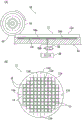
Fig. 1 is a perspective view schematically showing a configuration example of a workpiece (workpiece) 11 used in the present embodiment. As shown in fig. 1, the workpiece 11 is made of a semiconductor such as silicon (Si), gallium arsenide (GaAs), indium phosphide (InP), gallium nitride (GaN), or silicon carbide (SiC); sapphire (Al)2O3) Dielectrics (insulators) such as soda-lime glass, borosilicate glass, and quartz glass; or lithium tantalate (LiTaO)3) Lithium niobate (LiNbO)3) A disk-shaped wafer (substrate) formed of a ferroelectric substance (ferroelectric crystal) or the like.
The front surface 11a side of the workpiece 11 is divided into a plurality of regions 15 to be chips by a plurality of intersecting planned dividing lines (streets) 13. Hereinafter, a substantially circular region including all of the plurality of regions 15 to be chips is referred to as a chip region 11c, and a ring-shaped region surrounding the chip region 11c is referred to as an outer peripheral surplus region 11 d.
As necessary, devices such as an IC (Integrated Circuit), an MEMS (Micro Electro Mechanical Systems), an LED (Light Emitting Diode), an LD (Laser Diode), a Photodiode (Photodiode), a SAW (Surface Acoustic Wave) filter, and a BAW (Bulk Acoustic Wave) filter are formed in each region 15 in the chip region 11 c.
The workpiece 11 is divided along the lines to divide 13, thereby obtaining a plurality of chips. Specifically, when the workpiece 11 is a silicon wafer, a chip that functions as a memory, a sensor, or the like is obtained. When the workpiece 11 is a gallium arsenide substrate, an indium phosphide substrate, or a gallium nitride substrate, a chip functioning as a light-emitting element, a light-receiving element, or the like is obtained.
When the workpiece 11 is a silicon carbide substrate, a chip that functions as a power device or the like, for example, is obtained. When the workpiece 11 is a sapphire substrate, a chip functioning as a light-emitting element or the like is obtained, for example. When the workpiece 11 is a glass substrate made of soda-lime glass, borosilicate glass, quartz glass, or the like, a chip functioning as an optical member or a cover member (glass cover) is obtained, for example.
When the workpiece 11 is a ferroelectric substrate (ferroelectric crystal substrate) formed of a ferroelectric material such as lithium tantalate or lithium niobate, a chip functioning as a filter or an actuator, for example, is obtained. The material, shape, structure, size, thickness, and the like of the workpiece 11 are not limited. Similarly, the kind, number, shape, structure, size, arrangement, and the like of the devices formed in the region 15 to be a chip are not limited. Devices may not be formed in the region 15 to be a chip.
In the method for manufacturing a chip according to the present embodiment, a plurality of chips are manufactured using a disc-shaped silicon wafer as the workpiece 11. Specifically, first, a holding step is performed to directly hold the workpiece 11 by a chuck table. Fig. 2 is a perspective view schematically showing a configuration example of a laser processing apparatus used in the present embodiment.
As shown in fig. 2, the laser processing apparatus 2 includes a base 4 on which each component is mounted. A horizontal movement mechanism 8 is provided on the upper surface of the base 4, and the horizontal movement mechanism 8 moves a chuck table (holding table) 6 for sucking and holding a workpiece 11 in an X-axis direction (machining feed direction) and a Y-axis direction (indexing feed direction). The horizontal movement mechanism 8 includes a pair of X-axis guide rails 10 fixed to the upper surface of the base 4 and substantially parallel to the X-axis direction.
An X-axis moving table 12 is slidably attached to the X-axis guide rail 10. A nut portion (not shown) is provided on the back surface side (lower surface side) of the X-axis moving table 12, and an X-axis ball screw 14 substantially parallel to the X-axis guide rail 10 is screwed into the nut portion.
An X-axis pulse motor 16 is connected to one end of the X-axis ball screw 14. The X-axis ball screw 14 is rotated by the X-axis pulse motor 16, and the X-axis moving table 12 moves in the X-axis direction along the X-axis guide rail 10. An X-axis scale 18 is provided at a position adjacent to the X-axis guide rail 10, and the X-axis scale 18 is used to detect the position of the X-axis moving table 12 in the X-axis direction.
A pair of Y-axis guide rails 20 substantially parallel to the Y-axis direction are fixed to the front surface (upper surface) of the X-axis moving table 12. A Y-axis moving table 22 is slidably attached to the Y-axis guide rail 20. A nut portion (not shown) is provided on the back surface side (lower surface side) of the Y-axis moving table 22, and a Y-axis ball screw 24 substantially parallel to the Y-axis guide rail 20 is screwed to the nut portion.
A Y-axis pulse motor 26 is connected to one end of the Y-axis ball screw 24. The Y-axis moving table 22 is moved in the Y-axis direction along the Y-axis guide rail 20 by rotating the Y-axis ball screw 24 by the Y-axis pulse motor 26. A Y-axis scale 28 is provided adjacent to the Y-axis guide rail 20, and the Y-axis scale 28 detects the position of the Y-axis moving table 22 in the Y-axis direction.
A support table 30 is provided on the front side (upper surface side) of the Y-axis moving table 22, and a chuck table 6 is disposed above the support table 30. The front surface (upper surface) of the chuck table 6 serves as a holding surface 6a for sucking and holding the rear surface 11b side (or the front surface 11a side) of the workpiece 11. The holding surface 6a is made of a porous material having high hardness, such as alumina. However, the holding surface 6a may be made of a soft material such as polyethylene or a resin such as epoxy.
The holding surface 6a is connected to a suction source 34 (see fig. 3 a and the like) via a suction passage 6b (see fig. 3 a and the like) and a valve 32 (see fig. 3 a and the like) and the like formed inside the chuck table 6. A rotation drive source (not shown) is provided below the chuck table 6, and the chuck table 6 is rotated about a rotation axis substantially parallel to the Z-axis direction by the rotation drive source.
A columnar support structure 36 is provided behind the horizontal movement mechanism 8. A support arm 38 extending in the Y-axis direction is fixed to an upper portion of the support structure 36, and a laser irradiation unit 40 is provided at a distal end portion of the support arm 38, and the laser irradiation unit 40 pulse-oscillates the laser beam 17 (see fig. 3B) having a wavelength that is transparent to the workpiece 11 (a wavelength that is not easily absorbed) to irradiate the workpiece 11 on the chuck table 6.
A camera 42 is provided at a position adjacent to the laser irradiation unit 40, and the camera 42 images the front surface 11a side or the back surface 11b side of the workpiece 11. For example, when adjusting the positions of the workpiece 11 and the laser irradiation unit 40, an image formed by imaging the workpiece 11 and the like with the camera 42 is used.
The chuck table 6, the horizontal movement mechanism 8, the laser irradiation unit 40, the camera 42, and other components are connected to a control unit (not shown). The control unit controls each component so as to appropriately process the workpiece 11.
Fig. 3 (a) is a sectional view for explaining the holding step. In fig. 3 (a), some of the components are represented by functional blocks. In the holding step, as shown in fig. 3 (a), for example, the back surface 11b of the workpiece 11 is brought into contact with the holding surface 6a of the chuck table 6. Then, the valve 32 is opened, and the negative pressure of the suction source 34 is applied to the holding surface 6 a.
Thereby, the workpiece 11 is sucked and held on the chuck table 6 in a state where the front surface 11a side is exposed upward. In the present embodiment, as shown in fig. 3 (a), the back surface 11b side of the workpiece 11 is directly held by the chuck table 6. That is, in the present embodiment, it is not necessary to attach the extension sheet to the workpiece 11.
After the holding step, the 1 st and 2 nd laser processing steps are performed to irradiate the laser beam 17 having a wavelength that is transparent to the object 11 to form a modified layer along the lines to divide 13. In the present embodiment, a case where the 2 nd laser processing step is performed after the 1 st laser processing step will be described.
Fig. 3 (B) is a cross-sectional view for explaining the 1 st laser processing step and the 2 nd laser processing step, fig. 4 (a) is a plan view schematically showing the state of the workpiece 11 after the modified layer has been formed along all the lines to divide 13, and fig. 4 (B) is a cross-sectional view schematically showing the modified layer formed along each line to divide 13. In fig. 3 (B), some of the components are represented by functional blocks.
In the 1 st laser processing step, the chuck table 6 is first rotated so that, for example, the extending direction of the target line to be divided 13 is parallel to the X-axis direction. Next, the chuck table 6 is moved to align the position of the laser irradiation unit 40 on the extension line of the intended dividing line 13. Then, as shown in fig. 3 (B), the chuck table 6 is moved in the X-axis direction (i.e., the direction in which the target planned dividing line 13 extends).
Then, the laser beam 17 is irradiated from the laser irradiation unit 40 at a timing when the laser irradiation unit 40 reaches a position directly above one of the boundaries between the chip region 11c and the outer peripheral surplus region 11d, which are located at two positions on the line to divide 13 as the target. In the present embodiment, as shown in fig. 3 (B), the laser beam 17 is irradiated from the laser irradiation unit 40 disposed above the workpiece 11 toward the front surface 11a of the workpiece 11.
The irradiation of the laser beam 17 is continued until the laser irradiation unit 40 reaches a position directly above the other of the boundaries between the chip region 11c and the peripheral surplus region 11d, which are located at two positions on the line to divide 13 as the target. That is, here, the laser beam 17 is irradiated only in the chip region 11c along the line to divide the object 13.
The laser beam 17 is irradiated so that a focal point is positioned at a 1 st depth from the front surface 11a (or the rear surface 11b) inside the workpiece 11. By converging the laser beam 17 having a wavelength that is transparent to the workpiece 11 inside the workpiece 11 in this way, a part of the workpiece 11 can be modified by multiphoton absorption at the converging point and the vicinity thereof, and the modified layer 19 (the 1 st modified layer 19a) that is a starting point of division can be formed (the 1 st modified layer forming step).
In the 1 st laser processing step of the present embodiment, since the laser beam 17 is irradiated only within the chip region 11c along the line to divide the object 13, the modified layer 19 (the 1 st modified layer 19a) is formed only within the chip region 11c along the line to divide the object 13. That is, as shown in fig. 4B, in the 1 st laser processing step, the modified layer 19 (the 1 st modified layer 19a) is not formed in the outer peripheral residual region 11 d.
After the 1 st laser processing step, the 2 nd laser processing step is performed to form the modified layer 19 at a position having a depth different from the 1 st depth along the same line to divide 13. Further, since the laser irradiation unit 40 is present on the extension of the line to divide 13 as the target at the stage when the 1 st laser processing step is completed, it is not necessary to adjust the position of the laser irradiation unit 40 in accordance with the line to divide 13.
In the 2 nd laser processing step, first, the chuck table 6 is moved in the X-axis direction (the direction in which the line to divide the object 13 extends). Next, the laser beam 17 is irradiated from the laser irradiation unit 40 at a timing when the laser irradiation unit 40 reaches a position directly above the irradiation start point provided in the outer peripheral surplus region 11d of the workpiece 11.
In the present embodiment, as in the 1 st laser processing step, the laser beam 17 is irradiated from the laser irradiation unit 40 disposed above the workpiece 11 toward the front surface 11a of the workpiece 11. The irradiation of the laser beam 17 is continued until the laser irradiation unit 40 passes over the chip region 11c of the workpiece 11 and reaches a position immediately above an irradiation end point set in the outer peripheral residual region 11 d.
That is, here, the laser beam 17 is irradiated to a part of the outer peripheral surplus region 11d and the chip region 11c along the line to divide 13 of the object. The laser beam 17 is irradiated so that a focal point is positioned at a 2 nd depth (a depth different from the 1 st depth) from the front surface 11a (or the rear surface 11b) inside the workpiece 11.
Thereby, the modified layer 19 (the 2 nd modified layer 19b) can be formed at the 2 nd depth position along the line to divide 13, and the modified layer 19 (the 2 nd modified layer 19b) is longer than the modified layer 19 (the 1 st modified layer 19a) formed in the 1 st laser processing step and has an end portion overlapping the outer peripheral surplus region 11d (the 2 nd modified layer forming step). After the modified layer 19 (the 2 nd modified layer 19b) is formed at the 2 nd depth, the modified layer 19 (the 3 rd modified layer 19c) is formed at the 3 rd depth position different from the 1 st depth and the 2 nd depth in the same step (the 3 rd modified layer forming step). When the modified layer 19 is formed at the 3 rd depth position, the irradiation start point and the irradiation end point may be changed.
In the present embodiment, one modified layer 19 (1 st modified layer 19a) is formed along one line to divide 13 in the 1 st laser processing step, and two modified layers 19 (2 nd modified layer 19b and 3 rd modified layer 19c) are formed along the same line to divide 13 in the 2 nd laser processing step, but the number, position, and the like of the modified layers 19 formed along one line to divide 13 are not particularly limited.
For example, the number of the modified layers 19 formed along one line to divide 13 in the 1 st laser processing step may be two or more. In addition, the number of the modified layers 19 formed along the same line to divide 13 in the 2 nd laser processing step may be one or three or more. That is, at least in the 1 st laser processing step, one or more modified layers 19 may be formed along one line to divide 13, and at least in the 2 nd laser processing step, one or more modified layers 19 may be formed along one line to divide 13.
It is desirable to form the modified layer 19 under conditions such that the cracks reach the front surface 11a (or the back surface 11 b). Of course, the modified layer 19 may be formed under conditions such that the cracks reach both the front surface 11a and the back surface 11 b. This enables the workpiece 11 to be divided more appropriately.
When the workpiece 11 is a silicon wafer, the modified layer 19 is formed under the following conditions, for example.
The processed object is: silicon wafer
Wavelength of laser beam: 1340nm
Repetition frequency of laser beam: 90kHz
Output of laser beam: 0.1W-2W
Moving speed of chuck table (processing feed speed): 180mm/s to 1000mm/s, typically 500mm/s
When the workpiece 11 is a gallium arsenide substrate or an indium phosphide substrate, the modified layer 19 is formed under the following conditions, for example.
The processed object is: gallium arsenide substrate and indium phosphide substrate
Wavelength of laser beam: 1064nm
Repetition frequency of laser beam: 20kHz
Output of laser beam: 0.1W-2W
Moving speed of chuck table (processing feed speed): 100mm/s to 400mm/s, typically 200mm/s
When the workpiece 11 is a sapphire substrate, the modified layer 19 is formed under the following conditions, for example.
The processed object is: sapphire substrate
Wavelength of laser beam: 1045nm
Repetition frequency of laser beam: 100kHz
Output of laser beam: 0.1W-2W
Moving speed of chuck table (processing feed speed): 400mm/s to 800mm/s, typically 500mm/s
When the workpiece 11 is a ferroelectric substrate formed of a ferroelectric material such as lithium tantalate or lithium niobate, the modified layer 19 is formed under the following conditions, for example.
The processed object is: lithium tantalate substrate and lithium niobate substrate
Wavelength of laser beam: 532nm
Repetition frequency of laser beam: 15kHz
Output of laser beam: 0.02W-0.2W
Moving speed of chuck table (processing feed speed): 270mm/s to 420mm/s, typically 300mm/s
When the workpiece 11 is a glass substrate made of soda lime glass, borosilicate glass, quartz glass, or the like, the modified layer 19 is formed under the following conditions, for example.
The processed object is: soda-lime glass substrate, borosilicate glass substrate, and quartz glass substrate
Wavelength of laser beam: 532nm
Repetition frequency of laser beam: 50kHz
Output of laser beam: 0.1W-2W
Moving speed of chuck table (processing feed speed): 300mm/s to 600mm/s, typically 400mm/s
When the workpiece 11 is a gallium nitride substrate, the modified layer 19 is formed under the following conditions, for example.
The processed object is: gallium nitride substrate
Wavelength of laser beam: 532nm
Repetition frequency of laser beam: 25kHz
Output of laser beam: 0.02W-0.2W
Moving speed of chuck table (processing feed speed): 90mm/s to 600mm/s, typically 150mm/s
When the workpiece 11 is a silicon carbide substrate, the modified layer 19 is formed under the following conditions, for example.
The processed object is: silicon carbide substrate
Wavelength of laser beam: 532nm
Repetition frequency of laser beam: 25kHz
Output of laser beam: 0.02W to 0.2W, typically 0.1W
Moving speed of chuck table (processing feed speed): 90mm/s to 600mm/s, typically: 90mm/s in the cleavage direction of the silicon carbide substrate and 400mm/s in the non-cleavage direction
After the modified layer 19 is formed along the lines to divide 13, the above-described 1 st and 2 nd laser processing steps are repeated for all the lines to divide 13 remaining. As a result, as shown in fig. 4 (a), the modified layer 19 can be formed along all the lines to divide 13.
In the 1 st laser processing step of the present embodiment, the modified layer 19 (the 1 st modified layer 19a) is formed only in the chip region 11c along the line to divide 13, and the modified layer 19 (the 1 st modified layer 19a) is not formed in the outer periphery-remaining region 11d, so that the strength of the workpiece 11 is secured by the outer periphery-remaining region 11 d. This prevents the workpiece 11 from being divided into individual chips by a force applied during conveyance or the like. In this way, the outer peripheral surplus region 11d after the 1 st laser processing step functions as a reinforcing portion for reinforcing the chip region 11.
In addition, since the modified layer 19 (the 1 st modified layer 19a) is not formed in the outer peripheral excess region 11d in the 1 st laser processing step of the present embodiment, even in a state where, for example, a crack extending from the modified layer 19 reaches both the front surface 11a and the back surface 11b and the workpiece 11 is completely divided, the chips are not detached or scattered. In general, when the modified layer 19 is formed in the workpiece 11, the workpiece 11 expands in the vicinity of the modified layer 19. In the present embodiment, the annular outer peripheral surplus region 11d functioning as the reinforcing portion inwardly acts a force of expansion caused by the formation of the modified layer 19, and the chips are pressed against each other to prevent the chips from falling off or scattering.
After the 1 st and 2 nd laser processing steps, a carrying-out step is performed to carry out the object 11 from the chuck table 6. Specifically, for example, the entire front surface 11a of the workpiece 11 is sucked by a conveying means (not shown) capable of sucking and holding the entire front surface 11a (or the rear surface 11b) of the workpiece 11, and then the workpiece 11 is carried out by closing the valve 32, cutting off the negative pressure of the suction source 34. In the present embodiment, since the outer peripheral surplus region 11d functions as the reinforcement portion as described above, the workpiece 11 is not divided into individual chips by the force applied during conveyance or the like, and the workpiece 11 can be appropriately conveyed.
After the carrying-out step, a reinforcement removing step is performed to remove the reinforcement from the workpiece 11. Fig. 5 (a) and 5 (B) are cross-sectional views for explaining the reinforcing part removing step. In fig. 5 (a) and 5 (B), some of the components are represented by functional blocks. The reinforcing part removing step is performed using, for example, a dividing device 52 shown in fig. 5 (a) and 5 (B).
The dividing device 52 has a chuck table (holding table) 54 for sucking and holding the workpiece 11. A part of the upper surface of the chuck table 54 serves as a holding surface 54a for sucking and holding the chip region 11c of the workpiece 11. The holding surface 54a is connected to a suction source 58 via a suction passage 54b and a valve 56 formed inside the chuck table 54. A heater (heating means) 54c is disposed below the holding surface 54 a.
One end of a suction path 54d for sucking and holding the outer peripheral surplus region 11d (i.e., the reinforcing portion) of the workpiece 11 is opened to another part of the upper surface of the chuck table 54. The other end side of the suction passage 54d is connected to a suction source 58 via a valve 60 and the like. The chuck table 54 is connected to a rotation driving source (not shown) such as a motor, and rotates about a rotation axis substantially parallel to the vertical direction.
A cutting unit 62 is disposed above the chuck table 54. The cutting unit 62 has a spindle 64 as a rotation axis substantially parallel to the holding surface 54 a. An annular cutting tool 66 having abrasive grains dispersed in a binder is attached to one end of the spindle 64.
A rotary drive source (not shown) such as a motor is connected to the other end side of the spindle 64, and the cutting tool 66 attached to one end side of the spindle 64 is rotated by a force transmitted from the rotary drive source. The cutting unit 62 is supported by, for example, an elevating mechanism (not shown), and the cutting tool 66 is moved in the vertical direction by the elevating mechanism.
Further, a relief groove (not shown) for a cutting tool for preventing contact with the cutting tool 66 is formed on the upper surface of the chuck table 54 at a position corresponding to the boundary between the chip region 11c and the outer peripheral surplus region 11d of the workpiece 11.
In the reinforcement portion removing step, first, the back surface 11b of the workpiece 11 is brought into contact with the holding surface 54a of the chuck table 54. Then, the valves 56 and 60 are opened, and the negative pressure of the suction source 58 is applied to the holding surface 54a and the like. Thereby, the workpiece 11 is sucked and held by the chuck table 54 in a state where the front surface 11a side is exposed upward. In the present embodiment, as shown in fig. 5 (a), the back surface 11b side of the workpiece 11 is directly held by the chuck table 54. That is, here too, it is not necessary to attach an expansion sheet to the workpiece 11.
Next, the cutting tool 66 is rotated to cut into the boundary between the chip region 11c and the outer peripheral residual region 11d of the workpiece 11. At the same time, as shown in fig. 5 (a), the chuck table 54 is rotated about a rotation axis substantially parallel to the vertical direction. Thereby, the workpiece 11 can be cut along the boundary between the chip region 11c and the outer peripheral surplus region 11 d.
Then, the valve 60 is closed, and the negative pressure applied from the suction source 58 to the outer peripheral surplus region 11d of the workpiece 11 is blocked. Then, as shown in fig. 5 (B), the outer peripheral residual region 11d is removed from the chuck table 54. Thereby, only the chip region 11c of the workpiece 11 remains on the chuck table 54.
After the reinforcement portion removing step, a dividing step is performed to divide the workpiece 11 into individual chips. Specifically, the workpiece 11 is divided by heating and cooling to generate stress. Fig. 6 is a sectional view for explaining the dividing step. In fig. 6, some of the components are represented by functional blocks.
The splitting step continues using the splitting means 52. As shown in fig. 6, the dividing device 52 further includes a nozzle (cooling unit) 68 disposed above the chuck table 54. In the dividing step of the present embodiment, after the workpiece 11 is heated by the heater 54c provided on the chuck table 54, the cooling fluid 21 is supplied from the nozzle 68 to cool the workpiece 11, and the stress necessary for dividing the workpiece 11 is generated.
As the fluid 21 for cooling, for example, a liquid such as water or a gas such as air can be used. In the case of using a liquid as the fluid 21, the liquid may be cooled to a low temperature (for example, a temperature of about 0.1 to 10 ℃ higher than the freezing point) in advance to such an extent that the liquid is not frozen. However, the type, flow rate, temperature, and the like of the fluid 21 are not particularly limited. For example, a low-temperature liquid such as liquid nitrogen that can absorb heat further by vaporization may be used.
When the workpiece 11 is heated by operating the heater 54c and then cooled by supplying the cooling fluid 21 from the nozzle 68, the crack 23 extends from the modified layer 19 due to the stress generated in the workpiece 11. Thereby, the workpiece 11 is divided into the plurality of chips 25 along the lines to divide 13.
The conditions (temperature, time, etc.) for heating and cooling are set according to the type of the workpiece 11. It is desirable to repeat heating of the workpiece 11 by the heater 54c and cooling of the workpiece 11 by the liquid 21 supplied from the nozzle 68 until the workpiece 11 can be appropriately divided.
In this way, in the present embodiment, the workpiece 11 can be divided into the respective chips 25 by applying a necessary force by heating and cooling. In the present embodiment, the workpiece 11 is heated and then cooled, but the workpiece 11 may be cooled and then heated. There is also no particular limitation on the method of heating and cooling.
As described above, in the method of manufacturing chips according to the present embodiment, in a state where the object (workpiece) 11 is directly held by the chuck table (holding table) 6, the modified layer 19 (1 st modified layer 19a) is formed along the planned dividing line 13 of the device region 11c by irradiating only the chip region 11c of the object 11 with the laser beam 17 so as to position the light converging point at the 1 st depth, and the modified layers 19 (2 nd modified layer 19b and 3 rd modified layer 19c) are formed along the planned dividing line 13 by irradiating the laser beam 17 so as to position the light converging point at the 2 nd depth and the 3 rd depth, the modified layers 19 (2 nd modified layer 19b and 3 rd modified layer 19c) being longer than the modified layer 19 formed at the 1 st depth and having the end portions overlapping the outer peripheral remaining region 11d, and then applying a force by heating and cooling to divide the object 11 into the chips 25, therefore, it is not necessary to use an expansion sheet for dividing the workpiece 11 into the chips 25. As described above, according to the chip manufacturing method of the present embodiment, the silicon wafer, which is the plate-shaped workpiece 11, can be divided without using the extending sheet to manufacture the plurality of chips 25.
In the chip manufacturing method according to the present embodiment, the modified layer 19 (the 1 st modified layer 19a) along the lines to divide 13 is formed by irradiating only the chip region 11c of the workpiece 11 with the laser beam 17, and the chip region 11c is reinforced by the reinforcing portion since the outer peripheral excess region 11d is the reinforcing portion where the modified layer 19 is not formed. This prevents the workpiece 11 from being divided into the chips 25 by a force applied during conveyance or the like, and the workpiece 11 can be appropriately conveyed.
The present invention is not limited to the above-described embodiments, and can be implemented with various modifications. For example, in the above embodiment, the 2 nd laser processing step is performed after the 1 st laser processing step, but the 1 st laser processing step may be performed after the 2 nd laser processing step. In addition, the order of the 2 nd modified layer forming step of forming the 2 nd modified layer 19b and the 3 rd modified layer forming step of forming the 3 rd modified layer 19c may be changed.
In the above embodiment, the 1 st laser processing is performed on one intended line 13 and then the 2 nd laser processing step is performed on the same intended line 13, but the present invention is not limited to this form. For example, after the 1 st laser processing step (the 1 st modified layer forming step) of forming the 1 st modified layer 19a is performed on the plurality of lines to divide 13, the 2 nd laser processing step may be performed on the plurality of lines to divide 13.
In this case, after the 2 nd laser processing step (the 2 nd modified layer forming step) of forming the 2 nd modified layer 19b is performed on the plurality of lines to divide 13, the 2 nd laser processing step (the 3 rd modified layer forming step) of forming the 3 rd modified layer 19c may be performed on the plurality of lines to divide 13.
More specifically, for example, the 1 st modified layer forming step of forming the 1 st modified layer 19a is first performed on all the lines to divide 13 parallel to the 1 st direction. Next, a 2 nd modified layer forming step of forming a 2 nd modified layer 19b is performed on all the lines to divide 13 parallel to the 1 st direction. Then, a 3 rd modified layer forming step of forming a 3 rd modified layer 19c is performed for all the lines to divide 13 parallel to the 1 st direction.
Then, a 1 st modified layer forming step of forming a 1 st modified layer 19a is performed on all the lines to divide 13 parallel to a 2 nd direction different from the 1 st direction. Next, a 2 nd modified layer forming step of forming a 2 nd modified layer 19b is performed on all the lines to divide 13 parallel to the 2 nd direction. Then, a 3 rd modified layer forming step of forming a 3 rd modified layer 19c is performed for all the lines to divide 13 parallel to the 2 nd direction.
In this case, the 1 st laser processing step (1 st modified layer forming step) may be performed after the 2 nd laser processing step (2 nd modified layer forming step and 3 rd modified layer forming step). Similarly, the order of the 2 nd modified layer forming step of forming the 2 nd modified layer 19b and the 3 rd modified layer forming step of forming the 3 rd modified layer 19c may be changed.
In the above embodiment, the laser beam 17 is directly held by the chuck table 6 on the back surface 11b side of the workpiece 11 and irradiated from the front surface 11a side, but the laser beam 17 may be directly held by the chuck table 6 on the front surface 11a side of the workpiece 11 and irradiated from the back surface 11b side.
Fig. 7 is a sectional view for explaining a holding step of a modification. In the holding step of this modification, as shown in fig. 7, a chuck table (holding table) 6 whose upper surface is formed of a porous sheet material (porous sheet material) 44 made of a soft material such as polyethylene or a resin such as epoxy, for example, may be used.
In the chuck table 6, the front surface 11a side of the workpiece 11 is sucked and held by the upper surface 44a of the sheet 44. This can prevent the devices and the like formed on the front surface 11a from being damaged. The sheet 44 is a part of the chuck table 6, and is reused together with a main body of the chuck table 6 and the like.
However, the upper surface of the chuck table 6 does not need to be formed of the porous sheet 44, and may be formed of a flexible material at least to such an extent that the devices and the like formed on the front surface 11a side of the workpiece 11 are not damaged. Further, it is desirable that the sheet 44 is configured to be attachable to and detachable from the main body of the chuck table 6, and to be replaceable in the case of breakage or the like.
In the above embodiment, the reinforcing part removing step is performed after the carrying-out step and before the dividing step, but the reinforcing part removing step may be performed after the 1 st laser processing step and the 2 nd laser processing step and before the carrying-out step, for example. In addition, when the reinforcement removal step is performed after the carry-out step and before the dividing step, it is not necessary to carry the workpiece 11 after the reinforcement removal step, and therefore it is easy to avoid a problem that the workpiece 11 cannot be carried appropriately, or the like.
In addition, the reinforcement removing step may be omitted. In the 2 nd laser processing step of the above embodiment, the modified layers 19 (the 2 nd modified layer 19b and the 3 rd modified layer 19c) having ends overlapping the outer peripheral residual region 11d are formed along the lines to divide 13. Therefore, the outer peripheral surplus region 11d is easily divided, as compared with the case where the modified layer 19 does not overlap with the outer peripheral surplus region 11 d. Thus, the chip region 11c and the outer peripheral surplus region 11d can be divided together in the dividing step without performing the reinforcement portion removing step.
In this case, for example, the range of forming the modified layer 19 in the 2 nd laser processing step may be adjusted so that the distance from the outer peripheral edge of the workpiece 11 to one end of the modified layer 19 is about 2mm to 3 mm. For example, a groove may be formed as a starting point of division in the reinforcing portion before the chip region 11c is divided in the dividing step. Fig. 8 (a) is a cross-sectional view for explaining a dividing step of the modification, and fig. 8 (B) is a plan view schematically showing a state of the workpiece 11 after the dividing step of the modification.
In the dividing step of the modified example, as shown in fig. 8 a and 8B, the cutting tool 66 is cut into the outer peripheral surplus region 11d (i.e., the reinforcing portion), thereby forming the groove 11e as a starting point of the division. The groove 11e is desirably formed along the line to divide 13, for example. By forming such grooves 11e, the workpiece 11 can be divided into the outer peripheral surplus regions 11d by thermal shock. In the dividing step of the modification, the suction passage 54d of the chuck table 54, the valve 60, and the like may be omitted.
In addition, the structures, methods, and the like of the above-described embodiments and modifications may be appropriately modified and implemented without departing from the scope of the object of the present invention.
Claims (3)
1. A method of manufacturing a chip, which manufactures a plurality of chips from a work having a chip region and a peripheral surplus region surrounding the chip region, the chip region being divided into a plurality of regions to be the chips by a plurality of division scheduled lines which intersect,
the method for manufacturing the chip is characterized by comprising the following steps:
a holding step of directly holding the workpiece by using a holding table;
a 1 st laser processing step of, after the holding step is performed, irradiating only the chip region of the workpiece along a planned dividing line with a laser beam having a wavelength that is transparent to the workpiece so that a condensing point of the laser beam is positioned at a 1 st depth position inside the workpiece held by the holding table, forming a 1 st modified layer along the planned dividing line of the chip region, and setting the peripheral residual region as a reinforcing portion where the 1 st modified layer is not formed;
a 2 nd laser processing step of, after the holding step is performed, irradiating the laser beam along the planned dividing line so that a converging point of the laser beam having a wavelength that is transparent to the workpiece is positioned at a 2 nd depth position different from the 1 st depth in the workpiece held by the holding table, and forming a 2 nd modified layer along the planned dividing line, the 2 nd modified layer being longer than the 1 st modified layer and having an end portion overlapping the outer peripheral residual region;
a carrying-out step of carrying out the object to be processed from the holding table after the 1 st and 2 nd laser processing steps are performed; and
a dividing step of dividing the workpiece into the chips by applying a force to the workpiece after the carrying out step,
in the dividing step, the workpiece is heated and then cooled, or the workpiece is cooled and then heated, whereby the force is applied by heating and cooling without using an expansion sheet, thereby dividing the workpiece into the chips.
2. The method of manufacturing a chip according to claim 1,
the method for manufacturing the chip further comprises the following reinforcing part removing step: the reinforcement portion is removed after the 1 st and 2 nd laser processing steps are performed and before the dividing step is performed.
3. The method of manufacturing a chip according to claim 1 or 2,
the upper surface of the holding table is made of a soft material,
in the holding step, the front surface side of the workpiece is held by the soft material.
Applications Claiming Priority (2)
| Application Number | Priority Date | Filing Date | Title |
|---|---|---|---|
| JP2017182986A JP6896344B2 (en) | 2017-09-22 | 2017-09-22 | Chip manufacturing method |
| JP2017-182986 | 2017-09-22 |
Publications (2)
| Publication Number | Publication Date |
|---|---|
| CN109531838A CN109531838A (en) | 2019-03-29 |
| CN109531838B true CN109531838B (en) | 2021-12-21 |
Family
ID=65838977
Family Applications (1)
| Application Number | Title | Priority Date | Filing Date |
|---|---|---|---|
| CN201811080404.0A Active CN109531838B (en) | 2017-09-22 | 2018-09-17 | Method for manufacturing chip |
Country Status (4)
| Country | Link |
|---|---|
| JP (1) | JP6896344B2 (en) |
| KR (1) | KR102578958B1 (en) |
| CN (1) | CN109531838B (en) |
| TW (1) | TWI770280B (en) |
Families Citing this family (1)
| Publication number | Priority date | Publication date | Assignee | Title |
|---|---|---|---|---|
| TWI733604B (en) * | 2020-06-10 | 2021-07-11 | 財團法人工業技術研究院 | Laser processing system and method for glass workpiece |
Citations (20)
| Publication number | Priority date | Publication date | Assignee | Title |
|---|---|---|---|---|
| CN1590007A (en) * | 2003-09-01 | 2005-03-09 | 株式会社东芝 | Apparatus for laser beam machining, machining mask, method for laser beam machining, method for manufacturing a semiconductor device and semiconductor device |
| JP2007019379A (en) * | 2005-07-11 | 2007-01-25 | Disco Abrasive Syst Ltd | Method for processing wafer |
| CN1967805A (en) * | 2005-11-16 | 2007-05-23 | 株式会社电装 | Semiconductor device and dicing method for semiconductor substrate |
| CN101073145A (en) * | 2004-12-08 | 2007-11-14 | 雷射先进科技株式会社 | Division starting poin forming method in body to be divided, dividing method for body to be divided, and method of processing work by pulse laser beam |
| CN101146642A (en) * | 2005-03-22 | 2008-03-19 | 浜松光子学株式会社 | Laser machining method |
| CN102024753A (en) * | 2009-09-10 | 2011-04-20 | 株式会社迪思科 | Laser processing method for workpiece |
| CN102326232A (en) * | 2009-02-25 | 2012-01-18 | 日亚化学工业株式会社 | Semiconductor element manufacturing method |
| JP2012054275A (en) * | 2010-08-31 | 2012-03-15 | Disco Abrasive Syst Ltd | Wafer processing method |
| CN102626835A (en) * | 2011-02-04 | 2012-08-08 | 三星钻石工业股份有限公司 | Laser scribe method and laser processing apparatus |
| CN103177943A (en) * | 2011-12-26 | 2013-06-26 | 株式会社迪思科 | Laser processing method for wafer |
| JP2013152987A (en) * | 2012-01-24 | 2013-08-08 | Disco Abrasive Syst Ltd | Method for processing wafer |
| JP2013236001A (en) * | 2012-05-10 | 2013-11-21 | Disco Abrasive Syst Ltd | Method for dividing plate-like object |
| JP2014199834A (en) * | 2013-03-29 | 2014-10-23 | 株式会社ディスコ | Holding means and processing method |
| CN105665947A (en) * | 2014-12-04 | 2016-06-15 | 株式会社迪思科 | Wafer producing method |
| CN105750742A (en) * | 2015-01-06 | 2016-07-13 | 株式会社迪思科 | Wafer producing method |
| CN106057737A (en) * | 2015-04-15 | 2016-10-26 | 株式会社迪思科 | Sheet separation method |
| CN106216858A (en) * | 2015-06-02 | 2016-12-14 | 株式会社迪思科 | The generation method of wafer |
| CN106328778A (en) * | 2016-09-14 | 2017-01-11 | 中国科学院半导体研究所 | Method of preparing LED chips with upright, inverted and inverted trapezoidal substrates through invisible cutting |
| CN106469679A (en) * | 2015-08-18 | 2017-03-01 | 株式会社迪思科 | The processing method of chip |
| CN106914697A (en) * | 2011-01-13 | 2017-07-04 | 浜松光子学株式会社 | Laser processing |
Family Cites Families (15)
| Publication number | Priority date | Publication date | Assignee | Title |
|---|---|---|---|---|
| JPS5939769B2 (en) * | 1981-03-27 | 1984-09-26 | 昭和情報機器株式会社 | input device |
| JP4659300B2 (en) * | 2000-09-13 | 2011-03-30 | 浜松ホトニクス株式会社 | Laser processing method and semiconductor chip manufacturing method |
| JP3408805B2 (en) | 2000-09-13 | 2003-05-19 | 浜松ホトニクス株式会社 | Cutting origin region forming method and workpiece cutting method |
| US20060030156A1 (en) * | 2004-08-05 | 2006-02-09 | Applied Materials, Inc. | Abrasive conductive polishing article for electrochemical mechanical polishing |
| JP5791866B2 (en) | 2009-03-06 | 2015-10-07 | 株式会社ディスコ | Work dividing device |
| KR20130033114A (en) * | 2011-09-26 | 2013-04-03 | 주식회사 이오테크닉스 | Laser processing method |
| JP5939769B2 (en) | 2011-11-11 | 2016-06-22 | 株式会社ディスコ | Processing method of plate |
| JP2014236034A (en) * | 2013-05-31 | 2014-12-15 | 株式会社ディスコ | Method for processing wafer |
| US9236284B2 (en) * | 2014-01-31 | 2016-01-12 | Applied Materials, Inc. | Cooled tape frame lift and low contact shadow ring for plasma heat isolation |
| CN105171235B (en) * | 2014-06-23 | 2018-06-01 | 大族激光科技产业集团股份有限公司 | A kind of double focus laser micromachining device and its processing method |
| JP6472347B2 (en) * | 2015-07-21 | 2019-02-20 | 株式会社ディスコ | Thinning method of wafer |
| PL3334697T3 (en) * | 2015-08-10 | 2022-01-24 | Saint-Gobain Glass France | Method for cutting a thin glass layer |
| JP6504977B2 (en) | 2015-09-16 | 2019-04-24 | 株式会社ディスコ | Wafer processing method |
| JP6605278B2 (en) | 2015-09-29 | 2019-11-13 | 浜松ホトニクス株式会社 | Laser processing method |
| JP2017107903A (en) * | 2015-12-07 | 2017-06-15 | 株式会社ディスコ | Processing method of wafer |
-
2017
- 2017-09-22 JP JP2017182986A patent/JP6896344B2/en active Active
-
2018
- 2018-09-06 KR KR1020180106688A patent/KR102578958B1/en active IP Right Grant
- 2018-09-17 CN CN201811080404.0A patent/CN109531838B/en active Active
- 2018-09-19 TW TW107133067A patent/TWI770280B/en active
Patent Citations (20)
| Publication number | Priority date | Publication date | Assignee | Title |
|---|---|---|---|---|
| CN1590007A (en) * | 2003-09-01 | 2005-03-09 | 株式会社东芝 | Apparatus for laser beam machining, machining mask, method for laser beam machining, method for manufacturing a semiconductor device and semiconductor device |
| CN101073145A (en) * | 2004-12-08 | 2007-11-14 | 雷射先进科技株式会社 | Division starting poin forming method in body to be divided, dividing method for body to be divided, and method of processing work by pulse laser beam |
| CN101146642A (en) * | 2005-03-22 | 2008-03-19 | 浜松光子学株式会社 | Laser machining method |
| JP2007019379A (en) * | 2005-07-11 | 2007-01-25 | Disco Abrasive Syst Ltd | Method for processing wafer |
| CN1967805A (en) * | 2005-11-16 | 2007-05-23 | 株式会社电装 | Semiconductor device and dicing method for semiconductor substrate |
| CN102326232A (en) * | 2009-02-25 | 2012-01-18 | 日亚化学工业株式会社 | Semiconductor element manufacturing method |
| CN102024753A (en) * | 2009-09-10 | 2011-04-20 | 株式会社迪思科 | Laser processing method for workpiece |
| JP2012054275A (en) * | 2010-08-31 | 2012-03-15 | Disco Abrasive Syst Ltd | Wafer processing method |
| CN106914697A (en) * | 2011-01-13 | 2017-07-04 | 浜松光子学株式会社 | Laser processing |
| CN102626835A (en) * | 2011-02-04 | 2012-08-08 | 三星钻石工业股份有限公司 | Laser scribe method and laser processing apparatus |
| CN103177943A (en) * | 2011-12-26 | 2013-06-26 | 株式会社迪思科 | Laser processing method for wafer |
| JP2013152987A (en) * | 2012-01-24 | 2013-08-08 | Disco Abrasive Syst Ltd | Method for processing wafer |
| JP2013236001A (en) * | 2012-05-10 | 2013-11-21 | Disco Abrasive Syst Ltd | Method for dividing plate-like object |
| JP2014199834A (en) * | 2013-03-29 | 2014-10-23 | 株式会社ディスコ | Holding means and processing method |
| CN105665947A (en) * | 2014-12-04 | 2016-06-15 | 株式会社迪思科 | Wafer producing method |
| CN105750742A (en) * | 2015-01-06 | 2016-07-13 | 株式会社迪思科 | Wafer producing method |
| CN106057737A (en) * | 2015-04-15 | 2016-10-26 | 株式会社迪思科 | Sheet separation method |
| CN106216858A (en) * | 2015-06-02 | 2016-12-14 | 株式会社迪思科 | The generation method of wafer |
| CN106469679A (en) * | 2015-08-18 | 2017-03-01 | 株式会社迪思科 | The processing method of chip |
| CN106328778A (en) * | 2016-09-14 | 2017-01-11 | 中国科学院半导体研究所 | Method of preparing LED chips with upright, inverted and inverted trapezoidal substrates through invisible cutting |
Also Published As
| Publication number | Publication date |
|---|---|
| JP2019061980A (en) | 2019-04-18 |
| TWI770280B (en) | 2022-07-11 |
| KR20190034085A (en) | 2019-04-01 |
| JP6896344B2 (en) | 2021-06-30 |
| CN109531838A (en) | 2019-03-29 |
| TW201916138A (en) | 2019-04-16 |
| KR102578958B1 (en) | 2023-09-14 |
Similar Documents
| Publication | Publication Date | Title |
|---|---|---|
| CN109531838B (en) | Method for manufacturing chip | |
| CN108987339B (en) | Method for manufacturing chip | |
| CN108987341B (en) | Method for manufacturing chip | |
| JP6851691B2 (en) | Chip manufacturing method | |
| JP6925721B2 (en) | Chip manufacturing method | |
| JP6851690B2 (en) | Chip manufacturing method | |
| JP6925720B2 (en) | Chip manufacturing method | |
| CN110473831B (en) | Method for manufacturing chip | |
| CN110491784B (en) | Method for manufacturing chip | |
| JP2019040910A (en) | Chip manufacturing method | |
| JP2019059628A (en) | Method of manufacturing chip | |
| JP6851692B2 (en) | Chip manufacturing method | |
| JP6903379B2 (en) | Chip manufacturing method | |
| JP6918423B2 (en) | Chip manufacturing method | |
| JP6918424B2 (en) | Chip manufacturing method | |
| JP6903378B2 (en) | Chip manufacturing method | |
| JP6918422B2 (en) | Chip manufacturing method | |
| JP6925722B2 (en) | Chip manufacturing method | |
| JP2019197861A (en) | Chip manufacturing method | |
| JP2019197864A (en) | Chip manufacturing method | |
| JP2019038703A (en) | Method for manufacturing chip | |
| JP2019197860A (en) | Chip manufacturing method | |
| JP2019197862A (en) | Chip manufacturing method | |
| JP2019040912A (en) | Chip manufacturing method | |
| JP2019197863A (en) | Chip manufacturing method |
Legal Events
| Date | Code | Title | Description |
|---|---|---|---|
| PB01 | Publication | ||
| PB01 | Publication | ||
| SE01 | Entry into force of request for substantive examination | ||
| SE01 | Entry into force of request for substantive examination | ||
| GR01 | Patent grant | ||
| GR01 | Patent grant |