JP6896344B2 - Chip manufacturing method - Google Patents
Chip manufacturing method Download PDFInfo
- Publication number
- JP6896344B2 JP6896344B2 JP2017182986A JP2017182986A JP6896344B2 JP 6896344 B2 JP6896344 B2 JP 6896344B2 JP 2017182986 A JP2017182986 A JP 2017182986A JP 2017182986 A JP2017182986 A JP 2017182986A JP 6896344 B2 JP6896344 B2 JP 6896344B2
- Authority
- JP
- Japan
- Prior art keywords
- workpiece
- modified layer
- chip
- holding
- laser beam
- Prior art date
- Legal status (The legal status is an assumption and is not a legal conclusion. Google has not performed a legal analysis and makes no representation as to the accuracy of the status listed.)
- Active
Links
Images


Classifications
-
- B—PERFORMING OPERATIONS; TRANSPORTING
- B28—WORKING CEMENT, CLAY, OR STONE
- B28D—WORKING STONE OR STONE-LIKE MATERIALS
- B28D5/00—Fine working of gems, jewels, crystals, e.g. of semiconductor material; apparatus or devices therefor
- B28D5/0005—Fine working of gems, jewels, crystals, e.g. of semiconductor material; apparatus or devices therefor by breaking, e.g. dicing
- B28D5/0011—Fine working of gems, jewels, crystals, e.g. of semiconductor material; apparatus or devices therefor by breaking, e.g. dicing with preliminary treatment, e.g. weakening by scoring
-
- H—ELECTRICITY
- H01—ELECTRIC ELEMENTS
- H01L—SEMICONDUCTOR DEVICES NOT COVERED BY CLASS H10
- H01L21/00—Processes or apparatus adapted for the manufacture or treatment of semiconductor or solid state devices or of parts thereof
- H01L21/70—Manufacture or treatment of devices consisting of a plurality of solid state components formed in or on a common substrate or of parts thereof; Manufacture of integrated circuit devices or of parts thereof
- H01L21/77—Manufacture or treatment of devices consisting of a plurality of solid state components or integrated circuits formed in, or on, a common substrate
- H01L21/78—Manufacture or treatment of devices consisting of a plurality of solid state components or integrated circuits formed in, or on, a common substrate with subsequent division of the substrate into plural individual devices
-
- B—PERFORMING OPERATIONS; TRANSPORTING
- B23—MACHINE TOOLS; METAL-WORKING NOT OTHERWISE PROVIDED FOR
- B23K—SOLDERING OR UNSOLDERING; WELDING; CLADDING OR PLATING BY SOLDERING OR WELDING; CUTTING BY APPLYING HEAT LOCALLY, e.g. FLAME CUTTING; WORKING BY LASER BEAM
- B23K26/00—Working by laser beam, e.g. welding, cutting or boring
- B23K26/36—Removing material
- B23K26/38—Removing material by boring or cutting
-
- B—PERFORMING OPERATIONS; TRANSPORTING
- B24—GRINDING; POLISHING
- B24B—MACHINES, DEVICES, OR PROCESSES FOR GRINDING OR POLISHING; DRESSING OR CONDITIONING OF ABRADING SURFACES; FEEDING OF GRINDING, POLISHING, OR LAPPING AGENTS
- B24B27/00—Other grinding machines or devices
- B24B27/06—Grinders for cutting-off
- B24B27/0675—Grinders for cutting-off methods therefor
-
- B—PERFORMING OPERATIONS; TRANSPORTING
- B28—WORKING CEMENT, CLAY, OR STONE
- B28D—WORKING STONE OR STONE-LIKE MATERIALS
- B28D5/00—Fine working of gems, jewels, crystals, e.g. of semiconductor material; apparatus or devices therefor
- B28D5/0005—Fine working of gems, jewels, crystals, e.g. of semiconductor material; apparatus or devices therefor by breaking, e.g. dicing
-
- H—ELECTRICITY
- H01—ELECTRIC ELEMENTS
- H01L—SEMICONDUCTOR DEVICES NOT COVERED BY CLASS H10
- H01L21/00—Processes or apparatus adapted for the manufacture or treatment of semiconductor or solid state devices or of parts thereof
- H01L21/02—Manufacture or treatment of semiconductor devices or of parts thereof
- H01L21/04—Manufacture or treatment of semiconductor devices or of parts thereof the devices having at least one potential-jump barrier or surface barrier, e.g. PN junction, depletion layer or carrier concentration layer
- H01L21/18—Manufacture or treatment of semiconductor devices or of parts thereof the devices having at least one potential-jump barrier or surface barrier, e.g. PN junction, depletion layer or carrier concentration layer the devices having semiconductor bodies comprising elements of Group IV of the Periodic System or AIIIBV compounds with or without impurities, e.g. doping materials
- H01L21/30—Treatment of semiconductor bodies using processes or apparatus not provided for in groups H01L21/20 - H01L21/26
- H01L21/302—Treatment of semiconductor bodies using processes or apparatus not provided for in groups H01L21/20 - H01L21/26 to change their surface-physical characteristics or shape, e.g. etching, polishing, cutting
- H01L21/304—Mechanical treatment, e.g. grinding, polishing, cutting
- H01L21/3043—Making grooves, e.g. cutting
-
- H—ELECTRICITY
- H01—ELECTRIC ELEMENTS
- H01L—SEMICONDUCTOR DEVICES NOT COVERED BY CLASS H10
- H01L21/00—Processes or apparatus adapted for the manufacture or treatment of semiconductor or solid state devices or of parts thereof
- H01L21/02—Manufacture or treatment of semiconductor devices or of parts thereof
- H01L21/04—Manufacture or treatment of semiconductor devices or of parts thereof the devices having at least one potential-jump barrier or surface barrier, e.g. PN junction, depletion layer or carrier concentration layer
- H01L21/50—Assembly of semiconductor devices using processes or apparatus not provided for in a single one of the subgroups H01L21/06 - H01L21/326, e.g. sealing of a cap to a base of a container
- H01L21/56—Encapsulations, e.g. encapsulation layers, coatings
-
- H—ELECTRICITY
- H01—ELECTRIC ELEMENTS
- H01L—SEMICONDUCTOR DEVICES NOT COVERED BY CLASS H10
- H01L21/00—Processes or apparatus adapted for the manufacture or treatment of semiconductor or solid state devices or of parts thereof
- H01L21/67—Apparatus specially adapted for handling semiconductor or electric solid state devices during manufacture or treatment thereof; Apparatus specially adapted for handling wafers during manufacture or treatment of semiconductor or electric solid state devices or components ; Apparatus not specifically provided for elsewhere
- H01L21/683—Apparatus specially adapted for handling semiconductor or electric solid state devices during manufacture or treatment thereof; Apparatus specially adapted for handling wafers during manufacture or treatment of semiconductor or electric solid state devices or components ; Apparatus not specifically provided for elsewhere for supporting or gripping
- H01L21/687—Apparatus specially adapted for handling semiconductor or electric solid state devices during manufacture or treatment thereof; Apparatus specially adapted for handling wafers during manufacture or treatment of semiconductor or electric solid state devices or components ; Apparatus not specifically provided for elsewhere for supporting or gripping using mechanical means, e.g. chucks, clamps or pinches
- H01L21/68714—Apparatus specially adapted for handling semiconductor or electric solid state devices during manufacture or treatment thereof; Apparatus specially adapted for handling wafers during manufacture or treatment of semiconductor or electric solid state devices or components ; Apparatus not specifically provided for elsewhere for supporting or gripping using mechanical means, e.g. chucks, clamps or pinches the wafers being placed on a susceptor, stage or support
-
- H—ELECTRICITY
- H01—ELECTRIC ELEMENTS
- H01L—SEMICONDUCTOR DEVICES NOT COVERED BY CLASS H10
- H01L21/00—Processes or apparatus adapted for the manufacture or treatment of semiconductor or solid state devices or of parts thereof
- H01L21/70—Manufacture or treatment of devices consisting of a plurality of solid state components formed in or on a common substrate or of parts thereof; Manufacture of integrated circuit devices or of parts thereof
- H01L21/71—Manufacture of specific parts of devices defined in group H01L21/70
- H01L21/76—Making of isolation regions between components
Description
本発明は、板状の被加工物を分割して複数のチップを製造するチップの製造方法に関する。 The present invention relates to a method for manufacturing a chip, which manufactures a plurality of chips by dividing a plate-shaped workpiece.
ウェーハに代表される板状の被加工物(ワーク)を複数のチップへと分割するために、透過性のあるレーザビームを被加工物の内部に集光させて、多光子吸収により改質された改質層(改質領域)を形成する方法が知られている(例えば、特許文献1参照)。改質層は、他の領域に比べて脆いので、分割予定ライン(ストリート)に沿って改質層を形成してから被加工物に力を加えることで、この改質層を起点に被加工物を複数のチップへと分割できる。 In order to divide a plate-shaped workpiece typified by a wafer into a plurality of chips, a transmissive laser beam is focused inside the workpiece and modified by multiphoton absorption. A method for forming a modified layer (modified region) is known (see, for example, Patent Document 1). Since the modified layer is more brittle than other regions, the modified layer is formed along the planned division line (street) and then a force is applied to the workpiece to be processed starting from this modified layer. You can divide things into multiple chips.
改質層が形成された被加工物に力を加える際には、例えば、伸張性のあるエキスパンドシート(エキスパンドテープ)を被加工物に貼って拡張する方法が採用される(例えば、特許文献2参照)。この方法では、通常、レーザビームを照射して被加工物に改質層を形成する前に、エキスパンドシートを被加工物に貼り、その後、改質層を形成してからエキスパンドシートを拡張して被加工物を複数のチップへと分割する。 When applying force to the work piece on which the modified layer is formed, for example, a method of attaching an stretchable expanding sheet (expanding tape) to the work piece to expand it is adopted (for example, Patent Document 2). reference). In this method, usually, before irradiating a laser beam to form a modified layer on a work piece, an expand sheet is attached to the work piece, and then a modified layer is formed and then the expanded sheet is expanded. The work piece is divided into a plurality of chips.
ところが、上述のようなエキスパンドシートを拡張する方法では、使用後のエキスパンドシートを再び使用することができないので、チップの製造に要する費用も高くなり易い。特に、粘着材がチップに残留し難い高性能なエキスパンドシートは、価格も高いので、そのようなエキスパンドシートを用いると、チップの製造に要する費用も高くなる。 However, in the method of expanding the expanded sheet as described above, since the expanded sheet after use cannot be used again, the cost required for manufacturing the chip tends to be high. In particular, a high-performance expanded sheet in which the adhesive material does not easily remain on the chip is expensive, and therefore, using such an expanded sheet also increases the cost required for manufacturing the chip.
本発明はかかる問題点に鑑みてなされたものであり、その目的とするところは、エキスパンドシートを用いることなく板状の被加工物を分割して複数のチップを製造できるチップの製造方法を提供することである。 The present invention has been made in view of such a problem, and an object of the present invention is to provide a method for manufacturing a chip capable of dividing a plate-shaped workpiece and manufacturing a plurality of chips without using an expand sheet. It is to be.
本発明の一態様によれば、交差する複数の分割予定ラインによってチップとなる複数の領域に区画されたチップ領域と、該チップ領域を囲む外周余剰領域と、を有する板状の被加工物から複数の該チップを製造するチップの製造方法であって、被加工物を保持テーブルで直に保持する保持ステップと、該保持ステップを実施した後に、被加工物に対して透過性を有する波長のレーザビームの集光点を該保持テーブルに保持された被加工物の内部の第1深さの位置に位置づけるように該分割予定ラインに沿って被加工物の該チップ領域にのみ該レーザビームを照射し、該チップ領域の該分割予定ラインに沿って第1改質層を形成するとともに、該外周余剰領域を該第1改質層が形成されていない補強部とする第1レーザ加工ステップと、該保持ステップを実施した後に、被加工物に対して透過性を有する波長のレーザビームの集光点を該保持テーブルに保持された被加工物の内部の該第1深さとは異なる第2深さの位置に位置づけるように該分割予定ラインに沿って該レーザビームを照射し、該第1改質層より長く該外周余剰領域に端部が重なる第2改質層を該分割予定ラインに沿って形成する第2レーザ加工ステップと、該第1レーザ加工ステップ及び該第2レーザ加工ステップを実施した後に、該保持テーブルから被加工物を搬出する搬出ステップと、該搬出ステップを実施した後に、被加工物に力を付与して被加工物を個々の該チップへと分割する分割ステップと、を備え、該分割ステップでは、加熱と冷却とにより該力を付与して被加工物を個々の該チップへと分割するチップの製造方法が提供される。 According to one aspect of the present invention, from a plate-shaped workpiece having a chip region divided into a plurality of regions to be chips by a plurality of intersecting scheduled division lines and an outer peripheral surplus region surrounding the chip region. A method for manufacturing a plurality of chips, in which a holding step of directly holding the work piece on a holding table and a wavelength having a wavelength that is transparent to the work piece after the holding step is performed. The laser beam is applied only to the chip region of the workpiece along the planned division line so that the focusing point of the laser beam is located at the position of the first depth inside the workpiece held on the holding table. With the first laser processing step of irradiating, forming the first modified layer along the planned division line of the chip region, and making the outer peripheral surplus region a reinforcing portion where the first modified layer is not formed. after carrying out the holding step, different from the second to the interior of the first depth of the workpiece locating a converging point of the laser beam having a wavelength which is held on the holding table with a passing through the workpiece The laser beam is irradiated along the planned division line so as to be positioned at the depth position, and the second modified layer whose end overlaps the outer peripheral surplus region, which is longer than the first modified layer, is set on the planned division line. After performing the second laser processing step formed along the line, the first laser processing step, and the second laser processing step, the unloading step of unloading the workpiece from the holding table, and after performing the unloading step. , and a dividing step of dividing a workpiece by applying a force to the workpiece to individual said chips, said division step, individually impart the force to the workpiece by heating and cooling A method for manufacturing a chip to be divided into the chips is provided.
本発明の一態様において、該第1レーザ加工ステップ及び該第2レーザ加工ステップを実施した後、該分割ステップを実施する前に、該補強部を除去する補強部除去ステップを更に備えても良い。また、本発明の一態様において、該保持テーブルの上面は、柔軟な材料によって構成されており、該保持ステップでは、該柔軟な材料で被加工物の表面側を保持しても良い。 In one aspect of the present invention, after performing the first laser machining step and the second laser machining step, and before carrying out the division step, a reinforcing portion removing step for removing the reinforcing portion may be further provided. .. Further, in one aspect of the present invention, the upper surface of the holding table is made of a flexible material, and in the holding step, the surface side of the workpiece may be held by the flexible material.
本発明の一態様に係るチップの製造方法では、被加工物を保持テーブルで直に保持した状態で、集光点を第1深さの位置に位置付けるように被加工物のチップ領域にのみレーザビームを照射して、チップ領域の分割予定ラインに沿って第1改質層を形成し、また、集光点を第2深さの位置に位置づけるようにレーザビームを照射して、第1改質層より長く外周余剰領域に端部が重なる第2改質層を分割予定ラインに沿って形成した後、加熱と冷却とにより力を付与して被加工物を個々のチップへと分割するので、被加工物に力を加えて個々のチップへと分割するためにエキスパンドシートを用いる必要がない。このように、本発明の一態様に係るチップの製造方法によれば、エキスパンドシートを用いることなく板状の被加工物を分割して複数のチップを製造できる。 In the chip manufacturing method according to one aspect of the present invention, the laser is applied only to the chip region of the workpiece so that the condensing point is positioned at the position of the first depth while the workpiece is directly held by the holding table. The first modification layer is formed by irradiating the beam to form the first modified layer along the planned division line of the chip region, and the laser beam is irradiated so as to position the focusing point at the position of the second depth. After forming the second modified layer along the planned division line, which is longer than the quality layer and whose edges overlap the outer peripheral surplus region, a force is applied by heating and cooling to divide the workpiece into individual chips. It is not necessary to use an expanding sheet to apply force to the workpiece to divide it into individual chips. As described above, according to the method for producing chips according to one aspect of the present invention, a plurality of chips can be produced by dividing a plate-shaped workpiece without using an expanding sheet.
また、本発明の一態様に係るチップの製造方法では、被加工物のチップ領域にのみレーザビームを照射して分割予定ラインに沿う第1改質層を形成するとともに、外周余剰領域を第1改質層が形成されていない補強部とするので、この補強部によってチップ領域は補強される。よって、搬送等の際に加わる力によって被加工物が個々のチップへと分割されてしまい、被加工物を適切に搬送できなくなることもない。 Further, in the chip manufacturing method according to one aspect of the present invention, the laser beam is irradiated only to the chip region of the workpiece to form the first modified layer along the planned division line, and the outer peripheral surplus region is the first. Since the reinforcing portion is not formed with the modified layer, the chip region is reinforced by this reinforcing portion. Therefore, the work piece is not divided into individual chips due to the force applied during transportation or the like, and the work piece cannot be properly conveyed.
添付図面を参照して、本発明の一態様に係る実施形態について説明する。本実施形態に係るチップの製造方法は、保持ステップ(図3(A)参照)、第1レーザ加工ステップ(図3(B)、図4(A)及び図4(B)参照)、第2レーザ加工ステップ(図3(B)、図4(A)及び図4(B)参照)、搬出ステップ、補強部除去ステップ(図5(A)及び図5(B)参照)、及び分割ステップ(図6参照)を含む。 An embodiment according to one aspect of the present invention will be described with reference to the accompanying drawings. The chip manufacturing method according to the present embodiment includes a holding step (see FIG. 3A), a first laser machining step (see FIGS. 3B, 4A and 4B), and a second laser machining step. Laser machining step (see FIGS. 3 (B), 4 (A) and 4 (B)), carry-out step, reinforcement removal step (see FIGS. 5 (A) and 5 (B)), and division step (see FIGS. 5 (A) and 5 (B)). (See FIG. 6).
保持ステップでは、分割予定ラインによって複数の領域に区画されたチップ領域と、チップ領域を囲む外周余剰領域と、を有する被加工物(ワーク)をチャックテーブル(保持テーブル)で直に保持する。第1レーザ加工ステップでは、被加工物に対して透過性を有する波長のレーザビームを照射し、チップ領域の分割予定ラインに沿って第1改質層を形成するとともに、外周余剰領域を第1改質層が形成されていない補強部とする。 In the holding step, the workpiece (work) having the chip region divided into a plurality of regions by the planned division line and the outer peripheral surplus region surrounding the chip region is directly held by the chuck table (holding table). In the first laser machining step, the workpiece is irradiated with a laser beam having a wavelength having transparency to form the first modified layer along the planned division line of the chip region, and the outer peripheral surplus region is first. The reinforcing part is not formed with a modified layer.
第2レーザ加工ステップでは、被加工物に対して透過性を有する波長のレーザビームを照射し、第1改質層より長く外周余剰領域に端部が重なる第2改質層を分割予定ラインに沿って形成する。搬出ステップでは、チャックテーブルから被加工物を搬出する。補強部除去ステップでは、被加工物から補強部を除去する。分割ステップでは、加熱と冷却とにより力を付与して被加工物を複数のチップへと分割する。以下、本実施形態に係るチップの製造方法について詳述する。 In the second laser machining step, the workpiece is irradiated with a laser beam having a wavelength having transparency, and the second modified layer, which is longer than the first modified layer and whose end overlaps the outer peripheral surplus region, is set as a planned division line. Form along. In the carry-out step, the work piece is carried out from the chuck table. In the reinforcing portion removing step, the reinforcing portion is removed from the workpiece. In the dividing step, a force is applied by heating and cooling to divide the workpiece into a plurality of chips. Hereinafter, the method for manufacturing the chip according to the present embodiment will be described in detail.
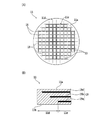
図1は、本実施形態で使用される被加工物(ワーク)11の構成例を模式的に示す斜視図である。図1に示すように、被加工物11は、例えば、シリコン(Si)、ヒ化ガリウム(GaAs)、リン化インジウム(InP)、窒化ガリウム(GaN)、シリコンカーバイド(SiC)等の半導体、サファイア(Al2O3)、ソーダガラス、ホウケイ酸ガラス、石英ガラス等の誘電体(絶縁体)、又は、タンタル酸リチウム(LiTa3)、ニオブ酸リチウム(LiNb3)等の強誘電体(強誘電体結晶)でなる円盤状のウェーハ(基板)である。
FIG. 1 is a perspective view schematically showing a configuration example of a work piece (work) 11 used in the present embodiment. As shown in FIG. 1, the
被加工物11の表面11a側は、交差する複数の分割予定ライン(ストリート)13でチップとなる複数の領域15に区画されている。なお、以下では、チップとなる複数の領域15の全てを含む概ね円形の領域をチップ領域11cと呼び、チップ領域11cを囲む環状の領域を外周余剰領域11dと呼ぶ。
The
チップ領域11c内の各領域15には、必要に応じて、IC(Integrated Circuit)、MEMS(Micro Electro Mechanical Systems)、LED(Light Emitting Diode)、LD(Laser Diode)、フォトダイオード(Photodiode)、SAW(Surface Acoustic Wave)フィルタ、BAW(Bulk Acoustic Wave)フィルタ等のデバイスが形成されている。
In each
この被加工物11を分割予定ライン13に沿って分割することで、複数のチップが得られる。具体的には、被加工物11がシリコンウェーハの場合には、例えば、メモリやセンサ等として機能するチップが得られる。被加工物11がヒ化ガリウム基板やリン化インジウム基板、窒化ガリウム基板の場合には、例えば、発光素子や受光素子等として機能するチップが得られる。
By dividing the
被加工物11がシリコンカーバイド基板の場合には、例えば、パワーデバイス等として機能するチップが得られる。被加工物11がサファイア基板の場合には、例えば、発光素子等として機能するチップが得られる。被加工物11がソーダガラスやホウケイ酸ガラス、石英ガラス等でなるガラス基板の場合には、例えば、光学部品やカバー部材(カバーガラス)として機能するチップが得られる。
When the
被加工物11がタンタル酸リチウムや、ニオブ酸リチウム等の強誘電体でなる強誘電体基板(強誘電体結晶基板)の場合には、例えば、フィルタやアクチュエータ等として機能するチップが得られる。なお、被加工物11の材質、形状、構造、大きさ、厚み等に制限はない。同様に、チップとなる領域15に形成されるデバイスの種類、数量、形状、構造、大きさ、配置等にも制限はない。チップとなる領域15には、デバイスが形成されていなくても良い。
When the
本実施形態に係るチップの製造方法では、被加工物11として円盤状のシリコンウェーハを用い、複数のチップを製造する。具体的には、まず、この被加工物11をチャックテーブルで直に保持する保持ステップを行う。図2は、本実施形態で使用されるレーザ加工装置の構成例を模式的に示す斜視図である。
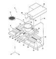
In the chip manufacturing method according to the present embodiment, a disk-shaped silicon wafer is used as the
図2に示すように、レーザ加工装置2は、各構成要素が搭載される基台4を備えている。基台4の上面には、被加工物11を吸引、保持するためのチャックテーブル(保持テーブル)6をX軸方向(加工送り方向)及びY軸方向(割り出し送り方向)に移動させる水平移動機構8が設けられている。水平移動機構8は、基台4の上面に固定されX軸方向に概ね平行な一対のX軸ガイドレール10を備えている。
As shown in FIG. 2, the
X軸ガイドレール10には、X軸移動テーブル12がスライド可能に取り付けられている。X軸移動テーブル12の裏面側(下面側)には、ナット部(不図示)が設けられており、このナット部には、X軸ガイドレール10に概ね平行なX軸ボールネジ14が螺合されている。
An X-axis moving table 12 is slidably attached to the
X軸ボールネジ14の一端部には、X軸パルスモータ16が連結されている。X軸パルスモータ16でX軸ボールネジ14を回転させることにより、X軸移動テーブル12はX軸ガイドレール10に沿ってX軸方向に移動する。X軸ガイドレール10に隣接する位置には、X軸方向においてX軸移動テーブル12の位置を検出するためのX軸スケール18が設置されている。
An
X軸移動テーブル12の表面(上面)には、Y軸方向に概ね平行な一対のY軸ガイドレール20が固定されている。Y軸ガイドレール20には、Y軸移動テーブル22がスライド可能に取り付けられている。Y軸移動テーブル22の裏面側(下面側)には、ナット部(不図示)が設けられており、このナット部には、Y軸ガイドレール20に概ね平行なY軸ボールネジ24が螺合されている。
A pair of Y-axis guide rails 20 substantially parallel to the Y-axis direction are fixed to the surface (upper surface) of the X-axis moving table 12. A Y-axis moving table 22 is slidably attached to the Y-
Y軸ボールネジ24の一端部には、Y軸パルスモータ26が連結されている。Y軸パルスモータ26でY軸ボールネジ24を回転させることにより、Y軸移動テーブル22はY軸ガイドレール20に沿ってY軸方向に移動する。Y軸ガイドレール20に隣接する位置には、Y軸方向においてY軸移動テーブル22の位置を検出するためのY軸スケール28が設置されている。
A Y-
Y軸移動テーブル22の表面側(上面側)には、支持台30が設けられており、この支持台30の上部には、チャックテーブル6が配置されている。チャックテーブル6の表面(上面)は、上述した被加工物11の裏面11b側(又は表面11a側)を吸引、保持する保持面6aになっている。保持面6aは、例えば、酸化アルミニウム等の硬度が高い多孔質材で構成されている。ただし、保持面6aは、ポリエチレンやエポキシ等の樹脂に代表される柔軟な材料で構成されていても良い。
A
この保持面6aは、チャックテーブル6の内部に形成された吸引路6b(図3(A)等参照)やバルブ32(図3(A)等参照)等を介して吸引源34(図3(A)等参照)に接続されている。チャックテーブル6の下方には、回転駆動源(不図示)が設けられており、チャックテーブル6は、この回転駆動源によってZ軸方向に概ね平行な回転軸の周りに回転する。
The holding
水平移動機構8の後方には、柱状の支持構造36が設けられている。支持構造36の上部には、Y軸方向に伸びる支持アーム38が固定されており、この支持アーム38の先端部には、被加工物11に対して透過性を有する波長(吸収され難い波長)のレーザビーム17(図3(B)参照)をパルス発振して、チャックテーブル6上の被加工物11に照射するレーザ照射ユニット40が設けられている。
A
レーザ照射ユニット40に隣接する位置には、被加工物11の表面11a側又は裏面11b側を撮像するカメラ42が設けられている。カメラ42で被加工物11等を撮像して形成された画像は、例えば、被加工物11とレーザ照射ユニット40との位置等を調整する際に使用される。
At a position adjacent to the
チャックテーブル6、水平移動機構8、レーザ照射ユニット40、カメラ42等の構成要素は、制御ユニット(不図示)に接続されている。制御ユニットは、被加工物11が適切に加工されるように各構成要素を制御する。
Components such as the chuck table 6, the horizontal movement mechanism 8, the
図3(A)は、保持ステップについて説明するための断面図である。なお、図3(A)では、一部の構成要素を機能ブロックで示している。保持ステップでは、図3(A)に示すように、例えば、被加工物11の裏面11bをチャックテーブル6の保持面6aに接触させる。そして、バルブ32を開いて吸引源34の負圧を保持面6aに作用させる。
FIG. 3A is a cross-sectional view for explaining the holding step. In addition, in FIG. 3A, some components are shown by functional blocks. In the holding step, as shown in FIG. 3A, for example, the
これにより、被加工物11は、表面11a側が上方に露出した状態でチャックテーブル6に吸引、保持される。なお、本実施形態では、図3(A)に示すように、被加工物11の裏面11b側をチャックテーブル6で直に保持する。つまり、本実施形態では、被加工物11に対してエキスパンドシートを貼る必要がない。
As a result, the
保持ステップの後には、被加工物11に対して透過性を有する波長のレーザビーム17を照射し、分割予定ライン13に沿う改質層を形成する第1レーザ加工ステップ及び第2レーザ加工ステップを行う。なお、本実施形態では、第1レーザ加工ステップの後に第2レーザ加工ステップを行う場合について説明する。
After the holding step, a first laser machining step and a second laser machining step are performed in which the
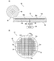
図3(B)は、第1レーザ加工ステップ及び第2レーザ加工ステップについて説明するための断面図であり、図4(A)は、全ての分割予定ライン13に沿って改質層が形成された後の被加工物11の状態を模式的に示す平面図であり、図4(B)は、各分割予定ライン13に沿って形成された改質層を模式的に示す断面図である。なお、図3(B)では、一部の構成要素を機能ブロックで示している。
FIG. 3B is a cross-sectional view for explaining the first laser machining step and the second laser machining step, and FIG. 4A shows a modified layer formed along all the planned division lines 13. FIG. 4B is a plan view schematically showing the state of the
第1レーザ加工ステップでは、まず、チャックテーブル6を回転させて、例えば、対象となる分割予定ライン13の延びる方向をX軸方向に対して平行にする。次に、チャックテーブル6を移動させて、対象となる分割予定ライン13の延長線上にレーザ照射ユニット40の位置を合わせる。そして、図3(B)に示すように、X軸方向(すなわち、対象の分割予定ライン13の延びる方向)にチャックテーブル6を移動させる。
In the first laser machining step, first, the chuck table 6 is rotated so that, for example, the extending direction of the target division scheduled
その後、対象となる分割予定ライン13上の2箇所に存在するチップ領域11cと外周余剰領域11dとの境界の一方の直上にレーザ照射ユニット40が到達したタイミングで、このレーザ照射ユニット40からレーザビーム17の照射を開始する。本実施形態では、図3(B)に示すように、被加工物11の上方に配置されたレーザ照射ユニット40から、被加工物11の表面11aに向けてレーザビーム17が照射される。
After that, when the
このレーザビーム17の照射は、レーザ照射ユニット40が、対象となる分割予定ライン13上の2箇所に存在するチップ領域11cと外周余剰領域11dとの境界の他方の直上に到達するまで続けられる。つまり、ここでは、対象の分割予定ライン13に沿ってチップ領域11c内にのみレーザビーム17を照射する。
The irradiation of the
また、このレーザビーム17は、被加工物11の内部の表面11a(又は裏面11b)から第1深さの位置に集光点を位置付けるように照射される。このように、被加工物11に対して透過性を有する波長のレーザビーム17を、被加工物11の内部に集光させることで、集光点及びその近傍で被加工物11の一部を多光子吸収により改質し、分割の起点となる改質層19(第1改質層19a)を形成できる(第1改質層形成ステップ)。
Further, the
本実施形態の第1レーザ加工ステップでは、対象の分割予定ライン13に沿ってチップ領域11c内にのみレーザビーム17を照射するので、対象の分割予定ライン13に沿ってチップ領域11c内にのみ改質層19(第1改質層19a)が形成される。すなわち、図4(B)に示すように、第1レーザ加工ステップでは、外周余剰領域11dに改質層19(第1改質層19a)が形成されない。
In the first laser machining step of the present embodiment, since the
上述した第1レーザ加工ステップの後には、同じ分割予定ライン13に沿って第1深さとは異なる深さの位置に改質層19を形成する第2レーザ加工ステップを行う。なお、第1レーザ加工ステップが終了した段階では、対象となる分割予定ライン13の延長線上にレーザ照射ユニット40が存在するので、このレーザ照射ユニット40の位置を分割予定ライン13に合わせて調整する必要はない。
After the first laser machining step described above, a second laser machining step is performed to form the modified
第2レーザ加工ステップでは、まず、チャックテーブル6をX軸方向(対象の分割予定ライン13の延びる方向)に移動させる。次に、被加工物11の外周余剰領域11dに設定された照射開始点の直上にレーザ照射ユニット40が到達したタイミングで、このレーザ照射ユニット40からレーザビーム17の照射を開始する。
In the second laser machining step, first, the chuck table 6 is moved in the X-axis direction (the direction in which the target division scheduled
本実施形態では、第1レーザ加工ステップと同様に、被加工物11の上方に配置されたレーザ照射ユニット40から、被加工物11の表面11aに向けてレーザビーム17が照射される。このレーザビーム17の照射は、レーザ照射ユニット40が、被加工物11のチップ領域11c上を通過して外周余剰領域11dに設定された照射終了点の直上に到達するまで続けられる。
In the present embodiment, similarly to the first laser machining step, the
つまり、ここでは、対象の分割予定ライン13に沿って外周余剰領域11dの一部及びチップ領域11cにレーザビーム17を照射する。また、このレーザビーム17は、被加工物11の内部の表面11a(又は裏面11b)から第2深さ(第1深さとは異なる深さ)の位置に集光点を位置付けるように照射される。
That is, here, the
これにより、第1レーザ加工ステップで形成される改質層19(第1改質層19a)より長く外周余剰領域11dに端部が重なる改質層19(第2改質層19b)を、分割予定ライン13に沿って第2深さの位置に形成できる(第2改質層形成ステップ)。第2深さの位置に改質層19(第2改質層19b)を形成した後には、同様の手順で第1深さ及び第2深さとは異なる第3深さの位置に改質層19(第3改質層19c)を形成する(第3改質層形成ステップ)。第3深さの位置に改質層19を形成する際には、照射開始点及び照射終了点の位置を変更して良い。
As a result, the modified layer 19 (second modified
なお、本実施形態では、第1レーザ加工ステップで1つの分割予定ライン13に沿って1つの改質層19(第1改質層19a)を形成し、第2レーザ加工ステップで同じ1つの分割予定ライン13に沿って2つの改質層19(第2改質層19b及び第3改質層19c)を形成しているが、1つの分割予定ライン13に沿って形成される改質層19の数や位置等に特段の制限はない。
In the present embodiment, one modified layer 19 (first modified layer 19a) is formed along one scheduled
例えば、第1レーザ加工ステップで1つの分割予定ライン13に沿って形成される改質層19の数は2つ以上でも良い。また、第2レーザ加工ステップで同じ1つの分割予定ライン13に沿って形成される改質層19の数は1つ、又は3つ以上でも良い。すなわち、少なくとも、第1レーザ加工ステップで1つの分割予定ライン13に沿って1つ以上の改質層19を形成でき、第2レーザ加工ステップで1つの分割予定ライン13に沿って1つ以上の改質層19を形成できれば良い。
For example, the number of modified
また、改質層19は、表面11a(又は裏面11b)にクラックが到達する条件で形成されることが望ましい。もちろん、表面11a及び裏面11bの両方にクラックが到達する条件で改質層19を形成しても良い。これにより、被加工物11をより適切に分割できるようになる。
Further, it is desirable that the modified
被加工物11がシリコンウェーハの場合には、例えば、次のような条件で改質層19が形成される。
被加工物:シリコンウェーハ
レーザビームの波長:1340nm
レーザビームの繰り返し周波数:90kHz
レーザビームの出力:0.1W〜2W
チャックテーブルの移動速度(加工送り速度):180mm/s〜1000mm/s、代表的には、500mm/s
When the
Work piece: Silicon wafer Laser beam wavelength: 1340 nm
Laser beam repetition frequency: 90 kHz
Laser beam output: 0.1W to 2W
Chuck table moving speed (machining feed rate): 180 mm / s to 1000 mm / s, typically 500 mm / s
被加工物11がヒ化ガリウム基板やリン化インジウム基板の場合には、例えば、次のような条件で改質層19が形成される。
被加工物:ヒ化ガリウム基板、リン化インジウム基板
レーザビームの波長:1064nm
レーザビームの繰り返し周波数:20kHz
レーザビームの出力:0.1W〜2W
チャックテーブルの移動速度(加工送り速度):100mm/s〜400mm/s、代表的には、200mm/s
When the
Work piece: Gallium arsenide substrate, Indium phosphide substrate Laser beam wavelength: 1064 nm
Laser beam repetition frequency: 20 kHz
Laser beam output: 0.1W to 2W
Chuck table moving speed (machining feed rate): 100 mm / s to 400 mm / s, typically 200 mm / s
被加工物11がサファイア基板の場合には、例えば、次のような条件で改質層19が形成される。
被加工物:サファイア基板
レーザビームの波長:1045nm
レーザビームの繰り返し周波数:100kHz
レーザビームの出力:0.1W〜2W
チャックテーブルの移動速度(加工送り速度):400mm/s〜800mm/s、代表的には、500mm/s
When the
Work piece: Sapphire substrate Laser beam wavelength: 1045 nm
Laser beam repetition frequency: 100 kHz
Laser beam output: 0.1W to 2W
Chuck table moving speed (machining feed rate): 400 mm / s to 800 mm / s, typically 500 mm / s
被加工物11がタンタル酸リチウムやニオブ酸リチウム等の強誘電体でなる強誘電体基板の場合には、例えば、次のような条件で改質層19が形成される。
被加工物:タンタル酸リチウム基板、ニオブ酸リチウム基板
レーザビームの波長:532nm
レーザビームの繰り返し周波数:15kHz
レーザビームの出力:0.02W〜0.2W
チャックテーブルの移動速度(加工送り速度):270mm/s〜420mm/s、代表的には、300mm/s
When the
Work piece: Lithium tantalate substrate, Lithium niobate substrate Laser beam wavelength: 532 nm
Laser beam repetition frequency: 15 kHz
Laser beam output: 0.02W to 0.2W
Chuck table moving speed (machining feed rate): 270 mm / s to 420 mm / s, typically 300 mm / s
被加工物11がソーダガラスやホウケイ酸ガラス、石英ガラス等でなるガラス基板の場合には、例えば、次のような条件で改質層19が形成される。
被加工物:ソーダガラス基板、ホウケイ酸ガラス基板、石英ガラス基板
レーザビームの波長:532nm
レーザビームの繰り返し周波数:50kHz
レーザビームの出力:0.1W〜2W
チャックテーブルの移動速度(加工送り速度):300mm/s〜600mm/s、代表的には、400mm/s
When the
Workpiece: Soda glass substrate, borosilicate glass substrate, quartz glass substrate Laser beam wavelength: 532 nm
Laser beam repetition frequency: 50 kHz
Laser beam output: 0.1W to 2W
Chuck table moving speed (machining feed rate): 300 mm / s to 600 mm / s, typically 400 mm / s
被加工物11が窒化ガリウム基板の場合には、例えば、次のような条件で改質層19が形成される。
被加工物:窒化ガリウム基板
レーザビームの波長:532nm
レーザビームの繰り返し周波数:25kHz
レーザビームの出力:0.02W〜0.2W
チャックテーブルの移動速度(加工送り速度):90mm/s〜600mm/s、代表的には、150mm/s
When the
Work piece: Gallium nitride substrate Laser beam wavelength: 532 nm
Laser beam repetition frequency: 25 kHz
Laser beam output: 0.02W to 0.2W
Chuck table moving speed (machining feed rate): 90 mm / s to 600 mm / s, typically 150 mm / s
被加工物11がシリコンカーバイド基板の場合には、例えば、次のような条件で改質層19が形成される。
被加工物:シリコンカーバイド基板
レーザビームの波長:532nm
レーザビームの繰り返し周波数:25kHz
レーザビームの出力:0.02W〜0.2W、代表的には、0.1W
チャックテーブルの移動速度(加工送り速度):90mm/s〜600mm/s、代表的には、シリコンカーバイド基板の劈開方向で90mm/s、非劈開方向で400mm/s
When the
Work piece: Silicon carbide substrate Laser beam wavelength: 532 nm
Laser beam repetition frequency: 25 kHz
Laser beam output: 0.02W to 0.2W, typically 0.1W
Chuck table moving speed (machining feed rate): 90 mm / s to 600 mm / s, typically 90 mm / s in the cleavage direction of the silicon carbide substrate, 400 mm / s in the non-cleavage direction.
対象の分割予定ライン13に沿って改質層19を形成した後には、残りの全ての分割予定ライン13に対して上述した第1レーザ加工ステップ及び第2レーザ加工ステップを繰り返す。これにより、図4(A)に示すように、全ての分割予定ライン13に沿って改質層19を形成できる。
After forming the modified
本実施形態の第1レーザ加工ステップでは、分割予定ライン13に沿ってチップ領域11c内にのみ改質層19(第1改質層19a)を形成し、外周余剰領域11dには改質層19(第1改質層19a)を形成しないので、この外周余剰領域11dによって被加工物11の強度が保たれる。これにより、搬送等の際に加わる力によって被加工物11が個々のチップへと分割されてしまうことはない。このように、第1レーザ加工ステップの後の外周余剰領域11dは、チップ領域11を補強するための補強部として機能する。
In the first laser machining step of the present embodiment, the modified layer 19 (first modified layer 19a) is formed only in the
また、本実施形態の第1レーザ加工ステップでは、外周余剰領域11dに改質層19(第1改質層19a)を形成しないので、例えば、改質層19から伸長するクラックが表面11a及び裏面11bの両方に到達し、被加工物11が完全に分割された状況でも、各チップが脱落、離散することはない。一般に、被加工物11に改質層19が形成されると、この改質層19の近傍で被加工物11は膨張する。本実施形態では、改質層19の形成によって発生する膨張の力を、補強部として機能するリング状の外周余剰領域11dで内向きに作用させることで、各チップを押さえつけ、脱落、離散を防止している。
Further, in the first laser machining step of the present embodiment, the modified layer 19 (first modified layer 19a) is not formed in the outer
第1レーザ加工ステップ及び第2レーザ加工ステップの後には、チャックテーブル6から被加工物11を搬出する搬出ステップを行う。具体的には、例えば、被加工物11の表面11a(又は、裏面11b)の全体を吸着、保持できる搬送ユニット(不図示)で被加工物11の表面11aの全体を吸着してから、バルブ32を閉じて吸引源34の負圧を遮断し、被加工物11を搬出する。なお、本実施形態では、上述のように、外周余剰領域11dが補強部として機能するので、搬送等の際に加わる力によって被加工物11が個々のチップへと分割されてしまい、被加工物11を適切に搬送できなくなることはない。
After the first laser machining step and the second laser machining step, a carry-out step of carrying out the workpiece 11 from the chuck table 6 is performed. Specifically, for example, a transfer unit (not shown) capable of sucking and holding the entire
搬出ステップの後には、被加工物11から補強部を除去する補強部除去ステップを行う。図5(A)及び図5(B)は、補強部除去ステップについて説明するための断面図である。なお、図5(A)及び図5(B)では、一部の構成要素を機能ブロックで示している。補強部除去ステップは、例えば、図5(A)及び図5(B)に示す分割装置52を用いて行われる。
After the carry-out step, a reinforcing portion removing step of removing the reinforcing portion from the
分割装置52は、被加工物11を吸引、保持するためのチャックテーブル(保持テーブル)54を備えている。このチャックテーブル54の上面の一部は、被加工物11のチップ領域11cを吸引、保持する保持面54aになっている。保持面54aは、チャックテーブル54の内部に形成された吸引路54bやバルブ56等を介して吸引源58に接続されている。また、この保持面54aの下方には、ヒータ(加熱ユニット)54cが配置されている。
The dividing
チャックテーブル54の上面の別の一部には、被加工物11の外周余剰領域11d(すなわち、補強部)を吸引、保持するための吸引路54dの一端が開口している。吸引路54dの他端側は、バルブ60等を介して吸引源58に接続されている。このチャックテーブル54は、モータ等の回転駆動源(不図示)に連結されており、鉛直方向に概ね平行な回転軸の周りに回転する。
One end of a
チャックテーブル54の上方には、切削ユニット62が配置されている。切削ユニット62は、保持面54aに対して概ね平行な回転軸となるスピンドル64を備えている。スピンドル64の一端側には、結合材に砥粒が分散されてなる環状の切削ブレード66が装着されている。
A cutting
スピンドル64の他端側には、モータ等の回転駆動源(不図示)が連結されており、スピンドル64の一端側に装着された切削ブレード66は、この回転駆動源から伝わる力によって回転する。切削ユニット62は、例えば、昇降機構(不図示)に支持されており、切削ブレード66は、この昇降機構によって鉛直方向に移動する。
A rotary drive source (not shown) such as a motor is connected to the other end side of the
なお、チャックテーブル54の上面には、被加工物11のチップ領域11cと外周余剰領域11dとの境界に対応する位置に、切削ブレード66との接触を防ぐための切削ブレード用逃げ溝(不図示)が形成されている。
A relief groove for a cutting blade (not shown) is provided on the upper surface of the chuck table 54 at a position corresponding to the boundary between the
補強部除去ステップでは、まず、被加工物11の裏面11bをチャックテーブル54の保持面54aに接触させる。そして、バルブ56,60を開き、吸引源58の負圧を保持面54a等に作用させる。これにより、被加工物11は、表面11a側が上方に露出した状態でチャックテーブル54に吸引、保持される。なお、本実施形態では、図5(A)に示すように、被加工物11の裏面11b側をチャックテーブル54で直に保持する。つまり、ここでも、被加工物11に対してエキスパンドシートを貼る必要がない。
In the reinforcing portion removing step, first, the
次に、切削ブレード66を回転させて、被加工物11のチップ領域11cと外周余剰領域11dとの境界に切り込ませる。併せて、図5(A)に示すように、チャックテーブル54を、鉛直方向に概ね平行な回転軸の周りに回転させる。これにより、チップ領域11cと外周余剰領域11dとの境界に沿って被加工物11を切断できる。
Next, the
その後、バルブ60を閉じて、被加工物11の外周余剰領域11dに対する吸引源58の負圧を遮断する。そして、図5(B)に示すように、チャックテーブル54から外周余剰領域11dを除去する。これにより、チャックテーブル54上には、被加工物11のチップ領域11cのみが残る。
After that, the
補強部除去ステップの後には、被加工物11を個々のチップへと分割する分割ステップを行う。具体的には、加熱及び冷却により応力を生じさせて被加工物11を分割する。図6は、分割ステップについて説明するための断面図である。なお、図6では、一部の構成要素を機能ブロックで示している。
After the reinforcing portion removing step, a division step of dividing the
分割ステップは、引き続き分割装置52を用いて行われる。図6に示すように、分割装置52は、チャックテーブル54の上方に配置されたノズル(冷却ユニット)68を更に備えている。本実施形態の分割ステップでは、チャックテーブル54に設けられたヒータ54cで被加工物11を加熱した後に、このノズル68から冷却用の流体21を供給して被加工物11を冷却することで、被加工物11の分割に必要な応力を生じさせる。
The division step is subsequently performed using the
冷却用の流体21としては、例えば、水等の液体や、エア等の気体を用いることができる。流体21として液体を用いる場合には、この液体を凍結しない程度に低い温度(例えば、凝固点より0.1℃〜10℃ほど高い温度)まで冷却しておいても良い。ただし、流体21の種類や流量、温度等に特段の制限はない。例えば、気化することによって更に熱を奪うことのできる液体窒素等の低温の液体を用いても良い。
As the cooling
ヒータ54cを作動させて被加工物11を加熱した後に、ノズル68から冷却用の流体21を供給して被加工物11を冷却すると、被加工物11の内部に発生する応力によって改質層19からクラック23が伸長する。これにより、被加工物11は分割予定ライン13に沿って複数のチップ25へと分割される。
After the
加熱及び冷却の条件(温度、時間等)は、被加工物11の種類等に応じて設定される。また、ヒータ54cによる被加工物11の加熱と、ノズル68から供給される液体21による被加工物11の冷却とは、被加工物11が適切に分割されるまで繰り返されることが望ましい。
The heating and cooling conditions (temperature, time, etc.) are set according to the type of the
このように、本実施形態では、加熱及び冷却によって必要な力を付与することで、被加工物11を個々のチップ25へと分割できる。なお、本実施形態では、被加工物11を加熱した後に冷却しているが、被加工物11を冷却した後に加熱しても良い。加熱及び冷却の方法にも、特段の制限はない。
As described above, in the present embodiment, the
以上のように、本実施形態に係るチップの製造方法では、被加工物(ワーク)11をチャックテーブル(保持テーブル)6で直に保持した状態で、集光点を第1深さの位置に位置付けるように被加工物11のチップ領域11cにのみレーザビーム17を照射して、チップ領域11cの分割予定ライン13に沿って改質層19(第1改質層19a)を形成し、また、集光点を第2深さの位置及び第3深さの位置に位置づけるようにレーザビーム17を照射して、第1深さの位置に形成される改質層19より長く外周余剰領域11dに端部が重なる改質層19(第2改質層19b及び第3改質層19c)を分割予定ライン13に沿って形成した後、加熱と冷却とにより力を付与して被加工物11を個々のチップ25へと分割するので、被加工物11に力を加えて個々のチップ25へと分割するためにエキスパンドシートを用いる必要がない。このように、本実施形態に係るチップの製造方法によれば、エキスパンドシートを用いることなく板状の被加工物11であるシリコンウェーハを分割して複数のチップ25を製造できる。
As described above, in the chip manufacturing method according to the present embodiment, the light collecting point is set to the position of the first depth while the workpiece (work) 11 is directly held by the chuck table (holding table) 6. The
また、本実施形態に係るチップの製造方法では、被加工物11のチップ領域11cにのみレーザビーム17を照射して分割予定ライン13に沿う改質層19(第1改質層19a)を形成するとともに、外周余剰領域11dを改質層19が形成されていない補強部とするので、この補強部によってチップ領域11cは補強される。よって、搬送等の際に加わる力によって被加工物11が個々のチップ25へと分割されてしまい、被加工物11を適切に搬送できなくなることもない。
Further, in the chip manufacturing method according to the present embodiment, the
なお、本発明は、上記実施形態等の記載に制限されず種々変更して実施可能である。例えば、上記実施形態では、第1レーザ加工ステップの後に第2レーザ加工ステップを行っているが、第2レーザ加工ステップの後に第1レーザ加工ステップを行うようにしても良い。更に、第2改質層19bを形成する第2改質層形成ステップと、第3改質層19cを形成する第3改質層形成ステップとの順序を入れ替えても良い。
The present invention is not limited to the description of the above embodiment and can be implemented with various modifications. For example, in the above embodiment, the second laser machining step is performed after the first laser machining step, but the first laser machining step may be performed after the second laser machining step. Further, the order of the second modified layer forming step for forming the second modified
また、上記実施形態では、対象の1本の分割予定ライン13に対して第1レーザ加工ステップを行った後に、同じ1本の分割予定ライン13に対して第2レーザ加工ステップを行っているが、本発明は、この態様に制限されない。例えば、複数の分割予定ライン13に対して第1改質層19aを形成する第1レーザ加工ステップ(第1改質層形成ステップ)を行った後に、複数の分割予定ライン13に対して第2レーザ加工ステップを行うこともできる。
Further, in the above embodiment, after the first laser machining step is performed on the target one scheduled
なお、この場合には、複数の分割予定ライン13に対して第2改質層19bを形成する第2レーザ加工ステップ(第2改質層形成ステップ)を行ってから、複数の分割予定ライン13に対して第3改質層19cを形成する第2レーザ加工ステップ(第3改質層形成ステップ)を行うと良い。
In this case, after performing the second laser machining step (second modified layer forming step) for forming the second modified
より具体的には、例えば、まず、第1方向に平行な全ての分割予定ライン13に対して第1改質層19aを形成する第1改質層形成ステップを行う。次に、第1方向に平行な全ての分割予定ライン13に対して第2改質層19bを形成する第2改質層形成ステップを行う。そして、第1方向に平行な全ての分割予定ライン13に対して第3改質層19cを形成する第3改質層形成ステップを行う。
More specifically, for example, first, a first modified layer forming step of forming the first modified layer 19a on all scheduled division lines 13 parallel to the first direction is performed. Next, a second modified layer forming step is performed in which the second modified
その後、第1方向とは異なる第2方向に平行な全ての分割予定ライン13に対して第1改質層19aを形成する第1改質層形成ステップを行う。次に、第2方向に平行な全ての分割予定ライン13に対して第2改質層19bを形成する第2改質層形成ステップを行う。そして、第2方向に平行な全ての分割予定ライン13に対して第3改質層19cを形成する第3改質層形成ステップを行う。
After that, a first modified layer forming step of forming the first modified layer 19a is performed on all scheduled division lines 13 parallel to the second direction different from the first direction. Next, a second modified layer forming step is performed to form the second modified
なお、この場合にも、第2レーザ加工ステップ(第2改質層形成ステップ及び第3改質層形成ステップ)の後に第1レーザ加工ステップ(第1改質層形成ステップ)を行うことができる。同様に、第2改質層19bを形成する第2改質層形成ステップと、第3改質層19cを形成する第3改質層形成ステップとの順序を入れ替えても良い。
Also in this case, the first laser machining step (first modified layer forming step) can be performed after the second laser machining step (second modified layer forming step and third modified layer forming step). .. Similarly, the order of the second modified layer forming step for forming the second modified
また、上記実施形態では、被加工物11の裏面11b側をチャックテーブル6で直に保持して、表面11a側からレーザビーム17を照射しているが、被加工物11の表面11a側をチャックテーブル6で直に保持して、裏面11b側からレーザビーム17を照射しても良い。
Further, in the above embodiment, the
図7は、変形例に係る保持ステップについて説明するための断面図である。この変形例に係る保持ステップでは、図7に示すように、例えば、ポリエチレンやエポキシ等の樹脂に代表される柔軟な材料でなる多孔質状のシート(ポーラスシート)44によって上面が構成されたチャックテーブル(保持テーブル)6を用いると良い。 FIG. 7 is a cross-sectional view for explaining the holding step according to the modified example. In the holding step according to this modification, as shown in FIG. 7, a chuck whose upper surface is formed of, for example, a porous sheet (porous sheet) 44 made of a flexible material typified by a resin such as polyethylene or epoxy. It is preferable to use the table (holding table) 6.
このチャックテーブル6では、シート44の上面44aで被加工物11の表面11a側を吸引、保持することになる。これにより、表面11a側に形成されているデバイス等の破損を防止できる。このシート44はチャックテーブル6の一部であり、チャックテーブル6の本体等とともに繰り返し使用される。
In the chuck table 6, the
ただし、チャックテーブル6の上面は、上述した多孔質状のシート44によって構成されている必要はなく、少なくとも、被加工物11の表面11a側に形成されているデバイス等を傷つけない程度に柔軟な材料で構成されていれば良い。また、シート44は、チャックテーブル6の本体に対して着脱できるように構成され、破損した場合等に交換できることが望ましい。
However, the upper surface of the chuck table 6 does not have to be formed of the above-mentioned
また、上記実施形態では、搬出ステップの後、分割ステップの前に、補強部除去ステップを行っているが、例えば、第1レーザ加工ステップ及び第2レーザ加工ステップの後、搬出ステップの前に、補強部除去ステップを行っても良い。なお、搬出ステップの後、分割ステップの前に、補強部除去ステップを行う場合には、補強部除去ステップの後に被加工物11を搬送する必要がないので、被加工物11を適切に搬送できなくなる等の不具合を回避し易い。
Further, in the above embodiment, the reinforcing portion removing step is performed after the carry-out step and before the division step. For example, after the first laser machining step and the second laser machining step and before the carry-out step, The reinforcing portion removing step may be performed. When the reinforcing portion removing step is performed after the carry-out step and before the dividing step, it is not necessary to transport the
また、補強部除去ステップを省略することもできる。上記実施形態の第2レーザ加工ステップでは、外周余剰領域11dに端部が重なる改質層19(第2改質層19b及び第3改質層19c)を、分割予定ライン13に沿って形成している。そのため、改質層19と外周余剰領域11dとが重ならない場合に比べて、外周余剰領域11dは分割され易い。よって、補強部除去ステップを行わなくとも、分割ステップでチップ領域11cを外周余剰領域11dとともに分割することが可能になる。
Further, the step of removing the reinforcing portion can be omitted. In the second laser machining step of the above embodiment, the modified layer 19 (second modified
なお、この場合には、例えば、被加工物11の外周縁から改質層19の端までの距離が2mm〜3mm程度になるように、第2レーザ加工ステップで改質層19を形成する範囲を調整すると良い。また、例えば、分割ステップでチップ領域11cを分割する前に、補強部に分割の起点となる溝を形成しても良い。図8(A)は、変形例に係る分割ステップについて説明するための断面図であり、図8(B)は、変形例に係る分割ステップの後の被加工物11の状態を模式的に示す平面図である。
In this case, for example, the range in which the modified
変形例に係る分割ステップでは、図8(A)及び図8(B)に示すように、外周余剰領域11d(すなわち、補強部)に切削ブレード66を切り込ませて、分割の起点となる溝11eを形成する。この溝11eは、例えば、分割予定ライン13に沿って形成されることが望ましい。このような溝11eを形成することで、熱衝撃によって被加工物11を外周余剰領域11dごと分割できるようになる。なお、変形例に係る分割ステップでは、チャックテーブル54の吸引路54dやバルブ60等を省略できる。
In the division step according to the modification, as shown in FIGS. 8A and 8B, the
その他、上記実施形態及び変形例に係る構造、方法等は、本発明の目的の範囲を逸脱しない限りにおいて適宜変更して実施できる。 In addition, the structures, methods, etc. according to the above-described embodiments and modifications can be appropriately modified and implemented as long as they do not deviate from the scope of the object of the present invention.
11 被加工物(ワーク)
11a 表面
11b 裏面
11c チップ領域
11d 外周余剰領域
13 分割予定ライン(ストリート)
15 領域
17 レーザビーム
19 改質層
19a 第1改質層
19b 第2改質層
19c 第3改質層
21 流体
23 クラック
25 チップ
2 レーザ加工装置
4 基台
6 チャックテーブル(保持テーブル)
6a 保持面
6b 吸引路
8 水平移動機構
10 X軸ガイドレール
12 X軸移動テーブル
14 X軸ボールネジ
16 X軸パルスモータ
18 X軸スケール
20 Y軸ガイドレール
22 Y軸移動テーブル
24 Y軸ボールネジ
26 Y軸パルスモータ
28 Y軸スケール
30 支持台
32 バルブ
34 吸引源
36 支持構造
38 支持アーム
40 レーザ照射ユニット
42 カメラ
44 シート(ポーラスシート)
44a 上面
52 分割装置
54 チャックテーブル(保持テーブル)
54a 保持面
54b 吸引路
54c ヒータ(加熱ユニット)
54d 吸引路
56 バルブ
58 吸引源
60 バルブ
62 切削ユニット
64 スピンドル
66 切削ブレード
68 ノズル(冷却ユニット)
11 Work piece (work)
15
Claims (3)
被加工物を保持テーブルで直に保持する保持ステップと、
該保持ステップを実施した後に、被加工物に対して透過性を有する波長のレーザビームの集光点を該保持テーブルに保持された被加工物の内部の第1深さの位置に位置づけるように該分割予定ラインに沿って被加工物の該チップ領域にのみ該レーザビームを照射し、該チップ領域の該分割予定ラインに沿って第1改質層を形成するとともに、該外周余剰領域を該第1改質層が形成されていない補強部とする第1レーザ加工ステップと、
該保持ステップを実施した後に、被加工物に対して透過性を有する波長のレーザビームの集光点を該保持テーブルに保持された被加工物の内部の該第1深さとは異なる第2深さの位置に位置づけるように該分割予定ラインに沿って該レーザビームを照射し、該第1改質層より長く該外周余剰領域に端部が重なる第2改質層を該分割予定ラインに沿って形成する第2レーザ加工ステップと、
該第1レーザ加工ステップ及び該第2レーザ加工ステップを実施した後に、該保持テーブルから被加工物を搬出する搬出ステップと、
該搬出ステップを実施した後に、被加工物に力を付与して被加工物を個々の該チップへと分割する分割ステップと、を備え、
該分割ステップでは、加熱と冷却とにより該力を付与して被加工物を個々の該チップへと分割することを特徴とするチップの製造方法。 A chip for producing a plurality of chips from a plate-shaped workpiece having a chip region divided into a plurality of regions to be chips by a plurality of intersecting scheduled division lines and an outer peripheral surplus region surrounding the chip region. It ’s a manufacturing method,
A holding step that holds the work piece directly on the holding table,
After performing the holding step, to position the position of the first depth of the interior of the workpiece the focal point of the laser beam having a wavelength which is held on the holding table with a passing through the workpiece The laser beam is irradiated only to the chip region of the work piece along the planned division line to form a first modified layer along the planned division line of the chip region, and the outer peripheral surplus region is formed. The first laser machining step of forming a reinforcing portion in which the first modified layer is not formed, and
After performing the holding step, the second depth different from the first depth of the interior of the workpiece the focal point of the laser beam having a wavelength which is held on the holding table with a passing through the workpiece The laser beam is irradiated along the planned division line so as to be positioned at the upper position, and the second modified layer whose end overlaps the outer peripheral surplus region, which is longer than the first modified layer, is along the planned division line. The second laser machining step to be formed
After performing the first laser machining step and the second laser machining step, a unloading step of unloading the workpiece from the holding table and a unloading step.
After performing the該搬out step, and a dividing step of dividing the a by applying a force workpiece into individual said chips to the workpiece,
In the dividing step, a method for producing a chip is characterized in that the force is applied by heating and cooling to divide the workpiece into individual chips.
該保持ステップでは、該柔軟な材料で被加工物の表面側を保持することを特徴とする請求項1又は請求項2に記載のチップの製造方法。 The upper surface of the holding table is made of a flexible material.
The method for producing a chip according to claim 1 or 2, wherein in the holding step, the surface side of the workpiece is held by the flexible material.
Priority Applications (4)
| Application Number | Priority Date | Filing Date | Title |
|---|---|---|---|
| JP2017182986A JP6896344B2 (en) | 2017-09-22 | 2017-09-22 | Chip manufacturing method |
| KR1020180106688A KR102578958B1 (en) | 2017-09-22 | 2018-09-06 | Method of manufacturing chip |
| CN201811080404.0A CN109531838B (en) | 2017-09-22 | 2018-09-17 | Method for manufacturing chip |
| TW107133067A TWI770280B (en) | 2017-09-22 | 2018-09-19 | Wafer manufacturing method |
Applications Claiming Priority (1)
| Application Number | Priority Date | Filing Date | Title |
|---|---|---|---|
| JP2017182986A JP6896344B2 (en) | 2017-09-22 | 2017-09-22 | Chip manufacturing method |
Publications (3)
| Publication Number | Publication Date |
|---|---|
| JP2019061980A JP2019061980A (en) | 2019-04-18 |
| JP2019061980A5 JP2019061980A5 (en) | 2020-03-05 |
| JP6896344B2 true JP6896344B2 (en) | 2021-06-30 |
Family
ID=65838977
Family Applications (1)
| Application Number | Title | Priority Date | Filing Date |
|---|---|---|---|
| JP2017182986A Active JP6896344B2 (en) | 2017-09-22 | 2017-09-22 | Chip manufacturing method |
Country Status (4)
| Country | Link |
|---|---|
| JP (1) | JP6896344B2 (en) |
| KR (1) | KR102578958B1 (en) |
| CN (1) | CN109531838B (en) |
| TW (1) | TWI770280B (en) |
Families Citing this family (1)
| Publication number | Priority date | Publication date | Assignee | Title |
|---|---|---|---|---|
| TWI733604B (en) * | 2020-06-10 | 2021-07-11 | 財團法人工業技術研究院 | Laser processing system and method for glass workpiece |
Family Cites Families (35)
| Publication number | Priority date | Publication date | Assignee | Title |
|---|---|---|---|---|
| JPS5939769B2 (en) * | 1981-03-27 | 1984-09-26 | 昭和情報機器株式会社 | input device |
| JP4659300B2 (en) * | 2000-09-13 | 2011-03-30 | 浜松ホトニクス株式会社 | Laser processing method and semiconductor chip manufacturing method |
| JP3408805B2 (en) | 2000-09-13 | 2003-05-19 | 浜松ホトニクス株式会社 | Cutting origin region forming method and workpiece cutting method |
| JP3842769B2 (en) * | 2003-09-01 | 2006-11-08 | 株式会社東芝 | Laser processing apparatus, laser processing method, and semiconductor device manufacturing method |
| US20060030156A1 (en) * | 2004-08-05 | 2006-02-09 | Applied Materials, Inc. | Abrasive conductive polishing article for electrochemical mechanical polishing |
| CN100481337C (en) * | 2004-12-08 | 2009-04-22 | 雷射先进科技株式会社 | Division starting point forming method in body to be divided, and dividing method for body to be divided |
| JP4198123B2 (en) * | 2005-03-22 | 2008-12-17 | 浜松ホトニクス株式会社 | Laser processing method |
| JP2007019379A (en) * | 2005-07-11 | 2007-01-25 | Disco Abrasive Syst Ltd | Method for processing wafer |
| CN100536108C (en) * | 2005-11-16 | 2009-09-02 | 株式会社电装 | Semiconductor device and dicing method for semiconductor substrate |
| US8728916B2 (en) * | 2009-02-25 | 2014-05-20 | Nichia Corporation | Method for manufacturing semiconductor element |
| JP5791866B2 (en) | 2009-03-06 | 2015-10-07 | 株式会社ディスコ | Work dividing device |
| JP2011061043A (en) * | 2009-09-10 | 2011-03-24 | Disco Abrasive Syst Ltd | Processing method, and method for manufacturing semiconductor device |
| JP5686551B2 (en) * | 2010-08-31 | 2015-03-18 | 株式会社ディスコ | Wafer processing method |
| JP5480169B2 (en) * | 2011-01-13 | 2014-04-23 | 浜松ホトニクス株式会社 | Laser processing method |
| TWI457191B (en) * | 2011-02-04 | 2014-10-21 | Mitsuboshi Diamond Ind Co Ltd | Laser scribing method and laser processing apparatus |
| KR20130033114A (en) * | 2011-09-26 | 2013-04-03 | 주식회사 이오테크닉스 | Laser processing method |
| JP5939769B2 (en) | 2011-11-11 | 2016-06-22 | 株式会社ディスコ | Processing method of plate |
| JP5964580B2 (en) * | 2011-12-26 | 2016-08-03 | 株式会社ディスコ | Wafer processing method |
| JP2013152987A (en) * | 2012-01-24 | 2013-08-08 | Disco Abrasive Syst Ltd | Method for processing wafer |
| JP2013236001A (en) * | 2012-05-10 | 2013-11-21 | Disco Abrasive Syst Ltd | Method for dividing plate-like object |
| JP2014199834A (en) * | 2013-03-29 | 2014-10-23 | 株式会社ディスコ | Holding means and processing method |
| JP2014236034A (en) * | 2013-05-31 | 2014-12-15 | 株式会社ディスコ | Method for processing wafer |
| US9236284B2 (en) * | 2014-01-31 | 2016-01-12 | Applied Materials, Inc. | Cooled tape frame lift and low contact shadow ring for plasma heat isolation |
| CN105171235B (en) * | 2014-06-23 | 2018-06-01 | 大族激光科技产业集团股份有限公司 | A kind of double focus laser micromachining device and its processing method |
| JP6399914B2 (en) * | 2014-12-04 | 2018-10-03 | 株式会社ディスコ | Wafer generation method |
| JP6395613B2 (en) * | 2015-01-06 | 2018-09-26 | 株式会社ディスコ | Wafer generation method |
| JP6456228B2 (en) * | 2015-04-15 | 2019-01-23 | 株式会社ディスコ | Thin plate separation method |
| JP6482389B2 (en) * | 2015-06-02 | 2019-03-13 | 株式会社ディスコ | Wafer generation method |
| JP6472347B2 (en) * | 2015-07-21 | 2019-02-20 | 株式会社ディスコ | Thinning method of wafer |
| WO2017025550A1 (en) * | 2015-08-10 | 2017-02-16 | Saint-Gobain Glass France | Method for cutting a thin glass layer |
| JP6486239B2 (en) * | 2015-08-18 | 2019-03-20 | 株式会社ディスコ | Wafer processing method |
| JP6504977B2 (en) * | 2015-09-16 | 2019-04-24 | 株式会社ディスコ | Wafer processing method |
| JP6605278B2 (en) * | 2015-09-29 | 2019-11-13 | 浜松ホトニクス株式会社 | Laser processing method |
| JP2017107903A (en) * | 2015-12-07 | 2017-06-15 | 株式会社ディスコ | Processing method of wafer |
| CN106328778B (en) * | 2016-09-14 | 2019-03-08 | 中国科学院半导体研究所 | Stealth cutting preparation just, fall and inverted trapezoidal mesa-shaped substrate LED chip method |
-
2017
- 2017-09-22 JP JP2017182986A patent/JP6896344B2/en active Active
-
2018
- 2018-09-06 KR KR1020180106688A patent/KR102578958B1/en active IP Right Grant
- 2018-09-17 CN CN201811080404.0A patent/CN109531838B/en active Active
- 2018-09-19 TW TW107133067A patent/TWI770280B/en active
Also Published As
| Publication number | Publication date |
|---|---|
| CN109531838A (en) | 2019-03-29 |
| TW201916138A (en) | 2019-04-16 |
| KR20190034085A (en) | 2019-04-01 |
| JP2019061980A (en) | 2019-04-18 |
| TWI770280B (en) | 2022-07-11 |
| CN109531838B (en) | 2021-12-21 |
| KR102578958B1 (en) | 2023-09-14 |
Similar Documents
| Publication | Publication Date | Title |
|---|---|---|
| JP6896344B2 (en) | Chip manufacturing method | |
| JP7058905B2 (en) | How to make chips | |
| JP7031963B2 (en) | How to make chips | |
| JP6925720B2 (en) | Chip manufacturing method | |
| JP6925721B2 (en) | Chip manufacturing method | |
| JP6855127B2 (en) | Chip manufacturing method | |
| JP6851690B2 (en) | Chip manufacturing method | |
| JP6925717B2 (en) | Chip manufacturing method | |
| JP6918424B2 (en) | Chip manufacturing method | |
| JP6918423B2 (en) | Chip manufacturing method | |
| JP6903378B2 (en) | Chip manufacturing method | |
| JP6918422B2 (en) | Chip manufacturing method | |
| JP6903379B2 (en) | Chip manufacturing method | |
| JP6830739B2 (en) | How to make chips | |
| JP7031966B2 (en) | How to make chips | |
| JP7031965B2 (en) | How to make chips | |
| JP7031964B2 (en) | How to make chips | |
| JP6851691B2 (en) | Chip manufacturing method | |
| JP6925722B2 (en) | Chip manufacturing method | |
| JP6851692B2 (en) | Chip manufacturing method | |
| JP7031967B2 (en) | How to make chips | |
| JP7031968B2 (en) | How to make chips | |
| JP6925718B2 (en) | Chip manufacturing method | |
| JP6925719B2 (en) | Chip manufacturing method | |
| JP6821265B2 (en) | How to make chips |
Legal Events
| Date | Code | Title | Description |
|---|---|---|---|
| A521 | Request for written amendment filed |
Free format text: JAPANESE INTERMEDIATE CODE: A523 Effective date: 20200123 |
|
| A621 | Written request for application examination |
Free format text: JAPANESE INTERMEDIATE CODE: A621 Effective date: 20200703 |
|
| A977 | Report on retrieval |
Free format text: JAPANESE INTERMEDIATE CODE: A971007 Effective date: 20210527 |
|
| TRDD | Decision of grant or rejection written | ||
| A01 | Written decision to grant a patent or to grant a registration (utility model) |
Free format text: JAPANESE INTERMEDIATE CODE: A01 Effective date: 20210608 |
|
| A61 | First payment of annual fees (during grant procedure) |
Free format text: JAPANESE INTERMEDIATE CODE: A61 Effective date: 20210608 |
|
| R150 | Certificate of patent or registration of utility model |
Ref document number: 6896344 Country of ref document: JP Free format text: JAPANESE INTERMEDIATE CODE: R150 |