CN109427552B - Method for forming semiconductor device - Google Patents

Method for forming semiconductor device Download PDF

Info

Publication number
CN109427552B
CN109427552B CN201711131821.9A CN201711131821A CN109427552B CN 109427552 B CN109427552 B CN 109427552B CN 201711131821 A CN201711131821 A CN 201711131821A CN 109427552 B CN109427552 B CN 109427552B
Authority
CN
China
Prior art keywords
openings
enlarged
structures
opening
substrate
Prior art date
Legal status (The legal status is an assumption and is not a legal conclusion. Google has not performed a legal analysis and makes no representation as to the accuracy of the status listed.)
Active
Application number
CN201711131821.9A
Other languages
Chinese (zh)
Other versions
CN109427552A (en
Inventor
沈育佃
叶雅雯
林纬良
张雅惠
严永松
吴伟豪
林立德
刘如淦
陈桂顺
Current Assignee (The listed assignees may be inaccurate. Google has not performed a legal analysis and makes no representation or warranty as to the accuracy of the list.)
Taiwan Semiconductor Manufacturing Co TSMC Ltd
Original Assignee
Taiwan Semiconductor Manufacturing Co TSMC Ltd
Priority date (The priority date is an assumption and is not a legal conclusion. Google has not performed a legal analysis and makes no representation as to the accuracy of the date listed.)
Filing date
Publication date
Application filed by Taiwan Semiconductor Manufacturing Co TSMC Ltd filed Critical Taiwan Semiconductor Manufacturing Co TSMC Ltd
Publication of CN109427552A publication Critical patent/CN109427552A/en
Application granted granted Critical
Publication of CN109427552B publication Critical patent/CN109427552B/en
Active legal-status Critical Current
Anticipated expiration legal-status Critical

Links

Images

Classifications

    • HELECTRICITY
    • H01ELECTRIC ELEMENTS
    • H01LSEMICONDUCTOR DEVICES NOT COVERED BY CLASS H10
    • H01L21/00Processes or apparatus adapted for the manufacture or treatment of semiconductor or solid state devices or of parts thereof
    • H01L21/02Manufacture or treatment of semiconductor devices or of parts thereof
    • H01L21/027Making masks on semiconductor bodies for further photolithographic processing not provided for in group H01L21/18 or H01L21/34
    • H01L21/0271Making masks on semiconductor bodies for further photolithographic processing not provided for in group H01L21/18 or H01L21/34 comprising organic layers
    • H01L21/0273Making masks on semiconductor bodies for further photolithographic processing not provided for in group H01L21/18 or H01L21/34 comprising organic layers characterised by the treatment of photoresist layers
    • GPHYSICS
    • G03PHOTOGRAPHY; CINEMATOGRAPHY; ANALOGOUS TECHNIQUES USING WAVES OTHER THAN OPTICAL WAVES; ELECTROGRAPHY; HOLOGRAPHY
    • G03FPHOTOMECHANICAL PRODUCTION OF TEXTURED OR PATTERNED SURFACES, e.g. FOR PRINTING, FOR PROCESSING OF SEMICONDUCTOR DEVICES; MATERIALS THEREFOR; ORIGINALS THEREFOR; APPARATUS SPECIALLY ADAPTED THEREFOR
    • G03F7/00Photomechanical, e.g. photolithographic, production of textured or patterned surfaces, e.g. printing surfaces; Materials therefor, e.g. comprising photoresists; Apparatus specially adapted therefor
    • G03F7/004Photosensitive materials
    • G03F7/09Photosensitive materials characterised by structural details, e.g. supports, auxiliary layers
    • HELECTRICITY
    • H01ELECTRIC ELEMENTS
    • H01LSEMICONDUCTOR DEVICES NOT COVERED BY CLASS H10
    • H01L21/00Processes or apparatus adapted for the manufacture or treatment of semiconductor or solid state devices or of parts thereof
    • H01L21/02Manufacture or treatment of semiconductor devices or of parts thereof
    • H01L21/027Making masks on semiconductor bodies for further photolithographic processing not provided for in group H01L21/18 or H01L21/34
    • H01L21/033Making masks on semiconductor bodies for further photolithographic processing not provided for in group H01L21/18 or H01L21/34 comprising inorganic layers
    • H01L21/0334Making masks on semiconductor bodies for further photolithographic processing not provided for in group H01L21/18 or H01L21/34 comprising inorganic layers characterised by their size, orientation, disposition, behaviour, shape, in horizontal or vertical plane
    • H01L21/0337Making masks on semiconductor bodies for further photolithographic processing not provided for in group H01L21/18 or H01L21/34 comprising inorganic layers characterised by their size, orientation, disposition, behaviour, shape, in horizontal or vertical plane characterised by the process involved to create the mask, e.g. lift-off masks, sidewalls, or to modify the mask, e.g. pre-treatment, post-treatment
    • HELECTRICITY
    • H01ELECTRIC ELEMENTS
    • H01LSEMICONDUCTOR DEVICES NOT COVERED BY CLASS H10
    • H01L21/00Processes or apparatus adapted for the manufacture or treatment of semiconductor or solid state devices or of parts thereof
    • H01L21/02Manufacture or treatment of semiconductor devices or of parts thereof
    • H01L21/04Manufacture or treatment of semiconductor devices or of parts thereof the devices having potential barriers, e.g. a PN junction, depletion layer or carrier concentration layer
    • H01L21/18Manufacture or treatment of semiconductor devices or of parts thereof the devices having potential barriers, e.g. a PN junction, depletion layer or carrier concentration layer the devices having semiconductor bodies comprising elements of Group IV of the Periodic Table or AIIIBV compounds with or without impurities, e.g. doping materials
    • H01L21/30Treatment of semiconductor bodies using processes or apparatus not provided for in groups H01L21/20 - H01L21/26
    • H01L21/31Treatment of semiconductor bodies using processes or apparatus not provided for in groups H01L21/20 - H01L21/26 to form insulating layers thereon, e.g. for masking or by using photolithographic techniques; After treatment of these layers; Selection of materials for these layers
    • H01L21/3105After-treatment
    • H01L21/311Etching the insulating layers by chemical or physical means
    • GPHYSICS
    • G03PHOTOGRAPHY; CINEMATOGRAPHY; ANALOGOUS TECHNIQUES USING WAVES OTHER THAN OPTICAL WAVES; ELECTROGRAPHY; HOLOGRAPHY
    • G03FPHOTOMECHANICAL PRODUCTION OF TEXTURED OR PATTERNED SURFACES, e.g. FOR PRINTING, FOR PROCESSING OF SEMICONDUCTOR DEVICES; MATERIALS THEREFOR; ORIGINALS THEREFOR; APPARATUS SPECIALLY ADAPTED THEREFOR
    • G03F7/00Photomechanical, e.g. photolithographic, production of textured or patterned surfaces, e.g. printing surfaces; Materials therefor, e.g. comprising photoresists; Apparatus specially adapted therefor
    • G03F7/004Photosensitive materials
    • G03F7/09Photosensitive materials characterised by structural details, e.g. supports, auxiliary layers
    • G03F7/11Photosensitive materials characterised by structural details, e.g. supports, auxiliary layers having cover layers or intermediate layers, e.g. subbing layers
    • GPHYSICS
    • G03PHOTOGRAPHY; CINEMATOGRAPHY; ANALOGOUS TECHNIQUES USING WAVES OTHER THAN OPTICAL WAVES; ELECTROGRAPHY; HOLOGRAPHY
    • G03FPHOTOMECHANICAL PRODUCTION OF TEXTURED OR PATTERNED SURFACES, e.g. FOR PRINTING, FOR PROCESSING OF SEMICONDUCTOR DEVICES; MATERIALS THEREFOR; ORIGINALS THEREFOR; APPARATUS SPECIALLY ADAPTED THEREFOR
    • G03F7/00Photomechanical, e.g. photolithographic, production of textured or patterned surfaces, e.g. printing surfaces; Materials therefor, e.g. comprising photoresists; Apparatus specially adapted therefor
    • G03F7/20Exposure; Apparatus therefor
    • HELECTRICITY
    • H01ELECTRIC ELEMENTS
    • H01LSEMICONDUCTOR DEVICES NOT COVERED BY CLASS H10
    • H01L21/00Processes or apparatus adapted for the manufacture or treatment of semiconductor or solid state devices or of parts thereof
    • H01L21/02Manufacture or treatment of semiconductor devices or of parts thereof
    • H01L21/027Making masks on semiconductor bodies for further photolithographic processing not provided for in group H01L21/18 or H01L21/34
    • H01L21/0271Making masks on semiconductor bodies for further photolithographic processing not provided for in group H01L21/18 or H01L21/34 comprising organic layers
    • H01L21/0273Making masks on semiconductor bodies for further photolithographic processing not provided for in group H01L21/18 or H01L21/34 comprising organic layers characterised by the treatment of photoresist layers
    • H01L21/0274Photolithographic processes
    • HELECTRICITY
    • H01ELECTRIC ELEMENTS
    • H01LSEMICONDUCTOR DEVICES NOT COVERED BY CLASS H10
    • H01L21/00Processes or apparatus adapted for the manufacture or treatment of semiconductor or solid state devices or of parts thereof
    • H01L21/02Manufacture or treatment of semiconductor devices or of parts thereof
    • H01L21/04Manufacture or treatment of semiconductor devices or of parts thereof the devices having potential barriers, e.g. a PN junction, depletion layer or carrier concentration layer
    • H01L21/18Manufacture or treatment of semiconductor devices or of parts thereof the devices having potential barriers, e.g. a PN junction, depletion layer or carrier concentration layer the devices having semiconductor bodies comprising elements of Group IV of the Periodic Table or AIIIBV compounds with or without impurities, e.g. doping materials
    • H01L21/30Treatment of semiconductor bodies using processes or apparatus not provided for in groups H01L21/20 - H01L21/26
    • H01L21/302Treatment of semiconductor bodies using processes or apparatus not provided for in groups H01L21/20 - H01L21/26 to change their surface-physical characteristics or shape, e.g. etching, polishing, cutting
    • H01L21/306Chemical or electrical treatment, e.g. electrolytic etching

Landscapes

  • Engineering & Computer Science (AREA)
  • General Physics & Mathematics (AREA)
  • Physics & Mathematics (AREA)
  • Microelectronics & Electronic Packaging (AREA)
  • Manufacturing & Machinery (AREA)
  • Computer Hardware Design (AREA)
  • Condensed Matter Physics & Semiconductors (AREA)
  • Power Engineering (AREA)
  • Chemical & Material Sciences (AREA)
  • Inorganic Chemistry (AREA)
  • Architecture (AREA)
  • Structural Engineering (AREA)
  • Drying Of Semiconductors (AREA)
  • Internal Circuitry In Semiconductor Integrated Circuit Devices (AREA)
  • Exposure And Positioning Against Photoresist Photosensitive Materials (AREA)

Abstract

Some embodiments of the present disclosure provide methods of forming a semiconductor device, including providing a substrate and a patterned layer on the substrate, wherein the substrate includes a plurality of structures to receive a processing process; forming at least one opening in the patterned layer, wherein the structure is partially exposed in the at least one opening; performing directional etching to expand the size of the at least one opening in the first direction to form at least one expanded opening; and processing the structure through the at least one enlarged opening.

Description

半导体装置的形成方法Method for forming semiconductor device

技术领域technical field

本公开实施例关于以光微影工艺形成图案或装置以用于集成电路,更特别关于在光微影工艺时克服图案角落圆润化的问题并增加图案保真度的方法。Embodiments of the present disclosure relate to photolithography to form patterns or devices for use in integrated circuits, and more particularly to methods for overcoming pattern corner rounding and increasing pattern fidelity during photolithography.

背景技术Background technique

半导体集成电路产业已经历指数成长。集成电路材料与设计的技术进展,使每一代的集成电路均比前一代具有更小且更复杂的电路。在集成电路的演进中,功能密度(单位晶片面积所具有的内连线装置数目)通常随着几何尺寸(如最小构件或线路)减少而增加。尺寸缩小的工艺通常有利于增加产能并降低相关成本。上述尺寸缩小亦增加集成电路的工艺复杂度,为实现上述进展,亦需发展集成电路工艺。The semiconductor integrated circuit industry has experienced exponential growth. Technological advances in integrated circuit materials and design have resulted in each generation of integrated circuits having smaller and more complex circuits than the previous generation. In the evolution of integrated circuits, functional density (the number of interconnect devices per unit chip area) generally increases as the geometric size (eg, the smallest component or line) decreases. A shrinking process is often beneficial for increasing throughput and reducing associated costs. The reduction in size also increases the process complexity of the integrated circuit. In order to achieve the above progress, the development of the integrated circuit process is also required.

举例来说,图案角落圆润化的问题在工艺节点越小时变得越明显。图案角落圆润化指的是设计图案中的直角,在微影工艺(比如光致抗蚀剂图案)与蚀刻工艺(如硬遮罩图案)中变得圆润。此问题在半导体工艺中,会直接影响工艺容忍度与图案保真度,比如关键尺寸变异控制。因此亟需方法降低图案角落圆润化对图案保真度的影响,并改善工艺容忍度。For example, the problem of pattern corner rounding becomes more obvious at smaller process nodes. Pattern corner rounding refers to the right angles in a design pattern that are rounded during lithography (such as photoresist patterning) and etching processes (such as hard mask patterning). In the semiconductor process, this problem will directly affect the process tolerance and pattern fidelity, such as critical dimension variation control. Therefore, there is an urgent need for methods to reduce the impact of pattern corner rounding on pattern fidelity and improve process tolerance.

发明内容Contents of the invention

本公开一实施例提供半导体装置的形成方法,包括:提供基板以及基板上的图案化层,其中基板包含多个结构以接受处理工艺;形成至少一开口于图案化层中,其中结构部分地露出于至少一开口中;进行方向性蚀刻,使至少一开口于第一方向中的尺寸扩大,以形成至少一扩大的开口;以及经由至少一扩大的开口对结构进行处理工艺。An embodiment of the present disclosure provides a method for forming a semiconductor device, including: providing a substrate and a patterned layer on the substrate, wherein the substrate includes a plurality of structures to receive a processing process; forming at least one opening in the patterned layer, wherein the structures are partially exposed In the at least one opening; perform directional etching to enlarge the size of the at least one opening in a first direction to form at least one enlarged opening; and process the structure through the at least one enlarged opening.

附图说明Description of drawings

图1是一些例示性实施例中,集成电路设计的示意图。Figure 1 is a schematic diagram of an integrated circuit design in some exemplary embodiments.

图2是本公开一实施例中,克服角落圆润化问题的方法其流程图。FIG. 2 is a flow chart of a method for overcoming the corner rounding problem in an embodiment of the present disclosure.

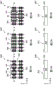
图3A、4A、5A、6A、7A、8A、9A、与10A是一些实施例中,以图2的方法形成的装置于多种工艺阶段的上视图。3A, 4A, 5A, 6A, 7A, 8A, 9A, and 10A are top views of devices formed by the method of FIG. 2 at various process stages in some embodiments.

图3B、4B、5B、6B、7B、8B、9B、与10B是一些实施例中,以图2的方法形成的装置于多种工艺阶段的剖视图。3B, 4B, 5B, 6B, 7B, 8B, 9B, and 10B are cross-sectional views of devices formed by the method of FIG. 2 at various process stages in some embodiments.

图11A与11B是本公开一实施例中,装置于方向性蚀刻工艺中的剖视图。11A and 11B are cross-sectional views of a device in a directional etching process according to an embodiment of the present disclosure.

图12是本公开一实施例中,另一集成电路设计的示意图。FIG. 12 is a schematic diagram of another integrated circuit design according to an embodiment of the present disclosure.

图13A、14A、15A、16A、17A、与18A是一些实施例中,以图2的方法形成的另一装置于多种工艺阶段的上视图。13A, 14A, 15A, 16A, 17A, and 18A are top views of another device formed by the method of FIG. 2 at various stages of processing in some embodiments.

图13B、14B、15B、16B、17B、与18B是一些实施例中,以图2的方法形成的另一装置于多种工艺阶段的剖视图。13B, 14B, 15B, 16B, 17B, and 18B are cross-sectional views of another device formed by the method of FIG. 2 at various process stages in some embodiments.

图19A、20A、21A、22A、23A、24A、25A、26A、与27A是一些实施例中,以图2的方法形成的又一装置于多种工艺阶段的上视图。19A, 20A, 21A, 22A, 23A, 24A, 25A, 26A, and 27A are top views of yet another device formed by the method of FIG. 2 at various process stages in some embodiments.

图19B、20B、21B、22B、23B、24B、25B、26B、与27B是一些实施例中,以图2的方法形成的又一装置于多种工艺阶段的剖视图。19B, 20B, 21B, 22B, 23B, 24B, 25B, 26B, and 27B are cross-sectional views of yet another device formed by the method of FIG. 2 at various process stages in some embodiments.

附图标记说明:Explanation of reference signs:

c1、c2、c3、c4、c5、c6 行c1, c2, c3, c4, c5, c6 rows

r1、r2、r3、r4 列r1, r2, r3, r4 columns

10 集成电路10 integrated circuits

12 主动区12 active area

14 栅极结构14 Gate structure

18、276 区块18, 276 blocks

18'、276' 凸角18', 276' lobe

18"、276" 凹角18", 276" concave corner

20、282、284 轮廓20, 282, 284 profiles

26、30 区域26, 30 areas

28 距离28 distance

100 方法100 ways

102、104、106、108、110、112、114 步骤102, 104, 106, 108, 110, 112, 114 steps

200、200'、200" 装置200, 200', 200" units

202 基板202 Substrate

204 硬遮罩层204 hard mask layer

206 光致抗蚀剂层206 photoresist layer

220 图案220 patterns

222、288、292 开口222, 288, 292 openings

250 等离子体离子束250 plasma ion beam

252 有效水平分量252 effective horizontal components

254 有效垂直分量254 effective vertical components

260 掺质260 dopant

272 栅极堆迭272 gate stack

273 栅极片段273 Gate Fragment

274 栅极接点274 Grid contacts

286、290 孔洞型图案286, 290 hole pattern

296 角落296 corners

具体实施方式Detailed ways

下述内容提供的不同实施例或实例可实施本公开的不同结构。特定构件与排列的实施例是用以简化本公开而非局限本公开。举例来说,形成第一构件于第二构件上的叙述包含两者直接接触,或两者之间隔有其他额外构件而非直接接触。此外,本公开的多种例子中可重复标号及/或符号,但这些重复仅用以简化与清楚说明,不代表不同实施例及/或设置之间具有相同标号及/或符号的单元之间具有相同的对应关系。Different embodiments or examples provided below may implement different structures of the present disclosure. The examples of specific components and arrangements are used to simplify the disclosure and not to limit it. For example, the statement that the first component is formed on the second component includes that the two are in direct contact, or there are other additional components interposed between the two instead of direct contact. In addition, the numbers and/or symbols may be repeated in various examples of the present disclosure, but these repetitions are only for simplification and clarity of description, and do not mean that units with the same number and/or symbols between different embodiments and/or configurations have the same correspondence.

此外,空间性的相对用语如「下方」、「其下」、「较下方」、「上方」、「较上方」、或类似用语可用于简化说明某一元件与另一元件在图示中的相对关系。空间性的相对用语可延伸至以其他方向使用的元件,而非局限于图示方向。元件亦可转动90°或其他角度,因此方向性用语仅用以说明图示中的方向。In addition, spatial relative terms such as "beneath", "beneath", "below", "above", "above", or similar terms may be used to simplify the relationship between one element and another element in the illustrations. relative relationship. Spatially relative terms may extend to elements used in other orientations and are not limited to the illustrated orientation. Components may also be rotated by 90° or other angles, so directional terms are used only to describe directions in the drawings.

图1是本公开一实施例中,集成电路10的布局图。如图1所示,布局10包含多个主动区12,其沿着X方向纵向定向;以及多个栅极结构14,其沿着Y方向纵向定向,且X方向垂直于Y方向。主动区12与栅极结构14的每一交会处形成场效晶体管。在一实施例中,主动区12为鳍状,而形成其上的场效晶体管为鳍状场效晶体管。图1所示的例子具有四列(r1、r2、r3、与r4)的主动区12与六行(c1、c2、c3、c4、c5、与c6)的栅极结构14,两者共同形成24个场效晶体管。在一些设计中,需要一些晶体管的物理特性及/或电性不同于其他晶体管。举例来说,区块18中的晶体管(第一型晶体管)其临界电压不同于区块18外的晶体管(第二型晶体管)。举例来说,第一型晶体管设计为具有高临界电压,而第二型晶体管设计为具有低临界电压。上述设计为静态随机存取记忆单元设计及/或外围电路设计所需。FIG. 1 is a layout diagram of an integrated circuit 10 in an embodiment of the present disclosure. As shown in FIG. 1 , the layout 10 includes a plurality of active regions 12 longitudinally oriented along the X direction; and a plurality of gate structures 14 longitudinally oriented along the Y direction, and the X direction is perpendicular to the Y direction. Each intersection of the active region 12 and the gate structure 14 forms a field effect transistor. In one embodiment, the active region 12 is fin-shaped, and the field effect transistors formed thereon are fin-shaped field effect transistors. The example shown in FIG. 1 has four columns (r1, r2, r3, and r4) of active regions 12 and six rows (c1, c2, c3, c4, c5, and c6) of gate structures 14, which together form 24 field effect transistors. In some designs, it is desired that some transistors be physically and/or electrically different from other transistors. For example, transistors in block 18 (type 1 transistors) have different threshold voltages than transistors outside block 18 (type 2 transistors). For example, the first type transistor is designed to have a high threshold voltage, and the second type transistor is designed to have a low threshold voltage. The above design is required for SRAM unit design and/or peripheral circuit design.

为实施集成电路10,方法之一为形成遮罩单元覆盖第二型晶体管,并露出第一型晶体管以进行工艺;或者形成遮罩单元覆盖第一型晶体管,并露出第二型晶体管以进行工艺。上述工艺可为离子布植。遮罩单元可包含光致抗蚀剂材料或硬遮罩材料,其可由光微影工艺形成。区块18的边界可位于相邻结构的中间处,比如水平地位于栅极结构14之间,以及垂直地位于主动区12之间。在图1所示的例子中,区块18包含六个直角凸角(外侧角落)18',以及两个直角凹角(内侧角落)18"。凸角指的是区域的角落,其为两线段交会的顶点,且连接两个线段上任一对点的直线是位于区域中。凹角指的是区域的角落,其为两线段交会的顶点,且连接两个线段上任一对点的直线位于区域之外。之后将说明光微影工艺后,凹角或凸角均会圆润化。为简化说明,圆润的凹角与圆润的凸角仍分别称作凹角与凸角。在多种实施例中,区块18的形状可比图1所示的形状简单或复杂。区块18的形状为光微影工艺将形成的例示性目标图案。In order to implement the integrated circuit 10, one of the methods is to form a mask unit to cover the second type transistor and expose the first type transistor for process; or form a mask unit to cover the first type transistor and expose the second type transistor for process . The above process can be ion implantation. The mask unit may include a photoresist material or a hard mask material, which may be formed by a photolithography process. The boundaries of the blocks 18 may be located in the middle of adjacent structures, such as horizontally between the gate structures 14 and vertically between the active regions 12 . In the example shown in Figure 1, the block 18 contains six right-angle convex corners (outer corners) 18', and two right-angle concave corners (inner corners) 18". A convex corner refers to a corner of an area, which is two line segments The vertex where two line segments meet and the line connecting any pair of points on the two line segments lies in the region. A concave corner refers to the corner of the region, which is the vertex where the two line segments meet and the line connecting any pair of points on the two line segments lies between the region Outside. After the light lithography process will be explained later, the concave corner or the convex corner will be rounded. To simplify the description, the rounded concave corner and the rounded convex corner are still called concave corners and convex corners respectively. In various embodiments, the block The shape of 18 may be simpler or more complex than that shown in Figure 1. The shape of block 18 is an exemplary target pattern to be formed by the photolithography process.

理想状态下,实际上的遮罩单元与目标图案(如区块18)的尺寸一致。然而光微影工艺中的光学效应及/或蚀刻偏差,通常会让遮罩单元不符目标图案。相反地,实际的遮罩单元其轮廓20具有圆润的角落,因此遮罩单元的边界靠近一些集成电路结构,特别是在凹角18"。缩小的距离即为失去的设计余裕。图1亦显示围绕晶体管的区域26。区域26指的是遮罩单元的轮廓20不可接触的区域。举例来说,区域26可用于工艺变异如关键尺寸变异与覆盖变异。凹角18"其轮廓20与区域26之间的距离,通常小于凸角18'其轮廓20与区域26之间的距离。轮廓20与区域26之间的最小距离即设计余裕,比如图1的例子所示的距离28。图1亦显示围绕晶体管的区域30。区域30即遮罩单元的轮廓必需围绕的区域。由于集成电路的尺寸持续缩小,越来越需要实际的遮罩单元其轮廓20不具凹角的形成方法,比如在整个微影图案化工艺中,将目标图案(如区块18)转换成一组不具凹角的子图案,以符合特定区域(比如区域26与30)对遮罩与非遮罩的需求。本公开提供一或多个实施例以解决微影图案化工艺中凹角圆润化的问题。这些实施例可用于多种集成电路设计,比如搭配集成电路10或替代集成电路10的设计。Ideally, the actual mask unit has the same size as the target pattern (such as the block 18 ). However, optical effects and/or etch deviations in the photolithography process usually make the mask elements not conform to the target pattern. In contrast, the actual mask cell outline 20 has rounded corners, so the mask cell boundaries are close to some integrated circuit structures, especially at the concave corner 18". The reduced distance is the lost design margin. Fig. 1 also shows the surrounding The area 26 of the transistor. The area 26 refers to the area where the outline 20 of the mask unit is inaccessible. For example, the area 26 can be used for process variation such as critical dimension variation and coverage variation. The recessed corner 18" between the outline 20 and the area 26 is generally less than the distance between the contour 20 of the lobe 18' and the region 26. The minimum distance between contour 20 and region 26 is the design margin, such as distance 28 shown in the example of FIG. 1 . Figure 1 also shows a region 30 surrounding the transistor. The area 30 is the area that the outline of the mask unit must surround. As the size of integrated circuits continues to shrink, there is an increasing need for an actual mask element whose outline 20 is formed without reentrant corners, such as converting a target pattern (such as a block 18 ) into a set of non-retentive corners throughout the lithographic patterning process. sub-patterns to meet the masking and non-masking requirements of specific areas (such as areas 26 and 30). The present disclosure provides one or more embodiments to address the problem of reentrant corner rounding in lithographic patterning processes. These embodiments can be used in various integrated circuit designs, such as designs that accompany integrated circuit 10 or replace integrated circuit 10 .

如图2所示,方法100的流程图用于形成孔洞型图案,其通过方向性蚀刻技术具有多个孔洞(或开口)而不具凹角。方法100仅用以举例,而非局限本公开至权利要求未实际限缩的部分。在方法100之前、之中、或之后可进行额外步骤,且方法的其他实施例可置换、省略、或调换一些上述步骤。As shown in FIG. 2 , the flowchart of the method 100 is used to form a hole-type pattern, which has a plurality of holes (or openings) without concave corners by directional etching technology. The method 100 is used as an example only, and does not limit the disclosure to the part where the claims do not actually limit. Additional steps may be performed before, during, or after method 100, and other embodiments of the method may substitute, omit, or swap some of the steps described above.

在多种实施例中,方法100形成多个开口露出部分的装置结构以进行后续处理(如蚀刻或离子布植),接着施加方向性蚀刻以扩大每一开口,直到完全露出装置结构。在一些实施例中,每一开口的形状可为具有圆润角落的实质上矩形,以避免孔洞型图案中的凹角。此外,方法100可用以形成孔洞型光致抗蚀剂图案或孔洞型硬遮罩图案。图3A至10A及图3B至10B分别为装置200于方法100的第一实施例的多种工艺步骤中的上视图与剖视图,其中具有凹角的目标孔洞型图案调整为不具有凹角的孔洞型图案,且对孔洞型光致抗蚀剂图案进行方向性蚀刻工艺。图11A与11B是例示性的方向性蚀刻工艺。图12、图13A至18A、与图13B至18B分别为装置200'于方法100的第二实施例的多种工艺步骤中的上视图与剖视图,其依据装置结构的几何形状与位置形成孔洞型光致抗蚀剂图案,并省略方法100的步骤106与108。图19A至27A与图19B至27B分别为装置200"于方法100的第三实施例的多种工艺步骤中的上视图与剖视图,其依据装置结构的几何形状与位置形成孔洞型硬遮罩图案,并施加方向性蚀刻工艺至孔洞型硬遮罩图案。在多种实施例中,光微影工艺的方向性蚀刻可分别施加至光致抗蚀剂图案与硬遮罩图案,或者同时施加至光致抗蚀剂图案与硬遮罩图案。举例来说,光微影工艺可依据方法100的实施例,只处理光致抗蚀剂图案、只处理硬遮罩图案、或者处理光致抗蚀剂图案与硬遮罩图案。方法100将搭配图2、图3A至10A、与图3B至10B说明如下。In various embodiments, method 100 forms a plurality of openings exposing portions of the device structure for subsequent processing such as etching or ion implantation, and then applies directional etching to enlarge each opening until the device structure is fully exposed. In some embodiments, the shape of each opening may be substantially rectangular with rounded corners to avoid concave corners in hole-type patterns. In addition, the method 100 can be used to form a hole-type photoresist pattern or a hole-type hard mask pattern. FIGS. 3A to 10A and FIGS. 3B to 10B are respectively a top view and a cross-sectional view of the device 200 in various process steps of the first embodiment of the method 100, wherein the target hole pattern with concave corners is adjusted to a hole pattern without concave corners. , and perform a directional etching process on the hole-type photoresist pattern. 11A and 11B are exemplary directional etching processes. Figure 12, Figures 13A to 18A, and Figures 13B to 18B are respectively a top view and a cross-sectional view of the device 200' in various process steps of the second embodiment of the method 100, which form holes according to the geometry and position of the device structure photoresist pattern, and steps 106 and 108 of method 100 are omitted. FIGS. 19A to 27A and FIGS. 19B to 27B are respectively a top view and a cross-sectional view of a device 200" in various process steps of the third embodiment of the method 100, which form a hole-type hard mask pattern according to the geometry and position of the device structure. , and apply a directional etching process to the hole-type hard mask pattern. In various embodiments, the directional etching of the photolithography process can be applied to the photoresist pattern and the hard mask pattern separately, or applied to the A photoresist pattern and a hard mask pattern. For example, the photolithography process can process only the photoresist pattern, only the hard mask pattern, or process the photoresist according to an embodiment of the method 100. The agent pattern and the hard mask pattern. The method 100 will be described with reference to FIG. 2 , FIGS. 3A to 10A , and FIGS. 3B to 10B as follows.

在步骤102中,方法100(见图2)提供基板202(见图3A与3B)。在多种实施例中,基板202包含一或多个材料层,且可处于装置200的形成工艺的中间步骤。装置200可为集成电路,装置200可为集成电路或其部分,其可包含静态随机存取存储器存储器及/或其他逻辑电路,被动构件如电阻、电容、或电感,或主动构件如p型场效晶体管、n型场效晶体管、金氧半场效晶体管、互补式金氧半晶体管、双极晶体管、高压晶体管、高频晶体管、其他记忆单元、或上述的组合。装置200可包含三维装置与多闸装置,比如双闸场效晶体管、鳍状场效晶体管、三闸场效晶体管、Ω-场效晶体管、栅极全绕装置、或垂直栅极全绕装置。在一实施例中,基板202为半导体基板如晶圆。在一实施例中,基板202包含结晶结构的硅。在其他实施例中,基板202包含其他半导体元素如锗、或半导体化合物如碳化硅、砷化镓、砷化铟、或磷化铟。基板202可包含绝缘层上硅基板、可具有应力以增进效能、可包含磊晶区、可包含隔离区、可包含掺杂区、可包含一或多个半导体装置或其部分、可包含导电及/或非导电层、及/或可包含其他合适的结构与层状物。In step 102, method 100 (see FIG. 2) provides substrate 202 (see FIGS. 3A and 3B). In various embodiments, the substrate 202 includes one or more material layers and may be an intermediate step in the formation process of the device 200 . Device 200 may be an integrated circuit. Device 200 may be an integrated circuit or portion thereof, which may include SRAM memory and/or other logic circuits, passive components such as resistors, capacitors, or inductors, or active components such as p-type field effect transistors, n-type field effect transistors, metal oxide semiconductor field effect transistors, complementary metal oxide semiconductor transistors, bipolar transistors, high voltage transistors, high frequency transistors, other memory units, or combinations thereof. The device 200 may include three-dimensional devices and multi-gate devices, such as double gate field effect transistors, fin field effect transistors, triple gate field effect transistors, Ω-field effect transistors, all-around-gate devices, or all-around-gate vertical devices. In one embodiment, the substrate 202 is a semiconductor substrate such as a wafer. In one embodiment, the substrate 202 includes silicon in a crystalline structure. In other embodiments, the substrate 202 includes other semiconductor elements such as germanium, or semiconductor compounds such as silicon carbide, gallium arsenide, indium arsenide, or indium phosphide. Substrate 202 may include a silicon-on-insulator substrate, may be stressed to enhance performance, may include epitaxial regions, may include isolation regions, may include doped regions, may include one or more semiconductor devices or portions thereof, may include conductive and and/or non-conductive layers, and/or may include other suitable structures and layers.

装置200在许多方面可与图1的集成电路10实质上类似。装置200具有多个主动区12,其沿着X方向纵向定向;以及多个栅极结构14,其沿着Y方向纵向定向,且X方向垂直于Y方向。场效晶体管(如鳍状场效晶体管)形成于主动区12与栅极结构14的每一交会处。区域30为需要额外处理(如离子布植)的场效晶体管结构,而区域26为不需额外处理(用于区域30)的场效晶体管结构。Device 200 may be substantially similar to integrated circuit 10 of FIG. 1 in many respects. The device 200 has a plurality of active regions 12 longitudinally oriented along the X direction, and a plurality of gate structures 14 longitudinally oriented along the Y direction, with the X direction being perpendicular to the Y direction. Field effect transistors, such as FinFETs, are formed at each intersection of the active region 12 and the gate structure 14 . Region 30 is a FET structure that requires additional processing (eg, ion implantation), while region 26 is a FET structure that does not require additional processing (for region 30 ).

在步骤104中,方法100(见图2)形成图案化层于基板202上。图案化层亦可包含多个材料层。在图4A与4B所示的此实施例中,步骤104形成硬遮罩层204于基板202上,并形成光致抗蚀剂层206于硬遮罩层204上。在多种实施例中,可在光致抗蚀剂层206与硬遮罩层204之间新增其他材料层。在一些实施例中,亦可在硬遮罩层204与基板202之间新增其他材料层。In step 104 , method 100 (see FIG. 2 ) forms a patterned layer on substrate 202 . The patterned layer can also include multiple material layers. In the embodiment shown in FIGS. 4A and 4B , step 104 forms a hard mask layer 204 on the substrate 202 , and forms a photoresist layer 206 on the hard mask layer 204 . In various embodiments, additional material layers may be added between the photoresist layer 206 and the hard mask layer 204 . In some embodiments, other material layers may also be added between the hard mask layer 204 and the substrate 202 .

硬遮罩层204可包含非晶硅、氧化硅、氮化硅、氮化钛、氮氧化硅、氮化碳硅、或其他合适材料或组成,且其形成方法可为化学气相沉积、低压化学气相沉积、等离子体增强化学气相沉积、物理气相沉积、原子层沉积、或其他合适的沉积方法。The hard mask layer 204 may comprise amorphous silicon, silicon oxide, silicon nitride, titanium nitride, silicon oxynitride, silicon carbon nitride, or other suitable materials or compositions, and its formation method may be chemical vapor deposition, low pressure chemical Vapor deposition, plasma enhanced chemical vapor deposition, physical vapor deposition, atomic layer deposition, or other suitable deposition methods.

在一实施例中,光致抗蚀剂层206的形成方法为旋转涂布工艺后进行软烘烤工艺。光致抗蚀剂层可为正光致抗蚀剂或负光致抗蚀剂。正光致抗蚀剂通常不溶于光致抗蚀剂显影剂中,但经射线如深紫外线或极紫外线曝光后转为可溶。例示性的正光致抗蚀剂材料为化学放大光致抗蚀剂。负光致抗蚀剂具有相反特性:通常溶于光致抗蚀剂显影剂中,但经射线如深紫外线或极紫外线曝光后转为不可溶。例示性的负光致抗蚀剂材料为聚合物,其经曝光后可形成分子内交联及/或分子间交联。上述聚合物可由乙基(α-羟基)丙烯酸酯与甲基丙烯酸聚合而成。In one embodiment, the photoresist layer 206 is formed by a spin-coating process followed by a soft-baking process. The photoresist layer can be a positive photoresist or a negative photoresist. Positive photoresists are generally insoluble in photoresist developers, but become soluble after exposure to radiation such as deep ultraviolet or extreme ultraviolet rays. An exemplary positive photoresist material is a chemically amplified photoresist. Negative photoresists have the opposite properties: they are usually soluble in the photoresist developer, but become insoluble upon exposure to radiation such as deep or extreme ultraviolet rays. Exemplary negative photoresist materials are polymers that form intramolecular and/or intermolecular crosslinks upon exposure. The aforementioned polymers can be polymerized from ethyl (α-hydroxy) acrylate and methacrylic acid.

在步骤106中,方法100(见图2)提供目标图案如区块18,其形成于图案化层中(见图5A与5B)。区块18对应具有至少一开口的孔洞型图案。在此实施例中,区块18包含一开口。若图案化层依据区块18图案化,则形成的开口将完全露出基板202中需要额外处理的区域(如区域30),而图案化层仍覆盖其下方的其他区域(如区域26)。由于区域26与30的几何尺寸与位置,定义于区块18中的开口将具有多个凸角18'与至少一凹角18"。若将开口转移至图案化层,则光微影工艺中的光学效应及/或蚀刻偏差会使凸角与凹角圆润化。圆润的凹角18"会造成开口轮廓更靠近区域26,即减少设计余裕。In step 106, method 100 (see FIG. 2) provides a target pattern, such as a block 18, formed in a patterned layer (see FIGS. 5A and 5B). The block 18 corresponds to a hole pattern having at least one opening. In this embodiment, block 18 includes an opening. If the patterned layer is patterned according to the block 18 , the formed opening will completely expose the area of the substrate 202 that requires additional processing (eg, area 30 ), while the patterned layer still covers other areas (eg, area 26 ) thereunder. Due to the geometry and location of regions 26 and 30, the openings defined in block 18 will have a plurality of convex corners 18' and at least one concave corner 18". If the openings are transferred to the patterned layer, the Optical effects and/or etch deviations can round the convex and concave corners. The rounded concave corners 18" will cause the opening profile to be closer to the region 26, ie reduce the design margin.

如图5A与5B所示的步骤108中,方法100(见图2)将区块18转为改良图案,比如此实施例中的图案220。定义于区块18中的开口将改为图案220中的多个开口(或孔洞)222。开口222不具有凹角。举例来说,一些实施例中的开口形状为圆形、方形、或矩形。改良的图案220中的开口,可覆盖定义于区块18中的部分开口区域。开口222露出部分的区域30。In step 108 shown in FIGS. 5A and 5B , method 100 (see FIG. 2 ) converts block 18 into a modified pattern, such as pattern 220 in this embodiment. The openings defined in block 18 are replaced by a plurality of openings (or holes) 222 in pattern 220 . The opening 222 has no concave corners. For example, the shape of the opening in some embodiments is circular, square, or rectangular. The openings in the improved pattern 220 can cover part of the opening area defined in the block 18 . The opening 222 exposes a portion of the area 30 .

在步骤110中,方法100(见图2)形成一或多个孔洞型图案于图案化层中,且一或多个孔洞型图案包含图案220(见图6A与6B)。在此实施例中,图案220中的开口222转移至光致抗蚀剂层206。为了简化附图,形成于光致抗蚀剂层206中的个别开口仍称作开口222。在一实施例中,图案化光致抗蚀剂层206的步骤包括以射线曝光光致抗蚀剂层206、曝光后烘烤、在显影剂中显影光致抗蚀剂层206、以及硬烘烤,以移除光致抗蚀剂层206的曝光部分(或未曝光部分,若采用负光致抗蚀剂)。保留的部分光致抗蚀剂层206成为具有开口222的光致抗蚀剂图案。开口222可具有实质上矩形的上视形状。由于曝光工艺的光学效应等因素,形成于光致抗蚀剂层206中的开口222其上视形状将圆润化。然而开口222只具有凸角,因此圆润化的角落不会劣化开口222与区域26之间的设计余裕。每一开口222可具有实质上相同的尺寸。由于开口222的位置与尺寸,一实施例中的每一开口222完全露出至少一区域30;另一实施例中的每一开口222露出至少一区域且部分地露出至少另一区域30、且又一实施例中的每一开口222只部分地露出一或两个区域30。In step 110 , method 100 (see FIG. 2 ) forms one or more hole-type patterns in the patterned layer, and the one or more hole-type patterns include pattern 220 (see FIGS. 6A and 6B ). In this embodiment, openings 222 in pattern 220 are transferred to photoresist layer 206 . To simplify the drawing, the individual openings formed in the photoresist layer 206 are still referred to as openings 222 . In one embodiment, the step of patterning the photoresist layer 206 includes exposing the photoresist layer 206 to radiation, post-exposure baking, developing the photoresist layer 206 in a developer, and hard baking. Bake to remove exposed portions of the photoresist layer 206 (or unexposed portions, if a negative photoresist is used). The remaining part of the photoresist layer 206 becomes a photoresist pattern with openings 222 . The opening 222 may have a substantially rectangular top-view shape. Due to factors such as the optical effect of the exposure process, the top view shape of the opening 222 formed in the photoresist layer 206 will be rounded. However, the opening 222 only has convex corners, so the rounded corners will not degrade the design margin between the opening 222 and the region 26 . Each opening 222 may have substantially the same size. Due to the location and size of the openings 222, each opening 222 in one embodiment fully exposes at least one region 30; each opening 222 in another embodiment exposes at least one region and partially exposes at least another region 30, and in turn In one embodiment, each opening 222 only partially exposes one or two regions 30 .

在步骤112中,方法100(见图2)沿着一方向对开口222的内侧壁进行方向性蚀刻。如图7A与7B所示的实施例,区域30沿着Y方向纵向延伸,而方向性蚀刻沿着X方向进行,且X方向垂直于Y方向。在一些实施例中,方向性蚀刻对光致抗蚀剂层206具有选择性,且不蚀刻(至少不明显地蚀刻)硬遮罩层204。In step 112 , the method 100 (see FIG. 2 ) performs directional etching on the inner sidewall of the opening 222 along a direction. In the embodiment shown in FIGS. 7A and 7B , the region 30 extends longitudinally along the Y direction, and the directional etching proceeds along the X direction, and the X direction is perpendicular to the Y direction. In some embodiments, the directional etch is selective to the photoresist layer 206 and does not etch (at least not significantly etches) the hard mask layer 204 .

开口222的内侧壁可沿着方向性蚀刻的方向扩大,且此蚀刻方向位于与基板202的上表面平行的平面中。在多种实施例中,放向性蚀刻亦具有垂直参数,比如沿着Z方向,且Z方向垂直于基板202的上表面。在一实施例中,步骤112可包含斜向的等离子体蚀刻工艺,其朝着X或Y方向偏向。图11A与11B显示斜向等离子体蚀刻工艺的例子。如图11A所示,等离子体离子束250自Z方向倾斜,因此具有有效水平分量252与有效垂直分量254。在一实施例中,等离子体离子束250可包含氩离子。在其他实施例中,等离子体离子束250可包含氦、硅烷、甲烷、氧、氮、二氧化碳、或上述的组合。装置200可嵌置于晶圆站点上,并沿着X方向、Y方向、或垂直于Z方向的另一方向扫描装置200。当晶圆站点移动时,等离子体离子束250维持相同角度(或角分布)。在图11A所示的例子中,等离子体离子束250具有单峰角分布。在图11B所示的例子中,等离子体离子束250具有双峰角分布,其中等离子体离子束250同时沿着两方向蚀刻光致抗蚀剂层206的图案。通过调整等离子体离子束250的入射角与角分布,可良好地控制水平方向(沿着X及/或Y方向)的蚀刻速率。The inner sidewall of the opening 222 can expand along the direction of the directional etching, and the etching direction is in a plane parallel to the upper surface of the substrate 202 . In various embodiments, the directional etch also has a vertical parameter, such as along the Z direction, and the Z direction is perpendicular to the top surface of the substrate 202 . In one embodiment, step 112 may include an oblique plasma etch process, which is biased toward the X or Y direction. 11A and 11B show an example of an oblique plasma etch process. As shown in FIG. 11A , the plasma ion beam 250 is tilted from the Z direction and thus has an effective horizontal component 252 and an effective vertical component 254 . In one embodiment, plasma ion beam 250 may contain argon ions. In other embodiments, plasma ion beam 250 may contain helium, silane, methane, oxygen, nitrogen, carbon dioxide, or combinations thereof. The device 200 can be embedded on a wafer site, and the device 200 can be scanned along the X direction, the Y direction, or another direction perpendicular to the Z direction. The plasma ion beam 250 maintains the same angle (or angular distribution) as the wafer site moves. In the example shown in FIG. 11A, plasma ion beam 250 has a single-peak angular distribution. In the example shown in FIG. 11B , the plasma ion beam 250 has a bimodal angular distribution, wherein the plasma ion beam 250 simultaneously etches the pattern of the photoresist layer 206 in two directions. By adjusting the incident angle and angular distribution of the plasma ion beam 250, the etching rate in the horizontal direction (along the X and/or Y directions) can be well controlled.

如图8A与8B所示,在方向性蚀刻之后,可沿着方向性蚀刻的方向扩大开口222。开口222在扩大后,可称作扩大的开口或延伸的开口。在一些实施例中,扩大的开口222具有实质上相同的尺寸。在一些实施例中,每一扩大的开口222的上视形状为具有圆润角落的实质上矩形。此外,每一扩大的开口222可具有沿着方向性蚀刻的方向纵向延伸的中间线,且至少两个扩大的开口222的中间线未对准(即非共线性),比如图8A所示的两个扩大的开口222。一些扩大的开口222在扩大后可彼此合并。在图8A所示的例子中,两个扩大的开口222仍维持彼此分离。As shown in FIGS. 8A and 8B , after the directional etching, the opening 222 may be enlarged along the direction of the directional etching. After the opening 222 is enlarged, it may be referred to as an enlarged opening or an extended opening. In some embodiments, enlarged openings 222 have substantially the same size. In some embodiments, the top-view shape of each enlarged opening 222 is substantially rectangular with rounded corners. In addition, each enlarged opening 222 may have a median line extending longitudinally along the direction of directional etching, and the median lines of at least two enlarged openings 222 are misaligned (ie, non-collinear), such as shown in FIG. 8A Two enlarged openings 222 . Some of the enlarged openings 222 may merge with each other after being enlarged. In the example shown in FIG. 8A, the two enlarged openings 222 remain separated from each other.

与定义于目标图案18中的开口相较,扩大的开口222只露出一部分定义于目标图案18中的开口。图案化层仍覆盖扩大的开口222之间的部份基板202。与此同时,一些实施例中扩大的开口222完全露出区域30。每一区域30完全露出于开口222之一中,且在后续步骤中可经由开口222对区域30进行额外处理。由于扩大的开口222中不具有凹角,因此可维持设计余裕并增加图案保真度。Compared with the openings defined in the target pattern 18 , the enlarged openings 222 expose only a portion of the openings defined in the target pattern 18 . The patterned layer still covers the portion of the substrate 202 between the enlarged openings 222 . At the same time, enlarged opening 222 in some embodiments fully exposes region 30 . Each region 30 is fully exposed in one of the openings 222 , and additional processing can be performed on the region 30 through the opening 222 in subsequent steps. Since there are no reentrant corners in the enlarged opening 222, design margins are maintained and pattern fidelity is increased.

如图9A与9B所示,步骤112可还包含将光致抗蚀剂层206中扩大的开口222转移至硬遮罩层204。采用图案化的光致抗蚀剂层206作为蚀刻遮罩,并蚀刻硬遮罩层204。举例来说,硬遮罩层204的蚀刻方法可为湿蚀刻工艺、干蚀刻工艺、原子层蚀刻工艺、或其他合适的蚀刻工艺。蚀刻工艺可消耗部分的光致抗蚀剂层206。蚀刻后若残留任何的光致抗蚀剂层206,可采用光致抗蚀剂剥除工艺移除。As shown in FIGS. 9A and 9B , step 112 may further include transferring the enlarged opening 222 in the photoresist layer 206 to the hard mask layer 204 . The patterned photoresist layer 206 is used as an etch mask, and the hard mask layer 204 is etched. For example, the etching method of the hard mask layer 204 may be a wet etching process, a dry etching process, an atomic layer etching process, or other suitable etching processes. The etching process may consume portions of the photoresist layer 206 . If any photoresist layer 206 remains after etching, it can be removed by a photoresist stripping process.

在步骤114中,方法100(见图2)采用硬遮罩层204中扩大的开口222,对区域30(见图10A与10B)进行进行额外处理。在一些实施例中,方法100采用图案化的硬遮罩层204作为离子布植遮罩,以将掺质260布植至区域30中。硬遮罩层204覆盖的区域26仍实质上不含掺质260。在另一实施例中,方法100(见图2)采用图案化的光致抗蚀剂层206作为离子布植遮罩。举例来说,方法100可形成光致抗蚀剂层206于基板202上,并省略硬遮罩层204。在曝光与显影光致抗蚀剂层206后,可进一步对光致抗蚀剂层206进行前述的方向性蚀刻工艺。之后对基板202进行离子布植工艺时,图案化的光致抗蚀剂层206可作为遮罩单元。In step 114 , method 100 (see FIG. 2 ) performs additional processing on region 30 (see FIGS. 10A and 10B ) using enlarged opening 222 in hard mask layer 204 . In some embodiments, method 100 uses patterned hard mask layer 204 as an ion implantation mask to implant dopants 260 into region 30 . Region 26 covered by hard mask layer 204 remains substantially free of dopants 260 . In another embodiment, method 100 (see FIG. 2 ) employs patterned photoresist layer 206 as an ion implantation mask. For example, the method 100 can form the photoresist layer 206 on the substrate 202 and omit the hard mask layer 204 . After the photoresist layer 206 is exposed and developed, the aforementioned directional etching process can be further performed on the photoresist layer 206 . When the ion implantation process is performed on the substrate 202 later, the patterned photoresist layer 206 can be used as a mask unit.

图12、图13A至18A、与图13B至18B分别为装置200'于方法100的第二实施例的多种工艺步骤中的上视图与剖视图,其略过方法100的步骤106与108。此实施例有许多方面与图1、图3A至10A、及图3B至10B所述的内容类似。12 , FIGS. 13A-18A , and FIGS. 13B-18B are top and cross-sectional views, respectively, of device 200 ′ during various process steps of a second embodiment of method 100 , which skips steps 106 and 108 of method 100 . This embodiment is similar to that described in FIG. 1 , FIGS. 3A-10A , and FIGS. 3B-10B in many respects.

如图12所示,装置200'包含多个栅极结构272,其沿着Y方向纵向定向。在一实施例中,每一栅极结构272具有需额外处理的栅极片段273。额外处理可为栅极切割工艺,其自对应的栅极结构272移除栅极片段273,并将栅极结构272分隔成多个不相连的片段。在一些设计中,一或多个栅极结构272可具有额外结构,比如图12的例子所示的栅极接点274。在栅极切割工艺中,栅极接点274可维持不变。为实施装置200',方法之一为形成遮罩单元以覆盖栅极片段273以外的栅极堆迭272与栅极接点274,并经由遮罩单元中的开口露出栅极片段273以进行工艺。举例来说,区块276为遮罩单元中的开口。栅极接点274为区块276未接触的区域。为了适用于相邻结构,区块276可包含多个直角的凸角276'与至少一直角的凹角276"。区块276的形状为光微影工艺形成的目标图案。由于光微影工艺的光学效应及/或蚀刻偏差,遮罩单元通常无法正确地符合目标图案。举例来说,遮罩单元可包含光致抗蚀剂层与硬遮罩层。轮廓282指的是曝光与显影光致抗蚀剂后,形成于光致抗蚀剂层中的开口(比如显影后检查的轮廓)。轮廓284指的是将光致抗蚀剂层中的开口转移至硬遮罩层后的开口(比如蚀刻后检查的轮廓)。形成于遮罩单元中的实际开口的轮廓282与284,其上视图均具有圆润的角落。特别是硬遮罩层中的轮廓284,由于处理栅极片段273的步骤可采用图案化的硬遮罩层作为蚀刻遮罩,栅极接点274需位于轮廓284之外。圆润的凹角会让遮罩单元的边界更靠近需维持覆盖的结构,因此会缩小设计余裕。目前需要新的方法形成开口于遮罩单元中,其不具凹角且在整个光微影工艺中符合特定区域(比如栅极接点274与栅极片段273)的遮罩与未遮罩需求。As shown in FIG. 12, device 200' includes a plurality of gate structures 272 that are longitudinally oriented along the Y direction. In one embodiment, each gate structure 272 has a gate segment 273 that requires additional processing. The additional processing may be a gate cutting process that removes the gate segments 273 from the corresponding gate structures 272 and separates the gate structures 272 into a plurality of disconnected segments. In some designs, one or more gate structures 272 may have additional structures, such as gate contacts 274 shown in the example of FIG. 12 . During the gate cutting process, the gate contact 274 may remain unchanged. To implement the device 200 ′, one of the methods is to form a mask unit to cover the gate stack 272 and the gate contact 274 other than the gate segment 273 , and expose the gate segment 273 through an opening in the mask unit for processing. For example, block 276 is an opening in the mask unit. Gate contact 274 is the untouched area of block 276 . In order to be suitable for adjacent structures, the block 276 may include a plurality of right-angled convex corners 276' and at least a right-angled concave corner 276". The shape of the block 276 is the target pattern formed by the photolithography process. Due to the Due to optical effects and/or etch deviations, mask elements often do not conform to the target pattern correctly. For example, a mask element may include a photoresist layer and a hard mask layer. Outline 282 refers to the exposure and development photoresist After resist, the openings formed in the photoresist layer (such as contours for inspection after development). The contour 284 refers to the openings in the photoresist layer that are transferred to the openings after the hard mask layer ( Such as the outline of the post-etch inspection). The outlines 282 and 284 of the actual opening formed in the mask unit have rounded corners in the top view. Especially the outline 284 in the hard mask layer, due to the processing of the gate segment 273 The step can use a patterned hard mask layer as an etching mask, and the gate contact 274 needs to be located outside the outline 284. The rounded concave corner will make the boundary of the mask cell closer to the structure that needs to maintain coverage, thus reducing the design margin. There is a need for new methods of forming openings in masked units that do not have concave corners and that meet the masked and unmasked requirements of specific regions (eg, gate contacts 274 and gate segments 273 ) throughout the photolithography process.

如图13A与13B所示,方法100的步骤102提供基板202。在多种实施例中,基板202包含一或多个材料层,且可处于装置200'的形成工艺其中间阶段。装置200'包含多个栅极堆迭272。每一栅极堆迭272具有栅极片段273,且后续的栅极切割工艺将移除栅极片段273。栅极堆迭272的一者还包含栅极接点274形成其上。As shown in FIGS. 13A and 13B , step 102 of method 100 provides a substrate 202 . In various embodiments, the substrate 202 includes one or more material layers and may be at an intermediate stage in the formation process of the device 200'. Device 200 ′ includes a plurality of gate stacks 272 . Each gate stack 272 has a gate segment 273 and a subsequent gate cutting process will remove the gate segment 273 . One of the gate stacks 272 also includes a gate contact 274 formed thereon.

如图14A与14B所示,方法100的步骤104形成图案化层于基板202上。图案化层可还包含多个材料层,比如硬遮罩层204,以及硬遮罩层204上的光致抗蚀剂层206。As shown in FIGS. 14A and 14B , step 104 of method 100 forms a patterned layer on substrate 202 . The patterned layer may also include multiple material layers, such as a hard mask layer 204 , and a photoresist layer 206 on the hard mask layer 204 .

如图15A与15B所示,方法100的步骤110形成孔洞型图案286,其包含多个开口288。在一些实施例中,可视情况进行或省略方法100中的步骤106与108。孔洞型图案286可取决于需露出的结构(如栅极片段273)的几何形状与位置,而不需由初始的目标图案开始。在图15A与15B中的实施例,先将孔洞型图案286转移至光致抗蚀剂层206。开口288形成于每一栅极片段273上。开口288露出部分的栅极片段273。在一例中,在Y方向上的开口288其尺寸大于栅极片段273,但在X方向上的开口288其尺寸小于栅极片段273。开口288不具有凹角。举例来说,开口288的上视形状可为圆形、方形、矩形。在一例中,每一开口288具有实质上相同的形状与尺寸,比如具有圆润角落的矩形。As shown in FIGS. 15A and 15B , step 110 of method 100 forms a hole-type pattern 286 including a plurality of openings 288 . In some embodiments, steps 106 and 108 in method 100 may be performed or omitted as appropriate. The hole-type pattern 286 may depend on the geometry and location of the structure to be exposed (eg, the gate segment 273 ) without starting from an initial target pattern. In the embodiment of FIGS. 15A and 15B , the hole-type pattern 286 is first transferred to the photoresist layer 206 . An opening 288 is formed on each gate segment 273 . The opening 288 exposes a portion of the gate segment 273 . In one example, the size of the opening 288 in the Y direction is larger than that of the gate segment 273 , but the size of the opening 288 in the X direction is smaller than that of the gate segment 273 . Opening 288 has no concave corners. For example, the top view shape of the opening 288 can be circular, square, or rectangular. In one example, each opening 288 has substantially the same shape and size, such as a rectangle with rounded corners.

如图16A与16B所示,方法100的步骤112沿着一方向对开口288的内侧壁进行方向性蚀刻。在此实施例中,栅极堆迭272沿着Y方向纵向延伸,而方向性蚀刻沿着X方向进行,且X方向垂直于Y方向。在方向性蚀刻后,可在X方向上扩大开口288。在一例中,每一扩大的开口288为具有圆润角落的实质上矩形。此外,每一扩大的开口288可具有实质上类似的尺寸,以及沿着X方向纵向延伸的中间线。由于栅极接点274导致一些开口288偏移,因此至少两个扩大的开口288的中间线未对准。每一扩大的开口288完全露出下方的个别的栅极片段273。一些扩大的开口288在扩大后可彼此合并,或者维持分离。在图16A与16B所示的实施例中,扩大的开口288维持分离。As shown in FIGS. 16A and 16B , step 112 of method 100 directional etch the inner sidewall of opening 288 along a direction. In this embodiment, the gate stack 272 extends longitudinally along the Y direction, and the directional etch is performed along the X direction, and the X direction is perpendicular to the Y direction. After directional etching, opening 288 may be enlarged in the X direction. In one example, each enlarged opening 288 is substantially rectangular with rounded corners. Additionally, each enlarged opening 288 may have substantially similar dimensions, with a median line extending longitudinally along the X-direction. Since some of the openings 288 are offset by the gate contact 274, the midlines of at least two enlarged openings 288 are misaligned. Each enlarged opening 288 fully exposes the underlying individual gate segment 273 . Some of the enlarged openings 288 may merge with each other after enlargement, or remain separate. In the embodiment shown in Figures 16A and 16B, the enlarged openings 288 remain separated.

如图17A与17B所示,方法100将光致抗蚀剂层206中扩大的开口288转移至硬遮罩层204。以图案化的光致抗蚀剂层206作为蚀刻遮罩,并蚀刻硬遮罩层204。此蚀刻工艺会消耗部分的光致抗蚀剂层206。蚀刻后若残留任何的光致抗蚀剂层206,可采用光致抗蚀剂剥除工艺移除。As shown in FIGS. 17A and 17B , the method 100 transfers the enlarged opening 288 in the photoresist layer 206 to the hard mask layer 204 . The hard mask layer 204 is etched using the patterned photoresist layer 206 as an etching mask. This etching process consumes a portion of the photoresist layer 206 . If any photoresist layer 206 remains after etching, it can be removed by a photoresist stripping process.

如图18A与18B所示,方法100的步骤114采用硬遮罩层204中扩大的开口288,在栅极片段273上进行额外处理如栅极切割工艺。在栅极切割工艺中可经由扩大的开口288,施加合适的蚀刻剂至栅极堆迭272以蚀刻栅极片段273。由于扩大的开口288中不存在圆润的凹角,因此开口288与栅极接点274之间可维持合适距离,并增加图案保真度。As shown in FIGS. 18A and 18B , step 114 of method 100 utilizes enlarged opening 288 in hard mask layer 204 to perform additional processing, such as a gate cut process, on gate segment 273 . A suitable etchant may be applied to the gate stack 272 to etch the gate segment 273 through the enlarged opening 288 during the gate cutting process. Since there are no rounded concave corners in the enlarged opening 288, a proper distance between the opening 288 and the gate contact 274 can be maintained and pattern fidelity can be increased.

图19A至27A与图19B至27B分别为装置200"于方法100的第三实施例的多种工艺步骤中的上视图与剖视图,其略过方法100的步骤106与108,且对孔洞型硬遮罩层而非光致抗蚀剂层进行方向性蚀刻工艺。此实施例有许多方面与图1、图3A至10A、及图3B至10B所述的内容类似。FIGS. 19A to 27A and FIGS. 19B to 27B are respectively a top view and a cross-sectional view of a device 200" in various process steps of a third embodiment of the method 100, which skips steps 106 and 108 of the method 100, and is hard for the hole type. The directional etching process is performed on the mask layer instead of the photoresist layer. This embodiment is similar in many respects to that described in FIG. 1 , FIGS. 3A-10A , and FIGS. 3B-10B.

如图19A与19B所示,方法100的步骤102提供基板202。在多种实施例中,基板202包含一或多个材料层,且可处于装置200"的形成工艺其中间阶段。装置200"包含区域30以进行后续处理如离子布植,以及区域26以避免后续处理。如图20A与20B所示,方法100的步骤104形成图案化层于基板202上。图案化层可包含硬遮罩层204,与硬遮罩层204上的光致抗蚀剂层206。As shown in FIGS. 19A and 19B , step 102 of method 100 provides a substrate 202 . In various embodiments, substrate 202 includes one or more material layers and may be at an intermediate stage in the formation process of device 200″. Device 200″ includes region 30 for subsequent processing, such as ion implantation, and region 26 to avoid Subsequent processing. As shown in FIGS. 20A and 20B , step 104 of method 100 forms a patterned layer on substrate 202 . The patterned layer may include a hard mask layer 204 and a photoresist layer 206 on the hard mask layer 204 .

如图21A与21B所示,方法100的步骤110形成孔洞型图案290于硬遮罩层204中。孔洞型图案290包含多个开口290,且开口290各自不含凹角。在一实施例中,先采用光微影工艺形成孔洞型图案290于光致抗蚀剂层206中,接着以蚀刻工艺将孔洞型图案290转移至硬遮罩层204。蚀刻工艺会消耗部分的光致抗蚀剂层206。开口292的角落因光微影工艺中的光学效应及/或蚀刻偏差而产生不想要的圆润化,但全部均为圆润凸角可避免图案保真度更差的圆润凹角。开口292可露出部分的区域30。在此实施例中,每一区域30只部分的露出于个别的开口292中。在一例中,开口292部分地露出侧壁边缘上的一区域30,并部分地露出相反侧壁边缘上的另一区域30。As shown in FIGS. 21A and 21B , step 110 of method 100 forms hole pattern 290 in hard mask layer 204 . The hole pattern 290 includes a plurality of openings 290 , and each of the openings 290 does not contain concave corners. In one embodiment, the hole pattern 290 is firstly formed in the photoresist layer 206 by photolithography, and then the hole pattern 290 is transferred to the hard mask layer 204 by an etching process. The etching process consumes a portion of the photoresist layer 206 . The corners of the openings 292 are undesirably rounded due to optical effects in the photolithography process and/or etch bias, but all rounded convex corners avoid rounded concave corners with poorer pattern fidelity. The opening 292 can expose a portion of the region 30 . In this embodiment, each region 30 is only partially exposed in a respective opening 292 . In one example, the opening 292 partially exposes one region 30 on one sidewall edge and partially exposes another region 30 on the opposite sidewall edge.

如图22A与22B所示,方法100的步骤112对形成于硬遮罩层204中的开口292其内侧壁进行第一方向性蚀刻。在此实施例中,区域30沿着Y方向纵向延伸,方向性蚀刻沿着X方向,且X方向垂直于Y方向。在方向性蚀刻之后,可在X方向扩大开口292。如图23A与23B所示,一些扩大的开口292可合并,而一些扩大的开口292仍维持分离。扩大的开口292完全露出区域30,而每一开口292完全露出至少一区域30。在一例中,上视图中的开口292为具有圆润角落的实质上矩形。在方向性蚀刻之后,图案化层仍覆盖区域26。As shown in FIGS. 22A and 22B , step 112 of method 100 performs a first directional etch on the inner sidewall of opening 292 formed in hard mask layer 204 . In this embodiment, the region 30 extends longitudinally along the Y direction, the directional etch is along the X direction, and the X direction is perpendicular to the Y direction. After the directional etch, the opening 292 may be enlarged in the X direction. As shown in Figures 23A and 23B, some enlarged openings 292 may merge while some enlarged openings 292 remain separate. The enlarged openings 292 fully expose the area 30 , and each opening 292 fully exposes at least one area 30 . In one example, the opening 292 in the top view is substantially rectangular with rounded corners. The patterned layer still covers area 26 after the directional etch.

如图24A与24B所示的一些实施例,方法100可视情况对开口292的内侧壁进行第二方向性蚀刻。在图24A中的例示性实施例,第二方向性蚀刻沿着Y方向进行,且Y方向垂直于X方向。第二方向性蚀刻可在Y方向扩大开口292,让区域30与开口292的轮廓在Y方向之间的距离增加,使对区域30进行的后续处理具有较大的工艺容忍度。在一实施例中,对开口292进行的第一与第二方向性蚀刻可同时进行。此外,对开口292进行的第一与第二方向性蚀刻可各自包含垂直参数(如沿着Z方向)。对开口292进行的蚀刻可对硬遮罩层204具有选择性,且不蚀刻基板202。在一实施例中,对开口292进行的蚀刻可采用斜向等离子体蚀刻工艺如前述。对开口292进行双重方向性蚀刻的结果,如图25A与25B所示。开口292在Y方向可更靠近彼此。在一些实施例中,开口292可合并成一个较大开口,如图26A与26B所示。此外,开口292的角落296可变得更锐利,其各自具有实质上90°的角度(见图25A)。在第一与第二方向蚀刻中,靠近角落296的开口292的部分内侧壁的蚀刻量会大于其他部分的内侧壁的蚀刻量,因为这些内侧壁比其他部分接收更多蚀刻剂或离子轰击。举例来说,这些内侧壁接收第一与第二方向性蚀刻步骤的蚀刻剂与离子轰击两者,而其他部分只接收第一与第二方向性蚀刻步骤的蚀刻剂或离子轰击(而非接收两者)。如此一来,角落296变得较尖锐且各自具有实质上90°的角度。In some embodiments as shown in FIGS. 24A and 24B , the method 100 may optionally perform a second directional etch on the inner sidewall of the opening 292 . In the exemplary embodiment of FIG. 24A, the second directional etch is performed along the Y direction, and the Y direction is perpendicular to the X direction. The second directional etching can enlarge the opening 292 in the Y direction, so that the distance between the region 30 and the contour of the opening 292 in the Y direction increases, so that the subsequent processing of the region 30 has greater process tolerance. In one embodiment, the first and second directional etching of the opening 292 may be performed simultaneously. Additionally, the first and second directional etch of opening 292 may each include a vertical parameter (eg, along the Z direction). The etching of opening 292 may be selective to hard mask layer 204 and not etch substrate 202 . In one embodiment, the etching of the opening 292 may adopt an oblique plasma etching process as described above. The results of dual directional etching of the opening 292 are shown in FIGS. 25A and 25B . The openings 292 may be closer to each other in the Y direction. In some embodiments, openings 292 may merge into one larger opening, as shown in Figures 26A and 26B. In addition, the corners 296 of the openings 292 can be sharpened, each having an angle of substantially 90° (see FIG. 25A ). During the first and second direction etching, portions of the inner sidewalls of the opening 292 near the corners 296 are etched more than other portions of the inner sidewalls because these inner sidewalls receive more etchant or ion bombardment than other portions. For example, these inner sidewalls receive both the etchant and ion bombardment of the first and second directional etch steps, while other portions receive only the etchant or ion bombardment of the first and second directional etch steps (and not both). As such, corners 296 become sharper and each have an angle of substantially 90°.

如图27A与27B所示,方法的步骤114采用硬遮罩层204中扩大的开口292对区域30进行后续处理。在一些实施例中,后续处理包含离子布植。区域30经由开口292接收掺质260。被硬遮罩层26覆盖的区域26,维持实质上不含掺质260。As shown in FIGS. 27A and 27B , method step 114 applies subsequent processing to region 30 using enlarged opening 292 in hard mask layer 204 . In some embodiments, subsequent processing includes ion implantation. Region 30 receives dopant 260 via opening 292 . The region 26 covered by the hard mask layer 26 remains substantially free of dopants 260 .

值得注意的是,本公开讨论发明概念的多种实施例。这些实施例并未彼此相斥。本公开可提供许多优点,但这些优点并非用以局限本公开。举例来说,本公开多种实施例可应用于光微影工艺中,以克服图案中的凹角圆润化问题。本公开实施例形成的遮罩单元(如蚀刻遮罩或离子布植遮罩)不具有凹角,其可改善工艺容忍度并增加图案保真度。Notably, this disclosure discusses various embodiments of the inventive concept. These embodiments are not mutually exclusive. The present disclosure may provide many advantages, but these advantages are not intended to limit the present disclosure. For example, various embodiments of the present disclosure can be applied in photolithography to overcome the rounding problem of concave corners in patterns. Mask units (such as etching masks or ion implantation masks) formed by embodiments of the present disclosure do not have concave corners, which can improve process tolerance and increase pattern fidelity.

在本公开一例示性的实施例中,半导体装置的形成方法包括:提供基板以及基板上的图案化层,其中基板包含多个结构以接受处理工艺;形成至少一开口于图案化层中,其中结构部分地露出于至少一开口中;进行方向性蚀刻,使至少一开口于第一方向中的尺寸扩大,以形成至少一扩大的开口;以及经由至少一扩大的开口对结构进行处理工艺。在一实施例中,进行方向型蚀刻以形成至少一扩大的开口的步骤中,至少一扩大的开口完全露出结构。在一实施例中,至少一开口不具有凹角。在一实施例中,每一扩大的开口为具有圆润角落的实质上矩形图案。在一实施例中,至少一扩大的开口包含两个或更多扩大的开口,且扩大的开口沿着第一方向纵向延伸的中心线未对准。在一实施例中,至少一扩大的开口包含两个或更多扩大的开口合并。在一实施例中,至少一扩大的开口包含两个或更多扩大的开口彼此分离。在一实施例中,进行方向性蚀刻的步骤包括进行斜向等离子体蚀刻工艺。在一实施例中,每一结构沿着第二方向纵向延伸,且第一方向垂直于第二方向。在一实施例中,结构为主动区,且处理工艺包含离子布植。在一实施例中,结构为栅极结构,且处理工艺包括栅极切割工艺。In an exemplary embodiment of the present disclosure, a method for forming a semiconductor device includes: providing a substrate and a patterned layer on the substrate, wherein the substrate includes a plurality of structures for receiving a processing process; forming at least one opening in the patterned layer, wherein The structure is partially exposed in the at least one opening; performing directional etching to enlarge the size of the at least one opening in a first direction to form at least one enlarged opening; and processing the structure through the at least one enlarged opening. In one embodiment, in the step of performing directional etching to form at least one enlarged opening, the at least one enlarged opening fully exposes the structure. In one embodiment, at least one opening does not have a concave corner. In one embodiment, each enlarged opening is a substantially rectangular pattern with rounded corners. In one embodiment, the at least one enlarged opening comprises two or more enlarged openings, and the centerlines of the enlarged openings extending longitudinally along the first direction are misaligned. In one embodiment, at least one enlarged opening comprises two or more enlarged openings merged. In one embodiment, at least one enlarged opening comprises two or more enlarged openings separated from each other. In one embodiment, the step of performing directional etching includes performing an oblique plasma etching process. In one embodiment, each structure extends longitudinally along the second direction, and the first direction is perpendicular to the second direction. In one embodiment, the structure is an active region, and the processing includes ion implantation. In one embodiment, the structure is a gate structure, and the processing process includes a gate cutting process.

在本公开另一例示性的实施例中,半导体装置的形成方法包括:提供基板,且基板具有多个结构以进行工艺;形成图案化层于基板上;形成多个孔洞于图案化层中,而孔洞不具有凹角且部分地露出结构;对每一孔洞的内侧壁进行方向性蚀刻工艺,以形成多个延伸的孔洞,且延伸的孔洞完全露出结构;以及经由延伸的孔洞对结构进行处理工艺。在一实施例中,每一延伸的孔洞尺寸与其他延伸的孔洞尺寸实质上相同。在一实施例中,每一延伸的孔洞彼此分离。在一实施例中,每一孔洞完全露出至少一结构。在一实施例中,至少一孔洞完全露出结构的一者,且部分地露出结构的另一者。In another exemplary embodiment of the present disclosure, a method for forming a semiconductor device includes: providing a substrate having a plurality of structures for processing; forming a patterned layer on the substrate; forming a plurality of holes in the patterned layer, The hole does not have concave corners and partially exposes the structure; performing a directional etching process on the inner sidewall of each hole to form a plurality of extended holes, and the extended holes completely expose the structure; and processing the structure through the extended holes. . In one embodiment, each extended hole is substantially the same size as the other extended holes. In one embodiment, each extending hole is separated from each other. In one embodiment, each hole completely exposes at least one structure. In one embodiment, at least one hole fully exposes one of the structures and partially exposes the other structure.

在本公开另一例示性的实施例中,半导体装置的形成方法包括:提供基板与基板上的图案化层,其中基板具有区域以进行工艺;提供目标图案以对应开口,且开口具有至少一凹角且应形成于图案化层中以完全露出区域;将目标图案转为调整图案,其中开口分成多个孔洞,且每一孔洞不具有凹角;依据调整图案形成孔洞于图案化层中;以及进行方向性蚀刻扩大每一孔洞于方向的尺寸,以形成多个扩大的孔洞,其中扩大的孔洞完全露出区域。在一实施例中,扩大的孔洞覆盖的区域小于开口。在一实施例中,孔洞部分地露出区域。在一实施例中,扩大的孔洞包括第一扩大的孔洞,其第一中心线沿着方向纵向延伸;以及第二扩大的孔洞,其第二中心线沿着方向纵向延伸,且其中第一中心线与第二中心线不具共线性。In another exemplary embodiment of the present disclosure, a method for forming a semiconductor device includes: providing a substrate and a patterned layer on the substrate, wherein the substrate has an area for processing; providing a target pattern corresponding to the opening, and the opening has at least one concave corner And should be formed in the patterned layer to fully expose the area; convert the target pattern into an adjusted pattern, wherein the opening is divided into a plurality of holes, and each hole does not have a concave corner; form holes in the patterned layer according to the adjusted pattern; and carry out the direction Reactive etching enlarges the size of each hole in one direction to form a plurality of enlarged holes, wherein the enlarged holes completely expose the area. In one embodiment, the enlarged hole covers a smaller area than the opening. In one embodiment, the hole partially exposes the area. In one embodiment, the enlarged hole includes a first enlarged hole with a first centerline extending longitudinally along the direction; and a second enlarged hole with a second centerline extending longitudinally along the direction, and wherein the first centerline The line is not collinear with the second centerline.

上述实施例的特征有利于本技术领域技术人员理解本公开。本技术领域技术人员应理解可采用本公开作基础,设计并变化其他工艺与结构以完成上述实施例的相同目的及/或相同优点。本技术领域技术人员亦应理解,这些等效置换并未脱离本公开精神与范畴,并可在未脱离本公开的精神与范畴的前提下进行改变、替换、或变动。The features of the above-described embodiments are helpful for those skilled in the art to understand the present disclosure. Those skilled in the art should understand that the disclosure can be used as a basis to design and change other processes and structures to achieve the same purpose and/or the same advantages of the above-mentioned embodiments. Those skilled in the art should also understand that these equivalent replacements do not depart from the spirit and scope of the present disclosure, and can be changed, replaced, or changed without departing from the spirit and scope of the present disclosure.

Claims (27)

1. A method of forming a semiconductor device, comprising:
providing a substrate and a patterning layer on the substrate, wherein the substrate comprises a plurality of structures for receiving a treatment process;
forming at least one opening in the patterned layer, wherein the structures in a top view are partially exposed under at least one of the openings;
performing a directional etching to expand the dimension of at least one opening in the patterned layer in a first direction to form at least one expanded opening in the patterned layer; and
the processing is performed on the structures through at least one of the enlarged openings, wherein each of the structures extends longitudinally along a second direction, and the first direction is perpendicular to the second direction.
2. The method of claim 1, wherein said directional etching is performed to form at least one enlarged opening, wherein said at least one enlarged opening completely exposes said structures in said top view.
3. The method of claim 1, wherein at least one of said openings does not have a reentrant angle in said top view.
4. The method of claim 3, wherein each of said enlarged openings in said top view is a rectangular pattern with rounded corners.
5. The method of claim 1, wherein at least one of said enlarged openings in said top view comprises two or more enlarged openings, and wherein said enlarged openings are misaligned along a centerline extending longitudinally in said first direction.
6. The method of claim 1, wherein at least one of said enlarged openings comprises a combination of two or more enlarged openings.
7. The method of claim 1, wherein at least one of said enlarged openings comprises two or more enlarged openings separated from each other.
8. The method of claim 1, wherein performing the directional etch comprises performing a bias plasma etch process on the patterned layer.
9. The method of claim 1, wherein the structures are active regions and the processing comprises ion implantation.
10. The method of claim 1, wherein the structures are gate structures and the processing comprises a gate dicing process.
11. A method of forming a semiconductor device, comprising:
providing a substrate, wherein the substrate is provided with a plurality of structures for processing;
forming a patterning layer on the substrate;
forming a plurality of holes in the patterned layer, wherein the holes do not have concave corners and partially expose the structures;
carrying out a directional etching process on the inner side wall of each hole to form a plurality of extended holes, wherein the extended holes completely expose the structures; and
a processing process is performed on the structure through the extended holes.
12. The method of claim 11, wherein each of the plurality of extended hole sizes is the same as the other plurality of extended hole sizes.
13. The method of claim 11, wherein each of the plurality of extended holes is separated from each other.
14. The method of claim 11, wherein each of the plurality of holes completely exposes at least one of the plurality of structures.
15. The method of claim 11, wherein at least one of the holes completely exposes one of the structures and partially exposes another of the structures.
16. A method of forming a semiconductor device, comprising:
providing a substrate and a patterning layer on the substrate, wherein the substrate has a region for processing;
providing a target pattern corresponding to an opening, wherein the opening has at least one concave angle and is formed in the patterning layer to completely expose the region;
converting the target pattern into an adjustment pattern, wherein the opening is divided into a plurality of holes, and each hole does not have a concave angle;
forming a plurality of holes in the patterned layer according to the adjustment pattern; and
a directional etch is performed to enlarge the dimension of each of the plurality of holes in one direction to form a plurality of enlarged holes, wherein the enlarged holes completely expose the region.
17. The method of claim 16, wherein the enlarged holes cover the area smaller than the opening.
18. The method of claim 16, wherein the holes partially expose the region.
19. The method of claim 16, wherein the enlarged holes comprise a first enlarged hole having a first centerline extending longitudinally along the direction; and a second enlarged hole having a second centerline extending longitudinally along the direction, and wherein the first and second centerlines are non-co-linear.
20. A method of forming a semiconductor device, comprising:
providing a substrate, wherein the substrate is provided with a plurality of structures for processing;
forming a patterning layer on the substrate;
forming openings in the patterned layer, wherein the openings do not have reentrant corners and partially expose the structures in a top view;
performing a directional etching process on the inner side wall of each opening in the patterned layer to form a plurality of extended openings in the patterned layer, wherein the extended openings completely expose the structures in the upper view; and
ion implantation is performed on the structures through the extended openings.
21. The method of claim 20, wherein each of said plurality of extended openings has substantially the same size as the other of said plurality of extended openings.
22. The method of claim 20, wherein each of said plurality of extended openings is separated from the other plurality of extended openings.
23. The method of claim 20, wherein each of said openings completely exposes at least one of said structures in said top view.
24. The method of claim 20, wherein at least one of the openings completely exposes one of the structures and partially exposes another of the structures in the top view.
25. A method of forming a semiconductor device, comprising:
providing a substrate and a patterning layer on the substrate, wherein the substrate has a region for processing;
forming a plurality of openings in the patterned layer, the openings partially exposing the region in a top view;
performing a directional etch to expand the dimension of each of the openings in the patterned layer in the first direction to form a plurality of expanded openings in the patterned layer, wherein the expanded openings completely expose the region in the top view; and
ion implantation is performed into the region through the enlarged openings.
26. The method of claim 25, wherein each of the openings does not have a reentrant angle in the top view.
27. The method of claim 25, wherein the enlarged openings have a first enlarged opening in the top view with a first centerline extending longitudinally along a direction; and a second enlarged opening having a second centerline extending longitudinally along the direction, and wherein the first and second centerlines are non-co-linear.
CN201711131821.9A 2017-08-29 2017-11-15 Method for forming semiconductor device Active CN109427552B (en)

Applications Claiming Priority (2)

Application Number Priority Date Filing Date Title
US15/689,172 2017-08-29
US15/689,172 US10861698B2 (en) 2017-08-29 2017-08-29 Pattern fidelity enhancement

Publications (2)

Publication Number Publication Date
CN109427552A CN109427552A (en) 2019-03-05
CN109427552B true CN109427552B (en) 2023-05-23

Family

ID=65435429

Family Applications (1)

Application Number Title Priority Date Filing Date
CN201711131821.9A Active CN109427552B (en) 2017-08-29 2017-11-15 Method for forming semiconductor device

Country Status (3)

Country Link
US (4) US10861698B2 (en)
CN (1) CN109427552B (en)
TW (1) TWI742191B (en)

Families Citing this family (7)

* Cited by examiner, † Cited by third party
Publication number Priority date Publication date Assignee Title
US10861698B2 (en) * 2017-08-29 2020-12-08 Taiwan Semiconductor Manufacturing Co., Ltd. Pattern fidelity enhancement
CN109411415B (en) * 2018-09-07 2021-04-30 上海集成电路研发中心有限公司 Method for forming semiconductor structure
US11043632B2 (en) * 2019-09-17 2021-06-22 Headway Technologies, Inc. Ion beam etching process design to minimize sidewall re-deposition
US11796922B2 (en) * 2019-09-30 2023-10-24 Taiwan Semiconductor Manufacturing Co., Ltd. Method of manufacturing semiconductor devices
US20220102200A1 (en) * 2020-09-30 2022-03-31 Taiwan Semiconductor Manufacturing Company, Ltd. Patterning material including carbon-containing layer and method for semiconductor device fabrication
CN114496737B (en) * 2020-11-12 2024-09-13 长鑫存储技术有限公司 Semiconductor device and method for manufacturing the same
US12362177B2 (en) * 2022-05-31 2025-07-15 Taiwan Semiconductor Manufacturing Company, Ltd. Method of manufacturing semiconductor devices

Citations (2)

* Cited by examiner, † Cited by third party
Publication number Priority date Publication date Assignee Title
JPH0882915A (en) * 1994-09-14 1996-03-26 Hitachi Ltd Photomask pattern design method and design system
CN109791874A (en) * 2016-09-22 2019-05-21 瓦里安半导体设备公司 The technology of user's tropism ion formation patterned features

Family Cites Families (21)

* Cited by examiner, † Cited by third party
Publication number Priority date Publication date Assignee Title
AU2828900A (en) 1999-04-28 2000-11-17 Nikon Corporation Exposure method, exposure device, exposure system, mask and device manufacturingmethod
JP2002141421A (en) * 2000-10-31 2002-05-17 Toshiba Corp Semiconductor integrated circuit device
KR100408405B1 (en) * 2001-05-03 2003-12-06 삼성전자주식회사 Manufacturing apparatus for semiconductor device
JP4817746B2 (en) * 2005-07-27 2011-11-16 株式会社東芝 Semiconductor device design data processing method, program thereof, and semiconductor device manufacturing method
DE112007002810T5 (en) * 2007-01-05 2009-11-12 Nxp B.V. Etching process with improved control of critical expansion of a structural element on the underside of thick layers
KR100950472B1 (en) * 2007-12-28 2010-03-31 주식회사 하이닉스반도체 Manufacturing Method of Semiconductor Device Having 4F2 Transistor
US9213234B2 (en) 2012-06-01 2015-12-15 Taiwan Semiconductor Manufacturing Company, Ltd. Photosensitive material and method of lithography
US9256133B2 (en) 2012-07-13 2016-02-09 Taiwan Semiconductor Manufacturing Company, Ltd. Apparatus and method for developing process
US9028915B2 (en) 2012-09-04 2015-05-12 Taiwan Semiconductor Manufacturing Company, Ltd. Method of forming a photoresist layer
US9093530B2 (en) 2012-12-28 2015-07-28 Taiwan Semiconductor Manufacturing Company, Ltd. Fin structure of FinFET
US9012132B2 (en) 2013-01-02 2015-04-21 Taiwan Semiconductor Manufacturing Company, Ltd. Coating material and method for photolithography
US9223220B2 (en) 2013-03-12 2015-12-29 Taiwan Semiconductor Manufacturing Company, Ltd. Photo resist baking in lithography process
US9146469B2 (en) 2013-03-14 2015-09-29 Taiwan Semiconductor Manufacturing Company, Ltd. Middle layer composition for trilayer patterning stack
US8796666B1 (en) 2013-04-26 2014-08-05 Taiwan Semiconductor Manufacturing Company, Ltd. MOS devices with strain buffer layer and methods of forming the same
WO2015070168A1 (en) * 2013-11-11 2015-05-14 Tokyo Electron Limited Method and hardware for enhanced removal of post etch polymer and hardmask removal
US9548303B2 (en) 2014-03-13 2017-01-17 Taiwan Semiconductor Manufacturing Company, Ltd. FinFET devices with unique fin shape and the fabrication thereof
US20160064239A1 (en) * 2014-08-28 2016-03-03 Taiwan Semiconductor Manufacturing Company, Ltd. Method for Integrated Circuit Patterning
US9536759B2 (en) 2015-05-29 2017-01-03 Taiwan Semiconductor Manufacturing Co., Ltd Baking apparatus and method
US10049918B2 (en) * 2016-09-29 2018-08-14 Taiwan Semiconductor Manufacturing Co., Ltd. Directional patterning methods
US10658184B2 (en) * 2016-12-15 2020-05-19 Taiwan Semiconductor Manufacturing Co., Ltd. Pattern fidelity enhancement with directional patterning technology
US10861698B2 (en) * 2017-08-29 2020-12-08 Taiwan Semiconductor Manufacturing Co., Ltd. Pattern fidelity enhancement

Patent Citations (2)

* Cited by examiner, † Cited by third party
Publication number Priority date Publication date Assignee Title
JPH0882915A (en) * 1994-09-14 1996-03-26 Hitachi Ltd Photomask pattern design method and design system
CN109791874A (en) * 2016-09-22 2019-05-21 瓦里安半导体设备公司 The technology of user's tropism ion formation patterned features

Also Published As

Publication number Publication date
US12334342B2 (en) 2025-06-17
US20210118674A1 (en) 2021-04-22
CN109427552A (en) 2019-03-05
US20190067000A1 (en) 2019-02-28
US20230369047A1 (en) 2023-11-16
US20250308892A1 (en) 2025-10-02
US10861698B2 (en) 2020-12-08
US11791161B2 (en) 2023-10-17
TWI742191B (en) 2021-10-11
TW201913226A (en) 2019-04-01

Similar Documents

Publication Publication Date Title
CN109427552B (en) Method for forming semiconductor device
US11126774B2 (en) Layout optimization of a main pattern and a cut pattern
US20240379358A1 (en) Methods for integrated circuit design and fabrication
US9274413B2 (en) Method for forming layout pattern
US11158509B2 (en) Pattern fidelity enhancement with directional patterning technology
US10388523B2 (en) Lithographic technique for feature cut by line-end shrink
CN109935515B (en) method of forming a graph
US10593551B2 (en) Method to increase the process window in double patterning process
CN107785242B (en) Triple patterning method
US12315737B2 (en) Feature patterning using pitch relaxation and directional end-pushing with ion bombardment
KR20090072670A (en) Exposure mask formation method and semiconductor device formation method using the same
US20070105053A1 (en) Method of manufacturing semiconductor device
US9274416B2 (en) Method for forming photo-mask and OPC method
US8765329B2 (en) Sub-resolution rod in the transition region
CN107479338B (en) Structural Photoresist Pattern Fabrication Process
US20140120729A1 (en) Method for removing a patterned hard mask layer
TW201419493A (en) Method for manufacturing semiconductor layout pattern, method for manufacturing semiconductor device, and semiconductor device

Legal Events

Date Code Title Description
PB01 Publication
PB01 Publication
SE01 Entry into force of request for substantive examination
GR01 Patent grant
GR01 Patent grant