CN1093978C - Semiconductor memory storage - Google Patents
Semiconductor memory storage Download PDFInfo
- Publication number
- CN1093978C CN1093978C CN95120910A CN95120910A CN1093978C CN 1093978 C CN1093978 C CN 1093978C CN 95120910 A CN95120910 A CN 95120910A CN 95120910 A CN95120910 A CN 95120910A CN 1093978 C CN1093978 C CN 1093978C
- Authority
- CN
- China
- Prior art keywords
- sense amplifier
- bit line
- signal wire
- circuit
- semiconductor storage
- Prior art date
- Legal status (The legal status is an assumption and is not a legal conclusion. Google has not performed a legal analysis and makes no representation as to the accuracy of the status listed.)
- Expired - Lifetime
Links
Images


Classifications
-
- G—PHYSICS
- G11—INFORMATION STORAGE
- G11C—STATIC STORES
- G11C11/00—Digital stores characterised by the use of particular electric or magnetic storage elements; Storage elements therefor
- G11C11/21—Digital stores characterised by the use of particular electric or magnetic storage elements; Storage elements therefor using electric elements
- G11C11/34—Digital stores characterised by the use of particular electric or magnetic storage elements; Storage elements therefor using electric elements using semiconductor devices
- G11C11/40—Digital stores characterised by the use of particular electric or magnetic storage elements; Storage elements therefor using electric elements using semiconductor devices using transistors
- G11C11/401—Digital stores characterised by the use of particular electric or magnetic storage elements; Storage elements therefor using electric elements using semiconductor devices using transistors forming cells needing refreshing or charge regeneration, i.e. dynamic cells
- G11C11/4063—Auxiliary circuits, e.g. for addressing, decoding, driving, writing, sensing or timing
- G11C11/407—Auxiliary circuits, e.g. for addressing, decoding, driving, writing, sensing or timing for memory cells of the field-effect type
- G11C11/409—Read-write [R-W] circuits
- G11C11/4097—Bit-line organisation, e.g. bit-line layout, folded bit lines
-
- G—PHYSICS
- G11—INFORMATION STORAGE
- G11C—STATIC STORES
- G11C7/00—Arrangements for writing information into, or reading information out from, a digital store
- G11C7/18—Bit line organisation; Bit line lay-out
Landscapes
- Engineering & Computer Science (AREA)
- Microelectronics & Electronic Packaging (AREA)
- Computer Hardware Design (AREA)
- Dram (AREA)
- Semiconductor Memories (AREA)
Abstract
A dynamic-type semiconductor memory including a memory cell array having a first, a second, a third and a fourth pair of bit lines which are arranged in parallel. A first sense amplifier circuit is arranged contiguous to one side of the memory cell array and is coupled to the first pair of bit lines. A second and a third sense amplifier circuit are arranged contiguous to the other side of the memory cell array and are coupled respectively to the second and the third pair of bit lines. A fourth sense amplifier circuit is arranged contiguous to the same side of the memory cell array as the first sense amplifier circuit and is coupled to the fourth pair of bit lines. In a preferred embodiment, a first signal line is connected to a second signal line at a region bounded by the ends of the second and the third bit line pairs and the first and the fourth sense amplifier circuits, thereby achieving low resistance for the equalizing signal lines, while maintaining a bit line arrangement of a mostly packed structure.
Description
The present invention relates to semiconductor storage, especially, relate to by the ranks shape disposed the cell array of dynamic type storage unit both sides be equipped with sensor amplifier and cut down the graphics area dynamic semiconductor memory device of structure like this.
Until today, aspect dynamic semiconductor memory device (being designated hereinafter simply as DRAM), still constantly cut down the effort of graphics area.As everyone knows, in DRAM,, can cut down graphics area significantly by making sense amplifiers shared structure.The general situation of storage unit part among the DRAM of sense amplifiers shared structure shown in Fig. 8.Disposed 2 sense amplifier column S/A Array by the two ends, the left and right sides of the right memory cell array Cell Array of the parallel bit line that sets and this memory cell array Cell Array is clipped in the middle having.Bit line is on the sense amplifier circuit S/A of sensor amplifier S/A Array about being connected to over the ground.Thereby the sensor amplifier on the right side lists and is equipped with bit line bar is counted the sensor amplifier of half number respectively, and the sensor amplifier in the left side lists and also is equipped with same number of sensor amplifier.It is right to continue bit line in its right side and left side respectively on the sense amplifier circuit, with the bit line of unillustrated consecutive storage unit array to being connected.Use selection circuit described later, in course of action, any one bit line that connects in right side or the left side on the sense amplifier circuit is right.For example, when activating particular storage array Cell Array, promptly read, write, more during new element, be positioned at 2 sense amplifier column S/A Array actions at these two ends, memory cell array left and right sides, carry out the amplification of memory cell data.
The detailed construction of the sense amplifier circuit S/A that simply illustrates among Fig. 8 shown in Fig. 9.This sense amplifier circuit S/A can distinguish the balanced part of left end, left end selects part, column selection door section, sensor amplifier part, right-hand member to select part, the balanced part of right-hand member.The balanced part of left end is by N ditch MOS transistor Q
1, Q
2And Q
3Constitute, under the control of signal EQL, the left end bit line is balanced to the 1/2Vcc (Vcc is the internal electric source current potential) that is supplied with by VBL to BL1, BL1.The left side selects part by N ditch MOS transistor Q
4And Q
5Constitute, under the control of signal L, column selection door section and sensor amplifier part are linked to each other to BL1, BL1 with the left end bit line.The column selection door section is by N ditch MOS transistor Q
6And Q
7Constitute, under the control of column selection line CSL, select to connect bit line to data line to DQ, DQ.The sensor amplifier part is by N ditch MOS transistor Q
8~Q
11And P ditch MOS transistor Q
12, Q
13Constitute, reduce to moment of OV at N ditch sensor amplifier control line SAN from 1/2Vcc, a side of bit line pairs electronegative potential is pulled to " L ".Then, SAP rises to Vcc from 1/2Vcc by P ditch sensor amplifier control line, makes the action of P ditch sensor amplifier.Here, right " H " side of bit line just becomes more " H ", has read the right small electric potential difference of bit line.Especially, relevant bit line by the selected row of column selection line is to by means of MOS transistor Q
10Move and form amplification at a high speed.Right-hand member selects part by N ditch MOS transistor Q
14And Q
15Constitute, under the control of signal R, column selection door section and sensor amplifier part are linked to each other to BL1 ', BL1 ' with the bit line of right-hand member.The balanced part of right-hand member is by N ditch MOS transistor Q
16, Q
17And Q
18Constitute, under the control of signal EQR, equilibrium is the 1/2Vcc that is supplied with by VBL to BL1 ', BL1 ' the right-hand member bit line.
More than, the core of the DRAM of sense amplifiers shared structure has been described with Fig. 8, Fig. 9.By adopting such formation, can be with bit line to two times of arranged spaced sensor amplifiers at interval, because the figure configuration easily, thereby also help to cut down chip area, simultaneously, because by the shared same sense amplifier column of adjacent memory unit array, therefore, with each memory cell array all the situation of ad hoc sense amplifier column compare, can reduce by half sense amplifier region.This also helps to cut down chip area.
Yet, in the DRAM of the sense amplifiers shared structure of prior art discussed above, have problem shown below.That is, under the situation of the EQL, the EQR that are formed for equalizing circuit with polysilicon wire and diffusion layer wiring and VBL etc., will make resistance excessive, the action safety coefficient descends, and becomes the reason of misoperation thus.But as above-mentioned, when being taken at per 2 bit lines of a side to the maximum filling structures of configuration sensor amplifier, the bypass wiring layer that sets the EQL that is made of the low resistance metal wiring layer, EQR, VBL etc. is unusual difficulty.This is because when getting above-mentioned maximum filling structures, and the contact area of guaranteeing to obtain metal wiring layer and high resistant wiring layer (polysilicon wire or diffusion layer wiring) is very difficult.
As discussed above, in the DRAM of the sense amplifiers shared structure of prior art, because that bit line configuration is maximum filling structure is suitable, so line equalizing signal etc. are difficult to carry out and the contacting of upper strata metal wiring layer, it is very difficult to reach resistance lowering.That is,, strengthen bit line spacer and sacrifice chip area with regard to needs in order to realize resistance lowering.
The object of the present invention is to provide and removed above-mentioned shortcoming, do not destroy the bit line configuration of maximum filling structures and realized the dynamic semiconductor memory device of the resistance lowering of line equalizing signal etc.
For achieving the above object, such dynamic semiconductor memory device is provided among the present invention, the feature of this device is to possess:
Comprise set by sequential parallel, connect the right cell array of the 1st, the 2nd, the 3rd and the 4th bit line of dynamic type storer respectively;
Comprise adjacent and dispose, contain respectively bit line equalization circuit and also be connected the 1st bit line respectively reaching the 1st and the 2nd right sense amplifier circuit of the 2nd bit line with an end of cell array;
Comprise adjacent and dispose, contain respectively bit line equalization circuit and also be connected the 3rd bit line respectively reaching the 3rd and the 4th right sense amplifier circuit of the 4th bit line with the other end of cell array;
And the zone in that the right other end one side of the 1st and the 2nd bit line and a right end one side of the 3rd and the 4th bit line form makes the 1st signal wire link to each other with the 2nd signal wire.
In addition, also provide the dynamic semiconductor memory device of following feature: on the basis of said structure, the 1st signal wire and the 2nd signal wire all are the equalizing circuit control signal wires, the 1st signal wire is low resistance metal wiring, and the 2nd signal wire is the polysilicon wire of using as the gate terminal of MOS transistor in equalizing circuit.
Also have, the dynamic semiconductor memory device of following feature is provided: the 1st signal wire and the 2nd signal wire all are the intermediate potential supply lines, the 1st signal wire is low resistance metal wiring, and the 2nd signal wire is the diffusion layer wiring of using as the drain terminal of MOS transistor in the equalizing circuit.
If use means provided by the invention, then since can the 1st and the 2nd bit line to and and its opposed sensor amplifier between vacate certain interval, so can guarantee the join domain between the signal wire.In addition, similarly, can the 3rd and the 4th bit line to and and its opposed sensor amplifier between vacate certain interval.But the same with the sense amplifiers shared structure of prior art, bit line configuration is not destroyed maximum filling structures.Its result can not increase chip area and seeks the resistance lowering of line equalizing signal etc.
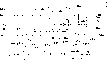
Fig. 1 is the planimetric map that the embodiment of the invention is shown.
Fig. 2 is the planimetric map that the embodiment of the invention at length is shown.
Fig. 3 is the planimetric map that illustrates in greater detail the embodiment of the invention.
Fig. 4 is the circuit structure figure that the detailed situation of sense amplifier circuit of the present invention is shown.
Fig. 5 is the planimetric map that gap portion of the present invention figure on every side is shown.
Fig. 6 is another planimetric map of the figure around the expression gap portion of the present invention.
Fig. 7 compares variation of the present invention and embodiment and the planimetric map that illustrates.
Fig. 8 is the planimetric map that the dynamic semiconductor memory device core of prior art row is shown.
Fig. 9 is the circuit structure diagram that the detailed situation of sense amplifier circuit of prior art example is shown.
Embodiment
Below, with reference to the description of drawings embodiments of the invention.
The general configuration figure of DRAM of the present invention has been shown among Fig. 1, has supposed that total memory capacity is the DRAM of 64M position.Disposing core memory piece CB0, CB1, CB2, CB3 on the semi-conductor chip 9, each core memory piece is made of the peripheral circuit of cores such as the storage unit of 16M position and attached sensor amplifier thereof, code translator.Circuit Vpp Pump takes place in the Vpp that is disposing the booster voltage Vpp that produces word line between CB0 and the CB1 and between CB2 and the CB3 respectively.The data output unit of each core memory piece CB is disposing data multiplexer circuit MUX and data buffer circuit DIB respectively.In addition, in closely being close to of each core memory piece piece, disposing the fusible link array CFUSE of the replacement data that keeps column redundancy circuits respectively.Between CB0 and CB1, dispose the reference potential generation circuit VREF of the reference potential that produces intermediate potentials such as 1/2Vcc respectively, between CB2 and CB3, disposing the electrify restoration circuit PWRON that produces the initialized initializing signal of chip internal when carrying out the power supply input.Arranged in order base potential generation circuit SSB, data input and output buffering I/O impact damper and pad (Pad), is selected between I/O data multiplexer circuit XIMUX, the CB1 of pad device and the CB3 arranged in order self-refresh control circuit Self refresh according to the data output amplitude between CB0 and the CB2, address buffer Address buffer, row system, control circuit RAS Series, data control circuit DC.In addition, the core at chip 9 is also disposing row partial decode circuit CPD, address transition detecting circuit ATD, row partial decode circuit RPD, column address on-off circuit ASD respectively.
Then, the structure of 16M pellet CB shown in Figure 2.A plurality of 32 memory cell array Cell Array and 33 sense amplifier column (core peripheral circuit) S/A Array of alternatively disposing.Constitute memory cell block, disposing array decoding circuit C/D at the one end.Along many column selection lines of column direction assortment CSL, select to drive by array decoding circuit C/D, column selection line CSL is selecting the signal supply to belong to the sense amplifier column S/AArray S/A of each row of same row.More particularly, the column selection line is used to the part activation of sense amplifier circuit and the driving of column selection gate circuit.Memory cell block is two groups up and down, constitute 16M core memory piece CB, disposing the drive signal supply circuit WDRV of the column decode circuitry corresponding (optionally driving word line WL) R/D, column decode circuitry and the RFUS-E that keeps the row redundancy circuit replacement data between the two respectively by inner row address signal with each memory cell array, in addition, also disposing data line amplifying circuit DQB, piece control circuit BC etc. respectively.In addition, also disposing respectively on the peripheral part of core memory piece CB and the corresponding P ditch of the peripheral circuit of each core type sensor amplifier driving circuit PSAD.
Shown in Fig. 3 by the structure of the folded memory cell array Cell Array of 2 sense amplifier column S/A Array.Take on each sense amplifier circuit S/A, to connect respectively the sense amplifiers shared structure of 2 pairs of bit line to BL, BL and BL ', BL ', as shown in Figure 3, become on one group the basis at per 2 sensor amplifiers and constitute memory cell array by adopting zigzag to arrange the ground assortment of Thousand Islands shape.If explain, then from the position of bit line, if according to the example that had illustrated in the prior art example, for right, left and right, left and right, left to the sensor amplifier of looking ... and if according to present embodiment, then be right, right, left, left and right, right, left, left ...Its result, at 2 bit lines to for example forming fixing gap 8 between BL0, BL0 and BL1, BL1 and the sense amplifier column S/A Array respectively.Connect the unillustrated dynamic type storage unit that constitutes by transistor and capacitor on each bit line.Among the storage unit MC, it is right to belong to connecting of same row same bit line, belongs to same word line of connecting of delegation.Word line such as above-mentioned by column decode circuitry R/D selection driving.Column decode circuitry comprises the word line driving circuit that word line is charged to " H " level by P ditch transistor npn npn at least, drives as it and uses drive signal supply circuit WDRV, uses the Vpp that produces the current potential Vpp that boosts that circuit Vpp Pump takes place as its power supply.
The detailed situation of sense amplifier circuit S/A among Fig. 3 then, has been shown among Fig. 4.The sensor amplifier that illustrated in the mass part of this sense amplifier circuit and the prior art example is consistent.Sense amplifier circuit S/A can divide into the balanced part in left side, the left side selects part, column selection door section, sensor amplifier part, right side to select part, the balanced part in right side.The balanced part in left side is by N ditch MOS transistor Q
1, Q
2And Q
3Constitute, under the control of signal S φ EQL, equilibrium is the 1/2Vcc that is supplied with by SVBL to BL1, BL1 the left side bit line.Signal S EQL wiring is made of polysilicon wire, as described later, and with MOS transistor Q
1, Q
2And Q
3Gate electrode shared, though can miniaturization but than higher resistance.In addition, SVBL wiring is made of the diffusion layer wiring, as described later and MOS transistor Q
1And Q
2Drain electrode shared, though can miniaturization but still be than higher resistance.For compensating the wiring of these high resistants, as the alternate path line, EOL, the VBL wiring that is made of metal wiring layer and S EQL, the SVBL configured in parallel that connects up, 8 zone forms the contact (i.e. shunt) of the two in the gap.The left side selects part by N ditch MOS transistor Q
4And Q
5Constitute, under the control of signal psi L, connect column selection door section and sensor amplifier part and left side bit line BL1, BL1.The column selection door section is by N ditch MOS transistor Q
6And Q
7Constitute, under the control of column selection line CSL, select to connect bit line to data line to DQ, DQ.The sensor amplifier part is by N ditch MOS transistor Q
8~Q
11And P ditch MOS transistor Q
12, Q
13Constitute, the moment that drops to OV at N ditch sensor amplifier control line SAN from 1/2Vcc is read the alignment OV direction of bit line pairs " L " side, then,, from the moment that 1/2Vcc rises to Vcc " H " side direction Vcc direction that bit line is right is read at P ditch sensor amplifier control line SAP.Particularly to by the bit line of the selected row of column selection line CSC to by MOS transistor Q
10Make it to carry out high speed and amplify action.Right side selection portion distribution is by N ditch MOS transistor Q
10And Q
15Constitute, under the control of signal R, connect column selection door section and sensor amplifier part and right side bit line BL1 ', BL1 '.The balanced part in right side is by N ditch MOS transistor Q
16, Q
17And Q
18Constitute, under the control of signal S EQR, equilibrium is the 1/2Vcc that is supplied with by SVBL to BL1 ', BL1 ' right side system bit line.Signal S EQR wiring is made of polysilicon wire, as described later and MOS transistor Q
16, Q
17And Q
18Gate electrode shared, though can miniaturization be than higher resistance.In addition, SVBL connects up as mentioned above, is made of and MOS transistor Q the diffusion layer wiring
17And Q
18Drain electrode shared, though can miniaturization but still be than higher resistance.For compensating the wiring of these high resistants,, dispose zone that the EQR, the VBL that are made of metal wiring layer be routed in gap 8 abreast with S EQR, SVBL wiring and make contact (i.e. the shunt) of the two as parallel wire.
The figure of gap 8 and periphery thereof has been shown among Fig. 5.With bit line to BL2, BL2 and bit line to the top of BL3, BL3 adjacent and by 2 pairs of bit line to equalizing circuit (the MOS transistor Q in BL1, BL1 and BL4, BL4 and the sense amplifier column
1, Q
2, Q
3Deng) in the gap 8 of institute's enclosing region, form the metal line that needs bigger zone and the contact region part 7 of polysilicon wire.In this contact portion 7, the S EQL wiring that is connected with the EQL cloth distribution that constitutes by the wide low resistance metal of 0.7 μ m (aluminium or tungsten) wiring layer and constitutes by the polysilicon wiring layer of the wide high electrical resistance of 0.35 μ m.The S EQL that is made of polysilicon wiring layer connects up and MOS transistor Q
1, Q
2And Q
3Gate electrode shared, memory cell array.Pass through, in addition, oblique line partly is a diffusion layer.Contact area 7 there is no need to be located in each gap 8, can establish 1 every a gap 8.In this case, be used for the shunt of VBL described later for the gap 8 that is available.
The figure of gap 8 and another position and periphery thereof has been shown among Fig. 6.With bit line to the end of BL6, BL6 and BL7, BL7 adjacent and by 2 pairs of bit line to the equalizing circuit (MOS in BL5, BL5 and BL8, BL8 and the sense amplifier column
*Transistor Q
1, Q
2, Q
3Deng) in the gap 8 of institute's region, the contact portion 6 that has formed the metal line that still needs bigger zone and diffusion layer region (certainly, also can be from diffusion layer region once to the polysilicon layer extraction electrode, and this polysilicon layer and metal wiring layer crossed.This situation is with identical with the situation of the illustrated mistake of Fig. 4).In this contact portion 6, the SVBL wiring that is connected with the VBL wiring that constitutes by the wide low resistance metal wiring layer of 0.7 μ m and constitutes by the diffusion layer wiring of the wide high electrical resistance of 0.35 μ m.The SVBL and the MOS transistor Q that constitute by diffusion layer
1And Q
2Drain electrode shared, memory cell array is passed through.In addition, oblique line partly is a diffusion layer.
More than show the situation of shunt in the gap 8 with Fig. 5,6.Certainly, also can be used as the shunt part of other distribution, but, then be positioned at the two ends of sense amplifier circuit S/A, so above-mentioned structure is very suitable owing to equalizing circuit if common sensor amplifier is constructed.
Like this, if use the configuration of bit line of the present invention, sensor amplifier, then because bit line is vacated fixing gap between, the sensor amplifier, so can guarantee the join domain between the signal wire.And identical with the sense amplifiers shared structure of prior art, bit line configuration is not destroyed maximum filling structures (that is, can per 2 bit lines to disposing 1 sensor amplifier).Its result can not increase chip area and realizes the low group of change of line equalizing signal etc.
The variation of the foregoing description then, is described with reference to Fig. 7.Fig. 7 (a) generally shows bit line, the sensor amplifier configuration of the foregoing description.Fig. 7 (b) is this variation.If this variation of family expenses, then identical with embodiment, connect the right sense amplifiers shared structure of 2 pairs of bit line about taking on each sense amplifier circuit S/A respectively, but not coexisting per 4 sensor amplifiers with embodiment is to pass through on one group the basis, constitutes memory cell array by the way that adopts zigzag to arrange.If explain, then from bit line to looking, the position of sensor amplifier, if according to the example that illustrated among the embodiment of front for right, right, left, left and right, right ... if and, then be right, right, right, right, left, left, left, left and right, right, right, right according to variation ...Its result, 4 bit lines to and sense amplifier column between form certain clearance respectively.The formed gap area of comparing with the foregoing description is bigger in variation.Its result, when the contact (along separate routes) that obtains between the signal wire, it is very favourable having developed into generation chip aspects such as 256M position DRAM for the miniaturization of polysilicon spacer.Also can consider that per 8 bit lines are to being one group example from Fig. 7 (b) step that readvances.
In addition, self-evident, in the scope that does not deviate from aim of the present invention, all changes can be arranged.
As discussed above, use the present invention, can provide the bit line configuration of not destroying maximum filling structures and the dynamic semiconductor memory device of having realized resistance lowerings such as line equalizing signal.
Claims (9)
1. semiconductor storage comprises:
Memory cell array, it is right that it comprises into 2N bit line of row configurations, and each bit line pair is connected with a plurality of storage unit;
It is characterized in that also comprising:
First sense amplifier array, have N first sense amplifier circuit that becomes the first row configuration in memory cell array one side, each first sense amplifier circuit and bit line to one of be connected, thereby make N of first sense amplifier array and bit line pairs to be connected;
Second sense amplifier array, have N second sense amplifier circuit that becomes the secondary series configuration at the memory cell array opposite side, another is connected each second sense amplifier circuit and bit line pairs, thereby makes the other N of second sense amplifier array and bit line pairs to be connected;
A plurality of districts, each district are positioned between one of the individual end of bit line pairs M and sensor amplifier, and wherein first signal wire and secondary signal line are in parallel in one or more districts; Wherein
First group of M, M 〉=2, adjacent bit lines is to being assigned to one of sense amplifier array, with second group of M adjacent bit lines on first group of adjacent boundary to being assigned to other sense amplifier array.
2. semiconductor storage according to claim 1 is characterized in that:
This device also so that have M bit line to and the 1st or the 2nd sense amplifier array between the zone, at this zone the 1st signal wire and the 2nd signal wire by shunt.
3. semiconductor storage according to claim 2 is characterized in that:
Wherein, each sense amplifier circuit comprises that all one has the 1st, the 2nd and the transistorized equalizing circuit of 3MOS, equalizing circuit is with an intermediate potential, balanced corresponding bit line is right, the 1st signal wire be used to control the 1st, the 2nd and the transistorized wiring of 3MOS and and gate circuit constitute an integral body, and the 2nd signal wire is the bypass wiring, is used for control signal is supplied with the 1st signal wire.
4. semiconductor storage according to claim 3 is characterized in that:
The 1st signal wire is made of polysilicon layer, and the 2nd signal wire is made of metal line.
5. semiconductor storage according to claim 2 is characterized in that:
Each sense amplifier circuit comprises 1 equalizing circuit, be used for corresponding bit line equilibrium for having intermediate potential, the 1st signal wire is the wiring that is used for intermediate potential is offered equalizing circuit, and the 2nd signal wire is the bypass wiring that is used for intermediate potential is supplied with the 1st signal wire.
6. semiconductor storage according to claim 5 is characterized in that:
The 1st signal wire is made of the diffusion of contaminants wiring, and the 2nd signal wire is made of metal line.
7. semiconductor storage according to claim 1 is characterized in that:
M is 2.
8. semiconductor storage according to claim 1 is characterized in that:
M is 4.
9. semiconductor storage according to claim 1 is characterized in that
Bit line is to recessed so that following zone is formed a space near the position of corresponding sense amplifier circuit end, and in this zone, the 1st signal wire and one article of the 2nd signal wire are by shunt and every a fixing arranged spaced sensor amplifier.
Applications Claiming Priority (2)
| Application Number | Priority Date | Filing Date | Title |
|---|---|---|---|
| JP312990/94 | 1994-12-16 | ||
| JP6312990A JPH08172169A (en) | 1994-12-16 | 1994-12-16 | Semiconductor storage device |
Publications (2)
| Publication Number | Publication Date |
|---|---|
| CN1134022A CN1134022A (en) | 1996-10-23 |
| CN1093978C true CN1093978C (en) | 2002-11-06 |
Family
ID=18035914
Family Applications (1)
| Application Number | Title | Priority Date | Filing Date |
|---|---|---|---|
| CN95120910A Expired - Lifetime CN1093978C (en) | 1994-12-16 | 1995-12-15 | Semiconductor memory storage |
Country Status (7)
| Country | Link |
|---|---|
| US (1) | US5691933A (en) |
| EP (1) | EP0717414B1 (en) |
| JP (1) | JPH08172169A (en) |
| KR (1) | KR100254069B1 (en) |
| CN (1) | CN1093978C (en) |
| DE (1) | DE69520333T2 (en) |
| TW (1) | TW295662B (en) |
Families Citing this family (24)
| Publication number | Priority date | Publication date | Assignee | Title |
|---|---|---|---|---|
| JP3291206B2 (en) * | 1996-09-17 | 2002-06-10 | 富士通株式会社 | Semiconductor storage device |
| US5771268A (en) * | 1996-12-10 | 1998-06-23 | International Business Machines Corporation | High speed rotator with array method |
| US6067655A (en) * | 1997-08-28 | 2000-05-23 | Stmicroelectronics, N.V. | Burst error limiting symbol detector system |
| US6033945A (en) * | 1998-06-03 | 2000-03-07 | G-Link Technology | Multiple equilibration circuits for a single bit line |
| JP4339938B2 (en) | 1998-06-10 | 2009-10-07 | 株式会社ルネサステクノロジ | Semiconductor memory device |
| US7157314B2 (en) | 1998-11-16 | 2007-01-02 | Sandisk Corporation | Vertically stacked field programmable nonvolatile memory and method of fabrication |
| KR100319885B1 (en) * | 1999-04-27 | 2002-01-10 | 윤종용 | Data input/output line scheme to reduce resistance of data input/output line |
| US6188596B1 (en) * | 1999-05-20 | 2001-02-13 | Advanced Micro Devices, Inc. | Layout for semiconductor memory including multi-level sensing |
| US6163495A (en) | 1999-09-17 | 2000-12-19 | Cypress Semiconductor Corp. | Architecture, method(s) and circuitry for low power memories |
| TW503396B (en) | 1999-12-03 | 2002-09-21 | Hitachi Ltd | Semiconductor device |
| US8575719B2 (en) | 2000-04-28 | 2013-11-05 | Sandisk 3D Llc | Silicon nitride antifuse for use in diode-antifuse memory arrays |
| US7184290B1 (en) * | 2000-06-28 | 2007-02-27 | Marvell International Ltd. | Logic process DRAM |
| KR100395877B1 (en) * | 2000-11-10 | 2003-08-25 | 삼성전자주식회사 | Data sensing circuit of a semiconductor memory |
| JP2003092364A (en) * | 2001-05-21 | 2003-03-28 | Mitsubishi Electric Corp | Semiconductor memory device |
| US6804145B2 (en) * | 2002-11-01 | 2004-10-12 | Hewlett-Packard Development Company, L.P. | Memory cell sensing system and method |
| CN101673754B (en) * | 2004-05-25 | 2011-11-30 | 瑞萨电子株式会社 | Semiconductor device |
| US7327591B2 (en) * | 2004-06-17 | 2008-02-05 | Texas Instruments Incorporated | Staggered memory cell array |
| US7218564B2 (en) * | 2004-07-16 | 2007-05-15 | Promos Technologies Inc. | Dual equalization devices for long data line pairs |
| JP4400497B2 (en) * | 2005-03-31 | 2010-01-20 | エルピーダメモリ株式会社 | Semiconductor memory device |
| JP4989900B2 (en) * | 2006-01-31 | 2012-08-01 | ルネサスエレクトロニクス株式会社 | Parallel processing unit |
| JP4428384B2 (en) | 2006-12-25 | 2010-03-10 | エルピーダメモリ株式会社 | Semiconductor memory device |
| FR2972838B1 (en) | 2011-03-18 | 2013-04-12 | Soitec Silicon On Insulator | SEMICONDUCTOR MEMORY HAVING DECAL READING AMPLIFIERS ASSOCIATED WITH A LOCAL COLUMN DECODER |
| WO2014112472A1 (en) * | 2013-01-15 | 2014-07-24 | ピーエスフォー ルクスコ エスエイアールエル | Semiconductor device |
| CN113129941A (en) * | 2019-12-31 | 2021-07-16 | 福建省晋华集成电路有限公司 | Semiconductor memory device |
Citations (1)
| Publication number | Priority date | Publication date | Assignee | Title |
|---|---|---|---|---|
| US5280448A (en) * | 1987-11-18 | 1994-01-18 | Sony Corporation | Dynamic memory with group bit lines and associated bit line group selector |
Family Cites Families (7)
| Publication number | Priority date | Publication date | Assignee | Title |
|---|---|---|---|---|
| JPS5683891A (en) * | 1979-12-13 | 1981-07-08 | Fujitsu Ltd | Semiconductor storage device |
| JPH07107797B2 (en) * | 1987-02-10 | 1995-11-15 | 三菱電機株式会社 | Dynamic random access memory |
| JPS6413290A (en) * | 1987-07-07 | 1989-01-18 | Oki Electric Ind Co Ltd | Semiconductor memory |
| JP2691280B2 (en) * | 1988-05-12 | 1997-12-17 | 三菱電機株式会社 | Semiconductor memory device |
| EP0496406B1 (en) * | 1991-01-25 | 1999-05-06 | Nec Corporation | Semiconductor memory apparatus |
| KR100292170B1 (en) * | 1991-06-25 | 2001-06-01 | 사와무라 시코 | Semiconductor memory device |
| JP2945216B2 (en) * | 1992-09-17 | 1999-09-06 | シャープ株式会社 | Semiconductor memory device |
-
1994
- 1994-12-16 JP JP6312990A patent/JPH08172169A/en active Pending
-
1995
- 1995-10-13 DE DE69520333T patent/DE69520333T2/en not_active Expired - Lifetime
- 1995-10-13 EP EP95116185A patent/EP0717414B1/en not_active Expired - Lifetime
- 1995-12-15 CN CN95120910A patent/CN1093978C/en not_active Expired - Lifetime
- 1995-12-15 KR KR1019950050395A patent/KR100254069B1/en not_active IP Right Cessation
-
1996
- 1996-02-01 TW TW085101269A patent/TW295662B/zh not_active IP Right Cessation
- 1996-12-18 US US08/769,185 patent/US5691933A/en not_active Expired - Lifetime
Patent Citations (1)
| Publication number | Priority date | Publication date | Assignee | Title |
|---|---|---|---|---|
| US5280448A (en) * | 1987-11-18 | 1994-01-18 | Sony Corporation | Dynamic memory with group bit lines and associated bit line group selector |
Also Published As
| Publication number | Publication date |
|---|---|
| EP0717414A2 (en) | 1996-06-19 |
| KR960025729A (en) | 1996-07-20 |
| TW295662B (en) | 1997-01-11 |
| KR100254069B1 (en) | 2000-04-15 |
| DE69520333T2 (en) | 2001-08-09 |
| DE69520333D1 (en) | 2001-04-19 |
| EP0717414B1 (en) | 2001-03-14 |
| JPH08172169A (en) | 1996-07-02 |
| EP0717414A3 (en) | 1996-11-06 |
| US5691933A (en) | 1997-11-25 |
| CN1134022A (en) | 1996-10-23 |
Similar Documents
| Publication | Publication Date | Title |
|---|---|---|
| CN1093978C (en) | Semiconductor memory storage | |
| TW459379B (en) | Semiconductor memory device | |
| JP4427847B2 (en) | Dynamic RAM and semiconductor device | |
| JP4044401B2 (en) | Semiconductor memory device | |
| KR101156172B1 (en) | Semiconductor integrated circuit device | |
| KR100714300B1 (en) | Semiconductor device | |
| US7161823B2 (en) | Semiconductor memory device and method of arranging signal and power lines thereof | |
| US8218386B2 (en) | Embedded memory databus architecture | |
| JP3753331B2 (en) | Ferroelectric memory device | |
| TW594977B (en) | Semiconductor integrated circuit device | |
| CN1213834A (en) | High density semiconductor memory having diagonal bit lines and dual word lines | |
| CN1084516C (en) | Semi-conductor memory | |
| KR920001328B1 (en) | Dram having open bit line structure | |
| US6097623A (en) | Ferroelectric memory device having two columns of memory cells precharged to separate voltages | |
| CN1145969C (en) | Interleaved sense amplifier with single-sided precharge device | |
| CN100424877C (en) | Semiconductor memory device and method of arranging signal and power lines thereof | |
| US6545902B2 (en) | Ferroelectric memory device | |
| US6930908B2 (en) | Semiconductor integrated circuit device having ferroelectric capacitor | |
| KR100231404B1 (en) | Small-sized multi-valued semiconductor memory device | |
| TW421742B (en) | Semiconductor memory apparatus | |
| KR100231685B1 (en) | Semiconductor memory device | |
| US5933380A (en) | Semiconductor memory device having a multilayered bitline structure with respective wiring layers for reading and writing data | |
| JP4949451B2 (en) | Dynamic RAM and semiconductor device | |
| CN1568523A (en) | Sense amplifier and architecture for open digit arrays | |
| CN1339158A (en) | Integrated memory and corresponding operating method |
Legal Events
| Date | Code | Title | Description |
|---|---|---|---|
| C10 | Entry into substantive examination | ||
| SE01 | Entry into force of request for substantive examination | ||
| C06 | Publication | ||
| PB01 | Publication | ||
| C14 | Grant of patent or utility model | ||
| GR01 | Patent grant | ||
| CX01 | Expiry of patent term |
Granted publication date: 20021106 |
|
| EXPY | Termination of patent right or utility model |