CN108337459B - Image pickup apparatus and image pickup system - Google Patents
Image pickup apparatus and image pickup system Download PDFInfo
- Publication number
- CN108337459B CN108337459B CN201810153221.0A CN201810153221A CN108337459B CN 108337459 B CN108337459 B CN 108337459B CN 201810153221 A CN201810153221 A CN 201810153221A CN 108337459 B CN108337459 B CN 108337459B
- Authority
- CN
- China
- Prior art keywords
- period
- image pickup
- pixels
- electric charges
- photoelectric conversion
- Prior art date
- Legal status (The legal status is an assumption and is not a legal conclusion. Google has not performed a legal analysis and makes no representation as to the accuracy of the status listed.)
- Active
Links
Images


Classifications
-
- H—ELECTRICITY
- H04—ELECTRIC COMMUNICATION TECHNIQUE
- H04N—PICTORIAL COMMUNICATION, e.g. TELEVISION
- H04N23/00—Cameras or camera modules comprising electronic image sensors; Control thereof
- H04N23/70—Circuitry for compensating brightness variation in the scene
- H04N23/73—Circuitry for compensating brightness variation in the scene by influencing the exposure time
-
- H—ELECTRICITY
- H04—ELECTRIC COMMUNICATION TECHNIQUE
- H04N—PICTORIAL COMMUNICATION, e.g. TELEVISION
- H04N25/00—Circuitry of solid-state image sensors [SSIS]; Control thereof
- H04N25/50—Control of the SSIS exposure
- H04N25/53—Control of the integration time
-
- H—ELECTRICITY
- H04—ELECTRIC COMMUNICATION TECHNIQUE
- H04N—PICTORIAL COMMUNICATION, e.g. TELEVISION
- H04N25/00—Circuitry of solid-state image sensors [SSIS]; Control thereof
- H04N25/50—Control of the SSIS exposure
- H04N25/53—Control of the integration time
- H04N25/531—Control of the integration time by controlling rolling shutters in CMOS SSIS
-
- H—ELECTRICITY
- H04—ELECTRIC COMMUNICATION TECHNIQUE
- H04N—PICTORIAL COMMUNICATION, e.g. TELEVISION
- H04N25/00—Circuitry of solid-state image sensors [SSIS]; Control thereof
- H04N25/70—SSIS architectures; Circuits associated therewith
- H04N25/71—Charge-coupled device [CCD] sensors; Charge-transfer registers specially adapted for CCD sensors
- H04N25/75—Circuitry for providing, modifying or processing image signals from the pixel array
-
- H—ELECTRICITY
- H04—ELECTRIC COMMUNICATION TECHNIQUE
- H04N—PICTORIAL COMMUNICATION, e.g. TELEVISION
- H04N25/00—Circuitry of solid-state image sensors [SSIS]; Control thereof
- H04N25/70—SSIS architectures; Circuits associated therewith
- H04N25/76—Addressed sensors, e.g. MOS or CMOS sensors
-
- H—ELECTRICITY
- H04—ELECTRIC COMMUNICATION TECHNIQUE
- H04N—PICTORIAL COMMUNICATION, e.g. TELEVISION
- H04N25/00—Circuitry of solid-state image sensors [SSIS]; Control thereof
- H04N25/70—SSIS architectures; Circuits associated therewith
- H04N25/76—Addressed sensors, e.g. MOS or CMOS sensors
- H04N25/77—Pixel circuitry, e.g. memories, A/D converters, pixel amplifiers, shared circuits or shared components
- H04N25/771—Pixel circuitry, e.g. memories, A/D converters, pixel amplifiers, shared circuits or shared components comprising storage means other than floating diffusion
Abstract
The invention relates to an image pickup apparatus and an image pickup system. The image pickup apparatus performs a global electronic shutter action in which exposure periods of a plurality of pixels coincide with each other. In a first period in which the photoelectric conversion unit of at least one of the pixels stores electric charges, signals based on the electric charges stored in the holding units of the pixels are sequentially output to the output lines. In a second period after the termination of the output of the signal from the pixel, the holding unit of the pixel holds the charge.
Description
The present application is a divisional application of the chinese patent application with an application date of 2015, 3/13, and an application number of 201510110188.X, entitled "image pickup apparatus and image pickup system".
Technical Field
The present disclosure relates to an image pickup apparatus and an image pickup system.
Background
In recent years, it has been proposed to use a global electronic shutter in a CMOS image sensor. The image pickup devices disclosed in japanese patent laid-open nos. 2004-111590 and 2006-246450 have such an advantage: even when an image of a rapidly moving subject is captured, the subject image is not distorted.
Disclosure of Invention
According to an aspect of the present disclosure, an image pickup apparatus includes a plurality of pixels. Each pixel includes a photoelectric conversion unit configured to generate electric charges in response to incident light and accumulate the electric charges, a holding unit configured to hold the electric charges, an amplification unit configured to output a signal based on the electric charges, a first transfer switch configured to transfer the electric charges from the photoelectric conversion unit to the holding unit, and a second transfer switch configured to transfer the electric charges from the holding unit to the amplification unit. The image pickup apparatus includes an output line to which signals from a plurality of pixels are output. At a first point in time, the photoelectric conversion units of the plurality of pixels start accumulation of electric charges. The first transfer switch of at least one of the plurality of pixels is kept off from a first time point to a second time point, and the photoelectric conversion unit of at least one of the plurality of pixels accumulates electric charges generated in a first period from the first time point to the second time point. In the first period, the second transfer switches of the plurality of pixels are turned on, and the amplifying units of the plurality of pixels output signals to the output lines. In a second period from the second point to the third point, the holding units of the plurality of pixels hold the electric charges generated by the photoelectric conversion units in the first period and the electric charges generated by the photoelectric conversion units in the second period. At a third point in time, the first transfer switches of the plurality of pixels are controlled from on to off.
According to an aspect of the present disclosure, an image pickup apparatus includes a plurality of pixels. Each pixel includes a photoelectric conversion unit configured to generate charges in response to incident light and accumulate the charges, a holding unit configured to hold the charges in a portion different from the photoelectric conversion unit, and an amplification unit configured to output a signal based on the charges. The image pickup apparatus includes an output line to which signals from a plurality of pixels are output. The electric charges generated in the first period are accumulated in the photoelectric conversion units of the plurality of pixels. The holding units of the plurality of pixels hold the electric charges generated by the photoelectric conversion units in the first period and the electric charges generated by the photoelectric conversion units in the second period during a second period subsequent to the first period. In each of the plurality of pixels, the electric charge held by the holding unit is read to the amplifying unit in the first period.
Other features of the present disclosure will become apparent from the following description of exemplary embodiments with reference to the attached drawings.
Drawings
Fig. 1 is a diagram illustrating an equivalent circuit of an image pickup apparatus.
Fig. 2 is a diagram schematically showing a sectional structure of the image pickup apparatus.
Fig. 3 is a diagram illustrating a driving pulse of the image pickup apparatus.
Fig. 4 is a diagram illustrating a driving pulse of the image pickup apparatus.
Fig. 5 is a diagram schematically showing the action of the image pickup apparatus.
Fig. 6 is a diagram schematically showing a sectional structure of an image pickup apparatus.
Fig. 7 is a diagram illustrating an equivalent circuit of the image pickup apparatus.
Fig. 8 is a diagram schematically showing a sectional structure of the image pickup apparatus.
Fig. 9A and 9B are diagrams illustrating driving pulses of the image pickup apparatus.
Fig. 10 is a diagram schematically showing a sectional structure of an image pickup apparatus.
Fig. 11 is a diagram schematically showing a sectional structure of an image pickup apparatus.
Fig. 12 is a diagram illustrating a driving pulse of the image pickup apparatus.
Fig. 13 is a block diagram showing the configuration of the image pickup system.
Detailed Description
According to the following embodiments, the global electronic shutter can be operated while the saturated charge amount or the saturated charge amount can be improved.
In the image pickup apparatus disclosed in japanese patent laid-open No.2004-111590, all the electric charges generated by photoelectric conversion for obtaining one image or one frame are accumulated in the photoelectric conversion unit. Then, the charges in all the pixels are simultaneously transferred from the photoelectric conversion unit to the holding unit, and photoelectric conversion is started to obtain the next image or the next frame. Therefore, in order to increase the saturation charge amount of the pixel, the saturation charge amount of the photoelectric conversion unit and the saturation charge amount of the holding unit are substantially the same. When the saturation charge amount of the photoelectric conversion unit increases, the area of the photoelectric conversion unit increases. Therefore, the size of the pixel may increase.
In the image pickup device disclosed in japanese patent laid-open No.2006-246450, the photoelectric conversion unit does not accumulate electric charges, but the holding unit stores almost all of the electric charges. Therefore, the saturation charge amount of the pixel can be increased without increasing the saturation charge amount of the photoelectric conversion unit. However, there is a period in this method in which the generated electric charges are not allowed to be stored, and therefore, the image quality may be deteriorated.
The inventors found that in some image pickup apparatuses, it is difficult to increase the saturation charge amount of the pixel. According to some embodiments described herein, in an image pickup apparatus using a global electronic shutter, the saturation charge amount of a pixel can be increased.
The embodiment provides an image pickup apparatus including a plurality of pixels and output lines to which signals are supplied from the plurality of pixels. Each of the pixels includes a photoelectric conversion unit, a holding unit that holds electric charges, and an amplification unit that outputs a signal based on the electric charges. Each of the pixels further includes a first transfer switch that transfers electric charge from the photoelectric conversion unit to the holding unit and a second transfer switch that transfers electric charge from the holding unit to the amplifying unit. With this configuration, an image pickup action in which photoelectric conversion periods coincide, so-called "global electronic shutter", can be performed. An electronic shutter is defined, for example, to electrically control the accumulation of charge generated in response to incident light. A transfer switch (or transistor) and/or a discharge switch (or transistor) may be used to define the period of accumulation.
In the embodiments of the present disclosure, the photoelectric conversion units of the pixels simultaneously start accumulation or storage of electric charges at the first time point. The first transfer switch of at least one of the pixels remains off from the first point in time to or until the second point in time. In the at least one of the pixels, the electric charges generated in the period are accumulated or stored in the photoelectric conversion unit. A period from the first time point to the second time point corresponds to the first period. In other words, the first period may be defined as starting at a first time and ending at a second time.
In the first period, the output unit of the pixel sequentially or continuously outputs a signal based on the electric charges held in the holding unit of the pixel to the output line. In other words, each of the pixels outputs at least one signal in the first period. Specifically, the first transfer switches of the pixels are sequentially turned on in the first period. Since the electric charges generated in the first period are accumulated in the photoelectric conversion unit, the holding unit can hold the electric charges generated before the first time point in the first period.
The number of signals output in the first period may vary according to the format of an image to be output. In the case of shooting a moving image, for example, it suffices to output signals of the number corresponding to the number of horizontal lines for one frame. In such an embodiment, it is not necessarily the case that all pixels included in the image pickup device output signals.
After the signal is output from the pixel, the holding unit of the pixel holds or stores the electric charge at least in a second period from the second time point to a third time point. The second period of time may be defined as beginning at a second time and ending at a third time. In the second period, the holding unit holds the electric charges generated in the first period and the electric charges generated in the second period. At a third point in time, the first transfer switches of the pixels are simultaneously controlled from the on-state to the off-state. In other words, at the third point in time, the first transfer switches of the pixels are simultaneously controlled from on to off.
Since the photoelectric conversion unit stores at least the electric charges generated in the first period, even if the saturation charge amount of the photoelectric conversion unit is small, the saturation charge amount of the pixel can be maintained or even increased. Therefore, with this configuration, the global electronic shutter can be operated while the saturation charge amount is maintained. Note that in some embodiments, the second period during which the holding unit of the pixel holds the charge is longer than the first period. This is because, in the case where the second period is longer than the first period, the saturation charge amount of the photoelectric conversion unit can be reduced.
Embodiments of the present disclosure will be described below with reference to the accompanying drawings. Embodiments of the present disclosure are not limited to the embodiments described below. For example, in the embodiment of the present disclosure, an embodiment in which a part of the constitution of one of the following embodiments is added to one of the other embodiments and an embodiment in which a part of the constitution of one of the following embodiments is replaced with a part of one of the other embodiments are also included. Also, in the following embodiments, the first conductive type is an N-type and the second conductive type is a P-type. However, the first conductive type may be a P type and the second conductive type may be an N type.
First embodiment
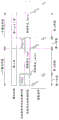
The first embodiment will be described. Fig. 1 is a diagram illustrating an equivalent circuit of a pixel of an image pickup apparatus. Although four pixels 20 are illustrated in fig. 1, the image pickup apparatus includes more pixels.
Each of the pixels 20 includes a photoelectric conversion unit 1, a holding unit 2, an amplification unit 10, a first transfer switch 4, and a second transfer switch 5. Each of the pixels 20 further includes a reset transistor 9 and a selection transistor 7.
The photoelectric conversion unit 1 generates charges in response to incident light. The photoelectric conversion unit 1 accumulates or stores electric charges generated in response to incident light. The first transfer switch 4 transfers the charge of the photoelectric conversion unit 1 to the holding unit 2. The holding unit 2 holds the charge generated by incident light in a portion other than the photoelectric conversion unit 1. The second transfer switch 5 transfers the charge of the holding unit 2 to the input node 3 of the amplifying unit 10. The reset transistor 9 resets the voltage of the input node 3 of the amplifying unit 10. The selection transistor 7 selects a corresponding one of the pixels 20 that output signals to the output line 8. The amplification unit 10 outputs a signal based on the electric charge generated by the incident light to the output line 8. The amplification unit 10 is, for example, a source follower. Also, the first transfer switch 4 and the second transfer switch 5 are MOS transistors.
The control line Tx1 is connected to the first transfer switch 4. The control line Tx2 is connected to the second transfer switch 5. In the present embodiment, a plurality of pixels are arranged in a matrix. The common control line is connected to the pixels in the same row. Therefore, the control line Tx1(n) is connected to the pixels in the nth row.
With this configuration, the electric charges generated while the holding unit 2 holds the electric charges can be stored in the photoelectric conversion unit 1. Therefore, an image pickup action in which the periods of time during which photoelectric conversion is performed in the pixels match each other, so-called "global electronic shutter", can be performed.
Fig. 2 is a diagram schematically showing a sectional structure of the image pickup apparatus. In fig. 2, a cross section of one of the pixels 20 is shown. Portions having the same functions as those of the portions in fig. 1 are denoted by the same reference numerals as those of fig. 1. Although the surface illumination type image pickup device is illustrated in fig. 2, a rear surface illumination type image pickup device may be used.
The photoelectric conversion unit 1 has an embedded photodiode structure. The photoelectric conversion unit 1 includes an N-type semiconductor region 11 and a P-type semiconductor region 12. The N-type semiconductor region 11 and the P-type semiconductor region 12 form a PN junction. The P-type semiconductor region 12 enables suppression of noise at the interface.
The P-type semiconductor region 14 is a well. An N-type semiconductor region 13 is disposed below the N-type semiconductor region 11. The N-type semiconductor region 13 has an impurity concentration lower than that of the N-type semiconductor region 11. Therefore, the electric charges generated in the deep portion are collected in the N-type semiconductor region 11. Here, the N-type semiconductor region 13 may be a P-type semiconductor region 13. A P-type semiconductor region 17 serving as a barrier for charges is provided below the N-type semiconductor region 13.
The holding unit 2 includes an N-type semiconductor region 201. The N-type semiconductor region 201 holds an electric charge corresponding to a signal. The N-type semiconductor region 201 has an impurity concentration higher than that of the N-type semiconductor region 11.
The gate electrode 40 constitutes a gate of the first transfer switch 4. And, the gate electrode 50 constitutes a gate of the second transfer switch 5. A part of the gate electrode 40 overlaps with the N-type semiconductor region 201 through the gate insulating film. Holes can be introduced on the surface of the N-type semiconductor region 201 by applying a negative voltage to the gate electrode 40. Thus, noise generated in the interface can be suppressed.
The light directed to the holding unit 2 is blocked by the light blocking unit 203. The light blocking unit 203 is formed of a metal such as tungsten or aluminum through which visible light hardly passes. The color filter 100 and the microlens 101 are disposed on the opening of the light shielding unit 203.
The photoelectric conversion unit 1 and the holding unit 2 are provided on a semiconductor substrate. In the present embodiment, the area of orthogonal projection of the photoelectric conversion unit 1 on the surface parallel to the surface of the semiconductor substrate is smaller than the area of orthogonal projection of the holding unit 2 on the same surface. With this configuration, the saturation charge amount of the pixel can be effectively increased while noise reduction is achieved.
In order to increase the saturation charge amount of the pixel, the holding unit 2 preferably has a large saturation charge amount. When the impurity concentration of the N-type semiconductor region 201 in the holding unit 2 is increased or the area of the N-type semiconductor region 201 is increased in a plan view, the saturation charge amount of the holding unit 2 can be increased. However, when the impurity concentration of the N-type semiconductor region 201 is high, leakage current or the like may be large and thus noise may be increased. Therefore, the saturation charge amount can be increased by increasing the area of the N-type semiconductor region 201 in a plan view while suppressing the impurity concentration of the N-type semiconductor region 201.
As described above, when the area of the holding unit 2 in a plan view, that is, the area of the orthogonal projection of the holding unit 2 is increased, the saturation charge amount of the pixel can be increased while reducing noise. In this case, the area of the photoelectric conversion unit 1 may be relatively small in a plan view, and it is difficult to increase the saturation charge amount of the photoelectric conversion unit 1. Therefore, even if the saturation charge amount of the photoelectric conversion unit 1 is small, the saturation charge amount of the pixel is more effectively maintained.
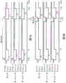
A driving method of the image pickup apparatus of the present embodiment will be described. Fig. 3 is a diagram schematically showing the drive pulse according to the present embodiment. In fig. 3, the respective driving pulses supplied to the control line Tx1 of the first transfer switch 4 and the control line Tx2 of the second transfer switch 5 of the pixels in the nth to (n +2) th rows are shown. When the drive pulse is at a high level, the corresponding transistor or the corresponding switch is turned on. When the drive pulse is at a low level, the corresponding transistor or the corresponding switch is turned off. These driving pulses are supplied by a control unit included in the image pickup apparatus. As the control unit, a logic circuit such as a shift register or an address decoder is used.
First, before a time point T1, the previous frame is exposed. The term "exposure" means that electric charges generated by photoelectric conversion are stored or held as signals. The electric charge generated before the time point T1 is held by the holding unit 2. When the first transfer switches 4 of all the pixels that supply electric charges from the photoelectric conversion unit 1 to the holding unit 2 are simultaneously turned off, the exposure of the previous frame is terminated (at a time point T1 of fig. 1).
Also, at a time point T1, all the electric charges of the photoelectric conversion unit 1 are transferred to the holding unit 2. That is, the photoelectric conversion unit 1 enters the initial state. Therefore, at the time point T1, the photoelectric conversion units 1 of the pixels in the three rows simultaneously start storage of electric charges. In this way, in the present embodiment, the charge storage by the photoelectric conversion unit 1 is started at the time of turning off the first transfer switch 4.
In the first period from the time point T1 to the time point T2, the off state of the first transfer switch 4 is maintained. In the present embodiment, the off state of the first transfer switches 4 of all the pixels is maintained. However, it is sufficient that the off state of the first transfer switch 4 of at least one of the pixels is maintained in the period from the time point T1 to the time point T2.
When the first period elapses after the time point T1, a time point T2 is reached. Specifically, the first period corresponds to a period from a time point T1 to a time point T2. In the first period, the electric charges generated in the first period are stored in the photoelectric conversion unit 1. Meanwhile, the holding unit 2 holds the electric charge generated in the previous frame in the first period.
In the first period, the charges in the holding unit 2 are sequentially read to the input node 3 of the amplifying unit 10. Specifically, when the second transfer switch 5 in the nth row is turned on, the electric charges of the holding units 2 of the pixels in the nth row are transferred to the input node 3. The voltage of the input node 3 changes according to the capacitance of the input node 3 and the amount of transferred charge. The amplifying unit 10 outputs a signal based on the voltage of the input node 3 to the output line 8. Then, the same action is performed on the pixels in the (n +1) th row. This action is performed from the pixels on the first row to the pixels in the last row. After reading is performed on the last pixel, the first transfer switches 4 and the second transfer switches 5 of all pixels are in the off state.
At a time point T2, the first transfer switch 4 is turned on. Thus, the electric charges of the photoelectric conversion unit 1 are transferred to the holding unit 2. Specifically, the electric charge generated in the first period is held by the holding unit 2 after the time point T2. In the present embodiment, the off-states of the first transfer switches 4 of all the pixels are simultaneously changed to the on-states. However, it is sufficient that the first transfer switches 4 of the pixels are in the on state before the time point T2, and the timings of the changes may be shifted from each other. For example, the first transfer switches 4 of the pixels subjected to the above-described reading action may be sequentially turned on.
Then, in a second period from a time point T2 to a time point T3, the holding unit 2 holds the electric charge generated in the first period and the electric charge generated in the second period. In the present embodiment, the on state of the first transfer switch 4 is maintained in the second period. Therefore, the electric charges generated in the second period are immediately transferred to the holding unit 2. Note that the period of time for transferring electric charges from the photoelectric conversion unit 1 to the holding unit 2 can be arbitrarily set. In a part of the second period, the first transfer switch 4 may be in an off state.
At a time point T3, the on states of the first transfer switches 4 of the pixels in all the rows simultaneously become the off states. Thus, the exposure period of one frame is terminated. As described above, the exposure periods of all the pixels match each other. Specifically, in all pixels, exposure is started at a time point T1 and terminated at a time point T3. Also, exposure of the next frame is started at a time point T3, and then, the action from the time point T1 to the time point T3 is repeatedly performed.
Fig. 4 is a diagram schematically showing a driving pulse used in the image pickup apparatus, and in fig. 4, a driving pulse SE L supplied to the selection transistor 7, a driving pulse RES supplied to the reset transistor 9, and a driving pulse tx2 supplied to the second transfer switch 5 are shown.
According to the driving pulse shown in fig. 4, selection of a pixel, reset, reading of a noise signal (N reading), transfer of electric charge, and reading of an optical signal (S reading) are performed. The output signal may be subjected to AD conversion outside the image pickup apparatus. The AD conversion may be performed inside the image pickup apparatus.
The effects of the present embodiment will be described below. Fig. 5 is a diagram schematically showing the action of the image pickup apparatus. In fig. 5, the image pickup action performed on the nth frame to the (n +1) th frame is shown. The action performed on the nth frame is indicated by a solid line, and the action performed on the (n +1) th frame is indicated by a dotted line.
In fig. 5, an exposure period of a frame, a period during which the photoelectric conversion unit 1 stores electric charges, and a period during which the holding unit 2 holds electric charges are illustrated. According to fig. 5, a reading action is performed on a plurality of pixels in a first period. The reading action in fig. 5 includes the charge transfer using the second transfer switch 5 and the signal output performed by the amplifying unit 10 described with reference to fig. 3 and 4.
As shown in fig. 5, immediately after the exposure for one frame is terminated, the next exposure may be started. In this way, the period of lacking information is substantially eliminated, and thus the image quality can be improved.
Also, as shown in fig. 5, a reading action is individually performed on the pixels during the first period in which the photoelectric conversion unit 1 stores electric charges. Therefore, even when the saturation charge amount of the photoelectric conversion unit 1 is small, the saturation charge amount of the pixel can be increased. The saturation charge amount of the pixel corresponds to the maximum value of the charge amount serving as a signal among the charges generated in one exposure or a single frame. The saturation charge amount of the photoelectric conversion unit 1 corresponds to the maximum value of the amount of charge allowed to be stored in the photoelectric conversion unit 1. The saturated charge amount of the holding unit 2 corresponds to the maximum value of the amount of charge allowed to be stored in the holding unit 2.
One exposure period is obtained as the sum of the first period and the second period. Here, the electric charges of the previous frame held in the holding unit 2 are read in the first period. Therefore, the holding unit 2 can hold the electric charge after the first period. Therefore, it is sufficient for the photoelectric conversion unit 1 to store at least the electric charges generated in the first period. In general, the amount of electric charges generated in the first period is smaller than the amount of electric charges generated in one exposure period, and thus the saturation charge amount of the photoelectric conversion unit 1 can be reduced.
As shown in fig. 5, in the present embodiment, the second period during which the holding unit 2 holds the electric charges is longer than the first period. Therefore, the saturation charge amount of the photoelectric conversion unit 1 can be further reduced. However, the first period may be equal to the second period, or the first period may be longer than the second period.
In fig. 5, a case where the reading action is performed sequentially from the first row is explained as an example. However, the order of the read actions is not limited to this example. The reading action is performed at least once on each of the pixels included in one frame in the first period. Also, in at least some of the pixels, a period of time from when the holding unit 2 starts holding of electric charge in a certain frame to when the holding unit 2 starts holding of electric charge in the next frame is equal to the exposure time.
It is preferable that the ratio of the sum of the first period and the second period to the first period is substantially equal to the ratio of the saturated charge amount of the holding unit 2 to the saturated charge amount of the photoelectric conversion unit 1. Here, the sum of the first period and the second period corresponds to one exposure period.
In the present embodiment, the ratio of one exposure period to the first period is 4: 1. That is, the first period corresponds to one quarter of one exposure period. In the case where a moving image of 60 frames per second is to be captured, for example, the first period corresponds to 1/240 seconds.
Therefore, it is preferable that the ratio of the saturation charge amount of the holding unit 2 to the saturation charge amount of the photoelectric conversion unit 1 is close to 4: 1. This is because, although the holding unit 2 holds all the electric charges generated in one exposure period, the photoelectric conversion unit 1 holds at least one-fourth of the electric charges. This ratio of the saturation charge amount enables optimization of the sizes of the photoelectric conversion unit 1 and the holding unit 2.
Note that the image pickup apparatus of the present embodiment may have an action mode for executing a rolling shutter. In the operation mode for the rolling shutter, the photoelectric conversion units 1 of the pixels sequentially start storage of electric charges. Then, the first transfer switches 4 of the pixels are sequentially turned on. The image pickup apparatus of the present embodiment may also have an action mode for a global electronic shutter using another method. An example of the global electronic shutter using another method includes an action in which the time period during which the photoelectric conversion unit 1 stores electric charges becomes equal to the exposure period.
As described above, according to the image pickup apparatus of the present embodiment, the global electronic shutter can be operated while increasing the saturation charge amount.
Second embodiment
A second embodiment will be described. In the present embodiment, the configuration of the holding unit is different from that of the first embodiment. Therefore, only portions different from the first embodiment are described, and description of portions identical to the first embodiment is omitted.
The equivalent circuit of this embodiment is the same as that of the first embodiment. Specifically, fig. 1 is a diagram showing an equivalent circuit of a pixel of the image pickup apparatus of the present embodiment. Since the description of fig. 1 is the same as that of the first embodiment, the description is omitted here.
The driving method of this embodiment is the same as that of the first embodiment. Specifically, fig. 3 and 4 are diagrams schematically showing the driving pulses according to the present embodiment. Also, fig. 5 is a diagram schematically showing the action of the image pickup apparatus of the present embodiment. Since the description of fig. 3 to 5 is the same as that of the first embodiment, the description is omitted here.
Fig. 6 is a diagram schematically showing a sectional structure of an image pickup apparatus. In fig. 6, a cross section of a pixel is shown. The portions having the same functions as those in FIGS. 1 to 5 are denoted by the same reference numerals as those in FIGS. 1 to 5.
The holding unit 2 includes an N-type semiconductor region 201 and a P-type semiconductor region 202. The P-type semiconductor region 202 is disposed on the N-type semiconductor region 201. The P-type semiconductor region 202 enables suppression of noise at the interface.
Also, the gate electrode 40 of the first transfer switch 4 does not extend on the N-type semiconductor region 201. Therefore, the limitation of the layout is reduced, and thus the degree of freedom of design can be improved.
As described above, according to the present embodiment, in addition to the effects of the first embodiment, noise can be reduced.
Third embodiment
A third embodiment will be described. The present embodiment is different from the first and second embodiments in that the pixel has a discharge switch. Therefore, only portions different from the first and second embodiments are described, and description of portions identical to those of the first and second embodiments is omitted.
Fig. 7 is a diagram illustrating an equivalent circuit of a pixel of the image pickup device. The same portions as those of fig. 1 are denoted by the same reference numerals as those of fig. 1. Note that, in order to simplify the drawing, reference numerals of the control lines Tx1 and Tx2 are omitted. The control lines Tx1 and Tx2 have the same configuration as in the first embodiment.
Each of the pixels has a discharge switch 18. The discharge switch 18 discharges the electric charges of the photoelectric conversion unit 1 to a power supply node such as an overflow drain (overflow drain). The control line OFG is connected to the discharge switch 18. The discharge switch 18 is, for example, a MOS transistor.
In the first embodiment, the storage of electric charges in the photoelectric conversion unit 1 is started by changing the state of the second transfer switch 5 from the on state to the off state. In the present embodiment, as shown in fig. 9A and 9B, the start of exposure can be controlled by controlling the discharge switch 18. Specifically, by changing the state of the discharge switch 18 from the on state to the off state, the storage of electric charges in the photoelectric conversion unit 1 is started. Thus, the exposure period can be set arbitrarily.
Fig. 8 is a diagram schematically showing a sectional structure of the image pickup apparatus. Portions having the same functions as those of fig. 1 and 2 are denoted by the same reference numerals as those of fig. 1 and 2. Fig. 8 is a diagram showing a case where the holding unit 2 includes the P-type semiconductor region 202 as an example, as in the second embodiment. As shown in fig. 1, the holding unit 2 may not include the P-type semiconductor region 202.
The discharge switch 18 includes an overflow control electrode 16 and an overflow drain 15. The electric charges of the photoelectric conversion unit 1 are discharged to the overflow drain 15 according to the voltage supplied to the overflow control electrode 16. A predetermined voltage is supplied to the overflow drain 15. The light directed to the overflow control electrode 16 and the overflow drain 15 is blocked by the light shielding unit 203.
A driving method of the image pickup apparatus of the present embodiment will be described. Fig. 9A and 9B are diagrams schematically showing drive pulses according to the present embodiment. In fig. 9A and 9B, the driving pulses supplied to the control lines Tx1 and Tx2 and the control line OFG in the nth to (n +2) th rows are illustrated. The driving pulses supplied to the control lines Tx1 and Tx2 are the same as those of the first embodiment.
When the drive pulse is at a high level, the corresponding transistor or the corresponding switch is turned on. When the drive pulse is at a low level, the corresponding transistor or the corresponding switch is turned off. These driving pulses are supplied by a control unit included in the image pickup apparatus. A logic circuit such as a shift register or an address decoder is used as a control unit.
The timing of the operation of the discharge switch 18 in fig. 9A and 9B is the same and different. In fig. 9A, the state of the discharge switch 18 changes from the on state to the off state at a time point T4. When the discharge switch 18 is in an on state, the generated electric charges are discharged. Therefore, according to the driving shown in fig. 9A, the exposure period corresponds to a period from the time point T4 to the time point T3. In fig. 9B, the state of the discharge switch 18 changes from the on state to the off state at a time point T5. Therefore, according to the driving shown in fig. 9B, the exposure period corresponds to a period from the time point T5 to the time point T3.
According to the present embodiment, the driving method can be changed according to the luminance of the object. For example, the driving pulse shown in fig. 3 is used in a normal state, the driving pulse shown in fig. 9A is used in the case of high luminance, and the driving pulse shown in fig. 9B is used in the case of higher luminance.
Note that in fig. 9B, the storage of electric charges in the photoelectric conversion unit 1 is started at a time point T4. Then, in the period from the time point T4 to the time point T3, the off state of the discharge switch 18 is maintained. The read action is performed according to the drive pulses shown in fig. 4.
According to the present embodiment, in addition to the effects of the first embodiment, the exposure period can be arbitrarily set.
Fourth embodiment
A fourth embodiment will be described. The present embodiment is different from the first to third embodiments in that a waveguide that guides light to the photoelectric conversion unit is provided. Therefore, only portions different from the first to third embodiments are described, and description of portions identical to one of the first to third embodiments is omitted.
The equivalent circuit of this embodiment is the same as that of the first embodiment or the third embodiment. Specifically, fig. 1 and 7 are diagrams illustrating an equivalent circuit of a pixel of the image pickup apparatus of the present embodiment. Since the description of fig. 1 and 7 is the same as the first and third embodiments, the description is omitted here.
The driving method of the present embodiment is the same as that of the first embodiment or the third embodiment. Specifically, when the discharge switch is not provided, the drive pulses shown in fig. 3 and 4 are used. When each of the pixels has a discharge switch, the driving pulses shown in fig. 9A, 9B, and 4 are used. Also, fig. 5 is a diagram schematically showing the action of the image pickup apparatus of the present embodiment. Since the descriptions of fig. 3 to 5 and fig. 9A and 9B are the same as those of the first and third embodiments, the descriptions are omitted here.
Fig. 10 is a diagram schematically showing a sectional structure of an image pickup apparatus. The same portions as those of fig. 1, 2, 6, 7 and 8 are denoted by the same reference numerals as those of fig. 1, 2, 6, 7 and 8. Fig. 10 shows, as an example, a case where the holding unit 2 includes the P-type semiconductor region 202 as in the second embodiment, and the pixel includes the discharge switch 18 as in the third embodiment. However, the P-type semiconductor region 202 and the discharge switch 18 may be omitted.
In the present embodiment, the waveguide 301 is provided so as to correspond to the photoelectric conversion unit 1. The waveguide 301 guides incident light to the photoelectric conversion unit 1. Thus, the sensitivity can be improved. In particular, deterioration of sensitivity of obliquely incident light can be reduced.
The waveguide 301 has a general structure. In the present embodiment, the waveguide 301 is formed of a material having a higher refractive index than the surrounding insulating film. For example, an interlayer insulating film formed by a silicon oxide film is used as a surrounding insulating film, and a silicon nitride film is used as the waveguide 301. Alternatively, a reflective layer is provided to surround the waveguide 301. The waveguide 301 may be provided for each single photoelectric conversion unit 1 of all pixels or for the photoelectric conversion units 1 of only some of the pixels.
An interlayer lens 302 may be disposed between the color filter 100 and the waveguide 301. The interlayer lens 302 collects light passing through the color filter 100 in the waveguide 301. The use of the interlayer lens 302 can improve sensitivity. In particular, deterioration of sensitivity of obliquely incident light can be reduced.
As described above, according to the present embodiment, in addition to the effects of the first embodiment, the sensitivity can be improved. In particular, when the area of the photoelectric conversion unit 1 is reduced in a plan view so that the area of the holding unit 2 is increased in a plan view, the effect of the improvement in sensitivity is remarkable.
Fifth embodiment
A fifth embodiment will be described. In the present embodiment, the constitution of the holding unit is different from those of the first to fourth embodiments. Therefore, only portions different from the first to fourth embodiments are described, and the description of portions identical to one of the first to fourth embodiments is omitted.
The equivalent circuit of this embodiment is the same as that of the first embodiment or the third embodiment. Specifically, fig. 1 and 7 are diagrams illustrating an equivalent circuit of a pixel of the image pickup apparatus of the present embodiment. Since the description of fig. 1 and 7 is the same as that of the first and third embodiments, the description is omitted here.
The driving method of the present embodiment is the same as that of the first embodiment or the third embodiment. Specifically, when the discharge switch is not provided, the drive pulses shown in fig. 3 and 4 are used. On the other hand, when the discharge switch is provided, the driving pulses shown in fig. 9A, 9B, and 4 are used. Also, fig. 5 is a diagram schematically showing the action of the image pickup apparatus of the present embodiment. Since the descriptions of fig. 3 to 5 and fig. 9A and 9B are the same as those of the first and third embodiments, the descriptions are omitted here.
Fig. 11 is a diagram schematically showing a sectional structure of an image pickup apparatus. The same portions as those of fig. 1, 2, 6, 7, 8 and 10 are denoted by the same reference numerals as those of fig. 1, 2, 6, 7, 8 and 10. Fig. 11 shows, as an example, a case where the holding unit 2 includes the P-type semiconductor region 202 as in the second embodiment, and the pixel includes the discharge switch 18 as in the third embodiment. However, the P-type semiconductor region 202 and the discharge switch 18 may be omitted. Further, fig. 11 shows, as an example, a case where the waveguide 301 and the interlayer lens 302 are provided. However, the waveguide 301 and the interlayer lens 302 may be omitted.
In the present embodiment, the P-type semiconductor region 303 and the P-type semiconductor region 304 are provided below the N-type semiconductor region 201 which is included in the holding unit 2 and holds electric charges. A P-type semiconductor region 304 is disposed below the P-type semiconductor region 303. The P-type semiconductor region 303 has an impurity concentration higher than that of the P-type semiconductor region 304. With this configuration, the charge in the deep portion of the substrate is prevented from entering the N-type semiconductor region 201. As a result, noise can be reduced.
Also, in the present embodiment, the P-type semiconductor region 304 extends to the P-type semiconductor region 17. With this configuration, color mixing of charges of the pixels can be reduced.
As described above, according to the present embodiment, in addition to the effects of the first embodiment, noise can be reduced.
Sixth embodiment
A sixth embodiment will be described. The driving method of the present embodiment is different from the driving methods of the first to fifth embodiments. Therefore, only portions different from the first to fifth embodiments are described, and the description of portions identical to one of the first to fifth embodiments is omitted.
The equivalent circuit of this embodiment is the same as that of the first embodiment or the third embodiment. Specifically, fig. 1 and 7 are diagrams illustrating an equivalent circuit of a pixel of the image pickup apparatus of the present embodiment. Since the description of fig. 1 and 7 is the same as that of the first and third embodiments, the description is omitted here.
The sectional structure of the pixel of the present embodiment is the same as that of the first to fifth embodiments. Specifically, fig. 2, 6, 8, 10, and 11 are diagrams schematically illustrating a cross-sectional structure of the pixel of the present embodiment.
A driving method of the image pickup apparatus of the present embodiment will be described. Fig. 12 is a diagram schematically showing drive pulses according to the present embodiment. In fig. 12, the respective driving pulses supplied to the control lines Tx1 and Tx2 and the control line OFG in the nth to (n +2) th rows are shown. The respective driving pulses supplied to the control lines Tx1 and Tx2 and the control line OFG are the same as those of the first embodiment or the third embodiment. Note that when the pixel does not include the discharge switch 18, the drive pulse is not supplied to the control line OFG.
When the drive pulse is at a high level, the corresponding transistor or the corresponding switch is turned on. When the drive pulse is at a low level, the corresponding transistor or the corresponding switch is turned off. These driving pulses are supplied by a control unit included in the image pickup apparatus. A logic circuit such as a shift register or an address decoder is used as a control unit.
In the present embodiment, the first transfer switch 4 is turned off in a part of the second period. Specifically, at a time point T6, the on state of the first transfer switch 4 changes to the off state. Then, at a time point T7, the off state of the first transfer switch 4 changes to the on state. With this configuration, the period of time for which the first transfer switch 4 is in the on state can be reduced. Therefore, noise generated by the first transfer switch 4 can be reduced.
In the present embodiment, the off state of the first transfer switch 4 is changed to the on state again at the time point T8. In this way, the on/off control of the first transfer switch 4 is performed a plurality of times in the second period. With this configuration, noise can be further reduced.
Also, the number of times of the off state changing to the on state is preferably equal to or larger than the ratio of the saturated charge amount of the holding unit 2 to the saturated charge amount of the photoelectric conversion unit 1. In the present embodiment, the ratio of the saturated charge amount of the holding unit 2 to the saturated charge amount of the photoelectric conversion unit 1 is 4: 1. Therefore, on/off control of the first transfer switch 4 is preferably performed four times in the second period.
As described above, according to the present embodiment, in addition to the effects of the first embodiment, noise can be reduced.
Seventh embodiment
An embodiment of an image pickup system according to the present invention will be described. Examples of the image pickup system include a digital still camera, a digital video camera, a copying machine, a facsimile machine, a cellular circuit, a vehicle-mounted camera, and a view table. Also, a camera module including an optical system such as a lens and an image pickup device is also included in the image pickup system. Fig. 13 is a block diagram showing a digital still camera serving as an example of an image pickup system.
In fig. 13, a barrier 1001 protects a lens 1002, the lens 1002 forms an optical image of an object on an image pickup device 1004, and an aperture 1003 changes the amount of light passing through the lens 1002. The image pickup apparatus described in the above embodiments is denoted by reference numeral 1004, and the image pickup apparatus 1004 converts an optical image formed by the lens 1002 into image data. Here, it is assumed that an AD conversion unit is formed on a semiconductor substrate of the image pickup device 1004. The signal processing unit 1007 performs various types of correction on the image pickup data output from the image pickup device 1004 and compresses the image pickup data. In fig. 13, a timing generation unit 1008 outputs various timing signals to the image pickup apparatus 1004 and the image processing unit 1007, and an overall control/calculation unit 1009 controls the entire digital still camera. The frame memory unit 1010 temporarily stores image data, the interface unit 1011 performs recording or reading on a recording medium, and the removable recording medium 1012 is a semiconductor memory or the like for recording or reading image pickup data. The interface unit 1013 is used for communication with an external computer or the like. Here, a timing signal or the like may be input from the outside of the image pickup system including at least the image pickup apparatus 1004 and a signal processing unit 1007 that processes an image pickup signal output from the image pickup apparatus 1004.
In this embodiment, a structure in which the image pickup device 1004 and the AD conversion unit are provided on the same semiconductor substrate is described. However, the image pickup device 1004 and the AD conversion unit may be provided on different semiconductor substrates. Also, the image pickup device 1004 and the signal processing unit 1007 may be formed on the same semiconductor substrate.
While the present invention has been described with reference to exemplary embodiments, it is to be understood that the invention is not limited to the disclosed exemplary embodiments. The scope of the following claims is to be accorded the broadest interpretation so as to encompass all such modifications and equivalent structures and functions.
Claims (15)
1. An image pickup apparatus characterized by comprising:
a plurality of pixels, each pixel comprising: a photoelectric conversion unit configured to generate electric charges in response to incident light and accumulate the electric charges, a holding unit configured to hold the electric charges, an amplification unit configured to output a signal based on the electric charges, a first transfer switch configured to transfer the electric charges from the photoelectric conversion unit to the holding unit, and a second transfer switch configured to transfer the electric charges from the holding unit to the amplification unit; and
an output line connected to the plurality of pixels,
wherein the content of the first and second substances,
the image pickup device performs a first exposure having a first exposure period and a second exposure having a second exposure period shorter than the first exposure period,
the first exposure period starts at a first point in time,
at a first point in time, the photoelectric conversion units of the plurality of pixels start accumulation of electric charges,
the first transfer switch of at least one of the plurality of pixels is kept off from a first time point to a second time point, and the photoelectric conversion unit of the at least one of the plurality of pixels accumulates electric charges generated in a first period from the first time point to the second time point,
in the first period, the second transfer switches of the plurality of pixels are turned on, and the amplifying units of the plurality of pixels sequentially output signals to the output lines,
the first exposure period comprises a second period subsequent to the first period,
in the second period, the holding units of the plurality of pixels hold the electric charges generated by the photoelectric conversion units in the first period.
2. The image pickup apparatus according to claim 1,
the state in which the first transfer switch is in the on state occurs only once for each of the plurality of pixels from the start of the second exposure period to the end of the second exposure period.
3. The image pickup apparatus according to claim 1,
in the second exposure period, outputting signals through the amplifying units of the plurality of pixels is not performed.
4. The image pickup apparatus according to claim 2 or 3,
in at least a part of the second period, the photoelectric conversion units of the plurality of pixels accumulate the electric charges generated in the second period.
5. The image pickup apparatus according to claim 4,
at a third point in time, the first transfer switches of the plurality of pixels transfer the electric charges generated by the photoelectric conversion units in the second period into the holding units, so that the holding units of the plurality of pixels hold the electric charges generated in the first period and the electric charges generated in the second period.
6. The image pickup apparatus according to claim 2 or 3,
at a second point in time, the first transfer switch of the at least one of the plurality of pixels is controlled from off to on.
7. The image pickup apparatus according to claim 2 or 3,
in the second period, the first transfer switches of the plurality of pixels remain turned on, and
in the second period, the holding units of the plurality of pixels hold the electric charges generated by the photoelectric conversion units in the second period.
8. The image pickup apparatus according to claim 2 or 3,
in a second period within the first exposure period, the second transfer switches of the plurality of pixels are kept off, and
in the second exposure period, the second transfer switches of the plurality of pixels remain off.
9. The image pickup apparatus according to claim 2 or 3,
each of the plurality of pixels includes a discharge switch configured to discharge electric charges of the photoelectric conversion unit,
the discharge switch of the at least one of the plurality of pixels remains off from a first time point to a second time point.
10. The image pickup apparatus according to claim 9,
by controlling the discharge switch from on to off, accumulation of electric charge is started.
11. The image pickup apparatus according to claim 2 or 3,
by controlling the first transfer switch from on to off, accumulation of electric charge is started.
12. The image pickup apparatus according to claim 2 or 3,
the holding unit includes a first semiconductor region of a first conductivity type that holds electric charges and a second semiconductor region of a second conductivity type provided on the first semiconductor region.
13. The image pickup apparatus according to claim 2 or 3, further comprising:
a waveguide provided so as to correspond to the photoelectric conversion units of the plurality of pixels.
14. The image pickup apparatus according to claim 2 or 3, further comprising:
a semiconductor substrate including a photoelectric conversion unit and a holding unit provided therein,
wherein the content of the first and second substances,
the area of orthogonal projection of the photoelectric conversion unit on a plane parallel to the surface of the semiconductor substrate is smaller than the area of orthogonal projection of the holding unit on the plane.
15. An image pickup system characterized by comprising:
the image pickup apparatus according to claim 2 or 3; and
and a signal processing device which processes the signal supplied from the image pickup device.
Applications Claiming Priority (3)
| Application Number | Priority Date | Filing Date | Title |
|---|---|---|---|
| JP2014052327A JP5968350B2 (en) | 2014-03-14 | 2014-03-14 | Imaging apparatus and imaging system |
| JP2014-052327 | 2014-03-14 | ||
| CN201510110188.XA CN104917941B (en) | 2014-03-14 | 2015-03-13 | Image pick-up device and image picking system |
Related Parent Applications (1)
| Application Number | Title | Priority Date | Filing Date |
|---|---|---|---|
| CN201510110188.XA Division CN104917941B (en) | 2014-03-14 | 2015-03-13 | Image pick-up device and image picking system |
Publications (2)
| Publication Number | Publication Date |
|---|---|
| CN108337459A CN108337459A (en) | 2018-07-27 |
| CN108337459B true CN108337459B (en) | 2020-07-14 |
Family
ID=52997182
Family Applications (3)
| Application Number | Title | Priority Date | Filing Date |
|---|---|---|---|
| CN201510110188.XA Active CN104917941B (en) | 2014-03-14 | 2015-03-13 | Image pick-up device and image picking system |
| CN201810153224.4A Active CN108322682B (en) | 2014-03-14 | 2015-03-13 | Image pickup apparatus and image pickup system |
| CN201810153221.0A Active CN108337459B (en) | 2014-03-14 | 2015-03-13 | Image pickup apparatus and image pickup system |
Family Applications Before (2)
| Application Number | Title | Priority Date | Filing Date |
|---|---|---|---|
| CN201510110188.XA Active CN104917941B (en) | 2014-03-14 | 2015-03-13 | Image pick-up device and image picking system |
| CN201810153224.4A Active CN108322682B (en) | 2014-03-14 | 2015-03-13 | Image pickup apparatus and image pickup system |
Country Status (5)
| Country | Link |
|---|---|
| US (3) | US9560285B2 (en) |
| EP (2) | EP2919457B1 (en) |
| JP (1) | JP5968350B2 (en) |
| CN (3) | CN104917941B (en) |
| RU (1) | RU2607732C2 (en) |
Families Citing this family (14)
| Publication number | Priority date | Publication date | Assignee | Title |
|---|---|---|---|---|
| KR101786069B1 (en) | 2009-02-17 | 2017-10-16 | 가부시키가이샤 니콘 | Backside illumination image sensor, manufacturing method thereof and image-capturing device |
| JP5968350B2 (en) | 2014-03-14 | 2016-08-10 | キヤノン株式会社 | Imaging apparatus and imaging system |
| FR3039928B1 (en) * | 2015-08-03 | 2019-06-07 | Teledyne E2V Semiconductors Sas | METHOD FOR CONTROLLING AN ACTIVE PIXEL IMAGE SENSOR |
| JP6727797B2 (en) | 2015-12-04 | 2020-07-22 | キヤノン株式会社 | Driving method of imaging device |
| JP6776011B2 (en) | 2016-06-10 | 2020-10-28 | キヤノン株式会社 | Imaging device and imaging system |
| JP6727938B2 (en) * | 2016-06-10 | 2020-07-22 | キヤノン株式会社 | IMAGING DEVICE, IMAGING DEVICE CONTROL METHOD, AND IMAGING SYSTEM |
| JP6762806B2 (en) | 2016-08-26 | 2020-09-30 | キヤノン株式会社 | Imaging device and its control method, program, storage medium |
| JP6750876B2 (en) * | 2016-10-07 | 2020-09-02 | キヤノン株式会社 | Solid-state imaging device and driving method thereof |
| JP6806553B2 (en) | 2016-12-15 | 2021-01-06 | キヤノン株式会社 | Imaging device, driving method of imaging device and imaging system |
| FR3062519B1 (en) | 2017-01-31 | 2019-03-29 | Stmicroelectronics (Crolles 2) Sas | IMAGE SENSOR WITH LARGE DYNAMIC AND LOW NOISE RANGE |
| JP2019029693A (en) | 2017-07-25 | 2019-02-21 | キヤノン株式会社 | Imaging apparatus, imaging system and mobile body |
| US11252352B2 (en) | 2017-11-20 | 2022-02-15 | Ecole polytechnique fédérale de Lausanne (EPFL) | Pixel sensor cell for CMOS image sensors with enhanced conversion gain at high dynamic range capability |
| JP7108421B2 (en) * | 2018-02-15 | 2022-07-28 | キヤノン株式会社 | Imaging device and imaging system |
| JP6728268B2 (en) | 2018-04-26 | 2020-07-22 | キヤノン株式会社 | Imaging device, imaging system, and moving body |
Family Cites Families (25)
| Publication number | Priority date | Publication date | Assignee | Title |
|---|---|---|---|---|
| JP4403687B2 (en) | 2002-09-18 | 2010-01-27 | ソニー株式会社 | Solid-state imaging device and drive control method thereof |
| JP4273124B2 (en) | 2005-02-04 | 2009-06-03 | キヤノン株式会社 | Imaging apparatus and imaging system |
| US8558929B2 (en) | 2006-12-20 | 2013-10-15 | Carestream Health, Inc. | Imaging array for multiple frame capture |
| JP2008277511A (en) * | 2007-04-27 | 2008-11-13 | Fujifilm Corp | Image pickup device and imaging apparatus |
| JP2008300898A (en) | 2007-05-29 | 2008-12-11 | Olympus Corp | Solid state imaging device and imaging system employing it |
| JP5369441B2 (en) | 2008-01-24 | 2013-12-18 | ソニー株式会社 | Solid-state image sensor |
| JP5127536B2 (en) * | 2008-03-31 | 2013-01-23 | キヤノン株式会社 | Method for driving solid-state imaging device and imaging system |
| JP5568880B2 (en) * | 2008-04-03 | 2014-08-13 | ソニー株式会社 | Solid-state imaging device, driving method of solid-state imaging device, and electronic apparatus |
| JP4494492B2 (en) * | 2008-04-09 | 2010-06-30 | キヤノン株式会社 | Solid-state imaging device and driving method of solid-state imaging device |
| JP4759590B2 (en) * | 2008-05-09 | 2011-08-31 | キヤノン株式会社 | Photoelectric conversion device and imaging system using the same |
| JP5219724B2 (en) | 2008-10-09 | 2013-06-26 | キヤノン株式会社 | Solid-state imaging device |
| JP5258551B2 (en) * | 2008-12-26 | 2013-08-07 | キヤノン株式会社 | Solid-state imaging device, driving method thereof, and imaging system |
| JP2010268079A (en) * | 2009-05-12 | 2010-11-25 | Olympus Imaging Corp | Imaging apparatus and method for manufacturing the imaging apparatus |
| JP4785963B2 (en) * | 2009-10-09 | 2011-10-05 | キヤノン株式会社 | Solid-state imaging device |
| JP5436173B2 (en) | 2009-12-02 | 2014-03-05 | キヤノン株式会社 | Solid-state imaging device |
| JP5614993B2 (en) * | 2010-01-19 | 2014-10-29 | キヤノン株式会社 | Imaging apparatus and solid-state imaging device driving method |
| JP5499789B2 (en) * | 2010-03-11 | 2014-05-21 | ソニー株式会社 | Solid-state imaging device, driving method of solid-state imaging device, and electronic apparatus |
| JP5657456B2 (en) * | 2011-03-31 | 2015-01-21 | 本田技研工業株式会社 | Solid-state imaging device |
| TWI505453B (en) | 2011-07-12 | 2015-10-21 | Sony Corp | Solid-state imaging device, method for driving the same, method for manufacturing the same, and electronic device |
| JP2013021533A (en) | 2011-07-12 | 2013-01-31 | Sony Corp | Solid-state image pickup device, driving method of solid-state image pickup device, and electronic apparatus |
| JP5987326B2 (en) * | 2012-01-23 | 2016-09-07 | ソニー株式会社 | Solid-state imaging device, signal processing method, and electronic device |
| US9490373B2 (en) | 2012-02-02 | 2016-11-08 | Sony Corporation | Solid-state imaging device and electronic apparatus with improved storage portion |
| JP5970834B2 (en) | 2012-02-02 | 2016-08-17 | ソニー株式会社 | Solid-state imaging device, method for manufacturing solid-state imaging device, and electronic apparatus |
| JP2013211615A (en) | 2012-03-30 | 2013-10-10 | Sony Corp | Solid-state imaging device, driving method of the same and electronic apparatus |
| JP5968350B2 (en) | 2014-03-14 | 2016-08-10 | キヤノン株式会社 | Imaging apparatus and imaging system |
-
2014
- 2014-03-14 JP JP2014052327A patent/JP5968350B2/en not_active Expired - Fee Related
-
2015
- 2015-03-04 RU RU2015107545A patent/RU2607732C2/en active
- 2015-03-11 US US14/645,233 patent/US9560285B2/en active Active
- 2015-03-13 CN CN201510110188.XA patent/CN104917941B/en active Active
- 2015-03-13 EP EP15158959.5A patent/EP2919457B1/en active Active
- 2015-03-13 EP EP19169912.3A patent/EP3547670B1/en active Active
- 2015-03-13 CN CN201810153224.4A patent/CN108322682B/en active Active
- 2015-03-13 CN CN201810153221.0A patent/CN108337459B/en active Active
-
2016
- 2016-12-21 US US15/387,487 patent/US9924106B2/en active Active
-
2018
- 2018-01-26 US US15/881,548 patent/US10356333B2/en active Active
Also Published As
| Publication number | Publication date |
|---|---|
| RU2015107545A (en) | 2016-09-27 |
| US9560285B2 (en) | 2017-01-31 |
| EP2919457A1 (en) | 2015-09-16 |
| US20150264243A1 (en) | 2015-09-17 |
| CN104917941A (en) | 2015-09-16 |
| EP3547670A1 (en) | 2019-10-02 |
| RU2607732C2 (en) | 2017-01-10 |
| CN108337459A (en) | 2018-07-27 |
| CN108322682B (en) | 2020-08-28 |
| US10356333B2 (en) | 2019-07-16 |
| EP2919457B1 (en) | 2019-05-29 |
| CN104917941B (en) | 2018-03-16 |
| CN108322682A (en) | 2018-07-24 |
| US20180152613A1 (en) | 2018-05-31 |
| US20170104912A1 (en) | 2017-04-13 |
| JP5968350B2 (en) | 2016-08-10 |
| EP3547670B1 (en) | 2023-01-04 |
| JP2015177349A (en) | 2015-10-05 |
| US9924106B2 (en) | 2018-03-20 |
Similar Documents
| Publication | Publication Date | Title |
|---|---|---|
| CN108337459B (en) | Image pickup apparatus and image pickup system | |
| JP6541523B2 (en) | Imaging device, imaging system, and control method of imaging device | |
| US8736734B2 (en) | Driving method of solid-state imaging apparatus and solid-state imaging apparatus | |
| JP5115937B2 (en) | Solid-state imaging device and manufacturing method thereof | |
| US9986191B2 (en) | Image capturing apparatus and image capturing system | |
| US20130206965A1 (en) | Driving method for solid-state imaging apparatus, and imaging system | |
| US20070013798A1 (en) | Image sensor with shared voltage converter for global shutter operation | |
| US10091449B2 (en) | Imaging device and imaging system capable of performing a global electronic shutter operation | |
| US9743021B2 (en) | Imaging apparatus, imaging system, and method for driving imaging apparatus | |
| JP6598941B2 (en) | Imaging apparatus and imaging system | |
| JP6494814B2 (en) | Imaging apparatus and imaging system | |
| JP6541513B2 (en) | Imaging device and imaging system | |
| JP6289554B2 (en) | Imaging apparatus and imaging system | |
| JP5539562B2 (en) | Method for driving solid-state imaging device and solid-state imaging device |
Legal Events
| Date | Code | Title | Description |
|---|---|---|---|
| PB01 | Publication | ||
| PB01 | Publication | ||
| SE01 | Entry into force of request for substantive examination | ||
| SE01 | Entry into force of request for substantive examination | ||
| GR01 | Patent grant | ||
| GR01 | Patent grant |