CN108200720B - Clamp device for pressing PCB - Google Patents
Clamp device for pressing PCB Download PDFInfo
- Publication number
- CN108200720B CN108200720B CN201711228158.4A CN201711228158A CN108200720B CN 108200720 B CN108200720 B CN 108200720B CN 201711228158 A CN201711228158 A CN 201711228158A CN 108200720 B CN108200720 B CN 108200720B
- Authority
- CN
- China
- Prior art keywords
- block
- shaped
- main body
- pcb
- pressing
- Prior art date
- Legal status (The legal status is an assumption and is not a legal conclusion. Google has not performed a legal analysis and makes no representation as to the accuracy of the status listed.)
- Active
Links
Images


Classifications
-
- H—ELECTRICITY
- H05—ELECTRIC TECHNIQUES NOT OTHERWISE PROVIDED FOR
- H05K—PRINTED CIRCUITS; CASINGS OR CONSTRUCTIONAL DETAILS OF ELECTRIC APPARATUS; MANUFACTURE OF ASSEMBLAGES OF ELECTRICAL COMPONENTS
- H05K3/00—Apparatus or processes for manufacturing printed circuits
-
- H—ELECTRICITY
- H05—ELECTRIC TECHNIQUES NOT OTHERWISE PROVIDED FOR
- H05K—PRINTED CIRCUITS; CASINGS OR CONSTRUCTIONAL DETAILS OF ELECTRIC APPARATUS; MANUFACTURE OF ASSEMBLAGES OF ELECTRICAL COMPONENTS
- H05K3/00—Apparatus or processes for manufacturing printed circuits
- H05K3/0058—Laminating printed circuit boards onto other substrates, e.g. metallic substrates
-
- H—ELECTRICITY
- H05—ELECTRIC TECHNIQUES NOT OTHERWISE PROVIDED FOR
- H05K—PRINTED CIRCUITS; CASINGS OR CONSTRUCTIONAL DETAILS OF ELECTRIC APPARATUS; MANUFACTURE OF ASSEMBLAGES OF ELECTRICAL COMPONENTS
- H05K3/00—Apparatus or processes for manufacturing printed circuits
- H05K3/36—Assembling printed circuits with other printed circuits
- H05K3/361—Assembling flexible printed circuits with other printed circuits
Landscapes
- Engineering & Computer Science (AREA)
- Manufacturing & Machinery (AREA)
- Microelectronics & Electronic Packaging (AREA)
- Supply And Installment Of Electrical Components (AREA)
- Floor Finish (AREA)
Abstract
The invention discloses a clamp device for pressing a PCB (printed circuit board), which comprises a main body block, a matching block, a fixing block, an L-shaped bearing and a nut, wherein the main body block is provided with a first fixing hole and a second fixing hole; the main body block is T-shaped, and the matching block is provided with two blocks which are symmetrically arranged at two sides of the main body block; the main body block and the matching block are fixedly connected through the fixing block, and an L-shaped sliding channel is formed between the main body block and the matching block; the sliding channel can contain a plurality of L-shaped bearings, and the vertical length and the horizontal length of each L-shaped bearing are respectively greater than the vertical length and the horizontal length of the sliding channel; the L-shaped bearing is formed by integrally molding a cylinder with a cuboid at one end and a thread at the other end, and the L-shaped bearing is matched with a nut in a threaded connection mode to be aligned with a pressing area of the PCB. The fixture device for pressing the PCB can match and press PCBs with different lengths, widths, positions of different components and parts and different pressing areas by adjusting the positions and the number of the L-shaped supports, and has the advantages of good clamping effect, simple structure, flexible design, material saving and convenient operation.
Description
Technical Field
The invention relates to the technical field of clamps in the production process of electronic products, in particular to a clamp device for laminating a PCB (printed circuit board).
Background
The pressfitting PCB anchor clamps are used for placing a PCB earlier stage, require that the anchor clamps surface has high low face, and high face bearing PCB does not have the pressfitting FPC district of components and parts, and the low face is used for keeping away from the components and parts region. After the PCB is fixed, the operation machine platform aligns to the alignment MARK PAD on the PCB through the two probes, then the cutter head is lowered, and the FPC and the PCB are pressed together. Because the PCB has different length and width, the element areas are different, and the position and the length of the FPC pressing area are also different, a set of corresponding pressing clamp needs to be prepared when different models are manufactured every time, and the problems of material cost, production cost and the like are increased.
Disclosure of Invention
The invention aims to overcome the defects of the prior art and provide a PCB stitching clamp which can be matched with various lengths, different component positions and different stitching areas.
The technical scheme of the invention is as follows: a fixture device for pressing a PCB comprises a main body block, a matching block, a fixed block, an L-shaped bearing and a nut; the main body block is T-shaped, and the matching block is provided with two blocks which are symmetrically arranged at two sides of the main body block; the main body block and the matching block are fixedly connected through the fixing block, and an L-shaped sliding channel is formed between the main body block and the matching block; the sliding channel can contain a plurality of L-shaped bearings, and the vertical length and the horizontal length of each L-shaped bearing are respectively greater than the vertical length and the horizontal length of the sliding channel; l type bearing is formed for threaded cylinder integration molding by one end for the cuboid and the other end, L type bearing passes through and aims at PCB's pressfitting region with nut threaded connection cooperation.
Preferably, the fixed block is the U type, main part piece, cooperation piece and fixed block are connected fixedly for the integration.
Preferably, the height of the fixing block is greater than that of a cuboid in the L-shaped support.
Preferably, the PCB fixing device further comprises a large L-shaped support which is higher than the L-shaped support in height and is added at two ends of the PCB respectively for fixing the PCB.
Preferably, the vertical length of the L-shaped bearing is 1-2 cm longer than that of the sliding channel, and the horizontal length of the L-shaped bearing is 1-3 cm longer than that of the sliding channel.
Preferably, the main body block, the matching block, the fixing block and the L-shaped support are all made of stainless steel materials.
The invention has the beneficial effects that: the fixture device for pressing the PCB can match and press PCBs with different lengths, widths, positions of different components and parts and different pressing areas by adjusting the positions and the number of the L-shaped supports, and has the advantages of good clamping effect, simple structure, flexible design, material saving and convenient operation.
Drawings
Fig. 1 is a schematic structural view of a clamping apparatus for pressing PCBs according to the present invention.
Fig. 2 is a schematic connection diagram of the main body block, the matching block and the fixing block.
FIG. 3 is a schematic view of a structure of an L-shaped support and a screw
Fig. 4 is a front view of the clamping apparatus for PCB bonding of the present invention.
Fig. 5 is a sectional view of a jig apparatus for stitching PCBs according to the present invention.
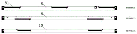
Fig. 6 shows three different types of PCBs.
Fig. 7 is a schematic diagram of the use of the clamping device for PCB bonding according to the present invention.
Reference numerals: the main part piece 1, cooperation piece 2, fixed block 3, L type bearing 4, nut 5, slide channel 6, big L type bearing 7, cuboid 41, cylinder 42, PCB 8, PCB 9, PCB 10, PCB pressfitting region 81.
Detailed Description
The following describes an implementation structure of the present invention with reference to the drawings.
As shown in fig. 1 to 5, the fixture device for pressing PCBs according to the present invention includes a main body block 1, a fitting block 2, a fixing block 3, an L-shaped support 4, and a nut 5; the main body block 1 is T-shaped, and the matching blocks 2 are arranged at two sides of the main body block 1 symmetrically; the main body block 1 and the matching block 2 are fixedly connected through the fixing block 3, and an L-shaped sliding channel 6 is formed between the main body block 1 and the matching block 2; the sliding channel 6 can accommodate a plurality of L-shaped bearings 4, and the vertical length and the horizontal length of each L-shaped bearing 4 are respectively greater than the vertical length and the horizontal length of the sliding channel 6; the L-shaped bearing 4 is formed by integrally molding a cylinder 41 with a cuboid 41 at one end and a thread at the other end, and the L-shaped bearing 4 is matched with the nut 5 in a threaded connection mode to be aligned with a pressing area 81 of the PCB 8.
Further, fixed block 3 is the U type, main part piece 1, cooperation piece 2 and fixed block 3 are connected fixedly for the integration.
Further, the height of the fixing block 3 is greater than that of the cuboid 41 in the L-shaped support 4.
Furthermore, the PCB fixing device also comprises a large L-shaped support 7 which is higher than the L-shaped support 4 and is respectively arranged at two ends of the PCB 8 and used for fixing the PCB 8.
Furthermore, the vertical length of the L-shaped bearing 4 is 1-2 cm longer than that of the sliding channel 6, and the horizontal length of the L-shaped bearing 4 is 1-3 cm longer than that of the sliding channel 6.
Furthermore, the main body block 1, the matching block 2, the fixing block 3 and the L-shaped bearing 4 are all made of stainless steel materials.
As shown in fig. 6, three different types of PCBs are shown, the PCB denoted by reference numeral 8 is used as an embodiment, and the PCB stitching and fixing operation method for the other two or more types of PCBs is the same as that of the embodiment.
As shown in fig. 7, the operation process and principle of the clamping apparatus for PCB bonding of the present invention are as follows: the L-shaped bearings 4 can freely move in the L-shaped sliding channel to match the position of the PCB laminating area 81, the number of the L-shaped bearings 4 can be matched to the length which just meets the requirement of the PCB laminating area 81, two large L-shaped bearings 7 are added at the left end and the right end of the PCB after the position relation is matched to fix the position of the PCB, and the height of the cuboid of each large L-shaped bearing 7 is slightly higher than that of the other bearings 4; finally, the L-shaped support 4 and the large L-shaped support 7 are fixed through the threaded connection of the nut 5 and the cylinder 41 with the threads in the L-shaped support 4, and therefore the PCB is fixed in a pressing mode.
The fixture device for pressing the PCB can match and press PCBs with different lengths and widths, different component positions and different pressing areas by adjusting the positions and the number of the L-shaped supports 4, and has the advantages of good clamping effect, simple structure, flexible design, material saving and convenient operation.
The above description is only an embodiment of the present invention, but the scope of the present invention is not limited thereto, and any changes or simple substitutions which are not thought of through the inventive work should be included in the scope of the present invention.
Claims (5)
1. The utility model provides a fixture device of pressfitting PCB which characterized in that: comprises a main body block (1), a matching block (2), a fixed block (3), an L-shaped support (4) and a nut (5); the main body block (1) is T-shaped, and the matching block (2) is provided with two blocks which are symmetrically arranged at two sides of the main body block (1); the main body block (1) and the matching block (2) are fixedly connected through the fixing block (3), and an L-shaped sliding channel (6) is formed between the main body block (1) and the matching block (2); the sliding channel (6) can accommodate a plurality of L-shaped bearings (4), and the vertical length and the horizontal length of each L-shaped bearing (4) are respectively greater than the vertical length and the horizontal length of the sliding channel (6); the L-shaped support (4) is formed by integrally molding a cylinder (42) with a cuboid (41) at one end and a thread at the other end, and the L-shaped support (4) is in threaded connection with the nut (5) and matched with a pressing area (81) of the PCB (8); and two ends of the PCB (8) are respectively added with a large L-shaped bearing (7) higher than the L-shaped bearing (4) for fixing the PCB (8).
2. The fixture apparatus for pressing PCBs as recited in claim 1, further comprising: the fixed block (3) is U-shaped, and the main body block (1), the matching block (2) and the fixed block (3) are connected and fixed in an integrated manner.
3. The jig device for caulking a PCB according to claim 1 or 2, wherein: the height of the fixing block (3) is greater than that of a cuboid (41) in the L-shaped support (4).
4. The fixture apparatus for pressing PCBs as recited in claim 1, further comprising: the vertical length of the L-shaped bearing (4) is 1-2 cm longer than that of the sliding channel (6), and the horizontal length of the L-shaped bearing (4) is 1-3 cm longer than that of the sliding channel (6).
5. The fixture apparatus for pressing PCBs as recited in claim 1, further comprising: the main body block (1), the matching block (2), the fixing block (3) and the L-shaped bearing (4) are all made of stainless steel materials.
Priority Applications (1)
| Application Number | Priority Date | Filing Date | Title |
|---|---|---|---|
| CN201711228158.4A CN108200720B (en) | 2017-11-29 | 2017-11-29 | Clamp device for pressing PCB |
Applications Claiming Priority (1)
| Application Number | Priority Date | Filing Date | Title |
|---|---|---|---|
| CN201711228158.4A CN108200720B (en) | 2017-11-29 | 2017-11-29 | Clamp device for pressing PCB |
Publications (2)
| Publication Number | Publication Date |
|---|---|
| CN108200720A CN108200720A (en) | 2018-06-22 |
| CN108200720B true CN108200720B (en) | 2020-01-14 |
Family
ID=62573355
Family Applications (1)
| Application Number | Title | Priority Date | Filing Date |
|---|---|---|---|
| CN201711228158.4A Active CN108200720B (en) | 2017-11-29 | 2017-11-29 | Clamp device for pressing PCB |
Country Status (1)
| Country | Link |
|---|---|
| CN (1) | CN108200720B (en) |
Families Citing this family (1)
| Publication number | Priority date | Publication date | Assignee | Title |
|---|---|---|---|---|
| CN113172405A (en) * | 2021-04-19 | 2021-07-27 | 湖北宏博汽车工业智能装备有限公司 | Multi-pressure-head automatic switching type press-fitting equipment |
Citations (4)
| Publication number | Priority date | Publication date | Assignee | Title |
|---|---|---|---|---|
| EP0772381A1 (en) * | 1995-11-06 | 1997-05-07 | Framatome Connectors International S.A. | Method and device for fitting electronic components in a printed circuit board |
| CN201307971Y (en) * | 2008-11-28 | 2009-09-09 | 耀德精密组件科技发展(深圳)有限公司 | Laminating fixture |
| CN202242397U (en) * | 2011-09-15 | 2012-05-30 | 浙江华人数码印刷有限公司 | Hardbound book feeding positioning fixture |
| CN202565581U (en) * | 2012-03-13 | 2012-11-28 | 嘉联益科技股份有限公司 | Smoothing jig |
Family Cites Families (1)
| Publication number | Priority date | Publication date | Assignee | Title |
|---|---|---|---|---|
| JP2002283533A (en) * | 2001-03-27 | 2002-10-03 | Ono Sokki Co Ltd | Work pressing device of printing table |
-
2017
- 2017-11-29 CN CN201711228158.4A patent/CN108200720B/en active Active
Patent Citations (4)
| Publication number | Priority date | Publication date | Assignee | Title |
|---|---|---|---|---|
| EP0772381A1 (en) * | 1995-11-06 | 1997-05-07 | Framatome Connectors International S.A. | Method and device for fitting electronic components in a printed circuit board |
| CN201307971Y (en) * | 2008-11-28 | 2009-09-09 | 耀德精密组件科技发展(深圳)有限公司 | Laminating fixture |
| CN202242397U (en) * | 2011-09-15 | 2012-05-30 | 浙江华人数码印刷有限公司 | Hardbound book feeding positioning fixture |
| CN202565581U (en) * | 2012-03-13 | 2012-11-28 | 嘉联益科技股份有限公司 | Smoothing jig |
Also Published As
| Publication number | Publication date |
|---|---|
| CN108200720A (en) | 2018-06-22 |
Similar Documents
| Publication | Publication Date | Title |
|---|---|---|
| CN103495883A (en) | V-shaped platform fixture | |
| CN105522318A (en) | Multi-degree-of-freedom MOS transistor welding frame and application method thereof | |
| CN108200720B (en) | Clamp device for pressing PCB | |
| CN103722508A (en) | PCB (printed circuit board) fixing clamp | |
| CN103737515A (en) | PCB (Printed Circuit Board) maintenance fixture | |
| CN203788576U (en) | Wave soldering fixture | |
| CN206216163U (en) | Wiring board welding system and wiring board positioning tool | |
| CN205218896U (en) | Positioning apparatus | |
| CN203831285U (en) | Vacuum table top auxiliary clamp | |
| CN207305110U (en) | A kind of pcb board cutting fast-positioning device | |
| CN110402027A (en) | A kind of multistation locating holes mechanism and its boring method for pcb board | |
| CN212444922U (en) | Novel circuit board clamping plate | |
| CN210211700U (en) | Clamping device for screen printing | |
| CN208432641U (en) | It is a kind of for testing the fixture of PCB circuit board | |
| CN207629907U (en) | A kind of assembled fixture | |
| CN203751993U (en) | PCB (printed circuit board) maintenance clamp | |
| CN205904941U (en) | Novel pin pressure equipment anchor clamps | |
| CN206963200U (en) | Multifunctional jig | |
| CN203330740U (en) | Work-piece clamping device for PCB drilling machine | |
| CN202206733U (en) | Butting locating type buckle mechanism | |
| CN205441779U (en) | A special conveyor for moving carry machine | |
| CN209206134U (en) | One kind being used for flexible circuit board bending General purpose jig | |
| CN204322153U (en) | Pcb board puncher fast compressing device | |
| CN215786022U (en) | Positioning fixture of lead frame | |
| CN210337206U (en) | Pressing device |
Legal Events
| Date | Code | Title | Description |
|---|---|---|---|
| PB01 | Publication | ||
| PB01 | Publication | ||
| SE01 | Entry into force of request for substantive examination | ||
| SE01 | Entry into force of request for substantive examination | ||
| TA01 | Transfer of patent application right |
Effective date of registration: 20190906 Address after: 518100 2nd and 5th Floors of Building B, Xijing Industrial Zone, Gushitang West Team, Xixiang, Baoan District, Shenzhen City, Guangdong Province Applicant after: Xingyuan Electronic Technology (Shenzhen) Co.,Ltd. Address before: 536000 Industrial Park, Beihai City, Guangxi Zhuang Autonomous Region, No. 3, District 4, Gaoke Road (Sanuo Intelligent Industrial Park D02) Applicant before: Beihai Yuan Yuan Electronic Technology Co., Ltd. |
|
| TA01 | Transfer of patent application right | ||
| GR01 | Patent grant | ||
| GR01 | Patent grant |