CN108121663B - Data storage method, memory storage device and memory control circuit unit - Google Patents
Data storage method, memory storage device and memory control circuit unit Download PDFInfo
- Publication number
- CN108121663B CN108121663B CN201611069469.6A CN201611069469A CN108121663B CN 108121663 B CN108121663 B CN 108121663B CN 201611069469 A CN201611069469 A CN 201611069469A CN 108121663 B CN108121663 B CN 108121663B
- Authority
- CN
- China
- Prior art keywords
- data
- unit
- space
- physical
- memory
- Prior art date
- Legal status (The legal status is an assumption and is not a legal conclusion. Google has not performed a legal analysis and makes no representation as to the accuracy of the status listed.)
- Active
Links
Images




Classifications
-
- G—PHYSICS
- G06—COMPUTING OR CALCULATING; COUNTING
- G06F—ELECTRIC DIGITAL DATA PROCESSING
- G06F12/00—Accessing, addressing or allocating within memory systems or architectures
- G06F12/02—Addressing or allocation; Relocation
- G06F12/0223—User address space allocation, e.g. contiguous or non contiguous base addressing
- G06F12/023—Free address space management
- G06F12/0238—Memory management in non-volatile memory, e.g. resistive RAM or ferroelectric memory
- G06F12/0246—Memory management in non-volatile memory, e.g. resistive RAM or ferroelectric memory in block erasable memory, e.g. flash memory
-
- G—PHYSICS
- G06—COMPUTING OR CALCULATING; COUNTING
- G06F—ELECTRIC DIGITAL DATA PROCESSING
- G06F12/00—Accessing, addressing or allocating within memory systems or architectures
- G06F12/02—Addressing or allocation; Relocation
- G06F12/0223—User address space allocation, e.g. contiguous or non contiguous base addressing
- G06F12/023—Free address space management
- G06F12/0238—Memory management in non-volatile memory, e.g. resistive RAM or ferroelectric memory
Landscapes
- Engineering & Computer Science (AREA)
- Theoretical Computer Science (AREA)
- Physics & Mathematics (AREA)
- General Engineering & Computer Science (AREA)
- General Physics & Mathematics (AREA)
- Techniques For Improving Reliability Of Storages (AREA)
Abstract
Description
技术领域technical field
本发明涉及一种存储器管理机制,且尤其涉及一种数据存储方法、存储器存储装置及存储器控制电路单元。The present invention relates to a memory management mechanism, and more particularly, to a data storage method, a memory storage device and a memory control circuit unit.
背景技术Background technique
数码相机、移动电话与MP3播放器在这几年来的成长十分迅速,使得消费者对存储介质的需求也急速增加。由于可复写式非易失性存储器模块(例如,闪存存储器)具有数据非易失性、省电、体积小,以及无机械结构等特性,所以非常适合内建于上述所举例的各种便携式多媒体装置中。Digital cameras, mobile phones and MP3 players have grown rapidly over the past few years, resulting in a rapid increase in consumer demand for storage media. Since the rewritable non-volatile memory module (eg, flash memory) has the characteristics of data non-volatility, power saving, small size, and no mechanical structure, it is very suitable for various portable multimedia built in the above examples. in the device.
一般来说,当存储器装置出厂时,存储器装置中会配置有一预设数目的闲置实体区块。当欲存储数据时,其中的一个闲置实体区块会被使用以存储此数据。然而,随着越来越多的数据被存入存储器装置中,越来越多的闲置实体区块会被使用并且使得闲置实体区块的数目逐渐减少。当存储器装置中闲置实体区块的数目减少到一特定数目时,存储器装置会执行一数据整并操作(也称为垃圾收集操作),以尝试释放出新的闲置实体区块。Generally, when a memory device is shipped from the factory, a predetermined number of idle physical blocks are configured in the memory device. When data is to be stored, one of the free physical blocks will be used to store the data. However, as more and more data is stored in the memory device, more and more idle physical blocks are used and the number of idle physical blocks gradually decreases. When the number of free physical blocks in the memory device is reduced to a certain number, the memory device performs a data consolidation operation (also called a garbage collection operation) to try to release new free physical blocks.
在数据整并操作中,存储器装置会从一或多个来源节点(例如,一个来源节点是存储器装置的一个实体区块)中收集有效数据并将收集的数据集中存储至一个回收节点(例如,一个回收节点也为存储器装置的一个实体区块)。若某一个实体区块(即,来源节点)所存储的有效数据皆已被收集,则此实体区块会被抹除并且视为一个新的闲置实体区块。然而,在某些情况下,若未对来源节点的数量以及所收集的数据进行适当地规划,则当回收节点被写满时,可能仍没有任何实体区块可以被抹除。换言之,在此情况下,所执行的数据整并操作可能无法释放出任何新的闲置实体区块,使得存储器装置无法正常运作。In a data consolidation operation, the memory device collects valid data from one or more source nodes (eg, a source node is a physical block of the memory device) and centrally stores the collected data to a recycling node (eg, A reclaim node is also a physical block of a memory device). If all valid data stored in a physical block (ie, the source node) has been collected, the physical block will be erased and regarded as a new idle physical block. However, in some cases, if the number of source nodes and the data collected are not properly planned, when the recycling nodes are full, there may still be no physical blocks that can be erased. In other words, in this case, the performed data consolidation operation may not release any new idle physical blocks, so that the memory device cannot operate normally.
发明内容SUMMARY OF THE INVENTION
本发明提供一种数据存储方法、存储器存储装置及存储器控制电路单元,可确保存储器存储装置在多来源节点的数据整并操作中释放出至少一个闲置实体单元。The present invention provides a data storage method, a memory storage device and a memory control circuit unit, which can ensure that the memory storage device releases at least one idle physical unit in the data consolidation operation of multi-source nodes.
本发明的一范例实施例提供一种数据存储方法,其用于包括多个实体单元的可复写式非易失性存储器模块,所述数据存储方法包括:在所述多个实体单元中的第一实体单元中决定第一空间;以及将所述多个实体单元中的至少一个实体单元所存储的至少部分数据存储至该第一实体单元中不属于该第一空间的第二空间,其中该第一空间用以确保所述至少一实体单元中的至少一第二实体单元所存储的有效数据会被存入该第一实体单元中。An exemplary embodiment of the present invention provides a data storage method for a rewritable non-volatile memory module including a plurality of physical units, the data storage method comprising: a first data storage method in the plurality of physical units A first space is determined in a physical unit; and at least part of the data stored in at least one of the plurality of physical units is stored in a second space that does not belong to the first space in the first physical unit, wherein the The first space is used to ensure that valid data stored in at least one second physical unit in the at least one physical unit will be stored in the first physical unit.
在本发明的一范例实施例中,在所述多个实体单元中的所述第一实体单元中决定所述第一空间的步骤包括:根据所述至少一第二实体单元所存储的有效数据的总数据量决定所述第一空间的初始容量,其中所述至少一第二实体单元所存储的有效数据的总数据量与所述第一空间的所述初始容量一致。In an exemplary embodiment of the present invention, the step of determining the first space in the first physical unit of the plurality of physical units includes: according to valid data stored in the at least one second physical unit The total data volume of the first space determines the initial capacity of the first space, wherein the total data volume of valid data stored by the at least one second physical unit is consistent with the initial capacity of the first space.
在本发明的一范例实施例中,所述数据存储方法还包括:若所述至少部分数据包括来自于所述至少一第二实体单元的第一数据,将所述第一空间的容量从第一容量改变为第二容量,其中所述第二容量少于所述第一容量。In an exemplary embodiment of the present invention, the data storage method further includes: if the at least part of the data includes the first data from the at least one second physical unit, changing the capacity of the first space from the first A capacity is changed to a second capacity, wherein the second capacity is less than the first capacity.
在本发明的一范例实施例中,所述数据存储方法还包括:若所述至少部分数据不包括来自所述至少一第二实体单元的第一数据,不改变所述第一空间的容量。In an exemplary embodiment of the present invention, the data storage method further includes: if the at least part of the data does not include the first data from the at least one second physical unit, not changing the capacity of the first space.
在本发明的一范例实施例中,所述数据存储方法还包括:若所述第二空间被所述至少部分数据写满,将来自所述至少一第二实体单元的剩余数据存储至所述第一空间,且不将来自所述至少一实体单元中的第三实体单元的数据存入所述第一空间。In an exemplary embodiment of the present invention, the data storage method further includes: if the second space is filled with the at least part of the data, storing the remaining data from the at least one second physical unit to the at least one second physical unit. a first space, and data from a third physical unit of the at least one physical unit is not stored in the first space.
在本发明的一范例实施例中,所述数据存储方法还包括:若所述至少部分数据包括来自所述至少一第二实体单元的第一数据,不改变所述第一空间的容量。In an exemplary embodiment of the present invention, the data storage method further includes: if the at least part of the data includes the first data from the at least one second physical unit, not changing the capacity of the first space.
本发明的另一范例实施例提供一种存储器存储装置,其包括连接接口单元、可复写式非易失性存储器模块及存储器控制电路单元。所述连接接口单元用以连接至主机系统。所述可复写式非易失性存储器模块包括多个实体单元。所述存储器控制电路单元连接至所述连接接口单元与所述可复写式非易失性存储器模块。所述存储器控制电路单元用以在所述多个实体单元中的第一实体单元中决定第一空间。所述存储器控制电路单元还用以发送至少一第一写入指令序列,以指示将所述多个实体单元中的至少一个实体单元所存储的至少部分数据存储至所述第一实体单元中不属于所述第一空间的第二空间,其中所述第一空间用以确保所述至少一实体单元中的至少一第二实体单元所存储的有效数据会被存入所述第一实体单元中。Another exemplary embodiment of the present invention provides a memory storage device including a connection interface unit, a rewritable nonvolatile memory module, and a memory control circuit unit. The connection interface unit is used for connecting to the host system. The rewritable non-volatile memory module includes a plurality of physical units. The memory control circuit unit is connected to the connection interface unit and the rewritable nonvolatile memory module. The memory control circuit unit is used for determining a first space in a first physical unit of the plurality of physical units. The memory control circuit unit is further configured to send at least one first write command sequence to instruct to store at least part of the data stored in at least one of the plurality of physical units into the first physical unit not to. a second space belonging to the first space, wherein the first space is used to ensure that valid data stored in at least one second physical unit of the at least one physical unit will be stored in the first physical unit .
在本发明的一范例实施例中,所述存储器控制电路单元在所述多个实体单元中的所述第一实体单元中决定所述第一空间的操作包括:根据所述至少一第二实体单元所存储的有效数据的总数据量决定所述第一空间的初始容量,其中所述至少一第二实体单元所存储的有效数据的总数据量与所述第一空间的所述初始容量一致。In an exemplary embodiment of the present invention, the operation of the memory control circuit unit determining the first space in the first physical unit of the plurality of physical units includes: according to the at least one second physical unit The total data volume of valid data stored in the unit determines the initial capacity of the first space, wherein the total data volume of valid data stored by the at least one second physical unit is consistent with the initial volume of the first space .
在本发明的一范例实施例中,若所述至少部分数据包括来自于所述至少一第二实体单元的第一数据,所述存储器控制电路单元还用以将所述第一空间的容量从第一容量改变为第二容量,其中所述第二容量少于所述第一容量。In an exemplary embodiment of the present invention, if the at least part of the data includes the first data from the at least one second physical unit, the memory control circuit unit is further configured to change the capacity of the first space from The first capacity is changed to a second capacity, wherein the second capacity is less than the first capacity.
在本发明的一范例实施例中,若所述至少部分数据不包括来自所述至少一第二实体单元的第一数据,所述存储器控制电路单元不改变所述第一空间的容量。In an exemplary embodiment of the present invention, if the at least part of the data does not include the first data from the at least one second physical unit, the memory control circuit unit does not change the capacity of the first space.
在本发明的一范例实施例中,若所述第二空间被所述至少部分数据写满,所述存储器控制电路单元还用以发送至少一第二写入指令序列,以指示将来自所述至少一第二实体单元的剩余数据存储至所述第一空间,且所述存储器控制电路单元不将来自所述至少一实体单元中的第三实体单元的数据存入所述第一空间。In an exemplary embodiment of the present invention, if the second space is filled with the at least part of the data, the memory control circuit unit is further configured to send at least one second write command sequence to instruct The remaining data of at least one second physical unit is stored in the first space, and the memory control circuit unit does not store data from a third physical unit of the at least one physical unit in the first space.
在本发明的一范例实施例中,若所述至少部分数据包括来自所述至少一第二实体单元的第一数据,所述存储器控制电路单元不改变所述第一空间的容量。In an exemplary embodiment of the present invention, if the at least part of the data includes the first data from the at least one second physical unit, the memory control circuit unit does not change the capacity of the first space.
本发明的另一范例实施例提供一种存储器控制电路单元,其用于控制包括多个实体单元的可复写式非易失性存储器模块,所述存储器控制电路单元包括主机接口、存储器接口及存储器管理电路。所述主机接口用以连接至主机系统。所述存储器接口用以连接至所述可复写式非易失性存储器模块。所述存储器管理电路连接至所述主机接口与所述存储器接口。所述存储器管理电路用以在所述多个实体单元中的第一实体单元中决定第一空间。所述存储器管理电路还用以发送至少一第一写入指令序列,以指示将所述多个实体单元中的至少一个实体单元所存储的至少部分数据存储至所述第一实体单元中不属于所述第一空间的第二空间,其中所述第一空间用以确保所述至少一实体单元中的至少一第二实体单元所存储的有效数据会被存入所述第一实体单元中。Another exemplary embodiment of the present invention provides a memory control circuit unit for controlling a rewritable non-volatile memory module including a plurality of physical units, the memory control circuit unit including a host interface, a memory interface and a memory management circuit. The host interface is used to connect to a host system. The memory interface is used to connect to the rewritable non-volatile memory module. The memory management circuit is connected to the host interface and the memory interface. The memory management circuit is used for determining a first space in a first physical unit of the plurality of physical units. The memory management circuit is further configured to send at least one first write command sequence to instruct to store at least part of the data stored in at least one of the plurality of physical units into the first physical unit that does not belong to the The second space of the first space, wherein the first space is used to ensure that valid data stored in at least one second physical unit of the at least one physical unit will be stored in the first physical unit.
在本发明的一范例实施例中,所述存储器管理电路在所述多个实体单元中的所述第一实体单元中决定所述第一空间的操作包括:根据所述至少一第二实体单元所存储的有效数据的总数据量决定所述第一空间的初始容量,其中所述至少一第二实体单元所存储的有效数据的总数据量与所述第一空间的所述初始容量一致。In an exemplary embodiment of the present invention, the operation of the memory management circuit determining the first space in the first physical unit of the plurality of physical units includes: according to the at least one second physical unit The total data volume of the stored valid data determines the initial capacity of the first space, wherein the total data volume of valid data stored by the at least one second physical unit is consistent with the initial volume of the first space.
在本发明的一范例实施例中,若所述至少部分数据包括来自于所述至少一第二实体单元的第一数据,所述存储器管理电路还用以将所述第一空间的容量从第一容量改变为第二容量,其中所述第二容量少于所述第一容量。In an exemplary embodiment of the present invention, if the at least part of the data includes the first data from the at least one second physical unit, the memory management circuit is further configured to change the capacity of the first space from the first A capacity is changed to a second capacity, wherein the second capacity is less than the first capacity.
在本发明的一范例实施例中,所述第一容量与所述第二容量之间的差值与所述第一数据的数据量一致。In an exemplary embodiment of the present invention, the difference between the first capacity and the second capacity is consistent with the data amount of the first data.
在本发明的一范例实施例中,所述第一空间的容量正相关于所述至少一第二实体单元中未被存储至所述第一实体单元的有效数据的总数据量。In an exemplary embodiment of the present invention, the capacity of the first space is positively related to the total data amount of valid data in the at least one second physical unit that is not stored in the first physical unit.
在本发明的一范例实施例中,若所述至少一第二实体单元所存储的所有有效数据皆被存入所述第二空间中,则所述第二空间的容量等于所述第一实体单元的总容量。In an exemplary embodiment of the present invention, if all valid data stored in the at least one second entity unit is stored in the second space, the capacity of the second space is equal to that of the first entity The total capacity of the unit.
在本发明的一范例实施例中,若所述至少部分数据不包括来自所述至少一第二实体单元的第一数据,所述存储器管理电路不改变所述第一空间的容量。In an exemplary embodiment of the present invention, if the at least part of the data does not include the first data from the at least one second physical unit, the memory management circuit does not change the capacity of the first space.
在本发明的一范例实施例中,若所述第二空间被所述至少部分数据写满,所述存储器管理电路还用以发送至少一第二写入指令序列,以指示将来自所述至少一第二实体单元的剩余数据存储至所述第一空间,且所述存储器管理电路不将来自所述至少一实体单元中的第三实体单元的数据存入所述第一空间。In an exemplary embodiment of the present invention, if the second space is filled with the at least part of the data, the memory management circuit is further configured to send at least one second write command sequence to indicate that the at least one Remaining data of a second physical unit is stored in the first space, and the memory management circuit does not store data from a third physical unit of the at least one physical unit in the first space.
在本发明的一范例实施例中,若所述至少部分数据包括来自所述至少一第二实体单元的第一数据,所述存储器管理电路不改变所述第一空间的容量。In an exemplary embodiment of the present invention, if the at least part of the data includes the first data from the at least one second physical unit, the memory management circuit does not change the capacity of the first space.
基于上述,通过预先在第一实体单元中决定保留给来自于第二实体单元的数据使用的第一空间,本发明可确保存储器存储装置在多来源节点的数据整并操作中释放出至少一个闲置实体单元。Based on the above, by predetermining the first space reserved for the data from the second physical unit in the first physical unit, the present invention can ensure that the memory storage device releases at least one idle space during the data consolidation operation of the multi-source nodes. entity unit.
为让本发明的上述特征和优点能更明显易懂,下文特举实施例,并配合附图作详细说明如下。In order to make the above-mentioned features and advantages of the present invention more obvious and easy to understand, the following embodiments are given and described in detail with the accompanying drawings as follows.
附图说明Description of drawings
图1是根据本发明的一范例实施例所示出的主机系统、存储器存储装置及输入/输出(I/O)装置的示意图。FIG. 1 is a schematic diagram of a host system, a memory storage device, and an input/output (I/O) device according to an exemplary embodiment of the present invention.
图2是根据本发明的另一范例实施例所示出的主机系统、存储器存储装置及I/O装置的示意图。FIG. 2 is a schematic diagram of a host system, a memory storage device, and an I/O device according to another exemplary embodiment of the present invention.
图3是根据本发明的另一范例实施例所示出的主机系统与存储器存储装置的示意图。FIG. 3 is a schematic diagram of a host system and a memory storage device according to another exemplary embodiment of the present invention.
图4是根据本发明的一范例实施例所示出的存储器存储装置的概要框图。FIG. 4 is a schematic block diagram of a memory storage device according to an exemplary embodiment of the present invention.
图5是根据本发明的一范例实施例所示出的存储器控制电路单元的概要框图。FIG. 5 is a schematic block diagram of a memory control circuit unit according to an exemplary embodiment of the present invention.
图6是根据本发明的一范例实施例所示出的管理可复写式非易失性存储器模块的示意图。FIG. 6 is a schematic diagram of managing a rewritable non-volatile memory module according to an exemplary embodiment of the present invention.
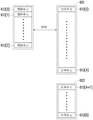
图7是根据本发明的一范例实施例所示出的数据整并操作的前置处理的示意图。FIG. 7 is a schematic diagram of preprocessing of a data consolidation operation according to an exemplary embodiment of the present invention.
图8A至8E是根据本发明的一范例实施例所示出的数据整并操作的示意图。8A to 8E are schematic diagrams illustrating a data consolidation operation according to an exemplary embodiment of the present invention.
图8F是根据本发明的另一范例实施例所示出的数据整并操作的示意图。FIG. 8F is a schematic diagram of a data consolidation operation according to another exemplary embodiment of the present invention.
图8G是根据本发明的另一范例实施例所示出的数据整并操作的示意图。FIG. 8G is a schematic diagram of a data consolidation operation according to another exemplary embodiment of the present invention.
图8H是根据本发明的另一范例实施例所示出的数据整并操作的示意图。FIG. 8H is a schematic diagram illustrating a data consolidation operation according to another exemplary embodiment of the present invention.
图9是根据本发明的一范例实施例所示出的数据存储方法的流程图。FIG. 9 is a flowchart of a data storage method according to an exemplary embodiment of the present invention.
图10是根据本发明的另一范例实施例所示出的数据存储方法的流程图。FIG. 10 is a flowchart of a data storage method according to another exemplary embodiment of the present invention.
附图标号说明:Description of reference numbers:
10、30:存储器存储装置;10, 30: memory storage device;
11:主机系统;11: host system;
110:系统总线;110: system bus;
111:处理器;111: processor;
112:随机存取存储器;112: random access memory;
113:只读存储器;113: read-only memory;
114:数据传输接口;114: data transmission interface;
12:输入/输出(I/O)装置;12: Input/output (I/O) device;
20:主机板;20: motherboard;
201:U盘;201: U disk;
202:内存卡;202: memory card;
203:固态硬盘;203: SSD;
204:无线存储器存储装置;204: wireless memory storage device;
205:全球定位系统模块;205: GPS module;
206:网络接口卡;206: network interface card;
207:无线传输装置;207: wireless transmission device;
208:键盘;208: keyboard;
209:屏幕;209: screen;
210:喇叭;210: horn;
32:SD卡;32: SD card;
33:CF卡;33: CF card;
34:嵌入式存储装置;34: embedded storage device;
341:嵌入式多媒体卡;341: embedded multimedia card;
342:嵌入式多芯片封装存储装置;342: an embedded multi-chip package storage device;
402:连接接口单元;402: connect the interface unit;
404:存储器控制电路单元;404: memory control circuit unit;
406:可复写式非易失性存储器模块;406: rewritable non-volatile memory module;
502:存储器管理电路;502: memory management circuit;
504:主机接口;504: host interface;
506:存储器接口;506: memory interface;
508:错误检查与校正电路;508: Error checking and correction circuit;
510:缓冲存储器;510: buffer memory;
512:电源管理电路;512: power management circuit;
601:缓冲区;601: buffer;
602:存储区;602: storage area;
610(0)~610(B)、710(1)~710(3):实体单元;610(0)~610(B), 710(1)~710(3): entity unit;
612(0)~612(C):逻辑单元;612(0)~612(C): logic unit;
701、703:有效数据;701, 703: valid data;
702、704:无效数据;702, 704: invalid data;
721、722:空间;721, 722: space;
730:指标;730: indicator;
801~804:数据;801~804: data;
811(0)~811(M):实体编程单元;811(0)~811(M): entity programming unit;
S901:步骤(在可复写式非易失性存储器模块的第一实体单元中决定第一空间);S901: step (determining the first space in the first physical unit of the rewritable non-volatile memory module);
S902:步骤(将可复写式非易失性存储器模块的至少一实体单元所存储的至少部分数据存储至第一实体单元中不属于第一空间的第二空间);S902: step (storing at least part of the data stored in at least one physical unit of the rewritable non-volatile memory module into a second space that does not belong to the first space in the first physical unit);
S1001:步骤(在可复写式非易失性存储器模块中选择第一实体单元、第二实体单元及第三实体单元);S1001: step (selecting the first physical unit, the second physical unit and the third physical unit in the rewritable non-volatile memory module);
S1002:步骤(在第一实体单元中决定第一空间);S1002: step (determining the first space in the first entity unit);
S1003:步骤(从第二实体单元和/或第三实体单元中收集有效数据);S1003: step (collect valid data from the second entity unit and/or the third entity unit);
S1004:步骤(第一实体单元中不属于第一空间的第二空间是否被写满);S1004: step (whether the second space in the first entity unit that does not belong to the first space is full);
S1005:步骤(将所收集的数据存储至第二空间);S1005: step (store the collected data in the second space);
S1006:步骤(所存储的数据是否包含来自第二实体单元的数据);S1006: step (whether the stored data includes data from the second entity unit);
S1007:步骤(减少第一空间的容量);S1007: step (reduce the capacity of the first space);
S1008:步骤(将来自第二实体单元的数据存储至第一空间并且停止存储来自第三实体单元的数据)。S1008: Step (store the data from the second physical unit to the first space and stop storing the data from the third physical unit).
具体实施方式Detailed ways
一般而言,存储器存储装置(也称,存储器存储系统)包括可复写式非易失性存储器模块(rewritable non-volatile memory module)与控制器(也称,控制电路)。通常存储器存储装置是与主机系统一起使用,以使主机系统可将数据写入至存储器存储装置或从存储器存储装置中读取数据。In general, a memory storage device (also referred to as a memory storage system) includes a rewritable non-volatile memory module and a controller (also referred to as a control circuit). Typically a memory storage device is used with a host system so that the host system can write data to or read data from the memory storage device.
图1是根据本发明的一范例实施例所示出的主机系统、存储器存储装置及输入/输出(I/O)装置的示意图。图2是根据本发明的另一范例实施例所示出的主机系统、存储器存储装置及I/O装置的示意图。FIG. 1 is a schematic diagram of a host system, a memory storage device, and an input/output (I/O) device according to an exemplary embodiment of the present invention. FIG. 2 is a schematic diagram of a host system, a memory storage device, and an I/O device according to another exemplary embodiment of the present invention.
请参照图1与图2,主机系统11一般包括处理器111、随机存取存储器(randomaccess memory,RAM)112、只读存储器(read only memory,ROM)113及数据传输接口114。处理器111、随机存取存储器112、只读存储器113及数据传输接口114皆连接至系统总线(system bus)110。Referring to FIGS. 1 and 2 , the
在本范例实施例中,主机系统11是通过数据传输接口114与存储器存储装置10连接。例如,主机系统11可经由数据传输接口114将数据存储至存储器存储装置10或从存储器存储装置10中读取数据。此外,主机系统11是通过系统总线110与I/O装置12连接。例如,主机系统11可经由系统总线110将输出信号传送至I/O装置12或从I/O装置12接收输入信号。In this exemplary embodiment, the
在本范例实施例中,处理器111、随机存取存储器112、只读存储器113及数据传输接口114可设置在主机系统11的主机板20上。数据传输接口114的数目可以是一或多个。通过数据传输接口114,主机板20可以经由有线或无线方式连接至存储器存储装置10。存储器存储装置10可例如是U盘201、内存卡202、固态硬盘(Solid State Drive,SSD)203或无线存储器存储装置204。无线存储器存储装置204可例如是近距离无线通信(Near FieldCommunication,NFC)存储器存储装置、无线保真(WiFi)存储器存储装置、蓝牙(Bluetooth)存储器存储装置或低功耗蓝牙存储器存储装置(例如,iBeacon)等以各式无线通信技术为基础的存储器存储装置。此外,主机板20也可以通过系统总线110连接至全球定位系统(Global Positioning System,GPS)模块205、网络接口卡206、无线传输装置207、键盘208、屏幕209、喇叭210等各式I/O装置。例如,在一范例实施例中,主机板20可通过无线传输装置207存取无线存储器存储装置204。In this exemplary embodiment, the
在一范例实施例中,所提及的主机系统为可实质地与存储器存储装置配合以存储数据的任意系统。虽然在上述范例实施例中,主机系统是以电脑系统来作说明,然而,图3是根据本发明的另一范例实施例所示出的主机系统与存储器存储装置的示意图。请参照图3,在另一范例实施例中,主机系统31也可以是数码相机、摄像机、通信装置、音频播放器、视频播放器或平板电脑等系统,而存储器存储装置30可为其所使用的安全数字(SecureDigital,SD)卡32、小型闪存(Compact Flash,CF)卡33或嵌入式存储装置34等各式非易失性存储器存储装置。嵌入式存储装置34包括嵌入式多媒体卡(embedded Multi MediaCard,eMMC)341和/或嵌入式多芯片封装(embedded Multi Chip Package,eMCP)存储装置342等各类型将存储器模块直接连接于主机系统的基板上的嵌入式存储装置。In an example embodiment, reference to a host system is substantially any system that can cooperate with a memory storage device to store data. Although in the above exemplary embodiment, the host system is described as a computer system, FIG. 3 is a schematic diagram of a host system and a memory storage device according to another exemplary embodiment of the present invention. Referring to FIG. 3 , in another exemplary embodiment, the
图4是根据本发明的一范例实施例所示出的存储器存储装置的概要框图。FIG. 4 is a schematic block diagram of a memory storage device according to an exemplary embodiment of the present invention.
请参照图4,存储器存储装置10包括连接接口单元402、存储器控制电路单元404与可复写式非易失性存储器模块406。Referring to FIG. 4 , the
连接接口单元402用以将存储器存储装置10连接至主机系统11。在本范例实施例中,连接接口单元402是相容于序列先进附件(Serial Advanced Technology Attachment,SATA)标准。然而,必须了解的是,本发明不限于此,连接接口单元402也可以是符合并列先进附件(Parallel Advanced Technology Attachment,PATA)标准、电气和电子工程师协会(Institute of Electrical and Electronic Engineers,IEEE)1394标准、高速周边零件连接接口(Peripheral Component Interconnect Express,PCI Express)标准、通用串行总线(Universal Serial Bus,USB)标准、SD接口标准、超高速一代(Ultra High Speed-I,UHS-I)接口标准、超高速二代(Ultra High Speed-II,UHS-II)接口标准、记忆棒(MemoryStick,MS)接口标准、MCP接口标准、MMC接口标准、eMMC接口标准、通用闪存存储器(Universal Flash Storage,UFS)接口标准、eMCP接口标准、CF接口标准、整合式驱动电子接口(Integrated Device Electronics,IDE)标准或其他适合的标准。连接接口单元402可与存储器控制电路单元404封装在一个芯片中,或者连接接口单元402是布设于一包含存储器控制电路单元404的芯片外。The
存储器控制电路单元404用以执行以硬件或软件实作的多个逻辑门或控制指令并且根据主机系统11的指令在可复写式非易失性存储器模块406中进行数据的写入、读取与抹除等运作。The memory
可复写式非易失性存储器模块406是连接至存储器控制电路单元404并且用以存储主机系统11所写入的数据。可复写式非易失性存储器模块406可以是单阶存储单元(Single Level Cell,SLC)NAND型闪存存储器模块(即,一个存储单元中可存储1个比特的闪存存储器模块)、多阶存储单元(Multi Level Cell,MLC)NAND型闪存存储器模块(即,一个存储单元中可存储2个比特的闪存存储器模块)、复数阶存储单元(Triple Level Cell,TLC)NAND型闪存存储器模块(即,一个存储单元中可存储3个比特的闪存存储器模块)、其他闪存存储器模块或其他具有相同特性的存储器模块。The rewritable
可复写式非易失性存储器模块406中的每一个存储单元是以电压(以下也称为临界电压)的改变来存储一或多个比特。具体来说,每一个存储单元的控制栅极(controlgate)与通道之间有一个电荷捕捉层。通过施予一写入电压至控制栅极,可以改变电荷补捉层的电子量,进而改变存储单元的临界电压。此改变存储单元的临界电压的操作也称为“把数据写入至存储单元”或“编程(programming)存储单元”。随着临界电压的改变,可复写式非易失性存储器模块406中的每一个存储单元具有多个存储状态。通过施予读取电压可以判断一个存储单元是属于哪一个存储状态,借此取得此存储单元所存储的一或多个比特。Each memory cell in the rewritable
在本范例实施例中,可复写式非易失性存储器模块406的存储单元会构成多个实体编程单元,并且此些实体编程单元会构成多个实体抹除单元。具体来说,同一条字线上的存储单元会组成一或多个实体编程单元。若每一个存储单元可存储2个以上的比特,则同一条字线上的实体编程单元至少可被分类为下实体编程单元与上实体编程单元。例如,一存储单元的最低有效比特(Least Significant Bit,LSB)是属于下实体编程单元,并且一存储单元的最高有效比特(Most Significant Bit,MSB)是属于上实体编程单元。一般来说,在MLC NAND型闪存存储器中,下实体编程单元的写入速度会大于上实体编程单元的写入速度,和/或下实体编程单元的可靠度是高于上实体编程单元的可靠度。In this exemplary embodiment, the memory cells of the rewritable
在本范例实施例中,实体编程单元为编程的最小单元。即,实体编程单元为写入数据的最小单元。例如,实体编程单元为实体页面(page)或是实体扇(sector)。若实体编程单元为实体页面,则此些实体编程单元通常包括数据比特区与冗余(redundancy)比特区。数据比特区包含多个实体扇,用以存储使用者数据,而冗余比特区用以存储系统数据(例如,错误更正码等管理数据)。在本范例实施例中,数据比特区包含32个实体扇,且一个实体扇的大小为512比特组(byte,B)。然而,在其他范例实施例中,数据比特区中也可包含8个、16个或数目更多或更少的实体扇,并且每一个实体扇的大小也可以是更大或更小。另一方面,实体抹除单元为抹除的最小单位。也即,每一实体抹除单元含有最小数目之一并被抹除的存储单元。例如,实体抹除单元为实体区块(block)。In this exemplary embodiment, the physical programming unit is the smallest unit of programming. That is, the physical programming unit is the smallest unit in which data is written. For example, an entity programming unit is an entity page or an entity sector. If the physical programming unit is a physical page, the physical programming unit usually includes a data bit region and a redundancy bit region. The data bit area includes a plurality of physical sectors for storing user data, and the redundant bit area is used for storing system data (eg, management data such as error correction codes). In this exemplary embodiment, the data bit area includes 32 physical sectors, and the size of one physical sector is 512 bits (byte, B). However, in other exemplary embodiments, the data bit region may also include 8, 16, or more or less physical sectors, and the size of each physical sector may also be larger or smaller. On the other hand, the physical erasing unit is the smallest unit of erasing. That is, each physical erase unit contains a minimum number of memory units that are erased. For example, the physical erasing unit is a physical block.
图5是根据本发明的一范例实施例所示出的存储器控制电路单元的概要框图。FIG. 5 is a schematic block diagram of a memory control circuit unit according to an exemplary embodiment of the present invention.
请参照图5,存储器控制电路单元404包括存储器管理电路502、主机接口504及存储器接口506。Referring to FIG. 5 , the memory
存储器管理电路502用以控制存储器控制电路单元404的整体运作。具体来说,存储器管理电路502具有多个控制指令,并且在存储器存储装置10运作时,此些控制指令会被执行以进行数据的写入、读取与抹除等运作。以下说明存储器管理电路502的操作时,等同于说明存储器控制电路单元404的操作。The
在本范例实施例中,存储器管理电路502的控制指令是以软件来实作。例如,存储器管理电路502具有微处理器单元(未示出)与只读存储器(未示出),并且此些控制指令是被烧录至此只读存储器中。当存储器存储装置10运作时,此些控制指令会由微处理器单元来执行以进行数据的写入、读取与抹除等运作。In this exemplary embodiment, the control instructions of the
在另一范例实施例中,存储器管理电路502的控制指令也可以程序码型式存储于可复写式非易失性存储器模块406的特定区域(例如,存储器模块中专用于存放系统数据的系统区)中。此外,存储器管理电路502具有微处理器单元(未示出)、只读存储器(未示出)及随机存取存储器(未示出)。特别是,此只读存储器具有开机码(boot code),并且当存储器控制电路单元404被致能时,微处理器单元会先执行此开机码来将存储于可复写式非易失性存储器模块406中的控制指令载入至存储器管理电路502的随机存取存储器中。之后,微处理器单元会运转此些控制指令以进行数据的写入、读取与抹除等运作。In another exemplary embodiment, the control instructions of the
此外,在另一范例实施例中,存储器管理电路502的控制指令也可以一硬件来实作。例如,存储器管理电路502包括微控制器、存储单元管理电路、存储器写入电路、存储器读取电路、存储器抹除电路与数据处理电路。存储单元管理电路、存储器写入电路、存储器读取电路、存储器抹除电路与数据处理电路是连接至微控制器。存储单元管理电路用以管理可复写式非易失性存储器模块406的存储单元或其群组。存储器写入电路用以对可复写式非易失性存储器模块406下达写入指令序列以将数据写入至可复写式非易失性存储器模块406中。存储器读取电路用以对可复写式非易失性存储器模块406下达读取指令序列以从可复写式非易失性存储器模块406中读取数据。存储器抹除电路用以对可复写式非易失性存储器模块406下达抹除指令序列以将数据从可复写式非易失性存储器模块406中抹除。数据处理电路用以处理欲写入至可复写式非易失性存储器模块406的数据以及从可复写式非易失性存储器模块406中读取的数据。写入指令序列、读取指令序列及抹除指令序列可各别包括一或多个程序码或指令码并且用以指示可复写式非易失性存储器模块406执行相对应的写入、读取及抹除等操作。在一范例实施例中,存储器管理电路502还可以下达其他类型的指令序列给可复写式非易失性存储器模块406以指示执行相对应的操作。In addition, in another exemplary embodiment, the control instructions of the
主机接口504是连接至存储器管理电路502并且用以接收与识别主机系统11所传送的指令与数据。也就是说,主机系统11所传送的指令与数据会通过主机接口504来传送至存储器管理电路502。在本范例实施例中,主机接口504是相容于SATA标准。然而,必须了解的是本发明不限于此,主机接口504也可以是相容于PATA标准、IEEE 1394标准、PCIExpress标准、USB标准、SD标准、UHS-I标准、UHS-II标准、MS标准、MMC标准、eMMC标准、UFS标准、CF标准、IDE标准或其他适合的数据传输标准。The
存储器接口506是连接至存储器管理电路502并且用以存取可复写式非易失性存储器模块406。也就是说,欲写入至可复写式非易失性存储器模块406的数据会经由存储器接口506转换为可复写式非易失性存储器模块406所能接受的格式。具体来说,若存储器管理电路502要存取可复写式非易失性存储器模块406,存储器接口506会传送对应的指令序列。例如,这些指令序列可包括指示写入数据的写入指令序列、指示读取数据的读取指令序列、指示抹除数据的抹除指令序列、以及用以指示各种存储器操作(例如,改变读取电压准位或执行垃圾收集操作等等)的相对应的指令序列。这些指令序列例如是由存储器管理电路502产生并且通过存储器接口506传送至可复写式非易失性存储器模块406。这些指令序列可包括一或多个信号,或是在总线上的数据。这些信号或数据可包括指令码或程序码。例如,在读取指令序列中,会包括读取的辨识码、存储器地址等信息。The
在一范例实施例中,存储器控制电路单元404还包括错误检查与校正电路508、缓冲存储器510与电源管理电路512。In an exemplary embodiment, the memory
错误检查与校正电路508是连接至存储器管理电路502并且用以执行错误检查与校正操作以确保数据的正确性。具体来说,当存储器管理电路502从主机系统11中接收到写入指令时,错误检查与校正电路508会为对应此写入指令的数据产生对应的错误更正码(error correcting code,ECC)和/或错误检查码(error detecting code,EDC),并且存储器管理电路502会将对应此写入指令的数据与对应的错误更正码和/或错误检查码写入至可复写式非易失性存储器模块406中。之后,当存储器管理电路502从可复写式非易失性存储器模块406中读取数据时会同时读取此数据对应的错误更正码和/或错误检查码,并且错误检查与校正电路508会依据此错误更正码和/或错误检查码对所读取的数据执行错误检查与校正操作。The error checking and
缓冲存储器510是连接至存储器管理电路502并且用以暂存来自于主机系统11的数据与指令或来自于可复写式非易失性存储器模块406的数据。电源管理电路512是连接至存储器管理电路502并且用以控制存储器存储装置10的电源。The
图6是根据本发明的一范例实施例所示出的管理可复写式非易失性存储器模块的示意图。FIG. 6 is a schematic diagram of managing a rewritable non-volatile memory module according to an exemplary embodiment of the present invention.
请参照图6,存储器管理电路502会将可复写式非易失性存储器模块406的实体单元610(0)~610(B)逻辑地分组至存储区601与闲置(spare)区602。存储区601中的实体单元610(0)~610(A)存储有数据,例如,存储于存储区601的数据包括有效数据(valid data)与无效数据(invalid data),而闲置区602中的实体单元610(A+1)~610(B)尚未被用来存储数据。当欲存储数据时,存储器管理电路502会从闲置区602的实体单元610(A+1)~610(B)中选择一个实体单元并且将来自主机系统11或来自存储区601中的其他实体单元的数据存储至所选的实体单元中。同时,所选的实体单元会被关联至存储区601。此外,在抹除存储区601中的某一个实体单元后,所抹除的实体单元会被重新关联至闲置区602。Referring to FIG. 6 , the
在本范例实施例中,属于闲置区602的每一个实体单元也称为闲置实体单元,而属于存储区601的每一个实体单元也称为非闲置(non-spare)实体单元。在本范例实施例中,一个实体单元是指一个实体抹除单元。然而,在另一范例实施例中,一个实体单元也可以包含多个实体抹除单元。In this exemplary embodiment, each physical unit belonging to the
存储器管理电路502会配置逻辑单元612(0)~612(C)以映射存储区601中的实体单元610(0)~610(A)。在本范例实施例中,每一个逻辑单元是指一个逻辑地址。然而,在另一范例实施例中,一个逻辑单元也可以是指一个逻辑编程单元、一个逻辑抹除单元或者由多个连续或不连续的逻辑地址组成。此外,逻辑单元612(0)~612(C)中的每一者可被映射至一或多个实体单元。The
存储器管理电路502会将逻辑单元与实体单元之间的映射关系(也称为逻辑-实体地址映射关系)记录于至少一逻辑-实体映射表。当主机系统11欲从存储器存储装置10读取数据或写入数据至存储器存储装置10时,存储器管理电路502可根据此逻辑-实体映射表来执行对于存储器存储装置10的数据存取操作。The
在本范例实施例中,有效数据是属于某一个逻辑单元的最新数据,而无效数据则不是属于任一个逻辑单元的最新数据。例如,若主机系统11将一笔新数据存储至某一逻辑单元而覆盖掉此逻辑单元原先存储的旧数据(即,更新属于此逻辑单元的数据),则存储至存储区601中的此笔新数据即为属于此逻辑单元的最新数据并且会被标记为有效,而被覆盖掉的旧数据可能仍然存储在存储区601中但被标记为无效。In this exemplary embodiment, the valid data is the latest data belonging to a certain logic unit, and the invalid data is not the latest data belonging to any logic unit. For example, if the
在本范例实施例中,若属于某一逻辑单元的数据被更新,则此逻辑单元与存储有属于此逻辑单元的旧数据的实体单元之间的映射关系会被移除,并且此逻辑单元与存储有属于此逻辑单元的最新数据的实体单元之间的映射关系会被建立。然而,在另一范例实施例中,若属于某一逻辑单元的数据被更新,则此逻辑单元与存储有属于此逻辑单元的旧数据的实体单元之间的映射关系仍可被维持。In this exemplary embodiment, if data belonging to a logical unit is updated, the mapping relationship between the logical unit and the physical unit storing the old data belonging to the logical unit will be removed, and the logical unit and the physical unit will be removed. The mapping relationship between the entity units that store the latest data belonging to this logical unit will be established. However, in another exemplary embodiment, if the data belonging to a certain logic unit is updated, the mapping relationship between the logic unit and the physical unit storing the old data belonging to the logic unit can still be maintained.
当存储器存储装置10出厂时,属于闲置区602的实体单元的总数会是一个预设数目(例如,30)。在存储器存储装置10的运作中,越来越多的实体单元会被从闲置区602选择并且被关联至存储区601以存储数据(例如,来自主机系统11的使用者数据)。因此,属于闲置区602的实体单元的总数会随着存储器存储装置10的使用而逐渐减少。When the
在存储器存储装置10的运作中,存储器管理电路502会持续更新属于闲置区602的实体单元的总数。例如,存储器管理电路502会判断属于闲置区602的实体单元的总数是否小于或等于一个门槛值(也称为第一门槛值)。此第一门槛值例如是2或者更大的值(例如,10),本发明不加以限制。若属于闲置区602的实体单元的总数小于或等于第一门槛值,存储器管理电路502会执行一个数据整并操作。在一范例实施例中,此数据整并操作也称为垃圾收集(garbage collection)操作。During the operation of the
在数据整并操作中,存储器管理电路502会从存储区601中选择至少一个实体单元(也称为来源节点)并且尝试将有效数据从所选择的实体单元集中复制(或搬移)到另一实体单元(也称为回收节点)。用来存储所复制(或搬移)的有效数据的实体单元则是从闲置区602中选择并且会被关联至存储区601。若某一个实体单元所存储的有效数据皆已被复制(或搬移),则此实体单元会被抹除并且被关联至闲置区602。在一范例实施例中,将某一个实体单元从存储区601重新关联回闲置区602的操作也称为释放一个闲置实体单元。通过执行数据整并操作,一或多个闲置实体单元会被释放并且使得属于闲置区602的实体单元的总数逐渐增加。In a data consolidation operation, the
在开始执行数据整并操作后,若属于闲置区602的实体单元符合一特定条件,数据整并操作会停止。例如,存储器管理电路502会判断属于闲置区602的实体单元的总数是否大于或等于另一个门槛值(以下也称为第二门槛值)。例如,第二门槛值可以大于或等于第一门槛值。若属于闲置区602的实体单元的总数大于或等于第二门槛值,存储器管理电路502会停止数据整并操作。例如,停止数据整并操作是指结束当前执行中的数据整并操作。在停止一个数据整并操作之后,若属于闲置区602的实体单元的总数再次小于或等于第一门槛值,则下一个数据整并操作会再次被执行,以尝试释放新的闲置实体单元。After the data consolidation operation is started, if the physical units belonging to the
在一范例实施例中,属于闲置区602的实体单元的总数会被记载在一个管理表格中。当某一个闲置实体单元被释放时,存储器管理电路502会将此管理表格所记载的一个指示值加“1”,其中此指示值对应于属于闲置区602的实体单元的总数。当某一个实体单元被从闲置区602关联至存储区601以存储数据时,存储器管理电路502会将此指示值减“1”。在存储器存储装置10的运作中,存储器管理电路502会根据此指示值来判断是否需要执行下一个数据整并操作和/或是否要停止执行中的数据整并操作。In an exemplary embodiment, the total number of physical units belonging to the
图7是根据本发明的一范例实施例所示出的数据整并操作的前置处理的示意图。FIG. 7 is a schematic diagram of preprocessing of a data consolidation operation according to an exemplary embodiment of the present invention.
请参照图7,在实际开始搬移数据前,存储器管理电路502会选择一个实体单元(也称为第一实体单元)710(1)作为回收节点并且另外选择至少一个实体单元作为来源节点。在本范例实施力中,来源节点包括一个实体单元(也称为第二实体单元)710(2)与一个实体单元(也称为第三实体单元)710(3)。例如,实体单元710(1)是从图6的闲置区602中选择,而实体单元710(2)与710(3)则是从图6的存储区601中选择。须注意的是,虽然在本范例实施例中第二实体单元与第三实体单元的数目皆为一个,然而在另一范例实施例中,第二实体单元与第三实体单元的数目皆可为多个,本发明不加以限制。Referring to FIG. 7, before actually starting to move data, the
在决定回收节点与来源节点之后,存储器管理电路502会将实体单元710(2)与710(3)所存储的至少部分数据存储至实体单元710(1)中。例如,实体单元710(2)存储有有效数据701与无效数据702,并且实体单元710(3)存储有有效数据703与无效数据704。因此,在数据整并操作中,有效数据701与703可以被从实体单元710(2)与710(3)收集并且复制到实体单元710(1)中进行存储。此外,若实体单元710(2)与710(3)中任一者所存储的所有有效数据皆已被复制到实体单元710(1)中,则此实体单元即可被抹除。After determining the recycling node and the source node, the
另一方面,存储器管理电路502会在实体单元710(1)中决定一个空间(也称为第一空间)721。此外,空间(也称为第二空间)722是实体单元710(1)中不属于空间721的剩余空间。空间721与722分别包含连续编号的多个实体地址(或,实体编程单元)且皆可用来存放数据整并操作中收集的有效数据。On the other hand, the
在本范例实施例中,存储器管理电路502是利用指标730来在实体单元710(1)中划分空间721与722。例如,指标730可以是指到空间721中的一个起始实体地址(例如,空间721中编号最小的实体地址)或空间722中的一个结束实体地址(例如,空间722中编号最大的实体地址)。此外,在另一范例实施例中,存储器管理电路502还可以利用任何方式来在实体单元710(1)中划分空间721与722。例如,存储器管理电路502也可将空间721与722各别包含的实体地址记录于一表格中等等。In this exemplary embodiment, the
在本范例实施例中,空间721中的实体地址是排序在空间722中的实体地址之后。例如,空间721中的起始实体地址的编号是接续于空间722中的结束实体地址的编号。在将所收集的数据存入实体单元710(1)时,空间722会先被使用(即,用来存储数据)。在空间722被使用完毕(例如,被写满)之后,空间721才会接续被使用(即,用来存储数据)。In the present exemplary embodiment, the physical addresses in the
须注意的是,空间721是用来确保在最差的情况下,实体单元710(2)中的有效数据701可以被完整地存入实体单元710(1)中,使得实体单元710(2)可以被抹除。例如,最差的情况可能是有效数据701与703的总数据量超过空间721与722的总容量。换言之,若未预留空间721给有效数据701,则当实体单元710(1)被写满时,实体单元710(1)可能仅存储有效数据701中的一部分数据以及有效数据703中的一部分数据。在此情况下(即,最差的情况),实体单元710(2)与710(3)皆无法被抹除,故所执行的数据整并操作将无法释放出任何闲置实体单元。It should be noted that the
在一范例实施例中,存储器管理电路502是根据实体单元710(2)所存储的有效数据701的总数据量来决定空间721的初始容量,使得有效数据701的总数据量与空间721的初始容量一致。例如,存储器管理电路502可根据实体单元710(2)的一有效计数(validcount)来判断有效数据701的总数据量,其中此有效计数对应于实体单元710(2)中存储有有效数据701的实体编程单元的总数。根据此有效计数,存储器管理电路502可将空间721的初始容量设定为相同或相近于有效数据701的总数据量。此外,在另一范例实施例中,存储器管理电路502还可以利用一个实体-逻辑映射表来验证此有效计数,以进一步确认有效数据701的总数据量。须注意的是,所属技术领域通常知识者应当知晓如何评估某一个实体单元所存储的有效数据的数据量,故在此便不赘述。In an exemplary embodiment, the
在一范例实施例中,在选择实体单元710(2)与710(3)作为来源节点后,存储器管理电路502还会判断实体单元710(2)与710(3)中哪一者所存储的有效数据的数据量较小。例如,如图7所示,实体单元710(2)的有效数据701的数据量小于实体单元710(3)的有效数据703的数据量,故空间721的初始容量是对应于数据量较小的有效数据701设置。In an exemplary embodiment, after selecting the physical units 710(2) and 710(3) as the source node, the
须注意的是,在数据整并操作中,存储于实体单元710(2)的有效数据701与存储于实体单元710(3)的有效数据703皆可以被存储至空间722中。但是,空间721是用以确保有效数据701可以被完整地存入实体单元710(1)中。因此,在空间722被写满后,存储器管理电路502可持续将有效数据701中尚未被存储至实体单元710(1)的数据存入空间721中,而有效数据703中尚未被存储至实体单元710(1)的数据将不会被存入空间721中。借此,可确保有效数据701可被完整地存入实体单元710(1)中。It should be noted that in the data consolidation operation, both the
在一范例实施例中,空间721也可视为是用以存储来自于实体单元710(2)的数据(即,有效数据701)的保留空间,并且在数据整并操作中,空间721的容量可动态地改变。例如,在一范例实施例中,假设空间721的初始容量等于有效数据701的总数据量。在数据整并操作中,随着有效数据701中越来越多的数据被收集并存入空间722中,空间721的容量也会逐渐地被减少(因为后续可能会被存入空间721的数据的数据量越来越少)。换言之,在一范例实施例中,空间721的容量会正相关于实体单元710(2)中未被存储至实体单元710(1)的有效数据的总数据量。此外,在一范例实施例中,若存入空间722的某一数据是属于有效数据703,则存储器管理电路502并不会反应于此数据的存储而改变空间721的容量(因为后续可能会被存入空间721的数据的数据量并未减少)。更进一步,在一范例实施例中,若被存入空间722中的数据都不属于有效数据701(或者都属于有效数据703),则空间721的容量会维持在空间721的初始容量。In an exemplary embodiment,
在一范例实施例中,存储器管理电路502会判断当前存入空间722的数据是否包含来自于实体单元710(2)的数据(也称为第一数据)。例如,此第一数据是有效数据701的至少一部分。若当前存入空间722的数据包含第一数据,存储器管理电路502会减少空间721的容量。例如,存储器管理电路502会将空间721的容量从一容量(也称为第一容量)改变为另一容量(也称为第二容量),其中第二容量小于第一容量。例如,存储器管理电路502可通过调整指标730所指的实体地址来调整空间721的容量。其中,第一容量与第二容量之间的差值会与所存储的第一数据的数据量一致。例如,若第一数据的数据量等于一预设数目的实体编程单元的容量,则第一容量与第二容量之间的差值也会是此预设数目的实体编程单元的容量。此外,若当前存入空间722的数据不包含来自实体单元710(2)的数据(例如,当前存入空间722的数据仅属于有效数据703),则存储器管理电路502不会对应减少空间721的容量。借此,可确保在有效数据701被完整地存入实体单元710(1)之前,维持足够的空间721供有效数据701中尚未被搬移的剩余数据使用。In an exemplary embodiment, the
图8A至8E是根据本发明的一范例实施例所示出的数据整并操作的示意图。8A to 8E are schematic diagrams illustrating a data consolidation operation according to an exemplary embodiment of the present invention.
请参照图8A,假设空间722包括实体编程单元811(0)~811(N),并且空间721包括实体编程单元811(N+1)~811(M)。在实际搬移数据之前,指标730指向空间721与722之间的临界点A,其中临界点A例如是实体编程单元811(N+1)的实体地址。此外,实体编程单元811(N+1)~811(M)的总容量等于空间721的初始容量,并且实体编程单元811(0)~811(N)的总容量等于空间722的初始容量。Referring to FIG. 8A, it is assumed that the
在数据整并操作中,存储器管理电路502会发送至少一读取指令序列与至少一写入指令序列至可复写式非易失性存储器模块406。所述读取指令序列指示从实体单元710(2)收集数据801与803并且指示从实体单元710(3)收集数据802与804。例如,数据801与803是有效数据701的一部分,而数据802与804是有效数据703的一部分。此外,所述写入指令序列则指示将数据801~804存储至实体单元710(1)。During the data consolidation operation, the
请参照图8B,在数据整并操作中,存储器管理电路502会发送一写入指令序列以指示将来自实体单元710(2)的数据801存储至实体编程单元811(0)。对应于数据801被存储至实体编程单元811(0),指标730会从临界点A移动到临界点B,使得空间721的起始实体地址从实体编程单元811(N+1)的实体地址改变为实体编程单元811(N+2)的实体地址。换言之,在图8B的操作中,空间721调整前的容量与调整后的容量之间的差值会与存储在空间722的数据801的数据量一致,皆对应于一个实体编程单元的容量。Referring to FIG. 8B, in the data consolidation operation, the
请参照图8C,接续于图8B的操作,存储器管理电路502会发送一写入指令序列以指示将来自实体单元710(3)的数据802存储至实体编程单元811(1)。对应于数据802被存储至实体编程单元811(1),指标730停留在临界点B,并且空间721的容量不变。Referring to FIG. 8C, following the operation of FIG. 8B, the
请参照图8D,接续于图8C的操作,存储器管理电路502会发送一写入指令序列以指示将来自实体单元710(2)的数据803存储至实体编程单元811(2)。对应于数据803被存储至实体编程单元811(2),指标730会从临界点B移动到临界点C,使得空间721的起始实体地址从实体编程单元811(N+2)的实体地址改变为实体编程单元811(N+3)的实体地址。换言之,在图8D的操作中,空间721调整前的容量与调整后的容量之间的差值会与存储在空间722的数据803的数据量一致,皆对应于一个实体编程单元的容量。Referring to FIG. 8D, following the operation of FIG. 8C, the
请参照图8E,接续于图8D的操作,存储器管理电路502会发送一写入指令序列以指示将来自实体单元710(3)的数据804存储至实体编程单元811(3)。对应于数据804被存储至实体编程单元811(3),指标730停留在临界点C,并且空间721的容量不变。Referring to FIG. 8E, following the operation of FIG. 8D, the
图8F是根据本发明的另一范例实施例所示出的数据整并操作的示意图。FIG. 8F is a schematic diagram of a data consolidation operation according to another exemplary embodiment of the present invention.
请参照图8F,在一范例实施例中,实体单元710(2)中的有效数据701已完整地存储至空间722中(即,已确保实体单元710(2)可以被抹除),故不需要再保留额外的空间给实体单元710(2)中的有效数据使用。因此,空间721将不复存在,并且空间722的容量会被相应地调整为等于实体单元710(1)的总容量,如图8F所示。Referring to FIG. 8F, in an exemplary embodiment, the
须注意的是,在图8F的一范例实施例中,空间722还可包含实体单元710(1)中剩余可用的实体编程单元811(P)~811(M)。例如,实体编程单元811(P)~811(M)可接续被用来存储来自实体单元710(3)的数据(即,有效数据703中尚未被收集的数据)。或者,更多的实体单元所存储的有效数据也可以被存入实体编程单元811(P)~811(M)中,以增加数据整并程序的执行效率。It should be noted that, in an exemplary embodiment of FIG. 8F, the
图8G是根据本发明的另一范例实施例所示出的数据整并操作的示意图。FIG. 8G is a schematic diagram of a data consolidation operation according to another exemplary embodiment of the present invention.
请参照图8G,在一范例实施例中,假设空间722已被写满且有效数据701中的至少部分数据尚未被存入实体单元710(1)中,则存储器管理电路502会继续从实体单元710(2)中收集尚未被存储至实体单元710(1)的有效数据并将所收集的数据(即,来自实体单元710(2)的数据)存储至空间721中。同时,存储器管理电路502会停止将来自实体单元710(3)的数据存入空间721中,以确保空间721足以存放实体单元710(2)中剩余的有效数据。在将实体单元710(2)中剩余的有效数据完整存入空间721(例如,实体编程单元811(Q)~811(M))后,实体单元710(2)即可被抹除。Referring to FIG. 8G , in an exemplary embodiment, assuming that the
图8H是根据本发明的另一范例实施例所示出的数据整并操作的示意图。FIG. 8H is a schematic diagram illustrating a data consolidation operation according to another exemplary embodiment of the present invention.
请参照图8H,在一范例实施例中,在将至少部分来自实体单元710(2)的数据(例如,有效数据701的至少一部分数据)存入空间722之后,空间721的容量也可不被改变。例如,假设空间721当前包括实体编程单元811(N+1)~811(M)。对应于将至少部分来自实体单元710(2)的数据存入属于空间722的某一个实体编程单元,空间721仍然维持在包括实体编程单元811(N+1)~811(M)。例如,存储器管理电路502可不调整指标730所指的实体地址而维持空间721的容量。Referring to FIG. 8H, in an exemplary embodiment, after storing at least part of the data (eg, at least a portion of the valid data 701) from the physical unit 710(2) into the
综上所述,在数据整并操作中,预留的第一空间可确保来源节点中的第二实体单元所存储的有效数据可以完整地被存入回收节点中。然后,第二实体单元即可被抹除并且释放为新的闲置实体单元。须注意的是,虽然在图7的范例实施例中,第一实体单元、第二实体单元及第三实体单元皆是以单一个实体单元作为范例,然而,在另一范例实施例中,第一实体单元、第二实体单元及第三实体单元中的任一者皆可以包含多个实体单元。例如,若第二实体单元包含多个实体单元且第二实体单元所存储的有效数据的总数据量不大于作为回收节点的第一实体单元的容量,则所执行的数据整并操作将可确保第二实体单元所存储的有效数据可以被完整地存入第一实体单元中。然后,属于第二实体单元的多个实体单元即可被抹除并且释放为新的闲置实体单元。此外,图8A至图8H的范例实施例可以分别是单独的范例实施例或其中的至少两者在时间上具有先后顺序,本发明不加以限制。To sum up, in the data consolidation operation, the reserved first space can ensure that the valid data stored by the second physical unit in the source node can be completely stored in the recycling node. Then, the second physical unit can be erased and released as a new idle physical unit. It should be noted that, although in the exemplary embodiment of FIG. 7 , the first physical unit, the second physical unit and the third physical unit are all taken as an example of a single physical unit, however, in another exemplary embodiment, the Any of the one physical unit, the second physical unit, and the third physical unit may include a plurality of physical units. For example, if the second physical unit includes multiple physical units and the total amount of valid data stored in the second physical unit is not greater than the capacity of the first physical unit serving as a recycling node, the data consolidation operation performed will ensure that The valid data stored in the second entity unit can be completely stored in the first entity unit. Then, the plurality of physical units belonging to the second physical unit can be erased and released as new idle physical units. In addition, the exemplary embodiments of FIG. 8A to FIG. 8H may be separate exemplary embodiments, respectively, or at least two of them may be sequenced in time, which is not limited by the present invention.
图9是根据本发明的一范例实施例所示出的数据存储方法的流程图。FIG. 9 is a flowchart of a data storage method according to an exemplary embodiment of the present invention.
请参照图9,在步骤S901中,在可复写式非易失性存储器模块的第一实体单元中决定第一空间。在步骤S902中,将可复写式非易失性存储器模块的至少一实体单元所存储的至少部分数据存储至第一实体单元中不属于第一空间的第二空间。须注意的是,所述第一空间是用以确保所述至少一实体单元中至少一第二实体单元所存储的有效数据可被完整地存入第一实体单元中。Referring to FIG. 9, in step S901, a first space is determined in the first physical unit of the rewritable non-volatile memory module. In step S902, at least part of the data stored in at least one physical unit of the rewritable non-volatile memory module is stored in a second space that does not belong to the first space in the first physical unit. It should be noted that the first space is used to ensure that the valid data stored in the at least one second physical unit in the at least one physical unit can be completely stored in the first physical unit.
图10是根据本发明的另一范例实施例所示出的数据存储方法的流程图。FIG. 10 is a flowchart of a data storage method according to another exemplary embodiment of the present invention.
请参照图10,在步骤S1001中,在可复写式非易失性存储器模块中选择第一实体单元、第二实体单元及第三实体单元,其中第一实体单元作为回收节点,而第二实体单元与第三实体单元作为来源节点。此外,第一实体单元、第二实体单元及第三实体单元的数目皆可以是一或多个。在步骤S1002中,在第一实体单元中决定第一空间。在步骤S1003中,从第二实体单元和/或第三实体单元中收集有效数据。在步骤S1004中,判断第一实体单元中不属于第一空间的第二空间是否已被写满。若第二空间尚未被写满,在步骤S1005中,将所收集的数据存储至第二空间。在步骤S1006中,判断所存储的数据是否包含来自第二实体单元的数据。若所存储的数据包含来自第二实体单元的数据,在步骤S1007中,减少第一空间的容量。若所存储的数据不包含来自第二实体单元的数据,不改变第一空间的容量,并且在步骤S1006之后,回到步骤S1003。此外,若步骤S1004的判断结果为是(即,第二空间已被写满),在步骤S1008中,将来自第二实体单元的数据存储至第一空间并且停止存储来自第三实体单元的数据。须注意的是,在图10的另一范例实施例中,即便所存储的数据包含来自第二实体单元的数据,在步骤S1007中,第一空间的容量仍可能被维持而不被改变(例如,不被减少)。Referring to FIG. 10, in step S1001, a first physical unit, a second physical unit and a third physical unit are selected in the rewritable non-volatile memory module, wherein the first physical unit is used as a recycling node, and the second physical unit is The element and the third solid element are used as source nodes. In addition, the number of the first physical unit, the second physical unit and the third physical unit can be one or more. In step S1002, a first space is determined in the first entity unit. In step S1003, valid data is collected from the second entity unit and/or the third entity unit. In step S1004, it is determined whether the second space in the first physical unit that does not belong to the first space is full. If the second space is not full, in step S1005, the collected data is stored in the second space. In step S1006, it is determined whether the stored data includes data from the second entity unit. If the stored data includes data from the second physical unit, in step S1007, the capacity of the first space is reduced. If the stored data does not contain data from the second physical unit, the capacity of the first space is not changed, and after step S1006, the process returns to step S1003. In addition, if the determination result of step S1004 is yes (that is, the second space is full), in step S1008, the data from the second physical unit is stored in the first space and the storage of data from the third physical unit is stopped. . It should be noted that, in another exemplary embodiment of FIG. 10, even if the stored data includes data from the second physical unit, in step S1007, the capacity of the first space may still be maintained without being changed (for example, , is not reduced).
然而,图9与图10中各步骤已详细说明如上,在此便不再赘述。值得注意的是,图9与图10中各步骤可以实作为多个程序码或是电路,本发明不加以限制。此外,图9与图10的方法可以搭配以上范例实施例使用,也可以单独使用,本发明不加以限制。综上所述,本发明可确保存储器存储装置在多来源节点的数据整并操作中释放出至少一个闲置实体单元。However, each step in FIG. 9 and FIG. 10 has been described in detail as above, and will not be repeated here. It is worth noting that each step in FIG. 9 and FIG. 10 can be implemented as a plurality of program codes or circuits, which is not limited by the present invention. In addition, the methods of FIG. 9 and FIG. 10 can be used in conjunction with the above exemplary embodiments, and can also be used alone, which is not limited by the present invention. To sum up, the present invention can ensure that the memory storage device releases at least one idle physical unit in the data consolidation operation of the multi-source nodes.
最后应说明的是:以上各实施例仅用以说明本发明的技术方案,而非对其限制;尽管参照前述各实施例对本发明进行了详细的说明,本领域的普通技术人员应当理解:其依然可以对前述各实施例所记载的技术方案进行修改,或者对其中部分或者全部技术特征进行等同替换;而这些修改或者替换,并不使相应技术方案的本质脱离本发明各实施例技术方案的范围。Finally, it should be noted that the above embodiments are only used to illustrate the technical solutions of the present invention, but not to limit them; although the present invention has been described in detail with reference to the foregoing embodiments, those of ordinary skill in the art should understand that: The technical solutions described in the foregoing embodiments can still be modified, or some or all of the technical features thereof can be equivalently replaced; and these modifications or replacements do not make the essence of the corresponding technical solutions deviate from the technical solutions of the embodiments of the present invention. scope.
Claims (24)
Priority Applications (1)
| Application Number | Priority Date | Filing Date | Title |
|---|---|---|---|
| CN201611069469.6A CN108121663B (en) | 2016-11-29 | 2016-11-29 | Data storage method, memory storage device and memory control circuit unit |
Applications Claiming Priority (1)
| Application Number | Priority Date | Filing Date | Title |
|---|---|---|---|
| CN201611069469.6A CN108121663B (en) | 2016-11-29 | 2016-11-29 | Data storage method, memory storage device and memory control circuit unit |
Publications (2)
| Publication Number | Publication Date |
|---|---|
| CN108121663A CN108121663A (en) | 2018-06-05 |
| CN108121663B true CN108121663B (en) | 2022-05-03 |
Family
ID=62224347
Family Applications (1)
| Application Number | Title | Priority Date | Filing Date |
|---|---|---|---|
| CN201611069469.6A Active CN108121663B (en) | 2016-11-29 | 2016-11-29 | Data storage method, memory storage device and memory control circuit unit |
Country Status (1)
| Country | Link |
|---|---|
| CN (1) | CN108121663B (en) |
Citations (1)
| Publication number | Priority date | Publication date | Assignee | Title |
|---|---|---|---|---|
| US6286016B1 (en) * | 1998-06-09 | 2001-09-04 | Sun Microsystems, Inc. | Incremental heap expansion in a real-time garbage collector |
Family Cites Families (12)
| Publication number | Priority date | Publication date | Assignee | Title |
|---|---|---|---|---|
| US7711889B2 (en) * | 2006-07-31 | 2010-05-04 | Kabushiki Kaisha Toshiba | Nonvolatile memory system, and data read/write method for nonvolatile memory system |
| US9454474B2 (en) * | 2013-03-05 | 2016-09-27 | Western Digital Technologies, Inc. | Methods, devices and systems for two stage power-on map rebuild with free space accounting in a solid state drive |
| US9286225B2 (en) * | 2013-03-15 | 2016-03-15 | Saratoga Speed, Inc. | Flash-based storage system including reconfigurable circuitry |
| US9135164B2 (en) * | 2013-03-15 | 2015-09-15 | Virident Systems Inc. | Synchronous mirroring in non-volatile memory systems |
| CN104142895B (en) * | 2013-05-08 | 2017-05-17 | 群联电子股份有限公司 | Writing method, memory controller and memory storage device |
| CN104423888B (en) * | 2013-08-23 | 2017-10-03 | 群联电子股份有限公司 | Data writing method, memory control circuit unit and memory storage device |
| CN104765568B (en) * | 2014-01-08 | 2018-09-18 | 群联电子股份有限公司 | Data storage method, memory control circuit unit and memory storage device |
| CN105224238B (en) * | 2014-05-29 | 2019-01-15 | 群联电子股份有限公司 | Memory management method, memory storage device, and memory control circuit unit |
| CN105335096B (en) * | 2014-08-12 | 2018-09-25 | 群联电子股份有限公司 | Data management method, memory control circuit unit and memory storage device |
| US10127157B2 (en) * | 2014-10-06 | 2018-11-13 | SK Hynix Inc. | Sizing a cache while taking into account a total bytes written requirement |
| CN106155915B (en) * | 2015-04-16 | 2021-01-08 | 中兴通讯股份有限公司 | Data storage processing method and device |
| CN105760112B (en) * | 2016-02-01 | 2017-03-15 | 惠州市蓝微新源技术有限公司 | Extend date storage method, read method and the system of memory use time |
-
2016
- 2016-11-29 CN CN201611069469.6A patent/CN108121663B/en active Active
Patent Citations (1)
| Publication number | Priority date | Publication date | Assignee | Title |
|---|---|---|---|---|
| US6286016B1 (en) * | 1998-06-09 | 2001-09-04 | Sun Microsystems, Inc. | Incremental heap expansion in a real-time garbage collector |
Also Published As
| Publication number | Publication date |
|---|---|
| CN108121663A (en) | 2018-06-05 |
Similar Documents
| Publication | Publication Date | Title |
|---|---|---|
| TWI587135B (en) | Data storage method, memory storage device and memory control circuit unit | |
| CN110879793B (en) | Memory management method, memory storage device and memory control circuit unit | |
| CN110308876B (en) | Memory management method, memory storage device and memory control circuit unit | |
| CN111737165B (en) | Memory control method, memory storage device and memory control circuit unit | |
| TW202201229A (en) | Memory control method, memory storage device and memory control circuit unit | |
| CN107239225B (en) | Memory management method, memory storage device and memory control circuit unit | |
| TWI702496B (en) | Memory management method, memory storage device and memory control circuit unit | |
| CN106775479B (en) | Memory management method, memory storage device and memory control circuit unit | |
| CN110390985A (en) | Memory management method, memory storage device and memory control circuit unit | |
| CN112835536B (en) | Memory control method, memory storage device and memory control circuit unit | |
| TW202109536A (en) | Memory control method, memory storage device and memory control circuit unit | |
| CN112051971B (en) | Data integration method, memory storage device and memory control circuit unit | |
| CN120255807A (en) | Data erasing method and memory storage device | |
| TW202219946A (en) | Data merge method, memory storage device and memory control circuit unit | |
| TWI823792B (en) | Mapping table updating method, memory storage device and memory control circuit unit | |
| CN119200981A (en) | Memory management method, memory storage device and memory control circuit unit | |
| CN109471806B (en) | Data storage method, memory storage device and memory control circuit unit | |
| CN110096215B (en) | Memory management method, memory storage device and memory control circuit unit | |
| TWI768738B (en) | Memory control method, memory storage device and memory control circuit unit | |
| CN112394883B (en) | Data merging method, memory storage device and memory control circuit unit | |
| CN111767005A (en) | Memory control method, memory storage device, and memory control circuit unit | |
| CN116483278A (en) | Memory management method, memory storage device and memory control circuit unit | |
| CN116149571A (en) | Data writing method, memory storage device and memory control circuit unit | |
| US12321640B2 (en) | Memory management method, memory storage device and memory control circuit unit | |
| US12366987B2 (en) | Memory management method, memory storage device and memory control circuit unit |
Legal Events
| Date | Code | Title | Description |
|---|---|---|---|
| PB01 | Publication | ||
| PB01 | Publication | ||
| SE01 | Entry into force of request for substantive examination | ||
| SE01 | Entry into force of request for substantive examination | ||
| GR01 | Patent grant | ||
| GR01 | Patent grant |