CN107667463B - Voltage regulator and method for voltage regulation - Google Patents
Voltage regulator and method for voltage regulation Download PDFInfo
- Publication number
- CN107667463B CN107667463B CN201680030756.8A CN201680030756A CN107667463B CN 107667463 B CN107667463 B CN 107667463B CN 201680030756 A CN201680030756 A CN 201680030756A CN 107667463 B CN107667463 B CN 107667463B
- Authority
- CN
- China
- Prior art keywords
- voltage
- terminal
- signal
- output
- amplifier
- Prior art date
- Legal status (The legal status is an assumption and is not a legal conclusion. Google has not performed a legal analysis and makes no representation as to the accuracy of the status listed.)
- Active
Links
Images


Classifications
-
- G—PHYSICS
- G05—CONTROLLING; REGULATING
- G05F—SYSTEMS FOR REGULATING ELECTRIC OR MAGNETIC VARIABLES
- G05F1/00—Automatic systems in which deviations of an electric quantity from one or more predetermined values are detected at the output of the system and fed back to a device within the system to restore the detected quantity to its predetermined value or values, i.e. retroactive systems
- G05F1/10—Regulating voltage or current
- G05F1/46—Regulating voltage or current wherein the variable actually regulated by the final control device is dc
- G05F1/62—Regulating voltage or current wherein the variable actually regulated by the final control device is dc using bucking or boosting dc sources
-
- H—ELECTRICITY
- H02—GENERATION; CONVERSION OR DISTRIBUTION OF ELECTRIC POWER
- H02M—APPARATUS FOR CONVERSION BETWEEN AC AND AC, BETWEEN AC AND DC, OR BETWEEN DC AND DC, AND FOR USE WITH MAINS OR SIMILAR POWER SUPPLY SYSTEMS; CONVERSION OF DC OR AC INPUT POWER INTO SURGE OUTPUT POWER; CONTROL OR REGULATION THEREOF
- H02M3/00—Conversion of dc power input into dc power output
- H02M3/02—Conversion of dc power input into dc power output without intermediate conversion into ac
- H02M3/04—Conversion of dc power input into dc power output without intermediate conversion into ac by static converters
- H02M3/10—Conversion of dc power input into dc power output without intermediate conversion into ac by static converters using discharge tubes with control electrode or semiconductor devices with control electrode
- H02M3/145—Conversion of dc power input into dc power output without intermediate conversion into ac by static converters using discharge tubes with control electrode or semiconductor devices with control electrode using devices of a triode or transistor type requiring continuous application of a control signal
- H02M3/155—Conversion of dc power input into dc power output without intermediate conversion into ac by static converters using discharge tubes with control electrode or semiconductor devices with control electrode using devices of a triode or transistor type requiring continuous application of a control signal using semiconductor devices only
- H02M3/156—Conversion of dc power input into dc power output without intermediate conversion into ac by static converters using discharge tubes with control electrode or semiconductor devices with control electrode using devices of a triode or transistor type requiring continuous application of a control signal using semiconductor devices only with automatic control of output voltage or current, e.g. switching regulators
-
- G—PHYSICS
- G05—CONTROLLING; REGULATING
- G05F—SYSTEMS FOR REGULATING ELECTRIC OR MAGNETIC VARIABLES
- G05F1/00—Automatic systems in which deviations of an electric quantity from one or more predetermined values are detected at the output of the system and fed back to a device within the system to restore the detected quantity to its predetermined value or values, i.e. retroactive systems
- G05F1/10—Regulating voltage or current
- G05F1/46—Regulating voltage or current wherein the variable actually regulated by the final control device is dc
- G05F1/56—Regulating voltage or current wherein the variable actually regulated by the final control device is dc using semiconductor devices in series with the load as final control devices
-
- H—ELECTRICITY
- H02—GENERATION; CONVERSION OR DISTRIBUTION OF ELECTRIC POWER
- H02M—APPARATUS FOR CONVERSION BETWEEN AC AND AC, BETWEEN AC AND DC, OR BETWEEN DC AND DC, AND FOR USE WITH MAINS OR SIMILAR POWER SUPPLY SYSTEMS; CONVERSION OF DC OR AC INPUT POWER INTO SURGE OUTPUT POWER; CONTROL OR REGULATION THEREOF
- H02M3/00—Conversion of dc power input into dc power output
- H02M3/02—Conversion of dc power input into dc power output without intermediate conversion into ac
- H02M3/04—Conversion of dc power input into dc power output without intermediate conversion into ac by static converters
- H02M3/10—Conversion of dc power input into dc power output without intermediate conversion into ac by static converters using discharge tubes with control electrode or semiconductor devices with control electrode
- H02M3/145—Conversion of dc power input into dc power output without intermediate conversion into ac by static converters using discharge tubes with control electrode or semiconductor devices with control electrode using devices of a triode or transistor type requiring continuous application of a control signal
- H02M3/155—Conversion of dc power input into dc power output without intermediate conversion into ac by static converters using discharge tubes with control electrode or semiconductor devices with control electrode using devices of a triode or transistor type requiring continuous application of a control signal using semiconductor devices only
- H02M3/156—Conversion of dc power input into dc power output without intermediate conversion into ac by static converters using discharge tubes with control electrode or semiconductor devices with control electrode using devices of a triode or transistor type requiring continuous application of a control signal using semiconductor devices only with automatic control of output voltage or current, e.g. switching regulators
- H02M3/158—Conversion of dc power input into dc power output without intermediate conversion into ac by static converters using discharge tubes with control electrode or semiconductor devices with control electrode using devices of a triode or transistor type requiring continuous application of a control signal using semiconductor devices only with automatic control of output voltage or current, e.g. switching regulators including plural semiconductor devices as final control devices for a single load
- H02M3/1582—Buck-boost converters
-
- H—ELECTRICITY
- H03—ELECTRONIC CIRCUITRY
- H03F—AMPLIFIERS
- H03F1/00—Details of amplifiers with only discharge tubes, only semiconductor devices or only unspecified devices as amplifying elements
- H03F1/02—Modifications of amplifiers to raise the efficiency, e.g. gliding Class A stages, use of an auxiliary oscillation
- H03F1/0205—Modifications of amplifiers to raise the efficiency, e.g. gliding Class A stages, use of an auxiliary oscillation in transistor amplifiers
- H03F1/0211—Modifications of amplifiers to raise the efficiency, e.g. gliding Class A stages, use of an auxiliary oscillation in transistor amplifiers with control of the supply voltage or current
- H03F1/0216—Continuous control
- H03F1/0222—Continuous control by using a signal derived from the input signal
- H03F1/0227—Continuous control by using a signal derived from the input signal using supply converters
-
- H—ELECTRICITY
- H02—GENERATION; CONVERSION OR DISTRIBUTION OF ELECTRIC POWER
- H02M—APPARATUS FOR CONVERSION BETWEEN AC AND AC, BETWEEN AC AND DC, OR BETWEEN DC AND DC, AND FOR USE WITH MAINS OR SIMILAR POWER SUPPLY SYSTEMS; CONVERSION OF DC OR AC INPUT POWER INTO SURGE OUTPUT POWER; CONTROL OR REGULATION THEREOF
- H02M1/00—Details of apparatus for conversion
- H02M1/0003—Details of control, feedback or regulation circuits
- H02M1/0009—Devices or circuits for detecting current in a converter
-
- H—ELECTRICITY
- H02—GENERATION; CONVERSION OR DISTRIBUTION OF ELECTRIC POWER
- H02M—APPARATUS FOR CONVERSION BETWEEN AC AND AC, BETWEEN AC AND DC, OR BETWEEN DC AND DC, AND FOR USE WITH MAINS OR SIMILAR POWER SUPPLY SYSTEMS; CONVERSION OF DC OR AC INPUT POWER INTO SURGE OUTPUT POWER; CONTROL OR REGULATION THEREOF
- H02M1/00—Details of apparatus for conversion
- H02M1/0003—Details of control, feedback or regulation circuits
- H02M1/0025—Arrangements for modifying reference values, feedback values or error values in the control loop of a converter
Abstract
A voltage regulator for generating an output voltage is disclosed, comprising a switching stage, the voltage regulator comprising a feedback path for controlling the switching stage, wherein a feedback signal in the feedback path is slope compensated, the slope for the slope compensation being generated from an output of the switching stage.
Description
Cross Reference to Related Applications
The present application claims priority from GB application No.1509204.2 filed on day 28, month 5, 2015, the entire contents of which are incorporated herein by reference.
Technical Field
The invention relates to an apparatus for generating a voltage tracking a reference voltage using a current control stage. The invention also relates to such an arrangement using a voltage control stage, but is not limited thereto. An example implementation of the present invention is to generate a modulated supply voltage for an envelope tracking power amplifier.
Background
FIG. 1 illustrates the use of a voltage control loop to maintain an output voltage VOThe arrangement of (1). The measurement of the output voltage level is fed back to the voltage loop controller. The voltage loop controller 2 outputs a voltage V based on feedback on line 16OAnd a reference voltage signal V on line 24REFTo control a pair of switches 6, 8 of the switching stage 4. The switching stage 4 comprises a switching element connected to connect the switching node to the battery voltage VBATAnd a ground switch 8 connected to connect the switch node to electrical ground. The voltage loop controller 2 generates two output control signals on lines 20, 22, one for each switch. The common connection point of the switches 6 and 8 is the formation of a switching voltage VSWSwitching node 18. Inductor 10 is connected between switching node 18 and output node 19. An inductor current I is built up in the inductorL. Capacitor 12 is connected between output node 19 and electrical ground. Load 14 is connected between output node 19 and electrical ground. Output voltage VOFormed across the load 14 and at the output node. The output voltage controller 2 controls the switching of the switching stage 4 to maintain a desired output voltage V at the output node 19O. The output voltage controller receives a reference voltage V on line 24REFAnd controls the switching of the power and ground switches 6, 8 to control the output voltage V based on the feedback output voltage signalOTo track the reference voltage VREF。
FIG. 2 illustrates the use of a voltage control loop and a current control loop to maintain an output voltage VOThe enhancement arrangement of (1). In case the elements of fig. 2 correspond to the elements of fig. 1, the same reference numerals are used.
As in fig. 1, the voltage signal V is outputOIs fed back to the voltage loop controller 38. In this arrangement, a current loop controller 30 is additionally provided between the voltage loop controller 38 and the switching stage 4.
The voltage loop controller 38 receives the reference signal on line 24 and also receives the voltage at the output node 19 on feedback line 42 as a feedback signal. The voltage loop controller 38 generates a first control signal on line 40 that is the compensation voltage V to the current loop controller 30COMP. The second input to the current loop controller 30 is the current flowing in the inductor 10: this is shown as being detected at the terminal of the inductor connected to the output node, but could also be detected at the other terminal of the inductor, or by measuring the voltage drop across the inductor 10.
The output of the current loop controller is a control signal on lines 32 and 34 for controlling the switches 6, 8 of the switching stage 4.
In this arrangement, the voltage loop controls the current loop, and the current loop controls the output voltage VOAnd (4) generating. Current loop assuranceThe current formed in inductor 10 and the compensation voltage V on line 40COMPAnd (4) in proportion. Voltage loop controller 38 generates VCOMPSo that the current flowing in the inductor is high enough to maintain the output voltage at the desired value.
It is an object of the present invention to provide an improvement to the arrangement shown in figure 2 by means of a current control loop.
Disclosure of Invention
In one aspect, a voltage regulator for generating an output voltage is provided, the voltage regulator comprising a switching stage, the voltage regulator comprising a feedback path for controlling the switching stage, wherein a feedback signal in the feedback path is slope compensated, a slope for the slope compensation being generated from an output of the switching stage.
The feedback signal may be generated by applying a slope compensation to a representation of the current flowing in the output of the switching stage.
Can be provided with: an inductor having a first terminal connected to the switching stage and a second terminal connected to a voltage; and a first resistor and a first capacitor connected in series, the first resistor and the first capacitor being connected in parallel across the inductor, wherein a representation of the current flowing in the output of the switching stage is obtained by measuring the voltage difference across the first capacitor. There may be provided a circuit having a second capacitor connected to the first terminal of the second terminal of the inductor and a second resistor having a first terminal connected to the second terminal of the second capacitor, the second capacitor and the second resistor for generating a slope signal. A feedback comparator may be provided having a first input connected to the connection point between the first resistor and the first capacitor and a second input connected to the connection point between the second capacitor and the second resistor, the output of the comparator generating a feedback signal. A switch may be provided connected in parallel with the second capacitor, wherein the comparator provides a feedback signal representative of the current flowing in the inductor when the switch is open, and the comparator generates a ramp compensated feedback signal when the switch is open. The switch may be controlled such that it is closed when the output of the switcher block is connected to electrical ground and open when the output of the switcher block is not connected to electrical ground.
The voltage regulator may further include: a first comparator for comparing the output voltage with a reference voltage to provide a comparison voltage, and a second comparator for comparing the comparison voltage with the ramp compensated feedback and providing a control input to the switching stage. The voltage generator may further include: the power amplifier is used for receiving a signal to be amplified, and the linear amplifier is used for receiving an envelope of the signal to be amplified; a third capacitor connected between the output of the linear amplifier and the second terminal of the inductor, and the second terminal of the inductor is connected to the power supply input of the power amplifier; a third comparator connected in parallel across the capacitor and having an output connected to the first comparator, wherein the reference voltage is indicative of a desired voltage to be formed across the third capacitor.
A regulated buck circuit may include a voltage regulator and include a voltage generator, and wherein there is provided a voltage source connected to a power supply input of the switching stage, a second terminal of the second resistor being connected to electrical ground, and wherein an output voltage is formed in a load connected at the second terminal of the inductor.
A regulated boost circuit may include a voltage regulator and wherein a supply voltage is connected to a second terminal, the second terminal of the second resistor is connected to a supply input of a switching stage, and an output voltage is formed in a load connected at the supply input of the switching stage.
In another aspect, there is provided a method for a voltage regulator comprising a switching stage and for generating an output voltage, the method comprising controlling the switching stage using a feedback path, a ramp compensating a feedback signal in the feedback path, the ramp compensation being dependent on an output of the switching stage.
Drawings
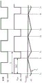
The invention will now be described by reference to the accompanying drawings, in which:
FIG. 1 illustrates an example apparatus architecture for generating an output voltage that tracks a reference voltage using a voltage control loop;
FIG. 2 illustrates an example device architecture for generating an output voltage that tracks a reference voltage using a voltage control loop and a current control loop;
FIG. 3 shows an exemplary schematic diagram of the architecture of FIG. 2;
4(a) -4 (c) illustrate example signals in the example implementation of FIG. 3;
FIG. 5 illustrates an improvement over the example implementation of FIG. 3;
6(a) -6 (e) illustrate example signals in the example implementation of FIG. 5;
FIG. 7 illustrates an improvement to the example implementation of FIG. 5;
FIG. 8 illustrates an improvement over the example implementation of FIG. 7;
9(a) through 9(e) illustrate example signals in the example implementation of FIG. 8;
FIG. 10 illustrates an example implementation in an envelope tracking scenario;
FIG. 11(a) shows an example implementation of a voltage-dropping regulator; and
fig. 11(b) and 11(c) show example implementations of a voltage boost regulator.
Detailed Description
Examples are described in which a switching power supply stage is controlled to generate an output voltage that tracks an input reference voltage. In described examples, a switching power supply stage includes a power stage including a pair of switches: a power switch connected between the switch node and a supply voltage, and a ground switch connected between the switch node and electrical ground. In an example, the supply voltage is a DC voltage, an example of which is a battery voltage. Other arrangements of switching stages may be used, but for descriptive purposes such an arrangement of a pair of switches is used.
Such a switching supply stage may be used to provide a switching supply voltage in an envelope tracking supply stage to a power amplifier. The envelope signal may be formed based on an input signal to be amplified, and the envelope signal provides a reference signal or reference voltage to the switching power supply stage. The switching power supply stage is used to generate an output voltage that provides a tracking power supply to the amplifier, which tracks a reference voltage provided by the envelope signal.
Amplifiers powered via switching power supply stages may be used to amplify signals in Radio Frequency Front End (RFFE) circuits. The RFFE circuitry may be used to facilitate transmission and reception of signals in the mobile device. In some cases, an amplifier may be used to amplify a Radio Frequency (RF) signal prior to transmission via one or more antennas. In this case, the envelope signal generated via the switching power supply stage may be generated based on the RF signal and used to power the amplifier.
An exemplary application is therefore to provide an envelope tracking power supply for an amplifier, but this is not a limiting application. Other applications may be to provide a fixed DC power supply for logic devices such as processors, input/output devices, memory, etc.
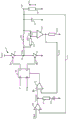
FIG. 3 illustrates an example implementation of the architecture of FIG. 2. In case the elements shown correspond to elements of a previous figure, the same reference numerals are used.
In the example implementation of fig. 3, a D-type flip-flop register 74 is provided. Other types of flip-flops may be used, and a D-type register is just one example. A switching stage 4 comprising switches 4 and 8 is also provided, and also an inductor 10, a capacitor 12 and a load 14. An amplifier 72, a resistor 97, a capacitor 99 and a compensation amplifier 95 are additionally provided.
As shown in fig. 3, D-type flip-flop register 74 receives a high voltage at the data input, denoted D, on line 80. The D input of the flip-flop is thus held at a "1" level. The clock input of the D flip-flop receives a clock signal on line 82. The clear/reset input of the D-type flip-flop receives the output of amplifier 72 on line 84. The Q and Qbar outputs of the D-type flip-flop register 74 provide control signals on lines 76 and 78 to control the respective switches 6 and 8 of the switching stage 4 to generate the signal V at the switching node 18SW。
The compensation amplifier 95 receives a reference voltage V on line 24REFAnd receives a feedback output voltage V on line 71OOr receiving a feedback output voltage VOIs shown. The compensation amplifier 95 is a differential amplifier and is derived from a reference voltage VREFMinus the output voltage VOAnd generates an amplified difference as the compensation voltage V on line 86COMP。
The compensation amplifier 95 is a voltage-current amplifier, and a resistor 97 and a capacitor 99 are provided at the output of the amplifier 95 to generate a compensation voltage VCOMP. Resistor 97 and capacitor 99 form a compensation function with amplifier 95 such that the compensation voltage VCOMPIs a function of the error between the output voltage and the reference voltage (the difference between the required value and the value actually present at the output).
Compensation voltage V on line 86COMPProvided as one input to amplifier 72. The other input to amplifier 72 is the current I on line 70 flowing from the inductorLThe detection of (2) is fed back to the signal. Amplifier 72 is a differential amplifier and subtracts a voltage representative of the current flowing in inductor 10 from the compensation voltage and generates a control signal to the clear/reset input of the D-type flip-flop accordingly. This operation can also be performed in the current domain instead of the voltage domain (the amplifier compares two currents instead of two voltages).
As mentioned above, the output voltage VOFormed across the load at the output node.
Thus, an indication of the error between the output voltage and the reference voltage is generated, and then an indication of the error between the signal and the representation of the current flowing in the inductor is generated.
The current control stage shown in fig. 3 suffers from sub-harmonic instability. These instabilities can occur when the duty cycle of the converter is higher than 50% for maximum current control and lower than 50% for minimum current control. This reduces the output range of the current controlled buck converter and makes such a control scheme unsuitable for many applications.
Fig. 4(a) to 4(c) illustrate the operation of the implementation of fig. 3.
Fig. 4(a) shows the clock signal at the clock input to the D-type flip-flop 74. The clock signal is obtained from any kind of oscillator. It is generated externally and the duty cycle is not important for a D-type flip-flop. The clock period being from t1To t3Of the time period T.
FIG. 4(b) shows the voltage V at the switch node 18SW. Signal at switch node is at VBATTo 0V (electrical ground). The clock period is T and the switching node is at VBATThe pulse width of time is DxT. Thus, the signal at the switching node is from time t1To time t2At VBAT(duration DxT) and from time t2To time t3Is 0V.
FIG. 4(c) shows the detected inductor current IL. As shown, the signal is a ramp signal, which is at V at the switch nodeBATRises and falls when the switch node is 0V. Thus, from time t1Switch 6 is closed and switch 8 is open and represents the inductor current ILThe signal of (2) rises. At time t2This signal is equal to the compensation voltage (detected by amplifier 72) and register 74 is controlled to open switch 6 and close switch 8. Thus, from time t2The signal representing the inductor current is ramped down to ramp down at time t3(at the end of the clock cycle) ramps down to zero.
Also shown in FIG. 4(c) is signal VCOMPA signal based on the inductor current and the signal VCOMPAnd (6) comparing. Signal VCOMPIs a falling signal and as a result of the comparison of amplifier 72, whenever the ramp current meets level VCOMPThe ramp current signal switches from rising to falling due to the state change of switches 6 and 8.
It should be understood in fig. 4(c) that the ramp signal is representative of the current I in the inductor 10LThe voltage signal of (2).
Referring to FIG. 4(c), the current I in the inductor is shownLIs raised with a compensation voltage VCOMPAnd (6) comparing. When the signal is lower than VCOMPThe input on line 84 is held so that the input to register 74 is "clear". When the signal becomes equal to VCOMPThe output of amplifier 72 switches so that the register is reset and switches 6, 8 are controlled to connect inductor 10 to ground. Thus, the signal representing the inductor falls. At the beginning of the next clock cycle, the register 74 controls the switches to ramp up the inductor current.
The timing diagram of fig. 4 shows three clock cycles. Time t1、t3And t5Indicates the start of each clock cycle, and time t3、t5And t7Indicating the end of each clock cycle. Time t2、t4And t6Indicating the time at which the switches 4, 6 switch state within each of the three time periods shown.
There are instabilities associated with the circuit of fig. 3, and to address these instabilities, the modified circuit arrangement of fig. 5 is proposed. Fig. 5 shows a modification to the circuit arrangement of fig. 3. In case the elements of fig. 5 correspond to the elements of fig. 3, the same reference numerals are used.
Figure 5 shows the introduction of slope compensation in the arrangement of figure 3.
Compensation voltage VCOMPIt may be higher but this does not change the duty cycle.
The circuit of fig. 3 is modified such that the voltage V isINDIs provided on line 94 and is fed into one input of combiner 92, the voltage VINDRepresenting the detected current I flowing in the inductorL. The output of the combiner 92 is provided to an amplifier 72, which amplifier 72 generates an input to the clear/reset input of the D-type flip-flop 74 as previously described.
Ramp signal VCLIs provided on line 96 as a second input from ramp generation block 97 to combiner 92. The ramp may be a constant current charge of: a capacitor (condensor), or a transistor that tracks the internal slope of a reference oscillator, an operational amplifier that functions as an integrator, etc. The combiner 92 combines its two inputs to provide a signal to the amplifier 72.
The operation of the circuit of fig. 5 is further explained with reference to the waveforms shown in fig. 6.
Fig. 6(a) to 6(e) illustrate the operation of the implementation of fig. 5.
FIG. 6(a) shows the clock signal at the clock input to the D-type flip-flop. The clock signal is obtained from any kind of oscillator. The clock signal is also generated externally and the duty cycle is not important. The clock cycle being from time t1To time t2Of the time period T.
FIG. 6(b) shows the voltage V at the switch node 18SW. Signal at switch node is at VBATTo 0V (electrical ground). The clock period is T and the switching node is at VBATThe pulse width at time DxT. Thus, the signal at the switching noise is from time t1To time t2At VBATT(duration DxT) and from time t2To time t3Is 0V.
FIG. 6(c) shows the measured voltage signal VINDIndicated, detected inductor current ILIs shown. As shown, the signal is a ramp signal, which is at V at the switch nodeBATRises and falls when the switch node is 0V. From time t1Switch 6 is closed and switch 8 is open and represents the inductor current ILThe signal of (2) rises. At time t2This signal is equal to the compensation voltage (detected by amplifier 72) and register 74 is controlled to open switch 6 and close switch 8. Thus, from time t2The signal representing the inductor current ramps down, at time t3(at the end of the clock cycle) ramps down to zero.
FIG. 6(d) shows the ramp signal, signal V, generated by ramp generator 97 on line 96CL. The ramp signal has a ramp-up portion throughout the clock cycle and is zero at the end of the clock cycle and rises again. Thus, the ramp is at time t1Ramp up from zero and at time t3Reset to zero.
Fig. 6(e) shows the signal at the output of the combiner 92, i.e. the signal on lines 94 and 96 or the combination of the signals of fig. 6(c) and 6 (d).
As shown in FIG. 6(e), the signal is from time t1The ramp is raised. At time t2The signal becomes equal to the compensation signal VCOMPAnd switch 6 is open and switch 6 is closed. Thus, from time t2To at time t3The inductor 10 discharges and the ramp decreases. The falling ramp is a combination of the falling ramp of fig. 6(c) and the rising ramp of fig. 6(d) during this period. At time t3The signal at the input of amplifier 72 is reset to zero.
Also shown in FIG. 6(e) is signal VCOMPA signal based on the inductor current and the signal VCOMPAnd (6) comparing. Signal VCOMPIs shown as a falling signal, but is actually a varying signal that varies up and down, and as a result of the comparison of amplifier 72, whenever the representation of the ramp current meets level VCOMPThe ramp current signal switches from rising to falling. Register 72 is then reset and the inductor discharges to the end of the clock cycle. At the end of the clock cycle, the signal is reset and begins to ramp up again.
Thus, the signal V at the input of the comparison amplifier 72CL+VINDRises until it equals the signal V on line 86COMPThereafter the set/clear signal to flip-flop 74 is changed by the comparison amplifier 72 and the current in the inductor is thus reduced.
Thus, an additional stage is provided which comprises combining the measured current flowing in the inductor with a ramp and feeding the combined signal to the input of the comparison amplifier.
This slope compensation overcomes the problem of subharmonic instability. The slope is added to the sensed current by combiner 92 and stabilizes the converter. The added slope may be proportional to the output voltage to achieve continuous suppression of sub-harmonic problems. However, the implementation of the variable slope compensation circuit is difficult and requires several operational amplifiers, adders, etc. This increases power consumption and silicon area.
In order to implement the circuit arrangement of fig. 5, the current flowing in the inductor has to be measured. For this purpose a series connected resistor capacitor (R/C) network may be used, which is connected in parallel with the coils shown in fig. 7. Any elements in fig. 7 that correspond to elements of the previous figures are denoted by the same reference numerals.
By arranging a resistor and a capacitor connected in series in parallel with the inductance, a measurement of the current flowing in the inductor can be obtained.
As shown in fig. 7, capacitor 102 is connected to output node 19, and resistor 100 is connected to switch node 18, and capacitor 100 and resistor 102 are connected together. Capacitors and resistors 102 and 100 are connected in series across inductor 10.
A small transconductance amplifier 104 (or differential amplifier) is connected to measure the current flowing in the inductor. The input of transconductance amplifier 104 is connected across capacitor 102 of resistor-capacitor connection 100-102. A first input branch of amplifier 104 is connected to the interconnection of resistor 100 and capacitor 102, and a second input branch of amplifier 104 is connected to output node 19.
The output of transconductance amplifier 104 is connected to one terminal of resistor 106, and the other terminal of resistor 106 is connected to electrical ground. Thus, a voltage representative of the current flowing in the capacitor 102 is formed at the output of the amplifier 104.
Thus, a measurement of the current flowing in inductor 10 is provided at the output of transconductance amplifier 104 on line 116. The voltage at the output of transconductance amplifier 104 is proportional to the current in inductor 10.
The voltage generated across its output load 106 at the output of transconductance amplifier 104 may then be used to provide a voltage indicative of the current flowing in inductor 10. Thus, the voltage developed at the output of transconductance amplifier 104 may be provided to amplifier 72, which forms the input to the D-type flip-flop.
Thus, the arrangement of fig. 7 provides for an inductor current to be sensed according to the implementation of fig. 3. To further modify fig. 7 to implement the arrangement of fig. 5, additional circuitry is required to process the output signal of transconductance amplifier 104 before it is provided to amplifier 72. This circuit requires a large number of components.
Fig. 8 shows a modification that avoids the need for such a large circuit. In fig. 8, a further small capacitor 110, a further resistor 112 and a switch 114 are added to the arrangement of fig. 7 in order to achieve operation consistent with fig. 5 and fig. 6(a) to (e). Any elements in fig. 8 that correspond to elements of the previous figures are denoted by the same reference numerals.
The resistor 100 and capacitor 102 are respectively noted as RFAnd CFAnd the resistor 112 and capacitor 110 are respectively noted as RSLAnd CSL。
A further small capacitor 110 is connected between the output node 19 and a further resistor 112, the other terminal of the further resistor 112 being connected to electrical ground. As previously mentioned, the interconnection from the resistor 100 and the capacitor 102 is provided to the first input branch of the amplifier. A second input branch to the transconductance amplifier 104 is provided by the connection point of the further capacitor 102 and the further resistor 100.
A switch 114 is arranged in parallel with the further capacitor 110.
The output of the transconductance amplifier 104 is connected to a comparison amplifier 72, the comparison amplifier 72 providing a clear/reset input to a D-type flip-flop 74.
The voltage across the capacitor 102 is proportional to the output current at the beginning of the cycle. Amplifier 104 adds current information plus the slope from switched capacitor 110. The switched capacitor provides a slope when the switch 114 is open. The slope depends only on the output voltage. When the slope is proportional to the output voltage, optimal slope compensation is achieved. If the output voltage is low, the slope is low. If the output voltage is high, the slope is high.
This operation is consistent with the generation of the ramp compensated signal according to fig. 6 (e).
By matching the resistance values of resistors 100 and 112, and by matching the capacitance values of capacitors 102 and 110, control is achieved to enable adjustment of the slope compensation ratio by simply adjusting the passive component matching ratio.
The switch 114 is controlled by a control signal 78, which control signal 78 controls the grounding switch 8 of the switching stage, so that when the grounding switch 8 is open, the switch 114 is open. Therefore, when the power switch 6 is closed, the switch 114 is opened.
The slope of the ramp signal is the slope of the signal in capacitor 102 (proportional to the coil current) plus the slope of the signal in capacitor 110 (proportional to the output voltage).
When ground switch 8 is closed, switch 1114 is closed. This discharges the slope compensation circuit and the slope is proportional to the coil current.
Fig. 9(a) to 9(e) show the operation of the circuit of fig. 8.
Fig. 9(a) shows the clock signal at the input to the D-type flip-flop. The clock signal is derived from any kind of oscillator. The clock signal is also generated externally and the duty cycle is not important for a D-type flip-flop. The clock cycle being from time t1To time t2Of the time period T.
FIG. 9(b) shows the voltage V at the switch node 18SW. Signal at switch node is at VBATTo 0V (electrical ground). The clock period is T and the switching node is at VBATThe pulse width at time DxT. Thus, the signal at the switching node is at time t1To time t2At VBAT(duration DxT) and at slave time t2To time t3Is 0V.
FIG. 9(c) shows the detected inductor current ILRepresented by the voltage present on the first input to amplifier 104. This is a signal generated due to detection at a node to which the resistor 100 and the capacitor 102 are commonly connected. As shown, the signal is a ramp signal, which is at V at the switch nodeBATRises and falls when the switch node is 0V. From time t1Switch 6 is closed and switch 8 is open and represents the inductor current ILThe signal of (2) rises. At time t2The signal is equal to the compensation voltage (detected by amplifier 72) and is transmittedThe latch 74 is controlled to open the switch 6 and close the switch 8. Thus, from time t2The signal of the inductor represents a fall, at time t3(at the end of the clock cycle) ramps down to zero.
Fig. 9(d) shows the ramp signal generated for the second input to amplifier 104. As shown, when switch 114 is open (and switch 8 is open, and switch 6 is closed), a ramp signal is generated on the signal line. The ramp signal has a gradient determined by the time constant of the resistor 100 and capacitor 102 combination and the resistor 112 and capacitor 110 combination.
When switch 8 is closed (and switch 6 is open), switch 114 is closed. No ramp signal is generated to the second input of amplifier 104.
Thus, there is a signal that is a ramp signal that ramps up when switch 6 is closed and is zero volts when switch 8 is closed.
From time t1The signal is ramped up to time t2. At time t2The ramp up terminates and the signal is reset to zero and remains at zero until time t3. Time t2Is the time at which switches 6 and 8 change state and represents the time at which switch 114 is closed.
The signal being derived from time t1Ramp up to time t2. This ramp is a combination of the ramp up of the signals of both fig. 9(c) and 9 (d). At time t2As the ramp of fig. 9(d) falls to zero, the signal falls by a certain level. From time t2To time t3This signal of (a) of fig. 9, which is a falling ramp.
Fig. 9(e) shows the signal generated at the output of amplifier 104, which is the sum of the signals at its two inputs, i.e. the sum of the signals in fig. 9(c) and 9 (d).
Thus, an additional stage is provided which comprises measuring the current flowing in the inductor and combining this current with the ramp and feeding the combined signal to the input of the comparison amplifier.
Referring to fig. 10, an application of the above principles in an envelope tracking implementation is shown. In the case where elements correspond to elements in the foregoing drawings, the same reference numerals are used.
As shown in fig. 10, a linear amplifier 166, a capacitor 162, a comparator 164, and an RF (radio frequency) power amplifier 152 are provided.
The RF power amplifier 152 receives an RF input signal on line 156 and generates an RF output signal on line 158. The RF output signal on line 158 is connected to an antenna 160.
Output voltage VOThe supply voltage on line 154 is provided to the RF power amplifier 152.
The envelope of the RF input signal on line 156 is provided on line 168 to the input of a linear amplifier 166. The output of the linear amplifier 166 on line 170 is connected to one terminal of the capacitor 162. The other terminal of the capacitor 162 is connected to the output voltage VO. Output voltage VOConnected to the second terminal of the inductor 10, the first terminal of the inductor 10 being connected to the switching voltage VSW。
The switcher block 150 represents the register 74 and switches 6 and 8 in the arrangement of figure 8. Thus, the switch block 150 receives the output of the amplifier 72 and generates the switching voltage VSW。
A voltage V is developed across capacitor 162CAPAnd this resulting voltage is detected by comparator 164, which comparator 164 generates a representation of the voltage across the capacitor on line 172.
Reference voltage VREFRepresenting a desired voltage to be established across capacitor 162 such that the compensation voltage VCOMPRepresenting the difference between the desired voltage and the actual voltage across capacitor 162.
In the foregoing description, the step-down circuit has been implemented. Using the described techniques, a boost circuit may also be provided.
Referring to fig. 11(a), a buck control circuit according to the principles described above is shown. Where elements corresponding to elements of previous figures are shown, the same reference numerals are used.
The supply voltage being defined by the battery voltage VBATOne terminal of switch 6 is provided on line 202. A capacitor 200 is connected between the electrical ground and the terminal of the switch 6 to supply a voltage VBAT。
The other terminal of the switch 6 is connected to one terminal of the switch 8, and the other terminal of the switch 8 is connected to electrical ground. The switches 6 and 8 are connected by a switcher control block 202, which switcher control block 202 can control the switcher according to the arrangement described above. The input of the switcher control block 202 is provided by the amplifier 104. The amplifier 104, capacitors 102, 112 and resistors 100, 110 are connected as described above. A switch 114 is also shown.
The switch control block 202 controls the switching stages included on the switches 6 and 8 according to a signal from the output of the amplifier 104, which is a slope-compensated feedback signal. According to the above, the ramp compensation is generated from the output of the buck stage.
The arrangement of fig. 11(a) is a buck stage according to the above arrangement. A boost stage may also be provided.
Referring to fig. 11(b), the arrangement of fig. 11(a) is modified to provide a boost circuit. The connection of the resistor 112 is adjusted so that the second terminal of the resistor 112 is connected to the first terminal of the switch 6, instead of being electrically grounded. The capacitor 12 is replaced by a capacitor 204 which provides the power supply (battery) voltage. An output voltage is then developed across capacitor 200.
Fig. 11(c) shows a rearrangement of the circuit of fig. 11(b) in which the capacitor 204 is disposed on the left-hand side and the capacitor 200 is disposed on the right-hand side.
Fig. 11(a) is a circuit for providing shape compensation in a buck converter to give a regulated buck. Fig. 11(c) is a circuit that provides shape compensation in a boost converter to provide a regulated boost.
The invention has been described with reference to specific examples, but the invention is not limited to details of any example, nor to details of an example used only in combination with other details. The various aspects of the examples may be used with the present invention, alone or in combination.
Claims (19)
1. A voltage regulator, comprising:
a switching stage;
an inductive element coupled between the switching stage and an output of the voltage regulator; and
a feedback path coupled to the switching stage, wherein the feedback path comprises:
an amplifier;
a first resistive element having a first terminal coupled to a first terminal of the inductive element;
a first capacitive element having a first terminal coupled to the second terminal of the inductive element, a second terminal of the first resistive element and a second terminal of the first capacitive element coupled to the first input of the amplifier; and
a switch coupled between a second input of the amplifier and the second terminal of the inductive element.
2. The voltage regulator of claim 1, wherein a feedback signal is generated by the feedback path to control the switching stage, the feedback signal being generated by applying a ramp compensation to a signal representative of a current flowing to the output of the voltage regulator.
3. The voltage regulator of claim 2, wherein the representation representative of current flowing to the output of the voltage regulator is generated by measuring a voltage difference across the first capacitive element.
4. The voltage regulator of claim 1, further comprising:
a second capacitive element having a first terminal connected to the second terminal of the inductive element; and
a second resistive element having a first terminal connected to a second terminal of the second capacitive element.
5. The voltage regulator according to claim 4, wherein the second input of the amplifier is connected to another connection point between the second capacitive element and the second resistive element, the output of the amplifier being connected to a control input of the switching stage.
6. The voltage regulator of claim 5, wherein:
the switch is connected in parallel with the second capacitive element;
when the switch is closed, the amplifier is configured to generate a feedback signal at the output of the amplifier, the feedback signal being representative of a current flowing across the inductive element; and is
When the switch is open, the amplifier is configured to generate a ramp compensated feedback signal at the output of the amplifier.
7. The voltage regulator of claim 6, wherein the switch is closed when the first terminal of the inductive element is connected to electrical ground via the switching stage, and the switch is open when the first terminal of the inductive element is connected to a voltage rail via the switching stage.
8. The voltage regulator of any of claims 1 to 7, further comprising:
a first comparator configured to compare an output voltage of the voltage regulator with a reference voltage to provide a comparison voltage; and
a second comparator configured to compare the comparison voltage with a feedback signal generated by the feedback path and to provide a control signal for the switching stage based on the comparison of the comparison voltage with the feedback signal.
9. The voltage regulator of claim 8, further comprising:
a linear amplifier; and
a power amplifier configured to receive a signal to be amplified and the linear amplifier configured to receive an envelope of the signal to be amplified;
a third capacitive element connected between an output of the linear amplifier and the second terminal of the inductive element, wherein the second terminal of the inductive element is connected to a power supply input of the power amplifier; and
a third comparator connected in parallel with the third capacitive element and having an output connected to the first comparator, wherein the reference voltage is indicative of a desired voltage to be formed across the third capacitive element.
10. The voltage regulator of claim 4, wherein a second terminal of the second resistive element is connected to electrical ground.
11. A method for voltage regulation, comprising:
generating a first signal representative of a current flowing to an output of a voltage regulator and a second signal having a slope based on an output voltage of the voltage regulator;
generating a feedback signal based on the first signal and the second signal; and
controlling a switching stage of the voltage regulator with the feedback signal to generate the output voltage.
12. The method of claim 11, wherein the voltage regulator comprises:
an inductive element having a first terminal connected to the switching stage and a second terminal connected to the output of the voltage regulator;
a first resistive element having a first terminal connected to the first terminal of the inductive element; and
a first capacitive element having a first terminal coupled to the second terminal of the first inductive element, a second terminal of the first resistive element and a second terminal of the first capacitive element coupled together, the first signal generated at the second terminal of the first capacitive element.
13. The method of claim 12, wherein the voltage regulator further comprises:
a second capacitive element having a first terminal connected to the second terminal of the inductive element; and
a second resistive element having a first terminal connected to a second terminal of the second capacitive element, the method further comprising generating the second signal via the second capacitive element and the second resistive element.
14. The method of claim 13, wherein the voltage regulator further comprises:
a feedback comparator, a first input of the feedback comparator connected to a connection point between the first resistive element and the first capacitive element, the method further comprising providing the second signal to a second input of the feedback comparator, the feedback signal generated at an output of the feedback comparator.
15. The method of claim 14, further comprising:
closing a switch connected in parallel with the second capacitive element to generate a further feedback signal representative of a current flowing to the output of the voltage regulator, the switching stage being controlled via the further feedback signal when the switch is closed; and
opening the switch connected in parallel with the second capacitive element to generate the feedback signal, the switching stage being controlled via the feedback signal when the switch is open.
16. The method of claim 15, wherein the switch is closed when the first terminal of the inductive element is connected to electrical ground and the switch is open when the first terminal of the inductive element is connected to a voltage rail.
17. The method of any of claims 12 to 16, further comprising:
comparing the output voltage to a reference voltage to provide a comparison voltage; and
comparing the comparison voltage with the feedback signal; and
providing a control input to the switching stage based on the comparison of the comparison voltage and the feedback signal.
18. The method of claim 17, further comprising:
receiving a signal to be amplified at an input of a power amplifier; and
receiving an envelope of the signal to be amplified at an input of a linear amplifier; wherein:
the voltage regulator comprising a third capacitive element connected between an output of the linear amplifier and the second terminal of the inductive element, wherein the second terminal of the inductive element is connected to a power supply input of the power amplifier,
the method further comprises detecting a voltage across the third capacitive element; and is
The comparison of the output voltage to the reference voltage includes comparing the detected voltage across the third capacitive element to the reference voltage, the reference voltage being indicative of a desired voltage to be formed across the third capacitive element.
19. The method of claim 13, wherein a second terminal of the second resistive element is connected to electrical ground.
Applications Claiming Priority (3)
| Application Number | Priority Date | Filing Date | Title |
|---|---|---|---|
| GB1509204.2 | 2015-05-28 | ||
| GB1509204.2A GB2538782A (en) | 2015-05-28 | 2015-05-28 | Improved tracking |
| PCT/US2016/034361 WO2016191570A1 (en) | 2015-05-28 | 2016-05-26 | Improved tracking |
Publications (2)
| Publication Number | Publication Date |
|---|---|
| CN107667463A CN107667463A (en) | 2018-02-06 |
| CN107667463B true CN107667463B (en) | 2020-07-28 |
Family
ID=53677373
Family Applications (1)
| Application Number | Title | Priority Date | Filing Date |
|---|---|---|---|
| CN201680030756.8A Active CN107667463B (en) | 2015-05-28 | 2016-05-26 | Voltage regulator and method for voltage regulation |
Country Status (6)
| Country | Link |
|---|---|
| US (1) | US10164525B2 (en) |
| EP (1) | EP3304715A1 (en) |
| JP (1) | JP2018516524A (en) |
| CN (1) | CN107667463B (en) |
| GB (1) | GB2538782A (en) |
| WO (1) | WO2016191570A1 (en) |
Families Citing this family (5)
| Publication number | Priority date | Publication date | Assignee | Title |
|---|---|---|---|---|
| DE102016012352A1 (en) * | 2016-10-14 | 2018-04-19 | Leopold Kostal Gmbh & Co. Kg | Buck-boost switching converter |
| US10122280B1 (en) * | 2017-12-26 | 2018-11-06 | Texas Instruments Incorporated | Loop control coefficients in a buck converter |
| US10770961B2 (en) * | 2018-04-16 | 2020-09-08 | M3 Technology Inc. | Power converter with adjustable ramp |
| EP3667886B1 (en) * | 2018-12-10 | 2021-12-08 | MediaTek Singapore Pte Ltd | Dc-dc converter having higher stability and output accuracy |
| WO2024030722A1 (en) * | 2022-08-05 | 2024-02-08 | Psemi Corporation | Multi-mode power converters with shared components |
Citations (5)
| Publication number | Priority date | Publication date | Assignee | Title |
|---|---|---|---|---|
| US4975820A (en) * | 1989-09-01 | 1990-12-04 | National Semiconductor Corporation | Adaptive compensating ramp generator for current-mode DC/DC converters |
| CN102035384A (en) * | 2010-12-13 | 2011-04-27 | 成都芯源系统有限公司 | Switching converter circuit and power conversion method |
| GB2510396A (en) * | 2013-02-01 | 2014-08-06 | Nujira Ltd | Controlling resonance in an envelope tracking power supply |
| CN104022648A (en) * | 2014-04-23 | 2014-09-03 | 成都芯源系统有限公司 | Switch converter and control circuit and control method thereof |
| CN104335469A (en) * | 2012-06-08 | 2015-02-04 | 瑞典爱立信有限公司 | Controlling a switched mode power supply with maximised power efficiency |
Family Cites Families (12)
| Publication number | Priority date | Publication date | Assignee | Title |
|---|---|---|---|---|
| US4837495A (en) * | 1987-10-13 | 1989-06-06 | Astec U.S.A. (Hk) Limited | Current mode converter with controlled slope compensation |
| US5982160A (en) * | 1998-12-24 | 1999-11-09 | Harris Corporation | DC-to-DC converter with inductor current sensing and related methods |
| US6812677B2 (en) * | 2001-08-21 | 2004-11-02 | Intersil Americas Inc. | Thermally compensated current sensing of intrinsic power converter elements |
| US6441597B1 (en) * | 2001-10-31 | 2002-08-27 | Semtech Corporation | Method and apparatus for sensing output inductor current in a DC-to-DC power converter |
| JP4364554B2 (en) * | 2002-06-07 | 2009-11-18 | 株式会社ルネサステクノロジ | Switching power supply device and switching power supply system |
| TWI355498B (en) * | 2007-11-19 | 2012-01-01 | Inventec Corp | Power measuring apparatus |
| TWI479780B (en) * | 2010-12-13 | 2015-04-01 | Hon Hai Prec Ind Co Ltd | Synchronous buck converter |
| US8947061B2 (en) * | 2011-03-10 | 2015-02-03 | Broadcom Corporation | Hysteretic switching regulator with reduced switching frequency variation |
| US8698475B2 (en) * | 2011-10-20 | 2014-04-15 | Monolithic Power Systems, Inc. | Switching-mode power supply with ripple mode control and associated methods |
| US9041363B2 (en) | 2012-09-21 | 2015-05-26 | Analog Devices Global | Windowless H-bridge buck-boost switching converter |
| US9081403B1 (en) * | 2013-03-13 | 2015-07-14 | Maxim Integrated Products, Inc. | Optimal compensating ramp generator for fixed frequency current mode DC-DC converters |
| WO2016114911A1 (en) * | 2015-01-12 | 2016-07-21 | Hua Cao | Switching regulator and control method thereof |
-
2015
- 2015-05-28 GB GB1509204.2A patent/GB2538782A/en not_active Withdrawn
-
2016
- 2016-05-26 US US15/574,382 patent/US10164525B2/en active Active
- 2016-05-26 JP JP2017561294A patent/JP2018516524A/en active Pending
- 2016-05-26 EP EP16728500.6A patent/EP3304715A1/en not_active Withdrawn
- 2016-05-26 CN CN201680030756.8A patent/CN107667463B/en active Active
- 2016-05-26 WO PCT/US2016/034361 patent/WO2016191570A1/en active Application Filing
Patent Citations (5)
| Publication number | Priority date | Publication date | Assignee | Title |
|---|---|---|---|---|
| US4975820A (en) * | 1989-09-01 | 1990-12-04 | National Semiconductor Corporation | Adaptive compensating ramp generator for current-mode DC/DC converters |
| CN102035384A (en) * | 2010-12-13 | 2011-04-27 | 成都芯源系统有限公司 | Switching converter circuit and power conversion method |
| CN104335469A (en) * | 2012-06-08 | 2015-02-04 | 瑞典爱立信有限公司 | Controlling a switched mode power supply with maximised power efficiency |
| GB2510396A (en) * | 2013-02-01 | 2014-08-06 | Nujira Ltd | Controlling resonance in an envelope tracking power supply |
| CN104022648A (en) * | 2014-04-23 | 2014-09-03 | 成都芯源系统有限公司 | Switch converter and control circuit and control method thereof |
Also Published As
| Publication number | Publication date |
|---|---|
| GB201509204D0 (en) | 2015-07-15 |
| GB2538782A (en) | 2016-11-30 |
| WO2016191570A1 (en) | 2016-12-01 |
| CN107667463A (en) | 2018-02-06 |
| US20180145589A1 (en) | 2018-05-24 |
| US10164525B2 (en) | 2018-12-25 |
| EP3304715A1 (en) | 2018-04-11 |
| JP2018516524A (en) | 2018-06-21 |
Similar Documents
| Publication | Publication Date | Title |
|---|---|---|
| CN107667463B (en) | Voltage regulator and method for voltage regulation | |
| CN101828327B (en) | DC/DC converter arrangement and method for DC/DC conversion | |
| JP4931530B2 (en) | Power converter | |
| US11022636B2 (en) | Current sensor circuit | |
| EP0700146B1 (en) | Voltage multiplier with linear stabilized output voltage | |
| US9755515B2 (en) | Switching regulator current sensing circuits and methods | |
| US9397559B2 (en) | Switching regulator current mode feedback circuits and methods | |
| US10044267B1 (en) | Current emulation auto-calibration with peak-current servo | |
| US10587196B1 (en) | Constant on-time controller and buck regulator device using the same | |
| US20090267573A1 (en) | Power Supplies, Power Supply Controllers, And Power Supply Controlling Methods | |
| US10103720B2 (en) | Method and apparatus for a buck converter with pulse width modulation and pulse frequency modulation mode | |
| US20240063710A1 (en) | Dynamic signal slope compensation | |
| US6930526B1 (en) | Quasi-feedforward PWM modulator | |
| US8970192B2 (en) | Buck converter with comparator output signal modification circuit | |
| US8664923B2 (en) | Buck converter with hysteresis correction | |
| KR20100078322A (en) | Dc-dc converter | |
| US9166468B2 (en) | Voltage regulator circuit with soft-start function | |
| TWI523391B (en) | Mixed mode compensation circuit | |
| CN103840664A (en) | Constant-current control circuit, switching regulator, integrated circuit and constant-current control method | |
| TWI699640B (en) | Contstant on-time controller and buck regulator device using the same | |
| CN109417385B (en) | Small capacitance compensation network circuit | |
| KR101171597B1 (en) | Apparatus of detecting zero-inductor-current for switching type voltage converter | |
| CN112019045A (en) | Fixed open-time controller and buck converter device using the same | |
| CN106685416A (en) | Oscillation circuit device |
Legal Events
| Date | Code | Title | Description |
|---|---|---|---|
| PB01 | Publication | ||
| PB01 | Publication | ||
| SE01 | Entry into force of request for substantive examination | ||
| SE01 | Entry into force of request for substantive examination | ||
| GR01 | Patent grant | ||
| GR01 | Patent grant |