CN107077963B - Transmitter for inductive power transfer system - Google Patents
Transmitter for inductive power transfer system Download PDFInfo
- Publication number
- CN107077963B CN107077963B CN201580051926.6A CN201580051926A CN107077963B CN 107077963 B CN107077963 B CN 107077963B CN 201580051926 A CN201580051926 A CN 201580051926A CN 107077963 B CN107077963 B CN 107077963B
- Authority
- CN
- China
- Prior art keywords
- housing
- coils
- power transfer
- inductive power
- coil
- Prior art date
- Legal status (The legal status is an assumption and is not a legal conclusion. Google has not performed a legal analysis and makes no representation as to the accuracy of the status listed.)
- Active
Links
Images


Classifications
-
- H—ELECTRICITY
- H01—ELECTRIC ELEMENTS
- H01F—MAGNETS; INDUCTANCES; TRANSFORMERS; SELECTION OF MATERIALS FOR THEIR MAGNETIC PROPERTIES
- H01F38/00—Adaptations of transformers or inductances for specific applications or functions
- H01F38/14—Inductive couplings
-
- H—ELECTRICITY
- H01—ELECTRIC ELEMENTS
- H01F—MAGNETS; INDUCTANCES; TRANSFORMERS; SELECTION OF MATERIALS FOR THEIR MAGNETIC PROPERTIES
- H01F27/00—Details of transformers or inductances, in general
- H01F27/02—Casings
-
- H—ELECTRICITY
- H01—ELECTRIC ELEMENTS
- H01F—MAGNETS; INDUCTANCES; TRANSFORMERS; SELECTION OF MATERIALS FOR THEIR MAGNETIC PROPERTIES
- H01F27/00—Details of transformers or inductances, in general
- H01F27/28—Coils; Windings; Conductive connections
- H01F27/2823—Wires
-
- H—ELECTRICITY
- H02—GENERATION; CONVERSION OR DISTRIBUTION OF ELECTRIC POWER
- H02J—CIRCUIT ARRANGEMENTS OR SYSTEMS FOR SUPPLYING OR DISTRIBUTING ELECTRIC POWER; SYSTEMS FOR STORING ELECTRIC ENERGY
- H02J50/00—Circuit arrangements or systems for wireless supply or distribution of electric power
- H02J50/10—Circuit arrangements or systems for wireless supply or distribution of electric power using inductive coupling
- H02J50/12—Circuit arrangements or systems for wireless supply or distribution of electric power using inductive coupling of the resonant type
Abstract
An inductive power transfer transmitter includes a housing for receiving a device to be powered. The housing has one or more side walls and one or more coils for generating an alternating magnetic field within the housing. The density of the one or more coils varies with distance from the end of the one or more sidewalls.
Description
Technical Field
The present invention is in the field of Inductive Power Transfer (IPT) systems. More particularly, the present invention relates to a power transmitter having a novel configuration for use in such a system.
Background
IPT systems are well known areas of prior art (e.g. wireless charging of electric toothbrushes) and developing technology (e.g. wireless charging of handheld devices on "charging pads"). Typically, the primary side generates a time-varying magnetic field from a transmitting coil or coils. This magnetic field induces an alternating current in a suitable receiving coil, which can then be used to charge a battery or power a device or other load. In some cases, the transmitter coil or receiver coil may be connected with a capacitor to create a resonant circuit that may increase power throughput or efficiency at a corresponding resonant frequency.
A fundamental problem that must be overcome in IPT system design is ensuring efficient power transfer. One way to improve performance is to require precise alignment of the transmitter and receiver coils, such as is the case with wireless charging of a power toothbrush using a dedicated charging dock. However, the need for precise alignment undermines one of the key goals of some IPT systems, namely simple charging and powering of the device (with minimal user involvement).
Another type of IPT system is a charging (or powering) pad. Typically, these systems provide a surface configured to generate a magnetic field such that when a suitable device is placed on the surface, electrical energy is acquired by a suitable receiver coil arrangement inside the device. There are various known transmit coil configurations. In one example, a single coil is placed below the surface and coplanar with the surface. The coils can be small and therefore the receiver coils must still be reasonably well aligned for power transfer. Alternatively, the coil may be large, covering the entire area of the surface. In this case, one or more receivers may be placed anywhere on the surface. This gives more freedom to charge or power the device (i.e. the user only has to put the device anywhere on the mat). However, the magnetic field generated by this arrangement is not uniform and the magnetic field may be particularly weaker towards the centre of the coil. Thus, the receiver coils obtain different amounts of electrical energy depending on their position on the surface.
A third type of IPT system is a charging (or powering) enclosure. Typically, these systems provide a box with transmitter coils contained in the side walls and/or base of the box. The coils generate a magnetic field within the cartridge body such that when the device is placed within the cartridge body, electrical energy is obtained by a suitable receiver coil arrangement within the device. The coils may be coil arrays, or large coils, or a combination of both. However, the same disadvantages as the charging plate occur. That is, the field is not uniform throughout the volume, being particularly weaker towards the center. Therefore, even when the device is placed in the center of the housing, in order to ensure sufficient power transmission, the power on the primary side must be higher, which results in increased losses and reduced efficiency.
In all the above cases, it is known that a layer/core made of a high permeability material (such as ferrite) can be included in the transmitter or receiver to improve the transfer of energy over the magnetic field.
It is an object of the present invention to provide a transmitter which produces a magnetic field with improved power transfer characteristics, or to at least provide the public with a useful choice.
Disclosure of Invention
According to an exemplary embodiment, there is provided an inductive power transfer transmitter comprising: a housing for housing a device to be energized, having one or more side walls; one or more coils for generating an alternating magnetic field within the housing, the density of the one or more coils varying with distance from the end of the one or more side walls; and a drive circuit for driving the one or more coils.
According to another exemplary embodiment, there is provided an inductive power transfer transmitter comprising: a housing for receiving a device to be energized, having a base portion and one or more side walls projecting from the base portion; one or more coils for generating an alternating magnetic field within the housing, the density of the one or more coils initially decreasing with increasing distance from the base portion and then increasing with further increasing distance from the base portion; and a drive circuit for driving the one or more coils.
According to another exemplary embodiment, there is provided an inductive power transmitter comprising: one or more coils for generating an alternating magnetic field; a drive circuit for driving one or more coils; and one or more magnetically permeable layers associated with the one or more coils, wherein a combined thickness of the one or more magnetically permeable layers varies.
According to yet another exemplary embodiment, there is provided an inductive power transmitter comprising: one or more coils for generating an alternating magnetic field; a drive circuit for driving one or more coils; and one or more magnetically permeable layers associated with the one or more coils, wherein the magnetic permeability of the one or more magnetically permeable layers varies.
It is acknowledged that the term 'comprise' and variations thereof may, under varying jurisdictions, be attributed with either an exclusive or an inclusive meaning. For the purposes of this specification, unless otherwise indicated, these terms are intended to have an inclusive meaning-i.e., they will be taken to mean an inclusion of the listed components as directly referenced, and possibly other unspecified components or elements.
The reference to any prior art in this specification does not constitute an admission that such prior art forms part of the common general knowledge.
Drawings
The accompanying drawings, which are incorporated in and constitute a part of the specification, illustrate embodiments of the invention and, together with a general description of the invention given above, and the detailed description of the embodiments given below, serve to explain the principles of the invention.
Fig. 1 shows a view of a transmitter according to an embodiment of a first aspect of the present invention;
fig. 2 shows a view of a transmitter according to another embodiment of the first aspect of the invention shown in fig. 1;
FIG. 3 shows a cross-sectional view of the emitter shown in FIG. 1;
FIG. 4 shows a schematic diagram comparing magnetic field lines generated by two different emitters;
FIG. 5 shows a view of an emitter according to an embodiment of another aspect of the invention;
FIG. 6 shows a view of an emitter according to an embodiment of another aspect of the invention;
FIG. 7 shows a cross-sectional view of the emitter shown in FIG. 6;
FIG. 7a illustrates a cross-sectional view of a portion of an emitter according to an embodiment of the aspect illustrated in FIG. 6;
FIG. 8 shows a cross-sectional view of another embodiment of the emitter shown in FIG. 6;
FIG. 9 shows a schematic of magnetic field lines produced by the transmitter of FIG. 6;
FIG. 10 shows a cross-sectional view of an emitter according to another aspect of the invention;
FIG. 11 shows a schematic diagram comparing magnetic field lines produced by two different emitters;
FIG. 12 shows a cross-sectional view of an emitter according to another aspect of the invention;
FIG. 13 shows a schematic diagram comparing magnetic field lines produced by two different emitters;
FIG. 14 illustrates a cross-sectional view of an emitter according to another embodiment of the aspect of the invention illustrated in FIG. 12; and
fig. 15 shows a schematic diagram of a driving circuit for driving the emitter of an embodiment of the invention.
Detailed Description
Coil arrangement
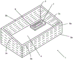
Referring to figure 1, there is shown a transmitter 1 for an IPT system according to an embodiment of the invention. The transmitter takes the form of a charging housing 2 with a side wall 3 and a base portion 4. The transmitter comprises a coil 5 which generates a time-varying magnetic field inside the housing. A device 6 placed within the housing includes a receiver coil 7 that is inductively coupled with the time-varying magnetic field and produces an electrical current that can be used to charge or power the device. The coil is contained by the side walls of the housing and is wound around the circumference of the housing coplanar with the base portion, as shown in phantom in fig. 1.
The transmitter 1 is connected to a suitable power supply 8 and a drive circuit (not shown) is configured to drive the coil such that it generates a magnetic field. The drive circuit is configured such that the coil 5 generates a time-varying magnetic field suitable for the specific application. Such driving circuits are known to those skilled in the art and the present invention is not limited in this respect.
Devices capable of receiving inductively transmitted electrical energy are well known in the art and the present invention is not limited to any particular type. In a preferred embodiment the device comprises a receiver coil coplanar with the base part, as this will maximise power transfer, with the magnetic flux of the magnetic field perpendicular to the base part.
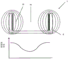
The shape of the housing 2 shown in fig. 1 takes the form of a rectangular prism, however the invention is not limited in this respect. Those skilled in the art will understand how to apply the present invention to defining various three-dimensional volumes of a housing. By way of example, fig. 2 shows an emitter 9 in which the housing is in the form of a cylinder with a single continuous side wall 10. In this example, the coil 11 is generally circular and is wound around the circumference of the housing, as shown by the dashed lines in fig. 2.
In a preferred embodiment of the invention, the housing comprises a base portion 4. As will be described later, the inclusion of a magnetically permeable layer (such as a ferrite layer) in the base portion can significantly improve the electrical energy transfer. However, the housing 2 does not necessarily include a base portion. Those skilled in the art will know how the present invention can be adapted to a charging housing that does not include a base portion.
Referring to fig. 3, a vertical cross-section of the emitter 1 shown in fig. 1 is shown. This view shows the side wall 3, the base part 4, the coil 5 and the device 6. The housing may optionally include a suitable outer layer 12 (e.g., a plastic shell), the outer layer 12 surrounding the inner working structure of the emitter, giving the emitter a more attractive and streamlined appearance. The coils are arranged such that the density of the coils (which is the number of loops per unit height) generally increases with height. This results in more rings being "concentrated" towards the top of the sidewall. The number of rings shown in fig. 3 is relatively small, as this is most useful for illustrating the principles of the present invention. In fact, the number of rings is not limited in any way, and those skilled in the art will appreciate that in certain applications the number of rings may be hundreds or even thousands.
Alternatively, in another embodiment of the invention, the coils may be configured such that the density varies in some other way with height. For example, consistent with the present invention, the density of the coils first increases with height and then decreases again toward the top of the sidewall. Such alternative embodiments are described later.
The coil 5 is continuous and connected in series to a drive circuit (not shown). In an embodiment of the invention, the coil comprises a single length of wire that is repeatedly wound to form a series of loops. In one embodiment of the invention, the single length of wire comprises multiple lengths of wire of different gauges. The lengths of wire may be joined together in a suitable manner (e.g., welding) such that the length of wire tapers from a maximum diameter to a narrowest diameter. Thus, if the wire is wound according to the coil configuration shown in fig. 3, the narrower section of the wire corresponds to a loop having a higher density. Because the wire is narrow, it occupies less space than if the wire had a consistent gauge. The wire may be any suitable current carrying wire including litz-type wires. Litz wire is advantageous because it greatly reduces the power loss caused by skin and proximity effects in conductors in IPT systems when operating at high frequencies. In another embodiment of the invention, there is more than one coil. Each coil may be connected in series, parallel, or other suitable form. In general, the net density of the coils (as the number of loops per unit height) may still vary according to the present invention.
The benefit of the invention can be seen in fig. 4a and 4b, which fig. 4a and 4b show a vertical cross section of a transmitter 1 according to an embodiment of the invention. Fig. 4a and 4b show a comparison between the magnetic field generated by a coil arrangement having a uniform density and the magnetic field generated by a coil arrangement according to the invention, respectively. It will be observed that for the former case in fig. 4a, the magnetic flux is concentrated towards the walls of the housing 13, wherein there is a region of lower magnetic flux towards the centre 14. Therefore, to ensure sufficient power transfer to a receiver placed in the central region, the power flow through the transmitter must be increased. This results in inefficient use of the power supply. Furthermore, receivers placed close to the side walls of the housing are subjected to a stronger magnetic field than receivers placed at the center. This requires the receivers to adjust their power flow according to their precise position within the housing. It also increases parasitic heating in the device. Fig. 4b shows the magnetic field of the coil arrangement according to the invention. As will be observed, the variable coil density results in a more uniform magnetic field throughout the housing. In effect, the additional winding causes the magnetic field to extend further into the housing. This helps to solve the problems caused by the non-uniform field described above. In particular, the power flow through the transmitter may be reduced while still ensuring sufficient power transfer to the receiver despite its placement inside the housing. Having reduced power flow in the transmitter minimizes inefficiencies and reduces parasitic heating. Those skilled in the art will understand that the fields shown in fig. 4b are qualitative in order to illustrate the principles of the present invention. In practice, the precise coil arrangement required to achieve the desired field characteristics depends on many variables, such as size and power rating. It will be appreciated that the design of the coil arrangement will need to be tailored to suit a particular application.
Returning to fig. 3, the ferrite layer 15 is also shown inside the side walls 3 and base portion 4 of the charging housing. Those skilled in the art will understand how the inclusion of a magnetically permeable layer can improve the performance of electrical energy transfer. In particular, the magnetically permeable layer in the base part "forces" the magnetic field lines to distribute closer to the center. This helps to provide a more uniform field and improves the transfer of electrical energy across the area of the substrate.
Referring to fig. 5, a transmitter 1 according to another aspect of the invention is shown. In this case, the transmitter is a charging housing 2a, which is similar to the charging housing 2 described above, however the charging housing 2a has an irregular shape instead of a rectangular prism shape as in the embodiment of fig. 1. That is, the housing includes side walls 3 and a base portion 4, with one side wall 3a having a different size than the opposite side wall 3b, so that the joining side wall 3c has an inclined upper surface. The terms upper and lower are used with respect to the base part 4. The actual shape of the housing 2a depends on the particular application of the transmitter, however it will be appreciated that the arrangement of magnetically permeable material and coils described herein in relation to the present invention is applicable where the housing is irregularly shaped.
As will be described later, the inclusion of a magnetically permeable layer (e.g., ferrite layer) in the base portion can significantly improve electrical energy transfer. However, similar to the embodiment of fig. 1, the housing 2a does not necessarily have to comprise a base portion. Those skilled in the art will understand how the present invention may be adapted to a charging housing that does not include a base portion.
The coil 5, which generates a time-varying magnetic field inside the housing 2a, is contained by the side walls of the housing and is wound around the circumference of the housing coplanar with the base portion, as shown by the dashed lines in fig. 5. The irregular shape of the housing 2a requires that the winding configuration of the coil 5 is adapted to the irregular shape while generating a magnetic field that substantially surrounds all of the interior of the housing in a substantially uniform manner. This is achieved by ensuring that the windings of the coil 5 are along the upper surface of the side wall portions 3a, 3b and 3c in at least the upper part of the housing 2a and by employing the above described density varying coil arrangement, as shown in fig. 5. Thus, a device 6 comprising a receiver coil 7 placed inside the housing 2a will be inductively coupled with the time-varying magnetic field to allow charging or powering of the device regardless of the relative positioning of the device inside the housing.
The transmitter 1 is connected to a suitable power supply and a drive circuit (not shown) is configured to drive the coil such that it generates a magnetic field. The drive circuit is configured such that the coil 5 generates a time-varying magnetic field suitable for the specific application. Such driving circuits are known to those skilled in the art and the present invention is not limited in this respect.
Further enhancement of the homogeneity of the magnetic field induced by the transmitter coil may be achieved using a coil arrangement as shown in fig. 6, fig. 6 showing the transmitter 1 of fig. 5. In fig. 6, the coil 5 is shown in solid lines to facilitate description. As can be seen, the winding configuration of the coil 5 is adapted as before to the irregular shape of the housing 2a, but a varying density arrangement (number of loops per unit height) is used which is different from the varying density arrangement described in the embodiment of fig. 1 and 5. That is, unlike the previous embodiment in which the density of the coil windings increases monotonically from the base portion 4 to the upper surface of the sidewall 3, the density of the coil windings in the embodiment of fig. 6 increases at both the lower and upper portions of the sidewall 3, and decreases at the middle portion of the sidewall. That is, the windings in the portion 5a at the upper part of the housing and the windings in the portion 5b at the lower part of the housing are denser than the windings in the portion 5c at the middle part of the housing. This results in more rings being "concentrated" towards the top and bottom of the sidewall. The number of rings shown in fig. 6 is relatively small, as this is most useful for illustrating the principles of the present invention. In fact, the number of rings is not limited in any way, and those skilled in the art will appreciate that in certain applications the number of rings may be hundreds or even thousands. The inventors have found that this alternative coil winding configuration provides even better homogeneity in the induced magnetic field. This configuration also allows for accommodation of irregularities in the shape, size and configuration of the housing while providing the required field inside the housing.
Referring to fig. 7, a vertical cross-section of the emitter 1 shown in fig. 6 is shown. This view shows the side wall 3, base portion 4, coil 5 and device 6 a. The housing may optionally include a suitable outer layer 12 (e.g., a plastic shell) that surrounds the inner working structure of the emitter. The outer layer 12 may be a shell for the emitter 1 itself, or may be part of a component of the vehicle interior or other infrastructure. The device 6a is shown as an arbitrarily shaped item rather than the generally rectangular item of the device shown in the previous figures. Any shape of the device 6a is used to illustrate the homogeneity of the magnetic field induced by the transmitter of various embodiments of the invention, such that efficient wireless or inductive power transfer is achieved independent of the shape of the receiver coil in the device and/or the relative orientation to the transmitter coil.
The coil 5 of fig. 5 and 6 may be continuous and connected to a drive circuit (not shown). In one embodiment, the coil is a single length of wire that is repeatedly wound to form a series of loops that are close together at coil portions 5a and 5b at the lower and upper portions of the sidewall, and farther apart at coil portion 5c at the middle portion of the sidewall, as shown in fig. 7. In another embodiment, the coil 5 may have multiple lengths of wire with different gauges, as shown in fig. 8. That is, section 5d at the highest and lowest portions of the sidewall is thicker than adjacent section 5e, and section 5e is thicker than section 5f at the middle portion of the sidewall. The lengths of wire may be connected together in a suitable manner (e.g., welding) such that the length of wire tapers from a maximum diameter to a narrowest diameter and back to the maximum diameter again above the height of the sidewall. The wire may be any suitable current carrying wire including litz-type wires. In another embodiment of the invention, there is more than one coil. Each coil may be connected in series, parallel, or other suitable form. In general, the net density of the coils (as the number of loops per unit height) may still vary according to the present invention.
With the coil configuration shown in fig. 7, the inventors have found that a particular number of loops or turns spaced between adjacent turns in the increased density portions 5a and 5b and a particular gradual change from the increased density portion to the decreased density portion provides an optimized operation for inducing a magnetic field. Fig. 7a shows an exemplary embodiment of a housing with irregularly configured emitters as shown in fig. 5 and 6, wherein the same reference numerals are used. In the example of fig. 7a, a 21-turn coil 5 is provided, wherein the coil density gradually increases from the base portion 4 of the housing 2a with increasing height to decreasing, wherein the gradual change depends on the local configuration of the housing 2 a. That is, as can be seen, the progression on the "higher" side of the housing is different from the progression on the "lower" side of the housing.
Specifically, in this example, the portion a of the coil 5 closest to the opening of the housing 2a on the lower sidewall 3a (e.g., the top of the charging "box," where the top is defined relative to the base portion) has a maximum coil density of ten turns, where adjacent turns of the coil are in contact with one another, i.e., there is substantially no space between adjacent turns, whereas the portion D of the coil 5 closest to the opening of the housing 2a on the upper sidewall 3b has a maximum coil density of seven turns, where adjacent turns of the coil are in contact with one another. On the lower side, this spacing between adjacent coil turns increases to about 1.0mm for one turn, while on the upper side, the spacing increases to about 1.0mm for two turns. The gradual change continues as the spacing between adjacent coil turns increases to about 3.0mm for one turn on both the low and high sides, and then to about 5.0mm for one turn on both sides.
In part B of the coil in the middle portion of the enclosed volume (e.g., the charging "cartridge") on the lower side, a minimum coil density of three turns is provided, with adjacent turns of the coil being spaced apart by about 6.0mm, while in part E of coil 5 in the middle portion on the upper side, a minimum coil density of five turns is provided, with adjacent turns of the coil being spaced apart by about 7.0 mm. The grading continues as the spacing between adjacent coil turns on both the low and high sides is reduced to about 5.0mm for one turn, then to about 3.0mm for one turn, and then to about 1.0mm for two turns. Finally, the portions C and F of the coil 5 which are closest to the base portion 4 of the case 2a on the lower side wall 3a and the upper side wall 3b, respectively, each have a maximum coil density of three turns, wherein adjacent turns of the coil are in contact with each other, i.e., there is substantially no space between the adjacent turns.
This configuration provides 20 specific spacings between adjacent turns for a total of 21 turns based on the distance from the base portion of the housing, with the spacing being from about 0.0mm to about 7.0 mm. As will be appreciated, the relevant spacing is spread out on the "angled" side of the housing, as shown in fig. 6, for example.
The benefits of this embodiment of the invention can be seen in fig. 9, which shows a vertical cross section of the transmitter 1 with the coil arrangement of fig. 8 and the magnetic field generated thereby. By comparing the magnetic field generated by the coil arrangement of figure 9 with that generated by the coil arrangement shown in figure 4a, it can be seen that unlike the example of figure 4a in which the magnetic flux is concentrated towards the walls of the housing 13 with a region of lower magnetic flux towards the centre 14, in the arrangement of the present embodiment the magnetic flux is more uniform throughout the interior of the housing 2 a. In effect, the additional winding causes the magnetic field to extend further into the housing. This helps solve the problem caused by the non-uniform field of fig. 4a discussed earlier. In particular, the power flow through the transmitter of the present invention may be reduced relative to that of fig. 4a, while still ensuring sufficient power transfer to the receiver despite its placement within the housing. Having reduced power flow in the transmitter minimizes inefficiencies and reduces parasitic heating. Those skilled in the art will appreciate that the magnetic fields shown in FIG. 9 are qualitative in order to illustrate the principles of the present invention. In practice, the precise coil arrangement required to achieve the desired field characteristics depends on many variables, such as size and power rating. It will be appreciated that the design of the coil arrangement will need to be tailored to suit a particular application.
Returning to fig. 7 and 8, there is also shown a magnetically permeable material element 15a inside the side wall 3 and base portion 4 of the charging housing 2 a. Those skilled in the art will understand how the inclusion of a magnetically permeable material, such as ferrite, can improve the performance of power transfer. In particular, suitable magnetically permeable materials "force" the magnetic field lines to be distributed closer to the center. This helps to provide a more uniform field and improved power transfer across the area of the substrate. It also blocks or shields the generation of (electric) magnetic fields outside the transmitter housing. This improves the safety of the transmitter and the compatibility of the use of the transmitter in environments with other electronic or metallic components, such as vehicle interiors. This shielding effect is enhanced by ensuring that there are no gaps between the elements 15a, as shown in fig. 7 and 8. Further enhancement may be provided by providing a further portion 15b of magnetically permeable material element, wherein the further portion 15b of magnetically permeable material element surrounds the transmitter coil 5 in the region of the upper surface of the side wall, as shown in fig. 8. A removable cover of or with magnetically permeable material may also be provided. Effective shielding is also provided by the configuration of the element 15 in the embodiment of fig. 3 and the embodiments described later. It should be noted that certain applications of the transmitter may require a gap in the housing, wherein the magnetically permeable material element forms part of the housing in order to accommodate the shape/configuration of the housing and the power supply connection (such as connection 8 in fig. 1). In any application where a gap may be avoided or required, the magnetically permeable material elements may be formed as a single unit, rather than as separate elements, by molding or other techniques known to those skilled in the art.
The charging/powering housing described above need not be a stand-alone device, but may be incorporated into a pre-existing structure or a specially designed structure. As an example, a desk drawer may be constructed in accordance with the present invention so that a user will only need to place their electronic device in the drawer, which can be recharged or powered. In another example, a console or other similar component inside a vehicle may be configured to include a transmitter housing in accordance with the present invention, so a user would only need to place their electronic device in the vehicle console or similar component to allow the device to be recharged or powered.
Magnetic conductive layer-variable thickness
Referring to fig. 10, a cross-section of a transmitter 1 according to another aspect of the invention is shown. In this case, the transmitter is a charging housing similar to the charging housing 2 described in relation to the previous embodiment. The housing comprises a side wall 3 and a coil 5 wound around the circumference of the housing, all of which are contained within a suitable outer layer 12. Included in the base portion 4 is a dominant magnetic layer 16. As previously mentioned, the inclusion of magnetically permeable layers can improve electrical energy transfer by essentially "reshaping" the magnetic field. In addition to this dominant magnetic layer there is an additional magnetically permeable layer 17 positioned adjacent to the dominant magnetic layer.
The result of including the additional magnetically permeable layer 17 is to increase the effective thickness of the magnetically permeable layer towards the center of the charging housing 2. In the embodiment of the invention shown in fig. 10, this helps to improve power transfer by further forcing the magnetic field towards the center of the charging housing resulting in a more uniform magnetic field. This is demonstrated by a comparison of the magnetic field lines as shown in fig. 11a and 11 b. It will be observed that for the former case in fig. 11a, the magnetic flux is concentrated towards the walls of the housing 18, wherein there is a region of lower magnetic flux towards the centre 19. This causes the same problems as described previously in relation to fig. 4 a. Fig. 11b shows the magnetic field of a magnetically permeable layer arrangement according to the present invention. As will be observed, the increased thickness of the magnetically permeable layer towards the center 20 of the housing 2 results in a more uniform magnetic field. The mechanism by which this occurs is that the inclusion of the additional magnetically permeable layer increases the height of the magnetically permeable layer, which results in a shorter magnetic path through the air towards the centre of the housing through which the field lines pass. In effect, the magnetic field is "attracted" towards the center. Equivalently, a thicker magnetically permeable layer makes the sections of the magnetic path with reduced reluctance longer; the magnetic field will be forced towards the region. The more uniform magnetic field helps to solve the problems caused by the non-uniform field, as previously described with respect to fig. 4 a.
Referring again to fig. 10, it can be seen that the increase in effective thickness of the magnetically permeable layer is achieved by the inclusion of an auxiliary mass 17. Those skilled in the art will appreciate that the relative size of the auxiliary block depends on the size and dimensions of the particular transmitter. Furthermore, those skilled in the art will appreciate that in some applications it may be appropriate to stack a series (i.e., three or more) of complementary blocks of reduced size on top of each other, resulting in a "stepped pyramid" type configuration in which the effective thickness varies in a series of discrete steps.
In an alternative embodiment of the invention, the magnetically permeable layer may initially be manufactured with a variable thickness. In this case, the variation in thickness may be discontinuous (e.g., in a "stepped pyramid" configuration) or continuous. Those skilled in the art will appreciate that there are other possible solutions for achieving variable thickness in the magnetically permeable layer, and the invention is not limited in this respect.
In another embodiment of the invention, the thickness of the magnetically permeable layer may vary in some other way, not necessarily increasing towards the center of the magnetically permeable layer. For example, in some applications it may be beneficial to have a thicker magnetically permeable layer towards the edge of a particular emitter.
In a preferred embodiment of the invention, the magnetically permeable layer is a ferrite material. However, those skilled in the art will appreciate that other suitable materials may be used to achieve the same or similar effect.
Although the invention has been described in relation to the base portion of the charging housing, the invention is not limited to this application. Those skilled in the art will appreciate that in any case where it is beneficial to include a magnetically permeable layer in the emitter, it is possible, and indeed worthwhile, to vary the thickness of this layer in accordance with the invention. As an example, a charging surface comprising a large coil coplanar with the charging surface may benefit from comprising a magnetically permeable layer that increases in thickness towards the center of the surface. This will help to solve the problems associated with the weaker magnetic field towards the centre of such a charging surface (and less efficient transfer of electrical energy).
Magnetic conductive layer-variable magnetic conductivity
Referring to fig. 12, a cross-section of a transmitter 1 according to another aspect of the invention is shown. In this case, the transmitter is a charging housing 2 similar to the charging housing described previously. The housing comprises a side wall 3 and a coil 5 wound around the circumference of the housing, all of which are contained within a suitable outer layer 12. Included in the base portion 4 is a magnetically permeable layer 20. As previously mentioned, the inclusion of magnetically permeable layers can improve electrical energy transfer by essentially "reshaping" the magnetic field.
As shown in the corresponding graph in fig. 12, the permeability of the magnetically permeable layer 20 varies across the width of the charging housing 2, with the permeability generally being greatest towards the center of the charging housing. In the embodiment of the invention shown in fig. 12, this helps to improve power transfer by further forcing the magnetic field towards the center of the charging housing resulting in a more uniform magnetic field. This is demonstrated by a comparison of the magnetic field lines as shown in fig. 13a and 13 b. It will be observed that for the former case in fig. 13a, the magnetic flux is concentrated towards the wall of the housing 21, wherein there is a region of lower magnetic flux towards the centre 22. This causes the same problems as described previously in relation to fig. 4 a. Fig. 13b shows the magnetic field of a magnetically permeable layer arrangement according to the present invention. As will be observed, the increase in permeability of the magnetically permeable layer towards the center of the housing results in a more uniform magnetic field. The mechanism by which this occurs is that the increase in permeability of the magnetically permeable layer towards the centre results in the magnetic path having a section of reduced reluctance and hence the magnetic field will be forced towards this region. The more uniform magnetic field helps to solve the problems caused by the non-uniform field, as previously described with respect to fig. 4 a.
Referring again to fig. 12, it can be seen that the magnetically permeable layer 20 has a constant thickness, but the permeability varies in a continuous manner. In one embodiment of the invention, the magnetically permeable layer may initially be manufactured such that its permeability characteristics are continuously variable. In another embodiment, the magnetically permeable layer may be initially fabricated such that its magnetic permeability characteristics vary discontinuously.
Referring to fig. 14, another embodiment of an emitter 1 according to the invention is shown, the emitter 1 comprising several segments of magnetically permeable layer 23 arranged adjacent to each other within the base portion 4. In this case, the permeability of each section may have a different magnitude, resulting in a change in permeability as shown in the attached graph. In the case of a housing according to one embodiment of the invention, the sections may be made of concentric rings of magnetically permeable material.
In another embodiment of the invention, the permeability of the magnetically permeable layer may vary in some other way, not necessarily increasing towards the centre of the magnetically permeable layer. For example, in certain applications it may be beneficial to have the permeability of the magnetically permeable layer higher towards the edge of a particular emitter.
In a preferred embodiment of the invention, the magnetically permeable layer is a ferrite material. However, those skilled in the art will appreciate that other suitable materials may be used to achieve the same or similar effect.
Although the invention has been described in relation to the base portion of the charging housing, the invention is not limited to this application. Those skilled in the art will appreciate that in any case it is beneficial to include a magnetically permeable layer in the emitter, it is possible and indeed worthwhile to vary the permeability of this layer in accordance with the invention. As an example, a charging surface comprising a large coil coplanar with the charging surface may benefit from comprising a magnetically permeable layer with a magnetic permeability increasing towards the center of the surface. This will help to solve the problems associated with weaker magnetic fields (and less efficient power transfer) towards the center of such a charging surface.
Combination of
Several aspects of the transmitter according to the invention have been described, namely: a variable coil density; the thickness of the magnetic conduction layer can be changed; and the variable permeability of the magnetically permeable layer. One skilled in the art will appreciate that any of these aspects may be combined in any number of ways. For example, for certain charging housings, it may be desirable to have the coil density increase toward the top of the housing and the base portion include a magnetically permeable layer that increases in magnetic permeability toward the center of the base portion. In another example, the charging surface may include a magnetically permeable layer, wherein the thickness and permeability of the layer gradually increase toward the center of the charging surface. In any embodiment of the present invention that includes a magnetically permeable material, the material "layer" or material "shield" may have a thickness of less than about 1.0mm, for example, about 0.5 mm. Further, the permeability may be that of ferrite DS037803 produced by Kitagawa Industries, Inc. in North.
The drive circuit for driving the time-varying magnetic field generated by the transmitter coil may have a current injection topology as shown in fig. 15. In this topology, the DC power source is converted to a sinusoidal voltage across the transmitter coil using an inverter configuration. The inverter has two operating modes: energy injection and free oscillation. When switch Sa is "closed" and switch Sb is "open", the resonant tank provided by inductor L (e.g., transmitter coil) and series capacitor C is directly connected to the power supply. During this time, energy is injected into the resonant tank. However, when switch Sa is "open" and switch Sb is "closed", inductor L, its tuning capacitor C and resistor R form a free-running oscillation network. The energy stored in the closed path of the resonant tank will oscillate in the form of an electric field in the capacitor and a magnetic field in the inductor. Control of the switches is provided by suitable control circuitry, such as a microcontroller. In applications of the invention where the transmitter is disposed in the vehicle interior, the DC power supply may be a 12V power supply. Other applications may require AC power, however, those skilled in the art understand how to implement.
Accordingly, a transmitter arrangement for an IPT system is provided which results in a more uniform magnetic field being generated. Since the field is more uniform, the quality of the coupling between the transmitter and receiver is improved, and less power is required to power or charge the device, resulting in a more efficient IPT system. Furthermore, as the current required to power the device is reduced, there is less loss due to parasitic heating in devices placed near or on the transmitter.
While the present invention has been illustrated by the description of embodiments thereof, and while the embodiments have been described in detail, it is not the intention of the applicants to restrict or in any way limit the scope of the appended claims to such detail. Additional advantages and modifications will readily appear to those skilled in the art. The invention in its broader aspects is therefore not limited to the specific details, representative apparatus and method, and illustrative examples shown and described. Accordingly, departures may be made from such details without departing from the spirit or scope of the applicant's general inventive concept.
Claims (11)
1. An inductive power transfer transmitter comprising:
a housing for housing a device to be energized, having a base portion and one or more side walls projecting from the base portion;
one or more coils wound around the side wall for generating an alternating magnetic field within the housing, the number of loops per unit height of the one or more coils initially decreasing with increasing distance from the base portion and then increasing with further increasing distance from the base portion; and
a drive circuit for driving the one or more coils;
wherein the loops of the one or more coils have a predetermined lower spacing adjacent the base portion, a predetermined higher spacing at an intermediate distance from the base portion, and the predetermined lower spacing away from the base portion, and
the loop of the one or more coils is wound around a circumference of the housing.
2. An inductive power transfer transmitter as claimed in claim 1, wherein the housing has a plurality of side walls, one of the side walls being generally taller than the other side walls.
3. An inductive power transfer transmitter as claimed in claim 1, wherein the housing comprises one or more magnetically permeable elements associated with the one or more coils.
4. An inductive power transfer transmitter as claimed in claim 3, wherein the combined thickness of the one or more magnetically permeable elements varies.
5. An inductive power transfer transmitter as claimed in claim 3, wherein the permeability of the one or more magnetically permeable elements varies.
6. An inductive power transfer transmitter as claimed in claim 3, wherein the one or more magnetically permeable elements are provided in the base and/or one or more side walls.
7. An inductive power transfer transmitter as claimed in claim 1, wherein the variation in the number of loops per unit height of the one or more coils is provided by configuring the one or more coils from wires having different specifications.
8. An inductive power transfer transmitter as claimed in claim 1, wherein the variation in the number of loops per unit height of the one or more coils is provided by configuring the one or more coils with wires having different spacings.
9. An inductive power transfer transmitter as claimed in claim 1, wherein the predetermined lower spacing is substantially adjacent and the predetermined upper spacing is between 0.5-7 mm.
10. An inductive power transfer transmitter as claimed in claim 1, wherein the one or more coils are made of litz-type wire.
11. An inductive power transfer transmitter as claimed in claim 1, further comprising a removable cover of or having magnetically permeable material.
Applications Claiming Priority (3)
| Application Number | Priority Date | Filing Date | Title |
|---|---|---|---|
| US201462055924P | 2014-09-26 | 2014-09-26 | |
| US62/055,924 | 2014-09-26 | ||
| PCT/NZ2015/050160 WO2016048170A1 (en) | 2014-09-26 | 2015-09-22 | Transmitter for inductive power transfer system |
Publications (2)
| Publication Number | Publication Date |
|---|---|
| CN107077963A CN107077963A (en) | 2017-08-18 |
| CN107077963B true CN107077963B (en) | 2021-08-06 |
Family
ID=55581550
Family Applications (1)
| Application Number | Title | Priority Date | Filing Date |
|---|---|---|---|
| CN201580051926.6A Active CN107077963B (en) | 2014-09-26 | 2015-09-22 | Transmitter for inductive power transfer system |
Country Status (6)
| Country | Link |
|---|---|
| US (1) | US10818430B2 (en) |
| EP (1) | EP3198620B1 (en) |
| JP (1) | JP2017530557A (en) |
| KR (1) | KR102210318B1 (en) |
| CN (1) | CN107077963B (en) |
| WO (1) | WO2016048170A1 (en) |
Families Citing this family (10)
| Publication number | Priority date | Publication date | Assignee | Title |
|---|---|---|---|---|
| US10231505B2 (en) | 2015-05-28 | 2019-03-19 | Nike, Inc. | Article of footwear and a charging system for an article of footwear |
| US11205848B2 (en) | 2015-08-07 | 2021-12-21 | Nucurrent, Inc. | Method of providing a single structure multi mode antenna having a unitary body construction for wireless power transmission using magnetic field coupling |
| US10063100B2 (en) | 2015-08-07 | 2018-08-28 | Nucurrent, Inc. | Electrical system incorporating a single structure multimode antenna for wireless power transmission using magnetic field coupling |
| US10658847B2 (en) | 2015-08-07 | 2020-05-19 | Nucurrent, Inc. | Method of providing a single structure multi mode antenna for wireless power transmission using magnetic field coupling |
| CN107786003A (en) * | 2016-08-24 | 2018-03-09 | 泰科电子(上海)有限公司 | Wireless power supply and electrical equipment |
| KR20190040993A (en) * | 2016-08-24 | 2019-04-19 | 타이코 일렉트로닉스 (상하이) 컴퍼니 리미티드 | Wireless power supply devices and electrical devices |
| US11502547B2 (en) | 2017-02-13 | 2022-11-15 | Nucurrent, Inc. | Wireless electrical energy transmission system with transmitting antenna having magnetic field shielding panes |
| JP7082785B2 (en) * | 2017-10-23 | 2022-06-09 | 国立大学法人信州大学 | Transmission coil parts for non-contact power supply, their manufacturing method, and non-contact power supply equipment |
| JP7200956B2 (en) * | 2020-01-27 | 2023-01-10 | 株式会社村田製作所 | inductor components |
| CN113300482A (en) * | 2021-04-29 | 2021-08-24 | 伏达半导体(合肥)有限公司 | Wireless power transmission apparatus, method and system |
Citations (1)
| Publication number | Priority date | Publication date | Assignee | Title |
|---|---|---|---|---|
| CN103918047A (en) * | 2011-10-07 | 2014-07-09 | 鲍尔拜普罗克西有限公司 | A transmitter for an inductive power transfer system |
Family Cites Families (42)
| Publication number | Priority date | Publication date | Assignee | Title |
|---|---|---|---|---|
| US3800213A (en) | 1972-10-24 | 1974-03-26 | Develco | Three axis toroidal fluxgate type magnetic sensor |
| US4825166A (en) | 1987-01-27 | 1989-04-25 | Sundstrand Data Control, Inc. | Bobbin for a magnetic sensor |
| JPH04317527A (en) | 1991-04-15 | 1992-11-09 | Matsushita Electric Works Ltd | Noncontact charger for rechargeable electric appliance |
| US5281941A (en) | 1991-08-14 | 1994-01-25 | Elliot Bernstein | Coil form and coil for antenna coils, or the like |
| US6075433A (en) | 1995-05-29 | 2000-06-13 | Matsushita Electric Industrial Co., Ltd. | Power supply unit |
| JP2001190029A (en) | 1999-12-28 | 2001-07-10 | Matsushita Electric Ind Co Ltd | Charger |
| WO2001067046A1 (en) | 2000-03-09 | 2001-09-13 | Abb Research Ltd. | System for generating electric energy from a magnetic field |
| DE10218124B4 (en) | 2002-04-23 | 2004-07-15 | Siemens Ag | Charger for contactless charging of battery-operated devices |
| EP1506554A1 (en) | 2002-05-13 | 2005-02-16 | Splashpower Limited | Improvements relating to the transfer of electromagnetic power |
| GB2388715B (en) | 2002-05-13 | 2005-08-03 | Splashpower Ltd | Improvements relating to the transfer of electromagnetic power |
| GB0210886D0 (en) | 2002-05-13 | 2002-06-19 | Zap Wireless Technologies Ltd | Improvements relating to contact-less power transfer |
| US7414380B2 (en) | 2004-09-21 | 2008-08-19 | Lear Corporation | Apparatus for inductively recharging batteries of a portable convenience device |
| EP2369525B1 (en) | 2005-07-22 | 2016-08-31 | Winstead Assets Ltd. | Electronic tag |
| US20080000522A1 (en) * | 2006-06-30 | 2008-01-03 | General Electric Company | Photovoltaic device which includes all-back-contact configuration; and related processes |
| US20080116847A1 (en) | 2006-09-01 | 2008-05-22 | Bio Aim Technologies Holding Ltd. | Systems and methods for wireless power transfer |
| JP4209437B2 (en) | 2006-11-10 | 2009-01-14 | 三菱重工業株式会社 | Non-contact power feeding device for mobile body and protection device therefor |
| KR100937627B1 (en) | 2007-04-30 | 2010-01-19 | (주)제이씨 프로텍 | Non-Directional Charging Device and Wireless Charging Set of Small Electronic Device |
| US20090010462A1 (en) | 2007-07-02 | 2009-01-08 | Front Edge Technology, Inc. | Compact rechargeable thin film battery system for hearing aid |
| GB0716679D0 (en) | 2007-08-28 | 2007-10-03 | Fells J | Inductive power supply |
| JP2009089452A (en) | 2007-09-27 | 2009-04-23 | Denso Corp | Charging system |
| JP5363720B2 (en) | 2007-11-15 | 2013-12-11 | リコーエレメックス株式会社 | Non-contact transfer device and transfer core |
| US20090201142A1 (en) * | 2008-02-07 | 2009-08-13 | The Texas A&M University System | Wireless Sensor System |
| CN103944196B (en) * | 2008-03-13 | 2017-09-22 | 捷通国际有限公司 | Induction power supply system with multiple coil primaries |
| US7456606B1 (en) | 2008-04-23 | 2008-11-25 | International Business Machines Corporation | Battery label with wireless battery charging circuit |
| TWI364895B (en) * | 2008-06-09 | 2012-05-21 | Univ Nat Taipei Technology | Wireless power transmitting apparatus |
| JP2010041906A (en) | 2008-07-10 | 2010-02-18 | Nec Tokin Corp | Contactless power transmission apparatus, soft magnetic sheet, and module using the same |
| EP2161811A1 (en) | 2008-09-05 | 2010-03-10 | Koninklijke Philips Electronics N.V. | Inductive charger and charging method |
| US8487480B1 (en) | 2008-09-27 | 2013-07-16 | Witricity Corporation | Wireless energy transfer resonator kit |
| US8587155B2 (en) | 2008-09-27 | 2013-11-19 | Witricity Corporation | Wireless energy transfer using repeater resonators |
| US9530555B2 (en) * | 2011-03-29 | 2016-12-27 | Triune Systems, LLC | Wireless power transmittal |
| KR101586803B1 (en) | 2009-05-07 | 2016-01-21 | 텔레콤 이탈리아 소시에떼 퍼 아찌오니 | System for transferring energy wirelessly |
| US8460816B2 (en) | 2009-10-08 | 2013-06-11 | Etymotic Research, Inc. | Rechargeable battery assemblies and methods of constructing rechargeable battery assemblies |
| US20110115429A1 (en) | 2009-11-13 | 2011-05-19 | Nokia Corporation | Wireless Charging Adapter Compatible With Wall Charger And Wireless Charging Plate |
| US8390249B2 (en) | 2009-11-30 | 2013-03-05 | Broadcom Corporation | Battery with integrated wireless power receiver and/or RFID |
| WO2011148291A1 (en) | 2010-05-28 | 2011-12-01 | Koninklijke Philips Electronics N.V. | Improved receiver coil |
| JP5595893B2 (en) | 2010-12-20 | 2014-09-24 | 矢崎総業株式会社 | Resonant coil and non-contact power transmission device having the same |
| US9178369B2 (en) * | 2011-01-18 | 2015-11-03 | Mojo Mobility, Inc. | Systems and methods for providing positioning freedom, and support of different voltages, protocols, and power levels in a wireless power system |
| CN104396117B (en) * | 2012-05-29 | 2017-06-13 | 胡玛沃克斯公司 | Wireless charging device |
| US20150196779A1 (en) | 2012-07-27 | 2015-07-16 | H. Lee Moffitt Cancer Center And Research Institute, Inc. | Multi-spectral fluorescence for in-vivo determination of proton energy and range in proton therapy |
| WO2014018973A1 (en) * | 2012-07-27 | 2014-01-30 | Thoratec Corporation | Resonant power transmission coils and systems |
| WO2014145664A1 (en) * | 2013-03-15 | 2014-09-18 | Thoratec Corporation | Integrated implantable tets housing including fins and coil loops |
| US9780573B2 (en) * | 2014-02-03 | 2017-10-03 | Witricity Corporation | Wirelessly charged battery system |
-
2015
- 2015-09-22 CN CN201580051926.6A patent/CN107077963B/en active Active
- 2015-09-22 EP EP15844230.1A patent/EP3198620B1/en active Active
- 2015-09-22 JP JP2017516355A patent/JP2017530557A/en active Pending
- 2015-09-22 US US15/514,251 patent/US10818430B2/en active Active
- 2015-09-22 WO PCT/NZ2015/050160 patent/WO2016048170A1/en active Application Filing
- 2015-09-22 KR KR1020177011271A patent/KR102210318B1/en active IP Right Grant
Patent Citations (1)
| Publication number | Priority date | Publication date | Assignee | Title |
|---|---|---|---|---|
| CN103918047A (en) * | 2011-10-07 | 2014-07-09 | 鲍尔拜普罗克西有限公司 | A transmitter for an inductive power transfer system |
Also Published As
| Publication number | Publication date |
|---|---|
| EP3198620A4 (en) | 2017-11-01 |
| WO2016048170A1 (en) | 2016-03-31 |
| KR20170063825A (en) | 2017-06-08 |
| EP3198620B1 (en) | 2021-04-07 |
| US10818430B2 (en) | 2020-10-27 |
| CN107077963A (en) | 2017-08-18 |
| EP3198620A1 (en) | 2017-08-02 |
| US20170301462A1 (en) | 2017-10-19 |
| KR102210318B1 (en) | 2021-02-01 |
| JP2017530557A (en) | 2017-10-12 |
Similar Documents
| Publication | Publication Date | Title |
|---|---|---|
| CN107077963B (en) | Transmitter for inductive power transfer system | |
| CN107658116B (en) | Transmitter for inductive power transfer system | |
| JP6233780B2 (en) | Wireless power transmission system | |
| JP6221411B2 (en) | Coil unit for wireless power transmission | |
| US20180019624A1 (en) | Inductive power transmitter | |
| KR102644869B1 (en) | Wireless power transmission module and electronic device having the same | |
| JP5888335B2 (en) | Power receiving device, power transmitting device, and power transmission system | |
| JP2011045189A (en) | Method and device for shielding electromagnetic wave in radio power transmission system, and radio power transmission device | |
| CN104011815A (en) | Inductive wireless charging system | |
| CN112510849A (en) | Inductive power transmitter | |
| JP2016086530A (en) | Wireless power supply device and wireless power supply system | |
| EP2541743B1 (en) | Oscillating power generator | |
| US10305330B2 (en) | Power transmission device | |
| KR102645882B1 (en) | Multilevel wireless power transmission system | |
| JP2015015417A (en) | Power transmitting or power receiving device | |
| Jiang et al. | Design and analysis of cubical compact coils for wireless power transfer | |
| CN111048289A (en) | Coil unit | |
| KR20200052033A (en) | Wireless charging pad and wireless charging apparatus | |
| JP2016012614A (en) | Coil unit and power supply system |
Legal Events
| Date | Code | Title | Description |
|---|---|---|---|
| PB01 | Publication | ||
| PB01 | Publication | ||
| SE01 | Entry into force of request for substantive examination | ||
| SE01 | Entry into force of request for substantive examination | ||
| TA01 | Transfer of patent application right |
Effective date of registration: 20180309 Address after: California, USA Applicant after: Apple Computer, Inc. Address before: Oakland, New Zealand Applicant before: Powerbyproxi Limited |
|
| TA01 | Transfer of patent application right | ||
| GR01 | Patent grant | ||
| GR01 | Patent grant |