CN106898570B - Silicon wafer cleaning device - Google Patents
Silicon wafer cleaning device Download PDFInfo
- Publication number
- CN106898570B CN106898570B CN201710245583.8A CN201710245583A CN106898570B CN 106898570 B CN106898570 B CN 106898570B CN 201710245583 A CN201710245583 A CN 201710245583A CN 106898570 B CN106898570 B CN 106898570B
- Authority
- CN
- China
- Prior art keywords
- workbench
- elbow joint
- silicon wafer
- station
- cleaning
- Prior art date
- Legal status (The legal status is an assumption and is not a legal conclusion. Google has not performed a legal analysis and makes no representation as to the accuracy of the status listed.)
- Active
Links
Images


Classifications
-
- H—ELECTRICITY
- H10—SEMICONDUCTOR DEVICES; ELECTRIC SOLID-STATE DEVICES NOT OTHERWISE PROVIDED FOR
- H10P—GENERIC PROCESSES OR APPARATUS FOR THE MANUFACTURE OR TREATMENT OF DEVICES COVERED BY CLASS H10
- H10P72/00—Handling or holding of wafers, substrates or devices during manufacture or treatment thereof
- H10P72/04—Apparatus for manufacture or treatment
- H10P72/0402—Apparatus for fluid treatment
-
- H—ELECTRICITY
- H10—SEMICONDUCTOR DEVICES; ELECTRIC SOLID-STATE DEVICES NOT OTHERWISE PROVIDED FOR
- H10P—GENERIC PROCESSES OR APPARATUS FOR THE MANUFACTURE OR TREATMENT OF DEVICES COVERED BY CLASS H10
- H10P72/00—Handling or holding of wafers, substrates or devices during manufacture or treatment thereof
- H10P72/30—Handling or holding of wafers, substrates or devices during manufacture or treatment thereof for conveying, e.g. between different workstations
-
- H—ELECTRICITY
- H10—SEMICONDUCTOR DEVICES; ELECTRIC SOLID-STATE DEVICES NOT OTHERWISE PROVIDED FOR
- H10P—GENERIC PROCESSES OR APPARATUS FOR THE MANUFACTURE OR TREATMENT OF DEVICES COVERED BY CLASS H10
- H10P72/00—Handling or holding of wafers, substrates or devices during manufacture or treatment thereof
- H10P72/50—Handling or holding of wafers, substrates or devices during manufacture or treatment thereof for positioning, orientation or alignment
-
- H—ELECTRICITY
- H10—SEMICONDUCTOR DEVICES; ELECTRIC SOLID-STATE DEVICES NOT OTHERWISE PROVIDED FOR
- H10P—GENERIC PROCESSES OR APPARATUS FOR THE MANUFACTURE OR TREATMENT OF DEVICES COVERED BY CLASS H10
- H10P72/00—Handling or holding of wafers, substrates or devices during manufacture or treatment thereof
- H10P72/70—Handling or holding of wafers, substrates or devices during manufacture or treatment thereof for supporting or gripping
-
- H—ELECTRICITY
- H10—SEMICONDUCTOR DEVICES; ELECTRIC SOLID-STATE DEVICES NOT OTHERWISE PROVIDED FOR
- H10P—GENERIC PROCESSES OR APPARATUS FOR THE MANUFACTURE OR TREATMENT OF DEVICES COVERED BY CLASS H10
- H10P72/00—Handling or holding of wafers, substrates or devices during manufacture or treatment thereof
-
- Y—GENERAL TAGGING OF NEW TECHNOLOGICAL DEVELOPMENTS; GENERAL TAGGING OF CROSS-SECTIONAL TECHNOLOGIES SPANNING OVER SEVERAL SECTIONS OF THE IPC; TECHNICAL SUBJECTS COVERED BY FORMER USPC CROSS-REFERENCE ART COLLECTIONS [XRACs] AND DIGESTS
- Y02—TECHNOLOGIES OR APPLICATIONS FOR MITIGATION OR ADAPTATION AGAINST CLIMATE CHANGE
- Y02P—CLIMATE CHANGE MITIGATION TECHNOLOGIES IN THE PRODUCTION OR PROCESSING OF GOODS
- Y02P70/00—Climate change mitigation technologies in the production process for final industrial or consumer products
- Y02P70/50—Manufacturing or production processes characterised by the final manufactured product
Landscapes
- Cleaning Or Drying Semiconductors (AREA)
Abstract
本发明提供一种硅片清洁装置,包括转盘、传送机构、限位机构、顶板机构以及清洁机构,限位机构包括矩形限位框,限位框设于上料工位工作台上方,限位框上端设有第一驱动装置;顶板机构包括依次连接的弯管接头和支撑块,弯管接头一端与工作台底端固定连接,弯管接头另一端与支撑块固定连接,支撑块为外径与弯管接头外径相同的四分之一圆形结构,支撑块圆心与转盘底端铰接,支撑块上设有第二驱动装置;清洁机构包括风刀、毛刷以及用于固定风刀和毛刷的支架,支架上设有第三驱动装置。本发明提供的一种硅片清洁装置,采用转盘、传送机构、限位机构、顶板机构以及清洁机构将硅片竖直设置并清洁硅片表面,提高清洁质量,保证印刷质量。

The invention provides a silicon wafer cleaning device, which includes a turntable, a transmission mechanism, a limit mechanism, a top plate mechanism and a cleaning mechanism. The upper end of the frame is provided with a first driving device; the top plate mechanism includes an elbow joint and a support block connected in sequence, one end of the elbow joint is fixedly connected with the bottom end of the workbench, the other end of the elbow joint is fixedly connected with the support block, and the support block is an outer diameter A quarter-circle structure with the same outer diameter as the elbow joint, the center of the support block is hinged to the bottom of the turntable, and a second drive device is provided on the support block; the cleaning mechanism includes an air knife, a brush, and a fixed air knife and The bracket of the hair brush is provided with a third driving device. The silicon wafer cleaning device provided by the present invention adopts a turntable, a transmission mechanism, a limit mechanism, a top plate mechanism and a cleaning mechanism to set the silicon wafer vertically and clean the surface of the silicon wafer, so as to improve the cleaning quality and ensure the printing quality.
Description
技术领域technical field
本发明涉及晶体硅太阳能电池印刷装置技术领域,特别是涉及一种硅片清洁装置。The invention relates to the technical field of crystalline silicon solar cell printing devices, in particular to a silicon wafer cleaning device.
背景技术Background technique
随着光伏产业的发展,电池效率的提高,成本的降低已成为整个光伏产业发展生存的根本。印刷工序作为传统晶体硅太阳能电池制造中的一个重要环节,而目前随着对效率及外观的要求,印刷网版的质量和制造成本越来越高,直接影响着电池片的成本。而在印刷过程中,网版经常会被硅片上的颗粒及碎片顶破,这种情形,直接使电池片的制作成本增加。With the development of the photovoltaic industry, the improvement of battery efficiency and the reduction of cost have become the basis for the development and survival of the entire photovoltaic industry. The printing process is an important link in the manufacture of traditional crystalline silicon solar cells, but at present, with the requirements for efficiency and appearance, the quality and manufacturing cost of printing screens are getting higher and higher, which directly affects the cost of solar cells. During the printing process, the screen is often broken by particles and debris on the silicon wafer, which directly increases the production cost of the battery.
现有技术中,清洁硅片装置多将硅片水平设置,采用风刀、毛刷等工具清洁硅片表面,这种水平清洁的方法会因摩擦力、吸附力等因素影响导致清洁不彻底,缺印、漏印、甚至网版崩裂时有发生,影响生产。In the prior art, the silicon wafer cleaning device usually sets the silicon wafer horizontally, and uses tools such as air knife and brush to clean the surface of the silicon wafer. This horizontal cleaning method will cause incomplete cleaning due to factors such as friction and adsorption. Lack of printing, missing printing, and even screen cracking occur from time to time, affecting production.
发明内容Contents of the invention
本发明所要解决的技术问题是:为了克服现有技术中水平清洁硅片表面效果不佳的不足,本发明提供一种硅片清洁装置。The technical problem to be solved by the present invention is: in order to overcome the deficiency in the prior art that the surface of the silicon wafer is not cleaned horizontally, the present invention provides a silicon wafer cleaning device.
本发明解决其技术问题所要采用的技术方案是:一种硅片清洁装置,包括转盘、传送机构、限位机构、顶板机构以及清洁机构,所述转盘上沿周向设有上料工位、印刷工位、下料工位和清洁工位,且每个工位上设有一个工作台,四个所述工作台沿所述转盘周向均匀分布,所述工作台边长与所述硅片边长相同,所述工作台上设有多个吸气孔;The technical solution adopted by the present invention to solve the technical problem is: a silicon wafer cleaning device, including a turntable, a transmission mechanism, a limit mechanism, a top plate mechanism and a cleaning mechanism, and a feeding station, a printing station, and a printing station are arranged on the turntable along the circumference. station, unloading station and cleaning station, and each station is provided with a workbench, and the four workbenches are evenly distributed along the circumference of the turntable, and the side length of the workbench is the same as that of the wafer edge The same length, the workbench is provided with a plurality of suction holes;
所述限位机构包括矩形限位框,所述限位框设于所述上料工位的工作台上方,所述限位框下端面由内框向外框方向逐渐向下倾斜,所述限位框内框边长小于所述工作台边长,所述限位框外框边长大于所述工作台边长,所述限位框与所述上料工位的工作台同轴,所述限位框上端设有用于控制所述限位框靠近或远离所述上料工位的工作台的第一驱动装置;The limit mechanism includes a rectangular limit frame, the limit frame is arranged above the workbench of the loading station, and the lower end surface of the limit frame is gradually inclined downward from the inner frame to the outer frame. The side length of the inner frame of the limit frame is smaller than the side length of the workbench, the side length of the outer frame of the limit frame is longer than the side length of the workbench, and the limit frame is coaxial with the workbench of the loading station, The upper end of the limit frame is provided with a first driving device for controlling the limit frame to approach or move away from the workbench of the loading station;
所述顶板机构包括依次连接的弯管接头和支撑块,所述弯管接头为具有四分之一圆的弧形管状结构,所述工作台底部设有所述弯管接头,所述弯管接头一端与所述工作台底端固定连接,所述弯管接头另一端与所述支撑块固定连接,所述支撑块为外径与所述弯管接头外径相同的四分之一圆形结构,所述支撑块圆心与所述转盘底端铰接,所述支撑块上设有用于驱动所述支撑块围绕圆心转动的第二驱动装置;The top plate mechanism includes an elbow joint and a support block connected in sequence, the elbow joint is an arc-shaped tubular structure with a quarter circle, the bottom of the workbench is provided with the elbow joint, and the elbow One end of the joint is fixedly connected to the bottom end of the workbench, and the other end of the elbow joint is fixedly connected to the support block, and the support block is a quarter circle with the same outer diameter as the elbow joint structure, the center of the support block is hinged to the bottom end of the turntable, and the support block is provided with a second driving device for driving the support block to rotate around the center of the circle;
所述清洁机构包括风刀、毛刷以及用于固定风刀和毛刷的支架,所述支架竖直设于所述上料工位的工作台上方且位于靠近所述转盘轴心的一侧,所述支架上设有驱动所述支架沿竖直方向上下移动的第三驱动装置。The cleaning mechanism includes an air knife, a brush, and a bracket for fixing the air knife and the brush. The bracket is vertically arranged above the workbench of the loading station and is located on the side close to the axis of the turntable. , the support is provided with a third driving device that drives the support to move up and down in the vertical direction.
转盘用于承载工作台、限位机构和顶板机构,通过转动使各个工作台变换工位,进行生产,上料工位用于将硅片上料,印刷工位用于对硅片进行印刷,下料工位用于硅片下料,待清洁工位用于对工作台进行清洁,吸气孔用于吸住硅片,防止硅片在清洁或印刷过程中产生位移影响生产;The turntable is used to carry the workbench, the limit mechanism and the top plate mechanism. Through the rotation, each workbench can change its station for production. The feeding station is used to load the silicon wafer, and the printing station is used to print the silicon wafer. The unloading station is used for unloading silicon wafers, the cleaning station is used to clean the workbench, and the suction hole is used to absorb silicon wafers to prevent silicon wafers from being displaced during cleaning or printing and affecting production;
矩形限位框用于对上料工位工作台上的硅片进行定位校准,确保硅片在印刷时位置精准,保证印刷质量,限位框向上料工位工作台方向移动时,限位框下端斜面对硅片进行引导,使硅片位置逐渐与工作台位置重合,对硅片精准定位;The rectangular limit frame is used to position and calibrate the silicon wafer on the loading station workbench to ensure the accurate position of the silicon wafer during printing and ensure the printing quality. The slant at the lower end guides the silicon wafer, so that the position of the silicon wafer gradually coincides with the position of the workbench, and the silicon wafer is precisely positioned;
支撑块用于在第二驱动装置的作用下驱动支撑块围绕圆心转动将弯管接头推出转盘上表面,使工作台在弯管接头的推动下从水平设置变为竖直设置;The support block is used to drive the support block to rotate around the center of the circle under the action of the second driving device to push the elbow joint out of the upper surface of the turntable, so that the workbench is set from horizontal to vertical under the push of the elbow joint;
支架用于支撑风刀和毛刷,风刀和毛刷用于对处于竖直设置的硅片进行表面清理。The bracket is used for supporting the air knife and the hair brush, and the air knife and the hair brush are used for cleaning the surface of the vertically arranged silicon wafer.
采用转盘、传送机构、限位机构、顶板机构以及清洁机构将硅片竖直设置并清洁硅片表面,提高清洁质量,保证印刷质量。Using turntable, transmission mechanism, limit mechanism, top plate mechanism and cleaning mechanism to vertically set the silicon wafer and clean the surface of the silicon wafer, improve the cleaning quality and ensure the printing quality.
进一步,为了实现硅片在上料工作台与输送带之间的输送,所述传送机构包括用于将硅片移至所述上料工位的工作台上的吸盘。Further, in order to realize the transportation of the silicon wafers between the feeding station and the conveyor belt, the conveying mechanism includes a suction cup for moving the silicon wafers to the working table of the feeding station.
本发明的有益效果是:本发明提供的一种硅片清洁装置,采用转盘、传送机构、限位机构、顶板机构以及清洁机构将硅片竖直设置并清洁硅片表面,提高清洁质量,保证印刷质量。The beneficial effects of the present invention are: a silicon wafer cleaning device provided by the present invention adopts a turntable, a transmission mechanism, a limit mechanism, a top plate mechanism and a cleaning mechanism to vertically set the silicon wafer and clean the surface of the silicon wafer, thereby improving the cleaning quality and ensuring print quality.
附图说明Description of drawings
下面结合附图和实施例对本发明作进一步说明。The present invention will be further described below in conjunction with drawings and embodiments.
图1是本发明最佳实施例的结构示意图;Fig. 1 is the structural representation of preferred embodiment of the present invention;
图2是本发明最佳实施例的轴向剖示图;Fig. 2 is the axial sectional view of preferred embodiment of the present invention;
图3是硅片位置校准的结构示意图;Fig. 3 is a structural schematic diagram of silicon wafer position calibration;
图4是硅片清洁的结构示意图;Fig. 4 is a structural schematic diagram of silicon wafer cleaning;
图5是限位框的结构示意图;Fig. 5 is a structural schematic diagram of a limit frame;
图6是工作台的结构示意图。Fig. 6 is a structural schematic diagram of the workbench.
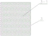
图中:1、转盘,2、硅片,3、工作台,3-1、吸气孔,4、限位框,5、弯管接头,6、支撑块,7、印刷头,8、支架,9、毛刷,10、风刀,11、上料工位、12、印刷工位,13、下料工位,14、清洁工位。In the figure: 1. Turntable, 2. Silicon wafer, 3. Workbench, 3-1. Suction hole, 4. Limit frame, 5. Elbow joint, 6. Support block, 7. Printing head, 8. Bracket , 9, hair brush, 10, air knife, 11, feeding station, 12, printing station, 13, unloading station, 14, cleaning station.
具体实施方式Detailed ways
现在结合附图对本发明作详细的说明。此图为简化的示意图,仅以示意方式说明本发明的基本结构,因此其仅显示与本发明有关的构成。The present invention will be described in detail in conjunction with accompanying drawing now. This figure is a simplified schematic diagram only illustrating the basic structure of the present invention in a schematic manner, so it only shows the components relevant to the present invention.
如图1-6所示,本发明的一种硅片清洁装置,包括转盘1、传送机构、限位机构、顶板机构以及清洁机构,所述转盘1上沿周向设有上料工位11、印刷工位12、下料工位13和清洁工位14,且每个工位上设有一个工作台3,四个所述工作台3沿所述转盘1周向均匀分布,所述工作台3边长与所述硅片2边长相同,所述工作台3上设有多个吸气孔3-1;As shown in Figures 1-6, a silicon wafer cleaning device of the present invention includes a
所述限位机构包括矩形限位框4,所述限位框4设于所述上料工位11工作台3上方,所述限位框4下端面由内框向外框方向逐渐向下倾斜,所述限位框4内框边长小于所述工作台3边长,所述限位框4外框边长大于所述工作台3边长,所述限位框4与所述上料工位11工作台3同轴,所述限位框4上端设有用于控制所述限位框4靠近或远离所述上料工位11工作台3的第一驱动装置;Described limit mechanism comprises
所述顶板机构包括依次连接的弯管接头5和支撑块6,所述弯管接头5为具有四分之一圆的弧形管状结构,所述工作台3底部均设有所述弯管接头5,所述弯管接头5一端与所述工作台3底端固定连接,所述弯管接头5另一端与所述支撑块6固定连接,所述支撑块6为外径与所述弯管接头5外径相同的四分之一圆形结构,所述支撑块6圆心与所述转盘1底端铰接,所述支撑块6上设有用于驱动所述支撑块6围绕圆心转动的第二驱动装置,所述第二驱动装置为气缸,所述气缸输出端与所述支撑块6远离所述弯管接头5的一侧铰接;The top plate mechanism includes an
所述清洁机构包括风刀10、毛刷9以及用于固定风刀10和毛刷9的支架8,所述支架8竖直设于所述上料工位11的工作台3上方且位于靠近所述转盘1轴心的一侧,所述支架8上设有驱动所述支架8沿竖直方向上下移动的第三驱动装置。Described cleaning mechanism comprises
所述传送机构包括用于将硅片2移至所述上料工位11的工作台3上的吸盘。The transfer mechanism includes a suction cup for moving the
工作原理:working principle:
通过吸盘将输送带上的硅片2吸至上料工位11工作台3上,第一驱动装置驱动限位框4沿竖直方向上升将硅片2位置矫正,吸气孔3-1吸气将硅片2固定在工作台3上,第二驱动装置驱动支撑块6将弯管接头5顶出转盘1上表面,使工作台3和硅片2竖直设置,第三驱动机构驱动支架8带动毛刷9和风刀10对硅片2表面进行清洁,清洁结束后,第二驱动装置驱动驱动块将弯管接头5下拉,使工作台3和硅片2水平设于转盘1上,转盘1转动使工作台3移至印刷工位12,印刷头7开始工作进行印刷。The
以上述依据本发明的理想实施例为启示,通过上述的说明内容,相关的工作人员完全可以在不偏离本发明的范围内,进行多样的变更以及修改。本项发明的技术范围并不局限于说明书上的内容,必须要根据权利要求范围来确定其技术性范围。Inspired by the ideal embodiment according to the present invention, through the above description, relevant workers can make various changes and modifications without departing from the scope of the present invention. The technical scope of the present invention is not limited to the content in the specification, and its technical scope must be determined according to the scope of the claims.
Claims (2)
Priority Applications (1)
| Application Number | Priority Date | Filing Date | Title |
|---|---|---|---|
| CN201710245583.8A CN106898570B (en) | 2017-04-14 | 2017-04-14 | Silicon wafer cleaning device |
Applications Claiming Priority (1)
| Application Number | Priority Date | Filing Date | Title |
|---|---|---|---|
| CN201710245583.8A CN106898570B (en) | 2017-04-14 | 2017-04-14 | Silicon wafer cleaning device |
Publications (2)
| Publication Number | Publication Date |
|---|---|
| CN106898570A CN106898570A (en) | 2017-06-27 |
| CN106898570B true CN106898570B (en) | 2023-06-20 |
Family
ID=59197517
Family Applications (1)
| Application Number | Title | Priority Date | Filing Date |
|---|---|---|---|
| CN201710245583.8A Active CN106898570B (en) | 2017-04-14 | 2017-04-14 | Silicon wafer cleaning device |
Country Status (1)
| Country | Link |
|---|---|
| CN (1) | CN106898570B (en) |
Families Citing this family (3)
| Publication number | Priority date | Publication date | Assignee | Title |
|---|---|---|---|---|
| CN109304951B (en) * | 2017-07-26 | 2021-06-25 | 天津环鑫科技发展有限公司 | Method for GPP screen printing passivation layer |
| CN107616158B (en) * | 2017-10-24 | 2020-07-03 | 深圳市康达深害虫防治有限公司 | Electric network device for mosquito trap |
| CN117772711A (en) * | 2022-09-22 | 2024-03-29 | 武汉锐晶激光芯片技术有限公司 | A kind of cleaning equipment and method |
Family Cites Families (8)
| Publication number | Priority date | Publication date | Assignee | Title |
|---|---|---|---|---|
| US5933902A (en) * | 1997-11-18 | 1999-08-10 | Frey; Bernhard M. | Wafer cleaning system |
| JP2002052370A (en) * | 2000-08-09 | 2002-02-19 | Ebara Corp | Substrate cleaning device |
| CN201913884U (en) * | 2010-11-19 | 2011-08-03 | 山东力诺太阳能电力股份有限公司 | Device for cleaning silicon wafer before printing |
| CN202293602U (en) * | 2011-10-31 | 2012-07-04 | 上海索日新能源科技有限公司 | Air blowing device for silk-screen printing feeding device |
| CN202540939U (en) * | 2012-04-19 | 2012-11-21 | 山东力诺太阳能电力股份有限公司 | Pre-screen-printing silicon chip cleaning device for solar batteries |
| CN204614764U (en) * | 2015-02-04 | 2015-09-02 | 晋能清洁能源科技有限公司 | Silicon Wafer Surface Microparticle Removal Device |
| CN104990383A (en) * | 2015-07-31 | 2015-10-21 | 北京七星华创电子股份有限公司 | On-line air knife drying device |
| CN206602102U (en) * | 2017-04-14 | 2017-10-31 | 常州亿晶光电科技有限公司 | Cleaning of silicon wafer device |
-
2017
- 2017-04-14 CN CN201710245583.8A patent/CN106898570B/en active Active
Also Published As
| Publication number | Publication date |
|---|---|
| CN106898570A (en) | 2017-06-27 |
Similar Documents
| Publication | Publication Date | Title |
|---|---|---|
| CN110379747B (en) | Full-automatic wafer cleaning and pasting integrated machine | |
| CN110379756B (en) | Full-automatic wafer lower wafer waxing return line and working method thereof | |
| CN106898570B (en) | Silicon wafer cleaning device | |
| JPH04363022A (en) | Cleaning device for wafer mounter | |
| CN110757313B (en) | A highly efficient automatic loading and unloading polishing machine | |
| CN110364464B (en) | Full-automatic multifunctional paster device and full-automatic paster process | |
| CN104241185A (en) | Substrate holding apparatus and substrate cleaning apparatus | |
| CN210040148U (en) | Full-automatic wafer cleaning and pasting all-in-one machine | |
| CN210359669U (en) | A robot-based automatic soldering equipment | |
| CN114193318A (en) | Sapphire substrate grinding automatic feeding and discharging production line and control method thereof | |
| CN106800185B (en) | A kind of curved surface screen printer of high automation | |
| CN111482863A (en) | Magnetic ring chamfering device and implementation method thereof | |
| CN109333844B (en) | A silicon wafer splitting device and silicon wafer dicing processing system | |
| CN110380685A (en) | A kind of two-sided test transmission device of IV, EL | |
| CN117428950A (en) | Wafer material cutting equipment and use method thereof | |
| CN209321935U (en) | A detection machine automatic loading and unloading device | |
| CN103606527B (en) | Semi-automatic wafer plants ball equipment | |
| CN114310545A (en) | Automatic chamfering equipment | |
| CN117705715B (en) | Wafer surface detection device and method based on machine vision | |
| CN207948017U (en) | Full-automatic SMD loaders | |
| CN206602102U (en) | Cleaning of silicon wafer device | |
| CN215373422U (en) | A silicon wafer drying device | |
| CN210876047U (en) | Automatic glue mixing and scraping system | |
| CN213494649U (en) | A rotary dispensing device for plastic workpieces | |
| CN110788976B (en) | A device for removing excess glaze in Jun porcelain production |
Legal Events
| Date | Code | Title | Description |
|---|---|---|---|
| PB01 | Publication | ||
| PB01 | Publication | ||
| SE01 | Entry into force of request for substantive examination | ||
| GR01 | Patent grant | ||
| GR01 | Patent grant |