CN1065373C - Convert circuit arrangement - Google Patents
Convert circuit arrangement Download PDFInfo
- Publication number
- CN1065373C CN1065373C CN96108641A CN96108641A CN1065373C CN 1065373 C CN1065373 C CN 1065373C CN 96108641 A CN96108641 A CN 96108641A CN 96108641 A CN96108641 A CN 96108641A CN 1065373 C CN1065373 C CN 1065373C
- Authority
- CN
- China
- Prior art keywords
- thyristor
- gto2
- gto1
- circuit arrangement
- inductance
- Prior art date
- Legal status (The legal status is an assumption and is not a legal conclusion. Google has not performed a legal analysis and makes no representation as to the accuracy of the status listed.)
- Expired - Fee Related
Links
Images


Classifications
-
- H—ELECTRICITY
- H02—GENERATION; CONVERSION OR DISTRIBUTION OF ELECTRIC POWER
- H02M—APPARATUS FOR CONVERSION BETWEEN AC AND AC, BETWEEN AC AND DC, OR BETWEEN DC AND DC, AND FOR USE WITH MAINS OR SIMILAR POWER SUPPLY SYSTEMS; CONVERSION OF DC OR AC INPUT POWER INTO SURGE OUTPUT POWER; CONTROL OR REGULATION THEREOF
- H02M7/00—Conversion of AC power input into DC power output; Conversion of DC power input into AC power output
- H02M7/42—Conversion of DC power input into AC power output without possibility of reversal
- H02M7/44—Conversion of DC power input into AC power output without possibility of reversal by static converters
- H02M7/48—Conversion of DC power input into AC power output without possibility of reversal by static converters using discharge tubes with control electrode or semiconductor devices with control electrode
- H02M7/505—Conversion of DC power input into AC power output without possibility of reversal by static converters using discharge tubes with control electrode or semiconductor devices with control electrode using devices of a thyratron or thyristor type requiring extinguishing means
- H02M7/515—Conversion of DC power input into AC power output without possibility of reversal by static converters using discharge tubes with control electrode or semiconductor devices with control electrode using devices of a thyratron or thyristor type requiring extinguishing means using semiconductor devices only
-
- H—ELECTRICITY
- H02—GENERATION; CONVERSION OR DISTRIBUTION OF ELECTRIC POWER
- H02M—APPARATUS FOR CONVERSION BETWEEN AC AND AC, BETWEEN AC AND DC, OR BETWEEN DC AND DC, AND FOR USE WITH MAINS OR SIMILAR POWER SUPPLY SYSTEMS; CONVERSION OF DC OR AC INPUT POWER INTO SURGE OUTPUT POWER; CONTROL OR REGULATION THEREOF
- H02M1/00—Details of apparatus for conversion
- H02M1/32—Means for protecting converters other than automatic disconnection
- H02M1/34—Snubber circuits
-
- H—ELECTRICITY
- H02—GENERATION; CONVERSION OR DISTRIBUTION OF ELECTRIC POWER
- H02M—APPARATUS FOR CONVERSION BETWEEN AC AND AC, BETWEEN AC AND DC, OR BETWEEN DC AND DC, AND FOR USE WITH MAINS OR SIMILAR POWER SUPPLY SYSTEMS; CONVERSION OF DC OR AC INPUT POWER INTO SURGE OUTPUT POWER; CONTROL OR REGULATION THEREOF
- H02M7/00—Conversion of AC power input into DC power output; Conversion of DC power input into AC power output
- H02M7/42—Conversion of DC power input into AC power output without possibility of reversal
- H02M7/44—Conversion of DC power input into AC power output without possibility of reversal by static converters
- H02M7/48—Conversion of DC power input into AC power output without possibility of reversal by static converters using discharge tubes with control electrode or semiconductor devices with control electrode
- H02M7/505—Conversion of DC power input into AC power output without possibility of reversal by static converters using discharge tubes with control electrode or semiconductor devices with control electrode using devices of a thyratron or thyristor type requiring extinguishing means
- H02M7/515—Conversion of DC power input into AC power output without possibility of reversal by static converters using discharge tubes with control electrode or semiconductor devices with control electrode using devices of a thyratron or thyristor type requiring extinguishing means using semiconductor devices only
- H02M7/519—Conversion of DC power input into AC power output without possibility of reversal by static converters using discharge tubes with control electrode or semiconductor devices with control electrode using devices of a thyratron or thyristor type requiring extinguishing means using semiconductor devices only in a push-pull configuration
-
- H—ELECTRICITY
- H02—GENERATION; CONVERSION OR DISTRIBUTION OF ELECTRIC POWER
- H02M—APPARATUS FOR CONVERSION BETWEEN AC AND AC, BETWEEN AC AND DC, OR BETWEEN DC AND DC, AND FOR USE WITH MAINS OR SIMILAR POWER SUPPLY SYSTEMS; CONVERSION OF DC OR AC INPUT POWER INTO SURGE OUTPUT POWER; CONTROL OR REGULATION THEREOF
- H02M1/00—Details of apparatus for conversion
- H02M1/32—Means for protecting converters other than automatic disconnection
- H02M1/34—Snubber circuits
- H02M1/346—Passive non-dissipative snubbers
-
- Y—GENERAL TAGGING OF NEW TECHNOLOGICAL DEVELOPMENTS; GENERAL TAGGING OF CROSS-SECTIONAL TECHNOLOGIES SPANNING OVER SEVERAL SECTIONS OF THE IPC; TECHNICAL SUBJECTS COVERED BY FORMER USPC CROSS-REFERENCE ART COLLECTIONS [XRACs] AND DIGESTS
- Y02—TECHNOLOGIES OR APPLICATIONS FOR MITIGATION OR ADAPTATION AGAINST CLIMATE CHANGE
- Y02B—CLIMATE CHANGE MITIGATION TECHNOLOGIES RELATED TO BUILDINGS, e.g. HOUSING, HOUSE APPLIANCES OR RELATED END-USER APPLICATIONS
- Y02B70/00—Technologies for an efficient end-user side electric power management and consumption
- Y02B70/10—Technologies improving the efficiency by using switched-mode power supplies [SMPS], i.e. efficient power electronics conversion e.g. power factor correction or reduction of losses in power supplies or efficient standby modes
Landscapes
- Engineering & Computer Science (AREA)
- Power Engineering (AREA)
- Power Conversion In General (AREA)
- Semiconductor Integrated Circuits (AREA)
- Rectifiers (AREA)
- Inverter Devices (AREA)
- Thyristor Switches And Gates (AREA)
- Ac-Ac Conversion (AREA)
Abstract
本发明提出了一种换流器电路装置,其中,可关断晶闸管受到控制。晶闸管电路的特征在于,只具有少量元器件。
The invention proposes a converter circuit arrangement in which thyristors which can be switched off are controlled. Thyristor circuits are characterized by having only a small number of components.
Description
本发明涉及大功率电子领域。The invention relates to the field of high-power electronics.
譬如在W.MC Murray在电气与电子工程师协会大功率电子会刊,第二卷、第三期(1987年7月)发表的题为“用于电压源可关断晶闸管(GTO)换流器的有效缓冲器”的论文中描述了这种电路装置。所描述的是具有至少两个串联的可关断晶闸管(GTO)的换流器电路装置,其中,这些可关断晶闸管(GTO)与一个直流电源相接并以串联的一个公共节点形成一个负载接口。此外,设有与这些可关断晶闸管(GTO)并联的所谓反并联二极管,这些反并联二极管在换向后接收导通电流。为了在转换时面对过陡的电流和电压斜率保护可关断晶闸管(GTO),必须设置一个电路或英文中所称“缓冲器”。按照现有技术,该电路如在提及的论文中所描述的那样,包括一个比较昂贵的、由电感、电容器、电阻和二极管构成的线路。A.Ferraro在电气与电子工程师协会会刊1982年,第466至467页上刊登的题为“用于晶体管换流器的低损耗缓冲器技术综述”的论文公开了其它的电路派生形式。For example in W. MC Murray, "Efficient snubbers for voltage source turn-off thyristor (GTO) converters, IEEE Transactions on High Power Electronics, Vol. 2, No. 3 (July 1987). "The paper described this circuit device. Described is a converter circuit arrangement having at least two series-connected turn-off thyristors (GTOs), wherein the turn-off thyristors (GTOs) are connected to a DC power supply and form a load with a common node connected in series interface. Furthermore, parallel to these turn-off thyristors (GTOs), so-called anti-parallel diodes are provided, which receive the conduction current after commutation. To protect turn-off thyristors (GTOs) against excessively steep current and voltage slopes during transitions, a circuit or what is called a "snubber" in English must be provided. According to the prior art, this circuit, as described in the cited article, comprises a relatively expensive circuit consisting of inductors, capacitors, resistors and diodes. A. Other circuit derivatives are disclosed in Ferraro's paper entitled "A Review of Low-Loss Snubber Techniques for Transistor Converters" Proceedings of the Institute of Electrical and Electronics Engineers, 1982, pp. 466-467.
在同一发明人的欧洲专利申请EP-A1-0489945和WO-93/09600中描述了对可关断晶闸管(GTO)的所谓“控制”并提供了用于相应控制单元的电路装置。涉及上述两个欧洲专利申请,人们把“控制”这一概念理解为用一个控制极电流控制可关断晶闸管(GTO),该控制极电流的形状在于,断路放大率IA/IG峰值明显的小于3并且产生一个至少为1kv/μs的阳极电压上升速度。该控制在本发明的范畴内具有意义,并因此应把上述欧洲专利申请的内容明确地纳入此处。In the European patent applications EP-A1-0489945 and WO-93/09600 of the same inventor a so-called "control" of a turn-off thyristor (GTO) is described and a circuit arrangement for a corresponding control unit is provided. Referring to the above two European patent applications, the concept of "control" is understood as controlling the turn-off thyristor (GTO) with a gate current whose shape is such that the peak value of the open circuit amplification ratio IA/IG is significantly smaller than 3 and produce an anode voltage rise rate of at least 1kv/μs. This control is meaningful within the scope of the present invention, and the content of the above-mentioned European patent application should therefore be expressly incorporated here.
本发明的目的在于提供一种具有可关断晶闸管(GTO)的换流器电路装置,该电路装置只需由极少的电路元器件构成并因此只要求极少的占用面积并可费用合理地完成制作。The object of the present invention is to provide a converter circuit arrangement with turn-off thyristors (GTOs), which circuit arrangement only needs to be composed of very few circuit components and therefore requires only a very small footprint and can be cost-effective Finished making.
在本发明书开头所述类型的电路装置中,解决以上任务的技术方案在于以下特征:In a circuit arrangement of the type mentioned at the beginning of the present invention, the technical solution to the above task is characterized by the following:
具有至少一个分路的换流器电路装置,该分路具有偶数个串联的可关断晶闸管并具有与晶闸管反并联的反并联二极管,所述分路或每个分路与一直流电源相连接并且该分路或每个分路的一个中间节点形成一个负载端,并且还具有限制电流和电压上升速度的装置,这些装置可防止过高的电流和电压上升速度从而保护可关断晶闸管,其中可关断晶闸管受到控制,并且在每个分路中,限制电压上升速度的装置最少只包括一个电容器,该电容器是与相应的晶闸管的反并联二极管之一并联设置的。Inverter circuit arrangement having at least one branch with an even number of switchable thyristors connected in series and with antiparallel diodes antiparallel to the thyristors, the or each branch being connected to a DC power supply and an intermediate node of the or each branch forms a load terminal and also has means for limiting current and voltage rise rates which prevent excessive current and voltage rise rates thereby protecting the turn-off thyristors, wherein The turn-off thyristors are controlled and the means for limiting the rate of voltage rise in each branch comprises at least one capacitor arranged in parallel with one of the anti-parallel diodes of the corresponding thyristor.
发明的核心是:可关断晶闸管(GTO)受到控制,并且限制电压上升速度的装置只包括一个电容器,该电容器与反并联二极管之一并联。其中,电容器与哪个反并联二极管并联或者是否为每个反并联二极管设置一个电容器是不重要的。The heart of the invention is that the turn-off thyristor (GTO) is controlled and the means for limiting the speed of voltage rise consists of only a capacitor connected in parallel with one of the anti-parallel diodes. In this case, it is immaterial to which anti-parallel diode the capacitor is connected in parallel or whether a capacitor is provided for each anti-parallel diode.
这种控制方式连同发明的限制电压上升速度的装置可使譬如用于公开的Mc Marry电路和undeland电路的限制电流上升速度的装置得以简化。特别是可取消所有的电阻和二极管。并且大大缩小了留下的电容器和电感的参数值。This type of control, together with the inventive means for limiting the rate of voltage rise, allows for the simplification of the means for limiting the rate of current rise, such as those used in the disclosed McMarry and undeland circuits. In particular, all resistors and diodes can be omitted. And the parameter values of the remaining capacitors and inductors are greatly reduced.
下面借助实施例结合附图详细说明本发明。附图所示为:The present invention will be described in detail below by means of embodiments in conjunction with the accompanying drawings. The accompanying drawings show:
图1为发明的第一实施例的电路图;Fig. 1 is the circuit diagram of the first embodiment of the invention;
图2为发明的第二实施例的电路图;Fig. 2 is the circuit diagram of the second embodiment of the invention;
图3为发明的另一实施例的电路图;Fig. 3 is the circuit diagram of another embodiment of the invention;
图4为发明的一个只由电极少电路元器件构成的实施例的电路图。Fig. 4 is a circuit diagram of an embodiment of the invention consisting of only a few circuit components.
图中所用的标号及其意义汇总列于标号一览表中,图中的相同的构件原则上用相同的标号表示。The symbols used in the figure and their meanings are summarized in the list of symbols, and the same components in the figure are denoted by the same symbols in principle.
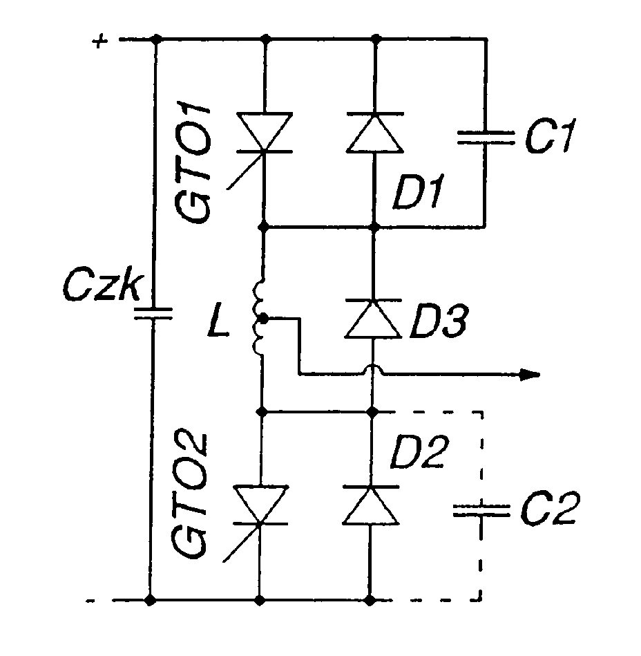
图1示出了发明的第一个实施例的等效电路图。按照发明,电路装置的可关断晶闸管(GTO)受到控制。做为新的负荷极限,出现动态的、在断路过程中出现的雪崩效应。半导体芯片提供的硅接触面可得到均匀的利用。通过控制可加速接通过程,使可关断晶闸管的破坏极限可由目前的500A/μs提高到3000A/μs以上。在图1中示出了一个具有一个第一可关断晶闸管GTO1和一个第二可关断晶闸管GTO2以及与此反并联的二极管D1和D2的分路。该分路与一个通过中间电路电容器Czk表示的直流电源的正极和负极相接。按照公知的方式(见曾被提及的现有技术文件),可关断晶闸管(GTO)交替地被一个图中未示出的控制单元控制,使负载接口上产生一个交流电压。当然可设置多个相同结构的、可用以建立一个多相的交流电压系统的分路。但为清晰起见,在图中只示出了一个分路。Fig. 1 shows an equivalent circuit diagram of the first embodiment of the invention. According to the invention, turn-off thyristors (GTOs) of the circuit arrangement are controlled. As a new load limit, a dynamic avalanche effect occurs during the disconnection process. The silicon contact area provided by the semiconductor chip can be used evenly. The turn-on process can be accelerated through control, so that the damage limit of the turn-off thyristor can be increased from the current 500A/μs to more than 3000A/μs. FIG. 1 shows a shunt with a first turn-off thyristor GTO1 and a second turn-off thyristor GTO2 as well as diodes D1 and D2 connected in antiparallel thereto. This branch is connected to the positive and negative poles of a DC power supply represented by an intermediate circuit capacitor Czk. In a known manner (see the prior art document mentioned above), the turn-off thyristors (GTOs) are alternately controlled by a control unit (not shown) so that an alternating voltage is generated at the load connection. It is of course possible to provide a plurality of identically constructed sub-circuits which can be used to create a polyphase alternating voltage system. However, for the sake of clarity, only one branch is shown in the figure.
按照图1所示的实施例,限制电压上升速度的装置为每个分路只包括一个电容器C1或C2,该电容器与一个与相应的可关断晶闸管(GTO)反并联设置的反并联二极管D1或D2并联。电容器C1或C2或者配属于一个晶闸管(GTO1),或者配属于另一个晶闸管(GTO2)。但也可为每个晶闸管设置一个与每个反并联二极管并联的电容器。According to the embodiment shown in FIG. 1, the means for limiting the rate of rise of the voltage comprise for each branch only one capacitor C1 or C2, which is connected with an antiparallel diode D1 arranged in antiparallel with the corresponding turn-off thyristor (GTO). Or D2 in parallel. Capacitor C1 or C2 is assigned either to one thyristor (GTO1) or to the other thyristor (GTO2). However, a capacitor connected in parallel with each anti-parallel diode can also be provided for each thyristor.
与公开的Mc Marry电路相比,取消了处于反并联二极管和电容器之间的、所谓的缓冲二极管和无载运行电阻。据此,限制电流上升速度的装置现在只包括一个处于一个分路的两个可关断晶闸管(GTO)之间的电感L和一个与该电感L并联的二极管D3。分路的负载接口或者可通过电感L的线圈的中间抽头形成,或者可通过两个独立的、串联的线圈的公共节点形成。Compared to the disclosed McMarry circuit, the so-called snubber diode and no-load running resistor between the antiparallel diode and capacitor are eliminated. Accordingly, the means for limiting the rate of rise of the current now consist only of an inductance L between two turn-off thyristors (GTOs) of a shunt and a diode D3 connected in parallel with this inductance L. The shunted load connection can be formed either by a center tap of the coil of the inductance L or by a common node of two separate, series-connected coils.
发明的范畴包括:或者每个分路只设一个电容器,或者为每个晶闸管分别设置一个电容器。在只设一个电容器的情况下,该电容器的电容量等于各个电容器电容量的总和。The scope of the invention includes either only one capacitor per branch or one capacitor per thyristor. In the case of only one capacitor, the capacitance of the capacitor is equal to the sum of the capacitances of the individual capacitors.
通过本发明,机械结构也被简化,因为每个电路由需要10个散热体减为只需要7至8个散热体。留下的电路元器件的参数值也可缩小。在中间回路电压为3kv时,在电容器C1和C2只存在一个电容器的情况下,所需的电容量值由3μF缩小到只为0.5或1μF,所需的电感值由10μH减至2μH。规格设计的准则可在于,作为电路装置设计依据的最大断路电流与一个或多个电容器电容量的总和之比应大于或等于2kv/μs。计算一个或多个电感量的准则在于,中间回路电压与电感量的总和之比应大于或等于1KA/μs。Through the present invention, the mechanical structure is also simplified, because each circuit requires only 7 to 8 heat sinks instead of 10 heat sinks. The parameter values of the remaining circuit components can also be scaled down. When the intermediate circuit voltage is 3kv, when there is only one capacitor in capacitors C1 and C2, the required capacitance value is reduced from 3μF to only 0.5 or 1μF, and the required inductance value is reduced from 10μH to 2μH. The criterion for specification design may be that the ratio of the maximum breaking current used as the basis for the design of the circuit arrangement to the sum of the capacitances of one or more capacitors should be greater than or equal to 2kv/μs. The criterion for calculating one or more inductances is that the ratio of the intermediate circuit voltage to the sum of the inductances should be greater than or equal to 1KA/μs.
在图2中示出了图1所示电路的一个派生形式。其中,限制电流上升速度的装置的电感L1或L2设在反并联二极管D1、D2和相应的可关断晶闸管GTO1、GTO2之间。二极管D3设在两个可关断晶闸管之间,并且通过两个反并联二极管D1和D2的连接形成负载接口。在该电路装置中,可应用GTO其阳极-阴极间电压在反向负荷时被限制到约20至100V。据此,通过向馈电电路中分流,使正在关断的可关断晶闸管GTO上的过电压受到限制。因此,这种类型的电路可应用具有阳极短路器的常规可关断晶闸管(GTO)。A derivative of the circuit shown in FIG. 1 is shown in FIG. 2 . Wherein, the inductance L1 or L2 of the device for limiting the current rising speed is arranged between the anti-parallel diodes D1, D2 and the corresponding turn-off thyristors GTO1, GTO2. Diode D3 is arranged between the two turn-off thyristors and forms the load interface via the connection of two anti-parallel diodes D1 and D2. In this circuit arrangement, a GTO can be used whose anode-cathode voltage is limited to approximately 20 to 100 V under reverse load. Accordingly, the overvoltage on the turn-off thyristor GTO being turned off is limited by shunting the current into the feed circuit. Therefore, a conventional turn-off thyristor (GTO) with an anode shunt can be used for this type of circuit.
在图3中示出了发明的一个从所谓的undeland电路派生出的实施形式。又是分别有一个反并联二极管D1和D2与一个分路的可关断晶闸管GTO1和GTO2并联。限制电压上升速度的装置每个分路包括至少一个电容器C1或C2,该电容器与相应的反并联二极管直接并联。在该实施形式中,也可有选择地仅设一个电容器,或为每个晶闸管设置一个电容器。与图1和2所示的实施形式不同之处在于,限制电流上升速度的装置不是设在两个可关断晶闸管(GTO)之间,而是面对直流电源的正极或负极。在图3所示的实施形式中,该限制电流上升速度的装置面对正极并包括一个电感L和一个与该电感并联的二极管D3。An embodiment of the invention derived from the so-called undeland circuit is shown in FIG. 3 . Again, an anti-parallel diode D1 and D2 are respectively connected in parallel with a shunted turn-off thyristor GTO1 and GTO2. The means for limiting the rate of rise of the voltage comprises, per branch, at least one capacitor C1 or C2 connected directly in parallel with the corresponding anti-parallel diode. Alternatively, only one capacitor, or one capacitor per thyristor, can also be provided in this embodiment. The difference from the embodiment shown in Figures 1 and 2 is that the means for limiting the rate of current rise is not located between two turn-off thyristors (GTOs), but faces the positive or negative pole of the DC power supply. In the embodiment shown in FIG. 3 , the means for limiting the rate of rise of the current faces the positive pole and comprises an inductor L and a diode D3 connected in parallel with the inductor.
图4示出了一个由最少的电路元器件构成的实施形式:可应用具有反向雪崩特性(譬如基于阳极短路器或一个集成在内的雪崩区)的可关断晶闸管(GTO)建立电路,其中,在每个分路中不仅可关断晶闸管GTO1和GTO2,而且所属的反并联二极管D1和D2均在直流电源的正极和负极之间串联。对电流上升速度的限制是通过一个在分路中处于可关断晶闸管(GTO)和二极管之间的电感L完成的。限制电压上升速度的装置包括至少一个电容器C2,该电容器可有选择地与反并联二极管D1或D2之一并联。具有一个附加的、与可关断晶闸管(GTO)之一并联的电容器C3的电路装置是特别相宜的。在该电路装置中也可只设一个电容器,或者分别设置与每个反并联二极管并联的电容器。Figure 4 shows an implementation with a minimum of circuit components: a turn-off thyristor (GTO) with a reverse avalanche characteristic (e.g. based on an anode short-circuit or an integrated avalanche zone) can be used to build the circuit, In each branch, not only the thyristors GTO1 and GTO2 can be turned off, but also the associated anti-parallel diodes D1 and D2 are connected in series between the positive pole and the negative pole of the DC power supply. Limiting the rate of current rise is accomplished by an inductor L in the shunt between the turn-off thyristor (GTO) and the diode. The means for limiting the rate of rise of the voltage comprises at least one capacitor C2 selectively connected in parallel with one of the anti-parallel diodes D1 or D2. A circuit arrangement with an additional capacitor C3 connected in parallel to one of the turn-off thyristors (GTO) is particularly expedient. It is also possible to provide only one capacitor in the circuit arrangement, or to provide separate capacitors connected in parallel to each anti-parallel diode.
在所有的、上述的电路装置中,一个反并联二极管可被两个具有一半效能的串联二极管取代。在中间回路电压为3KV的情况下,每个可关断晶闸管或者需一个4.5KV的反并联二极管,或者需两个2.5KV的二极管。二极管D3最好具有高的正向电压。据此,可压缩空转时间并减少反向恢复的影响。因此,整个电路装置更能抗衡因反向恢复引起的故障,譬如通过比对传统二极管更大剂量的电子幅照可得到这样的二极管。In all of the circuit arrangements described above, one antiparallel diode can be replaced by two series diodes with half the efficiency. In the case of an intermediate circuit voltage of 3KV, each turn-off thyristor requires either a 4.5KV anti-parallel diode or two 2.5KV diodes. Diode D3 preferably has a high forward voltage. Accordingly, the idle time can be compressed and the effect of reverse recovery can be reduced. Thus, the entire circuit arrangement is more resistant to failures due to reverse recovery, for example such diodes being obtainable by irradiation with a higher dose of electrons than conventional diodes.
总之,本发明提供了用少量的电路元器件构成电路装置的必要条件。其中,分路的数量可任意选择。为了提高耐压强度。也可串联可关断晶闸管。In summary, the invention provides the requisites for constructing a circuit arrangement with a small number of circuit components. Wherein, the number of branches can be selected arbitrarily. In order to improve the compressive strength. Turn-off thyristors can also be connected in series.
Claims (9)
Applications Claiming Priority (2)
| Application Number | Priority Date | Filing Date | Title |
|---|---|---|---|
| DE19523095.7 | 1995-06-26 | ||
| DE19523095A DE19523095A1 (en) | 1995-06-26 | 1995-06-26 | Power converter circuitry |
Publications (2)
| Publication Number | Publication Date |
|---|---|
| CN1145547A CN1145547A (en) | 1997-03-19 |
| CN1065373C true CN1065373C (en) | 2001-05-02 |
Family
ID=7765232
Family Applications (1)
| Application Number | Title | Priority Date | Filing Date |
|---|---|---|---|
| CN96108641A Expired - Fee Related CN1065373C (en) | 1995-06-26 | 1996-06-26 | Convert circuit arrangement |
Country Status (11)
| Country | Link |
|---|---|
| US (1) | US5731967A (en) |
| EP (1) | EP0751612A3 (en) |
| JP (1) | JPH0919165A (en) |
| KR (1) | KR970004259A (en) |
| CN (1) | CN1065373C (en) |
| CA (1) | CA2174818A1 (en) |
| CZ (1) | CZ290776B6 (en) |
| DE (1) | DE19523095A1 (en) |
| IN (1) | IN193010B (en) |
| SK (1) | SK79696A3 (en) |
| TW (1) | TW307940B (en) |
Families Citing this family (11)
| Publication number | Priority date | Publication date | Assignee | Title |
|---|---|---|---|---|
| JPH10164843A (en) * | 1996-12-02 | 1998-06-19 | Toshiba Corp | Power converter |
| KR100433954B1 (en) * | 1999-08-04 | 2004-06-04 | 주식회사 포스코 | Snubber circuit for three level gate turn-off thyristor inverter/converter |
| EP1195886A1 (en) * | 2000-09-29 | 2002-04-10 | ABB Schweiz AG | Backward conducting gate commutated thyristor and application thereof |
| RU2396665C2 (en) * | 2006-01-20 | 2010-08-10 | Абб Текнолоджи Лтд. | Converter |
| JP2009004499A (en) * | 2007-06-20 | 2009-01-08 | Kansai Electric Power Co Inc:The | Pn diode, electric circuit device, and power conversion device |
| JP5304416B2 (en) * | 2009-04-28 | 2013-10-02 | 富士電機株式会社 | Power conversion circuit |
| US20120049834A1 (en) * | 2009-05-07 | 2012-03-01 | The Curators Of The University Of Missouri | Circuit and method to suppress the parasitic resonance from a dc/dc converter |
| CN103019143B (en) * | 2011-09-26 | 2016-04-20 | 西门子瑞士有限公司 | Notification appliance circuit and notice system |
| CN102830740B (en) * | 2012-08-23 | 2014-04-30 | 矽力杰半导体技术(杭州)有限公司 | High-efficiency bias voltage generating circuit |
| DE202013104510U1 (en) * | 2013-10-04 | 2013-11-14 | Abb Technology Ag | Semiconductor stack for converters with snubber capacitors |
| EP4119957A1 (en) * | 2021-07-16 | 2023-01-18 | Siemens Energy Global GmbH & Co. KG | Method for monitoring a protective device |
Citations (2)
| Publication number | Priority date | Publication date | Assignee | Title |
|---|---|---|---|---|
| DE2931070A1 (en) * | 1979-07-28 | 1981-02-12 | Licentia Gmbh | Inverter with forced commutation employing gate-turn-off thyristors - has capacitor across each thyristor to suppress dangerous switch off transients |
| US5237225A (en) * | 1990-12-08 | 1993-08-17 | Asea Brown Boveri Ltd. | Switching arrangement for an rf gto |
Family Cites Families (10)
| Publication number | Priority date | Publication date | Assignee | Title |
|---|---|---|---|---|
| DE3215589A1 (en) * | 1982-04-27 | 1983-10-27 | Rainer Dipl Ing Marquardt | Suppressor circuit without fundamental losses for electronic pairs of arms connected in antiparallel |
| DE3544232A1 (en) * | 1985-12-12 | 1987-06-19 | Licentia Gmbh | Circuit arrangement for overcurrent limiting in an invertor having power semiconductors, for example GTO thyristors, which can be turned off |
| DE3743436C1 (en) * | 1987-12-21 | 1989-05-11 | Siemens Ag | Switch-relieved, low-loss three-point inverter |
| DE3801327A1 (en) * | 1988-01-19 | 1989-07-27 | Asea Brown Boveri | RELIEF NETWORK FOR INTERLOCK-FREE BRANCHES OF A MULTI-PHASE RECTIFIER |
| DE3823399A1 (en) * | 1988-01-28 | 1989-08-10 | Asea Brown Boveri | Relief network for electronic branch pairs in a reverse-parallel circuit |
| DE3822493A1 (en) * | 1988-07-02 | 1990-01-04 | Asea Brown Boveri | RETURNING RELIEF NETWORK FOR ELECTRONIC BRANCHES IN ANTIPARALLEL CIRCUIT |
| DD278452A1 (en) * | 1988-12-21 | 1990-05-02 | Elektroprojekt Anlagenbau Veb | ARRANGEMENT NETWORK FOR SEMICONDUCTOR SWITCHES IN MULTI-PHASE ARRANGEMENT |
| DE4121177A1 (en) * | 1990-06-23 | 1992-01-16 | Licentia Gmbh | Switch=off circuitry for discharge of inverter branch pairs - consists of two gate-controlled semiconductor switches arranged between poles of DC voltage source |
| DE4136181A1 (en) * | 1991-11-02 | 1993-05-06 | Asea Brown Boveri Ag, Baden, Aargau, Ch | GTO THYRISTOR CIRCUIT |
| US5448467A (en) * | 1992-04-13 | 1995-09-05 | Ferreira; Jan A. | Electrical power converter circuit |
-
1995
- 1995-06-26 DE DE19523095A patent/DE19523095A1/en not_active Withdrawn
-
1996
- 1996-04-18 IN IN649MA1996 patent/IN193010B/en unknown
- 1996-04-20 TW TW085104736A patent/TW307940B/zh active
- 1996-04-23 CA CA002174818A patent/CA2174818A1/en not_active Abandoned
- 1996-05-31 EP EP96810351A patent/EP0751612A3/en not_active Withdrawn
- 1996-06-03 KR KR1019960019648A patent/KR970004259A/en not_active Ceased
- 1996-06-11 JP JP8149466A patent/JPH0919165A/en active Pending
- 1996-06-11 CZ CZ19961705A patent/CZ290776B6/en not_active IP Right Cessation
- 1996-06-18 SK SK796-96A patent/SK79696A3/en unknown
- 1996-06-26 US US08/670,646 patent/US5731967A/en not_active Expired - Fee Related
- 1996-06-26 CN CN96108641A patent/CN1065373C/en not_active Expired - Fee Related
Patent Citations (2)
| Publication number | Priority date | Publication date | Assignee | Title |
|---|---|---|---|---|
| DE2931070A1 (en) * | 1979-07-28 | 1981-02-12 | Licentia Gmbh | Inverter with forced commutation employing gate-turn-off thyristors - has capacitor across each thyristor to suppress dangerous switch off transients |
| US5237225A (en) * | 1990-12-08 | 1993-08-17 | Asea Brown Boveri Ltd. | Switching arrangement for an rf gto |
Also Published As
| Publication number | Publication date |
|---|---|
| CA2174818A1 (en) | 1996-12-27 |
| EP0751612A3 (en) | 1998-04-22 |
| TW307940B (en) | 1997-06-11 |
| SK79696A3 (en) | 1998-02-04 |
| IN193010B (en) | 2004-06-19 |
| DE19523095A1 (en) | 1997-01-02 |
| EP0751612A2 (en) | 1997-01-02 |
| US5731967A (en) | 1998-03-24 |
| CZ290776B6 (en) | 2002-10-16 |
| JPH0919165A (en) | 1997-01-17 |
| KR970004259A (en) | 1997-01-29 |
| CZ170596A3 (en) | 1997-01-15 |
| CN1145547A (en) | 1997-03-19 |
Similar Documents
| Publication | Publication Date | Title |
|---|---|---|
| CN1108657C (en) | Power inverter device | |
| CN1291543C (en) | Fault-tolerant power conversion circuit | |
| US10044258B2 (en) | Active snubber | |
| EP3174190A1 (en) | Three level converter | |
| US5982646A (en) | Voltage clamp snubbers for three level converter | |
| EP0834212B1 (en) | Converter circuit, circuitry having at least one switching device and circuit module | |
| JP4502510B2 (en) | VSC converter | |
| CN101253677A (en) | Pulse resistor (breaking resistor) for frequency converters in the high-voltage and high-power range | |
| CN101238635A (en) | Multilevel AC/DC Converters for Traction Applications | |
| CN108702105A (en) | For modularization multi-level converter Shuangzi module and include the modularization multi-level converter of the Shuangzi module | |
| CN1157503A (en) | Rectifier circuit arrangement | |
| JP6597917B2 (en) | 3-level inverter | |
| CN1065373C (en) | Convert circuit arrangement | |
| CN108702084A (en) | Converter | |
| CN1270433C (en) | Method for protecting a matrix converter against overvoltages and an active overvoltage device | |
| JP3239757B2 (en) | AC current source circuit | |
| JPH09275674A (en) | Power converter | |
| CN108063562A (en) | Active three level neutral points clamper conversion module | |
| JPH07312878A (en) | Snubber circuit of 3-level inverter | |
| CN1113362A (en) | High-voltage self-excited conversion device for connection system | |
| JPH05161253A (en) | Snubber circuit for semiconductor power converter | |
| JP2004274801A (en) | Inverter circuit | |
| JPH0731158A (en) | Snubber energy recovery circuit for power converter | |
| JP2512242B2 (en) | Inverter device | |
| JP2555621B2 (en) | Inverter energy recovery circuit |
Legal Events
| Date | Code | Title | Description |
|---|---|---|---|
| C06 | Publication | ||
| PB01 | Publication | ||
| C10 | Entry into substantive examination | ||
| SE01 | Entry into force of request for substantive examination | ||
| C14 | Grant of patent or utility model | ||
| GR01 | Patent grant | ||
| C56 | Change in the name or address of the patentee |
Owner name: ABB SWITZERLAND HOLDINGS CO., LTD. Free format text: FORMER NAME OR ADDRESS: YA RUIYA BOLANGBOWLIC CO., LTD. |
|
| CP01 | Change in the name or title of a patent holder |
Patentee after: Asea Brown Boveri AB Patentee before: Asea Brown Boveri Ltd. |
|
| C19 | Lapse of patent right due to non-payment of the annual fee | ||
| CF01 | Termination of patent right due to non-payment of annual fee |