CN1065085C - Step-up switching power supply - Google Patents
Step-up switching power supply Download PDFInfo
- Publication number
- CN1065085C CN1065085C CN988002485A CN98800248A CN1065085C CN 1065085 C CN1065085 C CN 1065085C CN 988002485 A CN988002485 A CN 988002485A CN 98800248 A CN98800248 A CN 98800248A CN 1065085 C CN1065085 C CN 1065085C
- Authority
- CN
- China
- Prior art keywords
- mentioned
- capacitor
- magnetic element
- diode
- circuit
- Prior art date
- Legal status (The legal status is an assumption and is not a legal conclusion. Google has not performed a legal analysis and makes no representation as to the accuracy of the status listed.)
- Expired - Fee Related
Links
Images


Classifications
-
- H—ELECTRICITY
- H02—GENERATION; CONVERSION OR DISTRIBUTION OF ELECTRIC POWER
- H02M—APPARATUS FOR CONVERSION BETWEEN AC AND AC, BETWEEN AC AND DC, OR BETWEEN DC AND DC, AND FOR USE WITH MAINS OR SIMILAR POWER SUPPLY SYSTEMS; CONVERSION OF DC OR AC INPUT POWER INTO SURGE OUTPUT POWER; CONTROL OR REGULATION THEREOF
- H02M1/00—Details of apparatus for conversion
- H02M1/32—Means for protecting converters other than automatic disconnection
- H02M1/34—Snubber circuits
-
- H—ELECTRICITY
- H02—GENERATION; CONVERSION OR DISTRIBUTION OF ELECTRIC POWER
- H02M—APPARATUS FOR CONVERSION BETWEEN AC AND AC, BETWEEN AC AND DC, OR BETWEEN DC AND DC, AND FOR USE WITH MAINS OR SIMILAR POWER SUPPLY SYSTEMS; CONVERSION OF DC OR AC INPUT POWER INTO SURGE OUTPUT POWER; CONTROL OR REGULATION THEREOF
- H02M3/00—Conversion of dc power input into dc power output
- H02M3/02—Conversion of dc power input into dc power output without intermediate conversion into ac
- H02M3/04—Conversion of dc power input into dc power output without intermediate conversion into ac by static converters
- H02M3/10—Conversion of dc power input into dc power output without intermediate conversion into ac by static converters using discharge tubes with control electrode or semiconductor devices with control electrode
- H02M3/145—Conversion of dc power input into dc power output without intermediate conversion into ac by static converters using discharge tubes with control electrode or semiconductor devices with control electrode using devices of a triode or transistor type requiring continuous application of a control signal
- H02M3/155—Conversion of dc power input into dc power output without intermediate conversion into ac by static converters using discharge tubes with control electrode or semiconductor devices with control electrode using devices of a triode or transistor type requiring continuous application of a control signal using semiconductor devices only
-
- H—ELECTRICITY
- H03—ELECTRONIC CIRCUITRY
- H03K—PULSE TECHNIQUE
- H03K17/00—Electronic switching or gating, i.e. not by contact-making and –breaking
- H03K17/08—Modifications for protecting switching circuit against overcurrent or overvoltage
- H03K17/081—Modifications for protecting switching circuit against overcurrent or overvoltage without feedback from the output circuit to the control circuit
- H03K17/0814—Modifications for protecting switching circuit against overcurrent or overvoltage without feedback from the output circuit to the control circuit by measures taken in the output circuit
-
- H—ELECTRICITY
- H02—GENERATION; CONVERSION OR DISTRIBUTION OF ELECTRIC POWER
- H02M—APPARATUS FOR CONVERSION BETWEEN AC AND AC, BETWEEN AC AND DC, OR BETWEEN DC AND DC, AND FOR USE WITH MAINS OR SIMILAR POWER SUPPLY SYSTEMS; CONVERSION OF DC OR AC INPUT POWER INTO SURGE OUTPUT POWER; CONTROL OR REGULATION THEREOF
- H02M1/00—Details of apparatus for conversion
- H02M1/32—Means for protecting converters other than automatic disconnection
- H02M1/34—Snubber circuits
- H02M1/346—Passive non-dissipative snubbers
-
- Y—GENERAL TAGGING OF NEW TECHNOLOGICAL DEVELOPMENTS; GENERAL TAGGING OF CROSS-SECTIONAL TECHNOLOGIES SPANNING OVER SEVERAL SECTIONS OF THE IPC; TECHNICAL SUBJECTS COVERED BY FORMER USPC CROSS-REFERENCE ART COLLECTIONS [XRACs] AND DIGESTS
- Y02—TECHNOLOGIES OR APPLICATIONS FOR MITIGATION OR ADAPTATION AGAINST CLIMATE CHANGE
- Y02B—CLIMATE CHANGE MITIGATION TECHNOLOGIES RELATED TO BUILDINGS, e.g. HOUSING, HOUSE APPLIANCES OR RELATED END-USER APPLICATIONS
- Y02B70/00—Technologies for an efficient end-user side electric power management and consumption
- Y02B70/10—Technologies improving the efficiency by using switched-mode power supplies [SMPS], i.e. efficient power electronics conversion e.g. power factor correction or reduction of losses in power supplies or efficient standby modes
Landscapes
- Engineering & Computer Science (AREA)
- Power Engineering (AREA)
- Dc-Dc Converters (AREA)
Abstract
A switching power source device in which recovery current can be decreased. The power source device includes a magnetic element connected one of terminals of a power source section, a switch having one end connected with the magnetic element and the other end connected with the other terminal of the power source section, a smoothing capacitor connected between the magnetic element and the other terminal of the power source section, and a diode connected between the magnetic element and the smoothing capacitor with forward direction directed to pass current from the power source section through the magnetic element to the smoothing capacitor. A second magnetic element is provided in a path of recovery current which flows during a closing operation of the switch from the diode to the switch, whereby the second capacitor is charged by current from the first magnetic element during an open state of the switch and a resonance circuit is formed between the first magnetic element and the diode through the second magnetic element, the switch and the second capacitor to pass discharge current from the second capacitor.
Description
Technical field
The present invention relates to obtain the step-up switching power supply of the output voltage higher than input voltage with switching technique.
Background technology
As this step-up switching power supply, Japan Patent the 2nd, 512 is for example arranged, the circuit that No. 670 communique Fig. 1 are disclosed.This circuit comprises the magnetic element as magnetic coil that is connected with an end of power unit.Switching device is connected between the other end of this magnetic element and power unit, and capacitor for filter is connected between the above-mentioned other end of this magnetic element and power unit.Between magnetic element and capacitor for filter, connect diode, and the positive direction that makes this diode is the direction of the charging current of condenser that flows by magnetic element to capacitor for filter from power unit.Output voltage takes out from the two ends of capacitor for filter.
In this device, usually, the cycle of establishing the switch switching device is that driving frequency is a certain value, makes output voltage stabilization by being controlled at the time ratio that switching device in one-period is in off status.The action of this device describes in detail in the specification of above-mentioned patent.
As the big problem in the action of this device, can produce restoring current for example.Under the state of opening of switching device, in diode, flow through the electric current that equates with input current, if switching device is closed, then owing to the electric current that flows through in diode reduces rapidly, therefore, because the characteristic of diode, in the small time, in the opposite direction upper reaches of diode overcurrent, become restoring current.This restoring current, with the size of the electric current that flows through in diode before the off switch device, and because the off switch device flows through the minimizing speed of minimizing of the electric current of diode increases pro rata.In the circuit shown in above-mentioned patent gazette the 1st figure, become the principal element of the minimizing speed that limits the electric current that flows through diode, owing to only be included in spurious impedance in the circuit and switching device from reaching the active component during the pass, so just produced very large restoring current.This restoring current produces switching loss, becomes the reason that efficient reduces.And then, because this switching loss all produces when the switch of each switching device, therefore increase pro rata, thereby hindered the trial that improves driving frequency for the miniaturization of installing with driving frequency.Have again, because restoring current is very precipitous impulse waveform,, then can produce big noise in circuit, and it is very difficult to eliminate noise if therefore restoring current flows through.
In addition, as other problem, because the switch motion time of switching device is very short, so the variation of the voltage of time per unit and electric current is just very big, thereby produces very large induced voltage and induced current when switch.This also becomes the reason that is difficult to eliminate noise.
Be published in for one of method of solving the problems referred to above in the booster type switching device in the specification of No. the 5th, 418,704, Japanese kokai publication hei 4-372572 communique and United States Patent (USP).This known method is, is provided with to comprise resonance with the shake resonant circuit of usefulness capacitor of inductor harmony in switching circuit, and controlled the resonance of this resonant circuit by the 2nd switching device that is arranged with the switching device branch.The method has the effect that reduces switching loss, still, needs complicated control circuit in order to control the 2nd switching device, and circuit constitutes the complexity that becomes.
In addition, with the circuit that other method addresses the above problem, be disclosed in above-mentioned Japan Patent and disclose on communique and the Japanese kokai publication hei 3-117362 communique for the 2nd, 512, No. 670.In this circuit, resonance is set shakes with the inductor harmony and use capacitor, make they and switching device form resonant circuit together.This circuit can be controlled restoring current with a switching device, but the former carries out extremely complicated driving frequency control, and the latter monitors that output voltage carries out the control of driving frequency, and the both needs the variable control of driving frequency.But, change according to the input/output condition driving frequency, just become the reason that is difficult to carry out Filter Design and solves noise problem.In addition, when using step-up switching power supply in improving the power factor device, full-wave rectification obtains because input voltage source is for having carried out interchange, so input voltage range is very big, but the mobility scale that this means frequency increases, thereby shows as design and noise countermeasure difficulty more.
As the other problem of this switching power unit, can enumerate the generation electromagnetic noise.That is, the waveform as the pulse current of the output of switching circuit has extremely precipitous rising and falling characteristic and since this electric current from switching circuit output by capacitor for filter, flow in the loop of Returning switch circuit once more, so produce electromagnetic noise.At this, the rising of so-called current waveform and falling characteristic are precipitous to be to say, reaches steady-state value from zero at the utmost point in the short time when output pulse begins to flow, and output current drops to zero from steady-state value when disappearing in the extremely short time.
In order to alleviate electromagnetic noise, effective method is that the above-mentioned loop that output current is flow through is short.But capacitor for filter generally is made of electrolytic capacitor capacious, and near the big capacitor of configuration shape as the switch element of heating part and diode is difficult to solve the problem in practical set, and is unrealistic.In addition, recently, the purposes of each function block unitization in the switching power unit is enlarged.In this purposes, by in switching circuit, constituting 1 unit, constitute separately unit, and dispose filtering betwixt and connect with electric capacity and obtain switching power unit with DC/CD transducer or DC/AC converter.In this switching power unit, unit separately can be configured in arbitrarily that the position is an advantage, but above-mentioned loop further enlarges.
In Japanese kokai publication hei 1-311862 communique, disclosed the switching power unit that between the switching circuit of above-mentioned form and capacitor for filter, inserts the inductor as choke.In the switching power unit that the disclosure patent gazette is disclosed, choke is connected between the diode and capacitor for filter of switching circuit, and the 2nd diode that is connected in series and resistance and this choke are connected in parallel.And then the 2nd capacitor is connected in parallel on this resistance.The scheme that device proposed of the disclosure patent gazette is, in order to solve the problem of the switching loss that produces when the switch motion of switching power unit, inserts the circuit that comprises above-mentioned choke between switching circuit and filtering capacitor.
The described switching power unit of the disclosure patent gazette, the trailing edge with the output current that makes switching circuit is the effect on gentle slope, is the gentle slope but can not make rising edge, can not expect to lower or eliminate the effect of electromagnetic noise.
Disclosure of an invention
One object of the present invention is, solves the problems referred to above in step-up switching power supply in the past, provides and can realize soft switch with simple formation, and lower the step-up switching power supply of restoring current.
Another object of the present invention is, make simultaneously switching power unit switching circuit output current rising and drop to the gentle slope, thereby the noise that can suppress from switching power unit, to produce.
To achieve these goals, the present invention is to comprising: the 1st magnetic element is connected on the end of power unit; Switching device, an end are connected an end of the 1st magnetic element, and the other end is connected the other end of power unit; Capacitor for filter is connected between the above-mentioned other end of the 1st magnetic element and power unit; The 1st diode is connected between the 1st magnetic element and the capacitor for filter, makes its forward along pass through the direction that the charging current of condenser of the 1st magnetic element to capacitor for filter flows from power unit; And the switching power unit of getting this form of output from the two ends of capacitor for filter is improved.
In a form of the present invention, so constitute the switching power unit of above-mentioned form, promptly between switching device and the 1st magnetic element, dispose the 2nd magnetic element, setting and switching device are connected the 2nd capacitor on the 1st magnetic element in parallel, the 2nd capacitor leans against the current charges from the 1st magnetic element opened under the state of above-mentioned switching device, the initial stage of moving in the pass of switching device makes from the 1st magnetic element passes through the 2nd magnetic element to the electric current of switching device, the rising of flowing through the electric current of this switching device by inhibition suppresses restoring current, when the electric current that flows through the 2nd magnetic element is increased to setting, between the 1st magnetic element and the 1st diode, form the 1st resonant circuit of the discharging current that flows through the 2nd capacitor by the 2nd magnetic element and switching device and the 2nd capacitor.
In another state of the present invention, when the action of the pass of switching device, path configuration the 2nd magnetic element at the restoring current that flows to switching device from the 1st diode, and be provided with and this switching device is connected the 2nd capacitor on the 1st magnetic element in parallel, make the 2nd capacitor lean against the current charges opened under the state of switching device from the 1st magnetic element, when the action of the pass of switching device, between the 1st magnetic element and the 1st diode, form the 1st resonant circuit that flows through from the discharging current of the 2nd capacitor by the 2nd magnetic element and switching device and the 2nd capacitor.
In the step-up switching power supply of the present invention that adopts above-mentioned form, if switching device becomes off status from opening state, then because the current potential vanishing of switching device, so apply on the 2nd magnetic element and out-put supply voltage about equally, the electric current that flows through the 2nd magnetic element and switching device increases point-blank.The size of the restoring current that produce this moment depends on the minimizing speed of diode current, but in the present invention, because the 2nd magnetic element is inserted into the circuit that restoring current flows through, thus the minimizing speed of electric current by the impedance of the 2nd magnetic element restriction, thereby the restriction restoring current.In this case, because compare with the speed that the voltage of switching device reduces, the increase of the electric current that flows through in switching device becomes slowly, so produce switching loss hardly.In addition, when switching device becomes out, because on one side to the charging of the 2nd capacitor,,, and can reduce the loss in the control device so the rate of climb of the voltage that applies to switching device is reduced on one side the voltage that applies to switching device rises.
In another form of the present invention, between the 1st magnetic element and the 2nd capacitor, the 3rd capacitor of configuration and this 2nd capacitors in series, and charge by the resonance current in the 1st resonant circuit, be provided with the 2nd magnetic element is connected bypass circuit between the 2nd capacitor and the 3rd capacitor, configuration the 2nd diode on this bypass circuit, make it so that the direction towards the 2nd and the 3rd capacitor is a forward from the 2nd magnetic element, when because the discharge of the 2nd capacitor makes the charging voltage of the 2nd capacitor drop to setting when following, the 2nd diode current flow, between the 1st magnetic element and the 1st diode, form the 2nd resonant circuit of the discharging current that flows through the 3rd capacitor by the 2nd magnetic element and the 2nd diode and the 3rd capacitor.In this case, it is bigger than the 2nd capacitor volume to wish to be arranged to the 3rd capacitor.By this formation, just can be suppressed at the voltage that is applied to when switching device cuts out on the 1st diode.
In addition, in the present invention, be preferably between the 2nd capacitor and the 3rd capacitor the 3rd diode is set, and the forward that makes it is on the direction that the electric current that comes since the 2nd diode flows.At this moment, the 4th diode is set preferably, it make from current bypass the 3rd capacitor of the 3rd diode and the 1st diode flow to capacitor for filter.In addition, at this moment, preferably the 1st magnetic element is divided into 2 parts, the magnetic part of a side after will cutting apart is connected on the above-mentioned power unit, with another part magnetic element, under the state of opening of switching device, become the polarity of reverse biased, be connected in the 2nd resonant circuit with the 2nd, the 3rd, the 4th diode.The 4th diode forms the loop that discharges resetting current when switching device leaves to output one side.With cutting apart the 1st magnetic element is 2 parts, and the magnetic element after will cutting apart partly is connected the above-mentioned formation in the 2nd resonant circuit, just can shorten the resetting time of the 2nd magnetic element.And then, owing to be used in the polarity that the 2nd, the 3rd, the 4th diode in the state becomes reverse biased of opening of switching device, another part magnetic element after will cutting apart is connected in the 2nd resonant circuit, thereby switching device becomes out, after the 2nd magnetic element was reset, the electric current by being connected the magnetic element part on the power unit was all by the 1st diode.
In another desirable form of the present invention, the 1st magnetic element is divided into 2 parts, and the magnetic element after cutting apart partly is connected on the power unit, and connects another magnetic element it is comprised in the 2nd resonant circuit.
In another form of the present invention, in the switching power unit of above-mentioned form, magnetic element possesses the 1st winding and the 2nd winding, one end of the 1st winding is connected on the switching device, the other end is connected on the power unit, one end of the 2nd winding is connected on the 1st diode, the other end is connected on the power unit, when switching device is opened, make the 2nd winding that flows through magnetic element from the electric current of power unit, when switching device closes, make the 1st winding that flows through magnetic element from the electric current of power unit.At the initial stage of the pass of switching device action, owing to connecting the 1st winding and the 2nd winding from the 1st diode as configured in series on the path of the restoring current that switching device flows, the initial stage that therefore can be suppressed at this pass action is flow through the rising of the electric current of switching device.Setting and switching device are connected in the 2nd capacitor on the 1st magnetic element in parallel, make the 2nd capacitor under the state of opening of switching device, by current charges from the 1st winding, when the electric current of the 1st winding that flows through magnetic element is increased to setting, the 1st resonant circuit that the discharging current of the 2nd capacitor flows the 1st winding and switching device and the 2nd capacitor by magnetic element formed.
In above-mentioned step-up switching power supply of the present invention, if switching device becomes off status from opening state, then because the current potential vanishing of switching device, so on the electric leakage sensor in being included in magnetic element, apply and output voltage voltage about equally, the electric current that flows through switching device increases point-blank.At this moment the size of the restoring current of Chan Shenging depends on the minimizing speed of diode current, but in the present invention, because magnetic element is inserted in the circuit that restoring current flows through, so by the minimizing speed of the leakage inductance restriction electric current of magnetic element, thereby the restriction restoring current.At this moment, owing to compare with the speed that the voltage of switching device reduces, the increase of flowing through the electric current of switching device becomes slowly, therefore produces switching loss hardly.In addition, when switching device becomes out, because in to the charging of the 2nd capacitor, the voltage that imposes on switching device rises, thus the rate of climb of the voltage that imposes on switching device is reduced, thus the loss in the switching device can be reduced.
In another form of the present invention, between the 1st winding and the 2nd capacitor of magnetic element, the 3rd capacitor of configuration and the 2nd capacitors in series, and it is charged by the resonance current in the 1st resonant circuit, be arranged on the bypass circuit that connects the 1st winding of magnetic element between the 2nd capacitor and the 3rd capacitor, configuration the 2nd diode on this bypass circuit, the forward that makes it from the 1st winding of magnetic element on the direction of the 2nd and the 3rd capacitor, when because the charging voltage of discharge the 2nd capacitor of the 2nd capacitor drops to setting when following, the 2nd diode current flow, can be between magnetic element and the 1st diode, form the 2nd resonant circuit that the discharging current that makes the 3rd capacitor flows by this magnetic element and the 2nd diode and the 3rd capacitor.In this case, it is bigger than the 2nd capacitor volume to wish that the 3rd capacitor volume is set.Just can be suppressed at the voltage that is applied to when switching device cuts out on the 1st diode with this formation.
In addition, in this form of the present invention, wish between the 2nd capacitor and the 3rd capacitor the 3rd diode to be set, the forward that makes it is on the flow direction that makes from the electric current of the 2nd diode.In this case, the 4th diode is set preferably, its feasible current bypass from the 3rd diode leads to capacitor for filter in the 3rd capacitor and the 1st diode.The 4th diode forms the circuit that discharges resetting current when switching device leaves to output one side.The number of turns of the 1st winding by making magnetic element is lacked than the number of turns of the 2nd winding, just can shorten the recovery time of the electric leakage sensor of magnetic element.Have again, because the number of turns of the 1st winding of magnetic element is lacked than the number of turns of the 2nd winding, so opening in the state at switching device, because the 2nd, the 3rd, the 4th diode becomes the phase reverse bias, so switching device becomes out, after magnetic element was reset, the electric current by being connected the magnetic element part on the power unit was all by the 1st diode.
In a form more of the present invention, possesses the switching power unit that novel filter circuit is arranged in order to suppress above-mentioned electromagnetic noise, to provide.Adopt switching power unit of the present invention, comprise with the lower part: switching circuit, be connected the 1st magnetic element on the output of power unit by an end and be connected the other end of this power unit and the other end of the 1st magnetic element between switch element and the diode that is connected on the 1st magnetic element and the switch element constitute; The 1st capacitor is connected on the output of this switching circuit, makes the output smoothingization of switching circuit.Between the 1st capacitor that the output and the filtering of switching circuit are used, connect filter circuit.Filter circuit is by constituting with the lower part, and the filtering circuit capacitor device is connected on the output of switching circuit; Filter circuit magnetic element, an end are connected an end of filtering circuit capacitor device; The filter circuit resistive element is connected in parallel on this filter circuit magnetic element.Wherein, the other end of the other end of filtering circuit capacitor device and filter circuit magnetic element is connected to the two ends of the 1st capacitor that the filtering of switching circuit uses.
In this form of the present invention, the 2nd diode and filter circuit resistive element are connected in series, and are connected in parallel with the filter circuit magnetic element.The 2nd diode is connected to the above-mentioned other end of forward towards the filtering circuit capacitor device, and perhaps forward is towards an above-mentioned end of filtering circuit capacitor device.
In addition, the present invention is provided for the reducing noise filter circuit of switching power unit in other form.
If adopt above-mentioned formation of the present invention, then when the output current of switching circuit rises, because the rise time of this output current is short, therefore the electric current that flows to the 1st capacitor that filtering uses is subjected to the prevention of filtered circuit magnetic element, and current direction is arranged on the filtering circuit capacitor device in the filter circuit.The output current of switching circuit is charged to the filtering circuit capacitor device, because the L-C resonance that produces between filter circuit magnetic element and filtering circuit capacitor device, electric current slowly flows to the 1st capacitor that the filtering of switching circuit is used from the filter circuit magnetic element.Thereby the rising that flows to the electric current in the 1st capacitor that filtering uses becomes slow.The rising of electric current of capacitor of flowing through filter circuit is precipitous, but uses minimum capacity get final product because this filtering circuit capacitor device is compared with the 1st capacitor, so can miniaturization, be configured in easily switching circuit near.Its result, can shorten and switching circuit between the pulse current loop that forms, can with in the noise suppressed of this generation in Min..Be connected in parallel in the filtered circuit resistive element on the filter circuit magnetic element, the resonance in this pulse current loop is braked, give the effect of convergence resonance current.
When the output current of switching circuit sharply rises, because the filter circuit magnetic element will make electric current continuously flow through, so can provide electric current from the filtering circuit capacitor device.Its result produces L-C resonance between filtering circuit capacitor device and filter circuit magnetic element.Because this resonance, slowly reduce from the output current of filter circuit.Thereby, can make the electric current lifting slow.At this moment, the short electric current of lifting time flows through in the 2nd capacitor, but because and above-mentioned same reason, can be suppressed in Min. at the noise of this generation.
Filter circuit of the present invention if be applicable to above-mentioned step-up switching power supply, then has further noise suppression effect.In this switching power unit, switching circuit possesses to be had, the 2nd magnetic element, and it is configured between switch element and the 1st magnetic element; The 2nd capacitor, itself and this switch element are connected on the 1st magnetic element in parallel, the 2nd capacitor under the state of opening of switch element by current charges from the 1st magnetic element, at the initial stage of the pass of switch element action, make from the 1st magnetic element and flow to the electric current of switch element by the 2nd magnetic element, thereby the rising of the electric current of switch element is flow through in inhibition, when the electric current that flows through the 2nd magnetic element reaches setting, between the 1st magnetic element and diode, form the resonant circuit that the discharging current that makes the 2nd capacitor flows by the 2nd magnetic element and switch element and the 2nd capacitor.
In addition, in adopting the switching power unit of other form, switching circuit possesses to be had, and the 2nd magnetic element flows on the path of restoring current of switch element from diode when being configured in the pass action of switch element; The 2nd capacitor and switch element are connected in parallel on the 1st magnetic element.Wherein, the 2nd capacitor under the state of opening of switch element by current charges from the 1st magnetic element, when the action of the pass of switch element, between the 1st magnetic element and diode, form the resonant circuit that the discharging current that makes the 2nd capacitor flows by the 2nd magnetic element and switch element and the 2nd capacitor.
The simple declaration of accompanying drawing
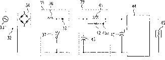
Fig. 1 is a circuit diagram of showing the step-up switching power supply of one embodiment of the invention.
Fig. 2 is the voltage of the action among the embodiment of key diagram 1 and the oscillogram of electric current.
Fig. 3 is a circuit diagram of showing the step-up switching power supply of another embodiment of the present invention.
Fig. 4 shows the circuit diagram of the step-up switching power supply of an embodiment more of the present invention.
Fig. 5 shows the circuit diagram of the step-up switching power supply of an embodiment more of the present invention.
Fig. 6 shows the circuit diagram of the step-up switching power supply of an embodiment more of the present invention.
Fig. 7 shows the circuit diagram of the step-up switching power supply of an embodiment more of the present invention.
Fig. 8 shows the circuit diagram be provided with the example of the multi-form power supply of the circuit of the embodiment of Fig. 1.
Fig. 9 shows the circuit diagram of the step-up switching power supply of an embodiment more of the present invention.
Figure 10 shows the circuit diagram that adopts the switching power unit that possesses the embodiments of the invention that filter circuit is arranged.
Figure 11 is the current waveform figure among the embodiment of Figure 10.
Figure 12 is a circuit diagram of showing the switching power unit that adopts the another embodiment of the present invention that possesses filter circuit.
Figure 13 is a circuit diagram of showing the switching power unit that adopts the another embodiment of the present invention that possesses filter circuit.
Figure 14 is illustrated in the chart that the noise in switching power unit that has used filter circuit of the present invention lowers effect.
The explanation of most preferred embodiment
Below, with reference to the description of drawings embodiments of the invention.Fig. 1 is the figure that shows the 1st embodiment of the present invention, and a terminal of DC power supply 1 is connected on the coil 2 as the 1st magnetic element.The 1st winding 2 is divided into coiler part 2a and coiler part 2b, and the end of the 1st winding part 2a is connected on the power supply 1.The other end of the 1st winding part 2a is connected to output one of capacitor for filter 4 by the 1st diode 3 and extremely goes up.Capacitor 4 is connected on the load resistance 5, provides output to this load resistance 5.At this, coil 2 is divided into coiler part 2a and coiler part 2b means, coil 2 is made of the coiler part 2a and the coiler part 2b that are wound onto on the same magnetic core.
The coiler part 2b of the 1st winding 2, an end are connected on the coiler part 2a, and the other end is by being connected an end of switch element 7 as the 2nd winding 6 of the 2nd magnetic element.The other end of switch element 7 is connected on the other end of power supply 1.
The 2nd capacitor 8 and switch element 7 are connected in parallel, the 2nd capacitor 8, the one utmost point is connected on the 2nd winding 6 by the 2nd diode, also is connected on the coupling part A of the coiler part 2a of the 1st winding 2 and the 1st diode 3 by the 3rd diode 10 and the 3rd capacitor 11.Another utmost point of the 2nd capacitor 8 and switch element 7 together are connected on the above-mentioned another terminal of power supply 1.And then, the 4th diode 12 is set, the coupling part B bypass between the 3rd diode 10 and the 3rd capacitor 11 is connected on the output capacitor for filter 4 in the 3rd capacitor 11 and the 1st diode 3.
The 2nd second tube sheet 9 is so that electric current is a positive direction from the 2nd winding 6 to the 2nd capacitors 8 flow directions, and the 3rd diode 10 is a positive direction with the direction from the 2nd capacitor 8 towards the 3rd capacitors 11.The 4th diode 12 is a positive direction with the direction towards output capacitor for filter 4.Stipulate that the 1st winding 2 is mutual reversed polarity by the coil coiling direction of coiler part 2a, 2b after cutting apart.Coiler part 2a has the inductance more much bigger than coiler part 2b.In addition, coiler part 2b is connected to, and the voltage that takes place at its two ends gives diode 9,10,12 reverses biased.And then, the 3rd capacitor 11, the capacity of its Capacity Ratio the 2nd capacitor 8 is big.
The following action that above-mentioned supply unit is described with reference to Fig. 2.When being in out state of switch element 7 when moment t0 becomes the pass, on the 2nd winding 6, apply and output voltage voltage about equally, the electric current I sw that flows to switch element 7 by the 2nd winding 6 increases point-blank.In this case, the closing simultaneously of voltage Vsw and this switch element 7 that apply of switch element 7 reduced rapidly, but the increase of electric current I sw is slower.Thereby, produce switching loss hardly.
Have only the electric current of switch element 7 to increase, flow through the electric current I of the 1st diode 3
CR1Just reduce, but because the increase of the electric current of switch element 7 is slow, so also make the electric current I that flows through the 1st diode 3
CR1Minimizing speed reduce.Its result can suppress the generation of restoring current.Because this restoring current is little to being difficult to the influence action, so not shown in Fig. 2.
Flow through the electric current I of the 2nd winding 6
L2, certain time after switch element 7 closes and the electric current I sw of switch element 7 increase equally.Begin through sometime from closing of switch element 7, when becoming moment t1, flow through the electric current I of the 2nd winding 6
L2Become and equate from the input current Iin of the coiler part 2a of the 1st winding 2.At this, the 2nd capacitor 8 begins discharge, forms from the resonant circuit of the 2nd capacitor 8 by the 3rd diode the 10, the 3rd capacitor 11, coiler part 2b, the 2nd winding 6 and switch element 7 resonance action beginning.In this state, at the electric current that flows through stack resonance current on from the input current Iin of coiler part 2a on the 2nd winding 6 and the switch element 7.
In the moment that this resonance begins, the 2nd capacitor 8 is charged to output voltage V
o, the current potential V of the coupling part B between the 3rd diode 10 and the 3rd capacitor 11
BWith output voltage V
oEquate.In addition, carve at this moment, the both end voltage of the 3rd capacitor 11 is zero.By resonance the 3rd capacitor 11 is charged the current potential V of coupling part A
ASlowly descend, be applied to the voltage V on the 1st diode 3 thereupon
CR1Slowly increase.Like this, owing to the voltage V that is applied on the 1st diode 3
CR1Increase slow, the voltage that therefore is applied on the 1st diode 3 is suppressed very lowly, even have restoring current to flow in the small time since moment t1, its value is also very little, loses very little.
Because the current potential of resonance coupling part A, B slowly descends the current potential V of coupling part A
AMaximum might drop to-V
oBelow.If the current potential V of coupling part
ADrop to-V
o, then owing on the 1st diode 3, apply 2V
oVoltage, therefore it is high withstand voltage to require diode to have.But, in the present embodiment,, thereby can stop the current potential V of coupling part A because the capacity of Capacity Ratio the 3rd capacitor 11 of the 2nd capacitor 8 is little
ADrop to-V
oIf in more detail, then, drop to-V at the current potential of coupling part A because this constitutes
oBefore, the current potential V of coupling part B
B9 conductings of the 2nd diode are carved in vanishing at this moment, form the 2nd resonant circuit that returns the 2nd diode 9 from the 2nd diode 9 through the 3rd diode the 10, the 3rd capacitor 11, coiler part 2b and the 2nd winding 6.This state produces in moment t2.Produce the result of resonance in the 2nd resonant circuit, the 3rd capacitor 11 further is recharged, the current potential V of coupling part A
AFurther descend, but do not drop to-V
oThereby, can reduce the voltage V that is applied on the 1st diode 3
CR1
If begin by the resonance of the 2nd resonant circuit, then flow through the electric current I of the 2nd winding 6 at moment t2
L2, be the value of resonance current of on input current Iin, having superposeed, and the electric current I sw that flows in switch element 7 becomes with input current Iin and equates from coiler part 2a.The resonance current that flows through the 2nd resonant circuit is in moment t3 vanishing.At this, the resonance current reversed polarity will flow in the opposite direction, but flowing of resonance current stoped by the 2nd diode 9 and the 3rd diode 10.At this, a series of resonance release is carried out and in the past the identical action of step-up switching power supply.
Then, at moment t4, switch element 7 becomes out.Carve at this moment, because the charging voltage of the 2nd capacitor 8 is zero, so flow in this capacitor 8 as charging current from the input current Iin of coiler part 2b.Therefore, the terminal voltage Vsw of switch element 7 slowly rises, and can make the switching losses that produces when switch element 7 is set to out minimum.
Along with the 2nd capacitor 8 is recharged, the current potential V of coupling part A, B
A, V
BRise, at moment t5 voltage V
BWith output voltage V
oEquate.At this moment, on the 2nd winding 6, be applied to the voltage that produces among the 3rd capacitor 11 and the coiler part 2b and, the magnetic energy that is accumulated on the 2nd winding 6 is resetted.Consequent resetting current is discharged into output one side through diode 9,10,12, and resetting current slowly reduces.From the input current Iin of coil 2a, just suitable with the minimizing part of resetting current electric current flows towards the 1st diode 3.At this moment, the 3rd capacitor 11 is in charged state, because the current potential V of coupling part A
ASpecific output voltage V
oLow, so electric current is by the 1st diode 3, and offer output one side through the 4th diode 12 from the 3rd capacitor 11.In Fig. 2, represent to flow through the electric current of the 4th diode 12 with ICR4.In this process, the 3rd capacitor 11 slowly discharges.
Magnetic energy at moment t6 the 2nd winding 6 disappears the resetting current vanishing.Carve at this moment, all flow to coupling part A from the input current Iin of coiler part 2a.At moment t7, the discharge of the 3rd capacitor 11 finishes, because the current potential V of coupling part A
AReach abundant height, therefore the 1st diode 3 conductings all flow to the 1st diode 3 from the input current Iin of coiler part 2a.After this, carry out and in the past the same action of step-up switching power supply.According to condition, the situation that resets and finish at the 3rd capacitor 11 discharges end back the 2nd winding 6 is also arranged, but this does not influence the action of device.
The coiler part 2b of the 1st winding 2 has the voltage that leans against its two ends generation and makes accelerate the effect that resets really the resetting time of the 2nd winding 6.In addition, coiler part 2b, after the end that resets, generation makes diode 9,10,12 become the voltage of reverse biased, and making does not have electric current in these diodes.Thereby, when switch element 7 is closed, can prevent that restoring current from flowing.
In foregoing circuit, the beginning of resonance action and the switching frequency of end and switch element 7 are irrelevant.Thereby the resonance action is not driven driving frequency, even fixed drive frequency, the resonance action is also unaffected.Thereby the control circuit as make the pulse width modulation of device action with fixed frequency can make output voltage stabilizationization.As switch element 7 no matter use which kind of form switching device can, but preferably adopt MOSFET.
Fig. 3 and Fig. 4 are the circuit diagrams of showing the variation of embodiments of the invention shown in Figure 1.In these examples, the position of the 2nd winding 6 does not become, the change in location of the coiler part 2b of the 1st winding 2.That is, in the formation of Fig. 3, coiler part 2b is connected between coiler part 2a and the 1st diode 3.In the embodiment of Fig. 4, coiler part 2b and the 2nd diode 9 are connected in series.In all embodiment, all the embodiment with Fig. 1 is identical with effect in effect.
Fig. 5 is the figure that shows another embodiment of the present invention, is equivalent to exchange mutually in the embodiments of figure 3 the position of the 2nd winding 6 and coiler part 2b.Fig. 6 is the figure that shows another embodiment of the present invention, and coiler part 2b and the 2nd winding 6 are connected in series between coiler part 2a and the 1st diode 3.Fig. 7 is illustrated among the embodiment of Fig. 4, with the evolution of the 2nd winding 6 to the embodiment between coiler part 2a and the 1st diode 3.No matter in which example, all form the 1st resonant circuit and the 2nd resonant circuit, configuration coiler part 2b is identical with the 2nd winding 6 this point on this resonant circuit.
In Fig. 8, show as the input power supply and use AC power 20 to replace the example of DC power supply.The formation of boosted switch part is identical with the embodiment of Fig. 1.AC power 20 is connected on the input filter 21, and the output of this input filter 21 becomes direct current output after being imported into full-wave rectifying circuit 23, and is imported in the circuit shown in Figure 1.
Fig. 9 shows another embodiment of the present invention.In the present embodiment, corresponding components indicate with front embodiment in same symbol.In the present embodiment, DC power supply is that a terminal of power unit 1 is connected on the coil 2 as magnetic element.Coil 2 is made of the 1st winding 2a and the 2nd winding 2b, and each end of these coils 2a, 2b is connected on the power unit 1.At this, it is to say that so-called coil 2 is made of the 1st winding 2a and the 2nd winding 2b, and coil 2 is made of the 1st winding 2a and the 2b coil that are wound onto on the same magnetic core.
The other end of the 1st winding 2a of coil 2 is connected an end of switch element 7, but in the inductance composition of the 1st winding 2a, the inductance composition that the leakage inductance that is called as the 2nd winding 2b magnetic couplings of getting along well is arranged, this leakage inductance can be expressed as the coil or the electric leakage sensor 2c that are connected in series between the 1st winding 2a and the switch element 7 of equal valuely.
The other end of the 2nd winding 2b of coil 2, being connected output one of capacitor for filter 4 by the 1st diode 3 extremely goes up, and in the inductance composition of the 2nd winding 2b, also have and the above-mentioned inductance composition that is called as the leakage inductance of the 1st winding 2a magnetic couplings of getting along well like that, this leakage inductance composition can be expressed as the coil 2d that is connected in series between the 2nd winding 2b and the 1st diode 3 of equal valuely.Capacitor 4 is connected on the load resistance 5, provides output to this load resistance 5.
Be arranged to switch element 7 and the 2nd capacitor 8 is connected in parallel, the 2nd capacitor 8, the one utmost point is connected by the 2nd diode 9 on the 1st winding 2a of coil 2, also is connected the 2nd winding 2b of coil 2 and the coupling part A of the 1st diode 3 by the 3rd diode 10 and the 3rd capacitor 11.Another of the 2nd capacitor 8 extremely gone up and switch element 7 together is connected on the terminal of the above-mentioned other end of power supply 1.And then, the 4th diode 12 is set, it makes coupling part B the 3rd capacitor 11 in parallel and the 1st diode 3 between the 3rd diode 10 and the 3rd capacitor 11 be connected output capacitor for filter 4.
The 2nd diode 9, its forward be set at make electric current from the 1st winding 2a of coil 2 on the direction that the 2nd capacitor 8 flows, the 3rd diode 10, its forward are set at and make on the direction that electric current flows from the 2nd capacitor 8 towards the 3rd capacitors 11.The 4th diode 12, its forward are set on the direction of output capacitor for filter 4.The the 1st, the 2nd winding 2a of coil 2, the coiling direction of 2b are defined as: a side that is connected in power supply 1 becomes same polarity.The 2nd winding 2b has the big coil than the 1st winding 2a.In addition, the 3rd capacitor 11, the capacity of its Capacity Ratio the 2nd capacitor 8 is big.
Below, refer again to the action that Fig. 2 illustrates above-mentioned supply unit.Become the pass if be in out state of switch element 7 at moment t0, then in Fig. 9, apply and output voltage voltage about equally in coil 2 and on coiler part 2c, the 2d of coil 2 equivalences, the electric current I sw that the 1st winding 2a by coil 2 flows on the switch element 7 increases point-blank.In this case, the voltage Vsw that applies of switch element 7 reduces rapidly simultaneously in the pass action with this switch element 7, but the increase of electric current I sw is more slowly.Thereby, produce switching loss hardly.
Have only the increase of the electric current of switch element 7, flow through the electric current I of the 1st diode 3
CR1Just reduce, but because the increase of the electric current of switch element 7 is slow, so flow through the electric current I of the 1st diode 3
CR1Minimizing speed also reduce.Its result can suppress the generation of restoring current.Because this restoring current is little to being difficult to the influence action, so not shown in Fig. 2.
Flow through the electric current I of the 1st winding 2a of coil 2
L2a(in Fig. 2, be expressed as I
L2), certain time after switch element 7 is closed and the electric current I sw of switch element 7 increase equally.Then, if begin then to flow through the electric current I of the 1st winding 2a of coil 2 through becoming t1 constantly sometime from switch element 7 passes
L2aEquate with input current Iin.At this, the 2nd capacitor 8 begins discharge, and through the 1st winding 2a, the 2nd winding 2b of the 3rd diode the 10, the 3rd capacitor 11, coil 2 and the 1st resonant circuit of switch element 7, the resonance action begins from the 2nd capacitor 8 in formation.In this state, in the 1st winding 2a of coil 2 and switch element 7, flow through the electric current of stack resonance current on from the input current Iin of the 1st winding 2a.At the resonance of this generation, be the L-C resonance that carries out between coiler part 2c, the 2d of equivalent representation in coil 2 and the 2nd capacitor 8 and the 3rd capacitor 11.
In this resonance zero hour, the 2nd capacitor 8 is charged to output voltage V
o, the current potential V of the coupling part B between the 3rd diode 10 and the 3rd capacitor 11
BWith output voltage V
oEquate.In addition, at this moment, the both end voltage of the 3rd capacitor 11 is zero.The 3rd capacitor 11 is by resonant charging, the current potential V of coupling part A
ASlowly descend, be applied to the voltage V on the 1st diode 3 thereupon
CR1Slowly increase.Like this, owing to the voltage V that is applied on the 1st diode 3
CR1Increase slow, therefore even have restoring current to flow in the small time since moment t1, its value is also little, loses very little.
If because the current potential of resonance coupling part A, B slowly descends, the current potential V of coupling part A then
AMaximum might drop to-V
oIf the current potential V of coupling part
ADrop to-V
o, then owing on the 1st diode 3, apply 2V
oVoltage, therefore it is high withstand voltage to require diode to have.But, in the present embodiment,, can stop the current potential V of coupling part A because the capacity of Capacity Ratio the 3rd capacitor 11 of the 2nd capacitor 8 is little
ADrop to V
oIf in more detail,, drop to-V at the current potential of coupling part A then owing to adopt this to constitute
oBefore, the current potential V of coupling part B
BVanishing, the 2nd diode 9 conductings this moment form the 2nd resonant circuit that returns the 2nd diode 9 through the 2nd winding 2b and the 1st winding 2a of the 3rd diode the 10, the 3rd capacitor 11, coil 2 from the 2nd diode 9.At the resonance of this generation is the L-C that carries out between coil 2c, the 2d of equivalent representation in coil 2 and the 3rd capacitor 11.This state produces at moment t2.The 2nd resonant circuit produces the structure of resonance, and the 3rd capacitor 11 further is recharged, the current potential V of coupling part A
AFurther descend, but do not drop to-V
oBelow.Thereby, can make the voltage V that is applied on the 1st diode 3
CR1Compare 2V
oLittle.
If begin resonance by the 2nd resonant circuit, then flow through the electric current I of the 1st winding 2a of coil 2 at moment t2
L2a, be the value of stack resonance current on from the input current Iin of power supply 1, and the electric current I sw that flows through switch element 7 becomes with input current and equates.The resonance current that flows through the 2nd resonant circuit is in moment t3 vanishing.At this, the resonance current reversed polarity will flow round about, but flowing of resonance current stoped by the 2nd diode 9 and the 3rd diode 10.At this, a series of resonance release is carried out and the same action of step-up switching power supply in the past.
Then, at moment t4, switch element 7 becomes out.At this moment, because the current potential of the 2nd capacitor 8 is zero, therefore the input current Iin from the 1st winding 2a of coil 2 flows to this capacitor 8 as charging current.Therefore, the terminal voltage Vsw of switch element 7 slowly rises, and the switching losses that produces when switch element 7 is opened is in minimum.
Along with the 2nd capacitor 8 is recharged, the current potential V of coupling part A, B
A, V
BRise, at moment t5 current potential V
BAnd output voltage V
oEquate.At this moment, in coil 2, be equivalent on coiler part 2c, the 2d of coil 2, the suitable voltage of difference of voltage that applies and in the 1st winding 2a of coil 2, produce and the voltage that in the 2nd winding 2b, produces, with the voltage of the 3rd capacitor 11 and, the magnetic energy that is accumulated on coiler part 2c, the 2d is reset.Consequent resetting current is discharged into output one side through diode 9,10,12, and resetting current slowly reduces.From the input current Iin of power supply 1, the minimizing electric current partly that only is equivalent to resetting current is towards the 1st diode 3.At this moment, the 3rd capacitor 11 is in charged state, because the current potential V of coupling part A
ASpecific output voltage V
oLow, therefore, electric current does not pass through the 1st diode 3, and offers output one side from the 3rd capacitor 11 through the 4th diode 12.In Fig. 2, represent to flow through the electric current of the 4th diode 12 with ICR4.In this process, the 3rd capacitor 11 slowly discharges.
Magnetic energy at moment t6 coiler part 2c, 2d disappears the resetting current vanishing.Carve at this moment, from the input current Iin of power supply 1 all towards coupling part A.At moment t7, the discharge of the 3rd capacitor 11 finishes, because the current potential V of coupling part A
AFully high, therefore the 1st diode 3 conductings are all flow through the 1st diode 3 from the input current Iin of power supply 1.After this, carry out and in the past the same action of step-up switching power supply.According to condition, can also discharge at the 3rd capacitor 11 and finish the end that resets of back coiler part 2c, 2d, but this does not influence the action of device.
Owing to the 1st winding 2a that makes coil 2 lacks than the coil of the 2nd winding 2b, therefore the proportional voltage of number of turns difference is applied on coiler part 2a, the 2d therewith, has to accelerate the effect that resets really the resetting time that makes this coiler part 2c, 2d.In addition, with the proportional voltage of difference of the number of turns of the 1st winding 2a of coil 2 and the 2nd winding 2b, because make diode 9,10,12 become reverse biased after finishing resetting, so stop the electric current that in these diodes, flows.Thereby, when switch element 7 is closed, can prevent that restoring current from flowing.
In foregoing circuit, the beginning of resonance action and the switching frequency of end and switch element 7 are irrelevant.Thereby the resonance action is not influenced by driving frequency, and fixedly the resonance action is also unaffected even make driving frequency.Therefore, the control circuit as make the pulse width modulation of device action with fixed frequency can make output voltage stabilizationization.As switch element 7 use any type of switching device can, but preferably adopt MOSFET.
In Fig. 9,, also can adopt the AC power 20 of form shown in Figure 8 to replace DC power supply as the input power supply.The formation of boosted switch part is identical with the embodiment of Fig. 1.AC power 20 is connected on the input filter 21, and the output of this input filter 21 becomes direct current output after being transfused to full-wave rectifying circuit 23, and is imported into circuit shown in Figure 1.
If with reference to Figure 10, then this diagram in switching power unit 30, its power unit 32 can be made of the full-wave rectifying circuit 34 that constitutes with AC power 33 and diode.On power unit 32, connect switching circuit 35.
Two outputs of switching circuit 35 are connected output filtering with the 1st capacitor 40 by filter circuit 39 of the present invention.Filter 39 possesses the inductor 41 as the filter circuit magnetic element on the diode 38 that an end is connected switching circuit 35.Filter circuit resistance 42 is connected in parallel on this inductor 41.Across the filtering circuit capacitor device 43 that is connected with a part that constitutes filter circuit 39 between two outputs of switching circuit 35.By these inductor 41 and filter circuit resistance 42, and the filter circuit 39 that constitutes of filtering circuit capacitor device 43, can form the discrete unit of using with switching circuit 35 and output filtering of the 1st capacitor 40 as the filter circuit magnetic element.
The output of switching circuit 35, the 1st capacitor of using by filter circuit 39 and output filtering 40 is connected DC/DC transducer 44, and the output of this DC/DC transducer 44 is connected on the load 45.
The current waveform of the each several part of switching power unit 30 shown in Figure 10 as shown in figure 11.Figure 11 (a) expression is towards the input current Iin of filter circuit 39, and Figure 11 (b) represents the output current I of filter circuit 39
o, Figure 11 (c) is illustrated in the electric current I that flows in the inductor 41 that constitutes the filter circuit magnetic element
L, Figure 11 (d) is illustrated in the charging current of condenser I that flows in the filtering circuit capacitor device 43
c, Figure 11 (e) is illustrated in the electric current I that flows in the filter circuit 42
R
When the output circuit at moment t0 switching circuit 35 promptly flows to the input current Iin rising of filter circuit 39,, therefore, especially become the reason of the noise of the frequency band that is higher than 10MHz because this input current generally has the following extremely short rise time of 50nS.But in the switching power unit 30 that adopts the above embodiment of the present invention, the input current Iin that this above-mentioned time is short is flowed to the 1st capacitor 40 by inductor 41 preventions, shown in Figure 11 (d), flows into filtering circuit capacitor device 43 as charging current.At this, 42 pairs of resonance of resistance produce braking, play the effect of convergence resonance current.
Input current Iin in case flow into filtering circuit capacitor device 43, after these capacitor 43 chargings, leans against the L-C resonance that produces between inductor 41 and the filter circuit 43, by inductor 41 as output current I
oFlow to the 1st capacitor 40.Its result, the electric current I of inductor 41
LShown in Figure 11 (c), rise lentamente, flow to the output current I of output filtering with the 1st capacitor 40
oAlso slowly rise.
In filtering circuit capacitor device 43, shown in Figure 11 (d), the rise time, short electric current flow through.But,, can make capacity very little so compare with the 1st capacitor 40 because this capacitor 43 can not have the output filter function as the 1st capacitor 40.Thereby this filtering circuit capacitor device 43 is configured near the without any difficulty of switching circuit 35.Its result, can shorten and switching circuit 35 between the pulse current loop that forms, thereby can be with the Min. that is suppressed at of noise.
Flow through the electric current I from filter circuit 39 of output filtering with the 1st capacitor 40
oWaveform, determine by value as inductor 41, resistance 42 and the filtering circuit capacitor device 43 of the composed component of filter circuit 39.By suitably selecting these values, just can prolong output current I from filter circuit 39
oRise time.In order to lower the noise that is higher than in the 10MHz frequency band, from output current I
oRise time promptly from moment t0 to output current I
oBecome the maximum time, more preferably greater than 100nS.
In Figure 11, offer the input current Iin vanishing of filter circuit 39 from switching circuit 35 at moment t1.At this moment the lifting time of input current Iin generally all below 50nS, becomes the reason that noise produces.But, in the switching power unit 1 of this embodiment of the present invention, even because input current Iin vanishing, inductor 41 also will continuously make same electric current flow, so provide electric current from filtering circuit capacitor device 43.Its result produces L-C resonance, output current I between filtering circuit capacitor device 43 and inductor 41
oSlowly reduce.Resistance 42 has played the effect of convergence resonance.Thereby the lifting of inductor current IL becomes shown in Figure 11 (c) slowly, similarly, and the output current I that flows to the 1st capacitor 40
oLifting shown in Figure 11 (d), also become slow.At this moment, in filtering circuit capacitor device 43, shown in Figure 11 (d), flow through the short electric current of lifting time, but because and above-mentioned same reason, suppressed generating noise.
Output current I
oLifting time, the same with the situation of lifting time, determine by value as inductor 41, resistance 42 and the filtering circuit capacitor device 41 of the composed component of filter circuit 39.In order to lower the noise that is higher than the 10MHz frequency band, output current I
oLifting time promptly from moment t1 to output current I
oBecome the minimum time, it is big to can be compared to 100nS most.
Figure 12 shows another embodiment of the present invention.In this embodiment and the part of the embodiment correspondence of Figure 10 indicate same symbol and omit explanation.In the present embodiment, with the resistance 42 of inductor 41 configuration in parallel of filter circuit 39 on be connected the 2nd diode 46.The 2nd diode 46 is connected to positive direction towards the coupling part between inductor 41 and the 1st capacitor 40.In this embodiment, after input current Iin vanishing,, in resistance 42, there is not electric current to flow through because the 2nd diode 46 becomes reverse biased.Its result is because output current I
oWith the electric current I that flows to inductor 41
LEquate, so can make output current I
oLifting time also longer than situation embodiment illustrated in fig. 10.
Figure 13 shows another embodiment of the present invention.In the present embodiment, the 2nd diode 46a with resistance 42 is connected in series is connected on the direction opposite with the situation of embodiment shown in Figure 12.In the present embodiment, can make output current I
oRise time also longer than situation embodiment illustrated in fig. 10.
Figure 10, Figure 12 and filter circuit shown in Figure 13, and if the switching power unit combination among described each embodiment of Fig. 1, Fig. 3 to Fig. 9, then can obtain the effect of significant especially reducing noise.In this case, can use switching circuit 35 among the embodiment of Figure 10, Figure 12 and Figure 13 to replace the switching circuit shown in any one of Fig. 1, Fig. 3 to Fig. 9.
Figure 14 shows the chart that adopts above-mentioned filter circuit to produce the reducing noise effect.In Figure 14, fine line represents not possess the noise level in the switching power unit in the past of filter circuit of the present invention, and heavy line is represented the noise level among the embodiment of Figure 10.In addition, chain-dotted line represents to use the switching circuit of Fig. 1 to replace the noise level of the embodiments of the invention of the switching circuit of embodiment among Figure 10.As we know from the figure, in the embodiment of the invention shown in Figure 10, compare with switching power unit in the past, on the whole the reducing noise level.In addition, in the embodiments of the invention that use switching circuit shown in Figure 1, can further lower the noise that is higher than the 10MHz frequency band.
More than, the present invention is showed among the figure with certain embodiments, and has been described in detail, but the present invention is not limited among these embodiment, under the situation that does not break away from the described spirit of the present invention of claim scope, a lot of changes and correction can be arranged.Thereby the present invention also comprises these possible change and corrections.
Claims (24)
1. step-up switching power supply comprises:
The 1st magnetic element is connected on the end of power unit;
Switching device, an end are connected on above-mentioned the 1st magnetic element, and the other end is connected on the other end of above-mentioned power unit;
Capacitor for filter is connected between the above-mentioned other end of above-mentioned the 1st magnetic element and above-mentioned power unit;
With the 1st diode, be connected between above-mentioned the 1st magnetic element and the above-mentioned capacitor for filter, make its positive direction from above-mentioned power unit by above-mentioned the 1st magnetic element to the making on the charging current of condenser flow direction of above-mentioned capacitor for filter;
And get output from above-mentioned capacitor for filter two ends; It is characterized in that:
Configuration the 2nd magnetic element between above-mentioned switching device and above-mentioned the 1st magnetic element;
Setting and above-mentioned switching device are connected the 2nd capacitor on above-mentioned the 1st magnetic element in parallel, make the 2nd capacitor lean on the current charges from above-mentioned the 1st magnetic element under the state of opening of above-mentioned switching device;
Make the electric current that flows to above-mentioned switching device from above-mentioned the 1st magnetic element at the initial stage of the pass of above-mentioned switching device action by above-mentioned the 2nd magnetic element, thereby the rising of the electric current of above-mentioned switching device is flow through in inhibition;
When the electric current that flows through above-mentioned the 2nd magnetic element increases to setting, between above-mentioned the 1st magnetic element and above-mentioned the 1st diode, form the 1st resonant circuit that the discharging current that makes above-mentioned the 2nd capacitor flows by above-mentioned the 2nd magnetic element and above-mentioned switching device and above-mentioned the 2nd capacitor.
2. step-up switching power supply comprises:
The 1st magnetic element is connected on the end of power unit;
Switching device, an end are connected on above-mentioned the 1st magnetic element, and the other end is connected on the other end of above-mentioned power unit;
Capacitor for filter is connected between the above-mentioned other end of above-mentioned the 1st magnetic element and above-mentioned power unit;
With the 1st diode, be connected between above-mentioned the 1st magnetic element and the above-mentioned capacitor for filter, make its positive direction from above-mentioned power unit by above-mentioned the 1st magnetic element to the making on the charging current of condenser flow direction of above-mentioned capacitor for filter;
And get output from above-mentioned capacitor for filter two ends; It is characterized in that:
On the path of the restoring current that when move the pass of above-mentioned switching device, flows to above-mentioned switching device, dispose the 2nd magnetic element from above-mentioned the 1st diode;
Setting and above-mentioned switching device are connected the 2nd capacitor on above-mentioned the 1st magnetic element in parallel, make the 2nd capacitor lean on the current charges from above-mentioned the 1st magnetic element under the state of opening of above-mentioned switching device;
When the action of the pass of above-mentioned switching device, between above-mentioned the 1st magnetic element and above-mentioned the 1st diode, form the 1st mobile resonant circuit of discharging current that makes above-mentioned the 2nd capacitor by above-mentioned the 2nd magnetic element, above-mentioned switching device, above-mentioned the 2nd capacitor.
3. step-up switching power supply as claimed in claim 1 or 2, it is characterized in that: between above-mentioned the 1st magnetic element and above-mentioned the 2nd capacitor, the 3rd capacitor that configuration is connected with the 2nd capacitors in series, the 3rd capacitor is by the charging of the resonance current in above-mentioned the 1st resonant circuit, setting makes above-mentioned the 2nd magnetic element be connected bypass circuit between above-mentioned the 2nd capacitor and above-mentioned the 3rd capacitor, be provided with on this bypass circuit make its forward from above-mentioned the 2nd magnetic element towards the above-mentioned the 2nd and the direction of the 3rd capacitor on the 2nd diode, when because the charging voltage of discharge the 2nd capacitor of above-mentioned the 2nd capacitor when dropping to setting, above-mentioned the 2nd diode current flow, between above-mentioned the 1st magnetic element and above-mentioned the 1st diode, form the 2nd resonant circuit that the discharging current that makes above-mentioned the 3rd capacitor flows through by above-mentioned the 2nd magnetic element and above-mentioned the 2nd diode and above-mentioned the 3rd capacitor.
4. step-up switching power supply as claimed in claim 3 is characterized in that: between above-mentioned the 2nd capacitor and above-mentioned the 3rd capacitor, be provided with the 3rd diode, its forward is arranged on and makes on the direction that flows from the electric current of above-mentioned the 2nd diode.
5. step-up switching power supply as claimed in claim 4 is characterized in that: be provided with the 4th diode, it makes the current bypass from above-mentioned the 3rd diode flow towards above-mentioned capacitor for filter in above-mentioned the 3rd capacitor and above-mentioned the 1st diode.
6. as each described step-up switching power supply of claim 3 to 5, it is characterized in that: above-mentioned the 1st magnetic element is divided into 2 parts, magnetic part after cutting apart is connected to above-mentioned power unit, and connects another magnetic part it is comprised in above-mentioned the 2nd resonant circuit.
7. step-up switching power supply as claimed in claim 5, it is characterized in that: above-mentioned the 1st magnetic element is divided into 2 parts, magnetic part after cutting apart is connected on the above-mentioned power unit, another magnetic part is under the state of opening of above-mentioned switching device, and the polarity that becomes reverse biased with above-mentioned the 2nd, the 3rd, the 4th diode is connected in above-mentioned the 2nd resonant circuit.
8. as claim 4 or 5 described step-up switching power supplies, it is characterized in that: above-mentioned the 3rd capacitor volume is bigger than above-mentioned the 2nd capacitor volume.
9. step-up switching power supply comprises:
The 1st magnetic element is connected on the end of power unit;
Switching device, an end are connected on above-mentioned the 1st magnetic element, and the other end is connected on the other end of above-mentioned power unit;
Capacitor for filter is connected between the above-mentioned other end of above-mentioned the 1st magnetic element and above-mentioned power unit;
With the 1st diode, be connected between above-mentioned the 1st magnetic element and the above-mentioned capacitor for filter, its positive direction from above-mentioned power unit by above-mentioned the 1st magnetic element to the making on the charging current of condenser flow direction of above-mentioned capacitor for filter;
And get output from above-mentioned capacitor for filter two ends; It is characterized in that:
Above-mentioned magnetic element possesses the 1st winding and the 2nd winding, one end of above-mentioned the 1st winding is connected on the above-mentioned switching device, the other end is connected on the above-mentioned power unit, an end of above-mentioned the 2nd winding is connected on the above-mentioned diode, the other end is connected on the above-mentioned power unit;
When above-mentioned switching device is opened, mobile in above-mentioned the 2nd winding of above-mentioned magnetic element from the electric current of above-mentioned power unit, when above-mentioned switch closes, mobile in above-mentioned the 1st winding of above-mentioned magnetic coil from the electric current of above-mentioned power unit;
Be connected in series initial stage of the pass action that is above-mentioned switching device of above-mentioned the 1st winding and above-mentioned the 2nd winding flows to from above-mentioned the 1st diode on the path of restoring current of above-mentioned switching device, and the initial stage that is suppressed at the action of above-mentioned pass is flow through the rising of the electric current of above-mentioned switching device;
Be provided with and above-mentioned switching device is connected in the 2nd capacitor on above-mentioned the 1st magnetic element in parallel, make the 2nd capacitor under the state of opening of above-mentioned switching device by current charges from above-mentioned the 1st winding;
When the electric current of above-mentioned the 1st winding that flows through above-mentioned magnetic element is increased to setting, form the 1st mobile resonant circuit of discharging current that makes above-mentioned the 2nd capacitor by above-mentioned the 1st winding of above-mentioned magnetic element, above-mentioned switching device, above-mentioned the 2nd capacitor.
10. step-up switching power supply as claimed in claim 9, it is characterized in that: between above-mentioned the 2nd winding and above-mentioned the 2nd capacitor of above-mentioned magnetic element, the 3rd capacitor that configuration is connected with the 2nd capacitors in series, make the 3rd capacitor by the charging of the resonance current in above-mentioned the 1st resonant circuit, above-mentioned the 1st winding with above-mentioned magnetic element is set is connected bypass circuit between above-mentioned the 2nd capacitor and above-mentioned the 3rd capacitor, configuration the 2nd diode on this bypass circuit, make its forward from above-mentioned the 1st winding towards the above-mentioned the 2nd and the direction of the 3rd capacitor on, when because the charging voltage of discharge the 2nd capacitor of above-mentioned the 2nd capacitor when dropping to setting, above-mentioned the 2nd diode current flow forms the 2nd resonant circuit that the discharging current that makes above-mentioned the 3rd capacitor flows by above-mentioned magnetic element and above-mentioned the 2nd diode and above-mentioned the 3rd capacitor.
11. step-up switching power supply as claimed in claim 10 is characterized in that: between above-mentioned the 2nd capacitor and above-mentioned the 3rd capacitor, it is the 3rd diode of forward that setting makes from the direction of current flow of above-mentioned the 2nd diode.
12. step-up switching power supply as claimed in claim 11 is characterized in that: be provided with the 4th diode, it makes the current bypass from above-mentioned the 3rd diode lead to above-mentioned capacitor for filter behind above-mentioned the 3rd capacitor and above-mentioned the 1st diode.
13. each the described step-up switching power supply as claim 10 to 12 is characterized in that: the number of turns of above-mentioned the 2nd winding of above-mentioned the 1st ratio of winding of above-mentioned magnetic element is few.
14. as claim 12 or 13 described step-up switching power supplies, it is characterized in that: above-mentioned the 3rd capacitor volume is bigger than above-mentioned the 2nd capacitor volume.
15. a switching power unit comprises:
Switching circuit, be connected the switch element between the other end of the 1st magnetic element, another output that is connected above-mentioned power unit and above-mentioned the 1st magnetic element on the output of power unit by an end, and the diode that is connected on above-mentioned the 1st magnetic element and the above-mentioned switch element constitutes;
With the 1st capacitor, be connected on the output of said switching circuit, make the output smoothingization of said switching circuit; It is characterized in that:
Possesses the filter circuit on the output of the said switching circuit of being connected;
Above-mentioned filter circuit, be connected the filter circuit magnetic element of an end of above-mentioned filtering circuit capacitor device by the filtering circuit capacitor device on the output that is connected said switching circuit, an end, and the filter circuit resistance that is connected in parallel with above-mentioned filter circuit magnetic element constitutes, and the other end of the other end of above-mentioned filtering circuit capacitor device and above-mentioned filter circuit magnetic element is connected to the two ends of above-mentioned the 1st capacitor.
16. step-up switching power supply as claimed in claim 15 is characterized in that:
Said switching circuit possesses, the 2nd magnetic element, and it is configured between above-mentioned switch element and above-mentioned the 1st magnetic element; With the 2nd capacitor, itself and above-mentioned switch element are connected in parallel on above-mentioned the 1st magnetic element; Above-mentioned the 2nd capacitor is under the state of opening of above-mentioned switch element, by current charges from the 1st magnetic element, the initial stage of moving in the pass of above-mentioned switch element makes from above-mentioned the 1st magnetic element and flows to the electric current of above-mentioned switch element by above-mentioned the 2nd magnetic element, the rising of the electric current of above-mentioned switch element is flow through in inhibition, when the electric current that flows through above-mentioned the 2nd magnetic element reaches setting, between above-mentioned the 1st magnetic element and above-mentioned diode, form the resonant circuit that the discharging current that makes above-mentioned the 2nd capacitor flows by above-mentioned the 2nd magnetic element and above-mentioned switch element and above-mentioned the 2nd capacitor.
17. step-up switching power supply as claimed in claim 15 is characterized in that:
Said switching circuit possesses, and the 2nd magnetic element is configured on the path of the restoring current that flows to above-mentioned switch element when the action of the pass of above-mentioned switch element from above-mentioned diode; With the 2nd capacitor, be connected in parallel on above-mentioned the 1st magnetic element with above-mentioned switch element; Above-mentioned the 2nd capacitor by from the current charges of above-mentioned the 1st magnetic element, makes the mobile resonant circuit of discharging current of above-mentioned the 2nd capacitor when forming when the action of the pass of above-mentioned switch element by above-mentioned the 2nd magnetic element and above-mentioned switch element and above-mentioned the 2nd capacitor between above-mentioned the 1st magnetic element and the above-mentioned diode under the state of opening of above-mentioned switch element.
18. any described switching power unit as claim 15 to 17 is characterized in that: the 2nd diode and above-mentioned filter circuit resistive element are connected in series, and are connected in parallel with this filter circuit magnetic element.
19. step-up switching power supply as claimed in claim 18 is characterized in that: above-mentioned the 2nd diode is connected to its forward, and another is distolateral towards above-mentioned filtering circuit capacitor device above-mentioned.
20. step-up switching power supply as claimed in claim 18 is characterized in that: above-mentioned the 2nd diode is connected to its forward above-mentioned distolateral towards above-mentioned filtering circuit capacitor device.
21. a filter is to be used for the filter circuit that the reducing noise of switching power unit is used, and comprises
Switching circuit, be connected the switch element between the other end of the 1st magnetic element of an output of power unit, another output that is connected above-mentioned power unit and above-mentioned the 1st magnetic element by an end, and the diode that is connected on above-mentioned the 1st magnetic element and the above-mentioned switch element constitutes;
With the 1st capacitor, be connected on the output of said switching circuit, make the output smoothingization of said switching circuit, it is characterized in that:
Be connected the filter circuit magnetic element of an end of above-mentioned filtering circuit capacitor device by the filtering circuit capacitor device on the output that is connected said switching circuit, an end, and constitute with filter circuit resistance that above-mentioned filter circuit magnetic element is connected in parallel,
The other end of the other end of above-mentioned filtering circuit capacitor device and above-mentioned filter circuit magnetic element is connected to the two ends of above-mentioned the 1st capacitor.
22. filter circuit as claimed in claim 21 is characterized in that: the 2nd diode and above-mentioned filter circuit resistive element are connected in series, and are connected in parallel with above-mentioned filter circuit magnetic element.
23. filter circuit as claimed in claim 22 is characterized in that: above-mentioned the 2nd diode is connected to forward, and another is distolateral towards above-mentioned filtering circuit capacitor device above-mentioned.
24. filter circuit as claimed in claim 22 is characterized in that: above-mentioned the 2nd diode is connected to forward above-mentioned distolateral towards above-mentioned filter circuit.
Applications Claiming Priority (9)
| Application Number | Priority Date | Filing Date | Title |
|---|---|---|---|
| JP26368/97 | 1997-02-10 | ||
| JP2636897 | 1997-02-10 | ||
| JP26368/1997 | 1997-02-10 | ||
| JP16681297 | 1997-06-24 | ||
| JP166812/97 | 1997-06-24 | ||
| JP166812/1997 | 1997-06-24 | ||
| JP16865097 | 1997-06-25 | ||
| JP168650/1997 | 1997-06-25 | ||
| JP168650/97 | 1997-06-25 |
Publications (2)
| Publication Number | Publication Date |
|---|---|
| CN1219299A CN1219299A (en) | 1999-06-09 |
| CN1065085C true CN1065085C (en) | 2001-04-25 |
Family
ID=27285371
Family Applications (1)
| Application Number | Title | Priority Date | Filing Date |
|---|---|---|---|
| CN988002485A Expired - Fee Related CN1065085C (en) | 1997-02-10 | 1998-01-27 | Step-up switching power supply |
Country Status (5)
| Country | Link |
|---|---|
| EP (1) | EP0910158A4 (en) |
| JP (2) | JP3285590B2 (en) |
| CN (1) | CN1065085C (en) |
| TW (1) | TW366626B (en) |
| WO (1) | WO1998035432A1 (en) |
Families Citing this family (21)
| Publication number | Priority date | Publication date | Assignee | Title |
|---|---|---|---|---|
| EP0988925B1 (en) * | 1998-09-12 | 2001-12-05 | Urs Bucher | Workpiece carrier with energy storing device |
| JP3425418B2 (en) * | 2000-09-20 | 2003-07-14 | ティーディーケイ株式会社 | Step-up switching power supply |
| FR2821996B1 (en) | 2001-03-09 | 2003-06-13 | St Microelectronics Sa | CIRCUIT FOR SWITCHING A CUT-OUT CONVERTER |
| JP3791350B2 (en) * | 2001-05-28 | 2006-06-28 | 松下電工株式会社 | Power supply |
| US6926288B2 (en) * | 2003-06-02 | 2005-08-09 | Bose Corporation | Electromagnetic interference filter |
| JP4806323B2 (en) * | 2006-10-11 | 2011-11-02 | 本田技研工業株式会社 | DC-DC converter |
| JP4806325B2 (en) * | 2006-10-11 | 2011-11-02 | 本田技研工業株式会社 | DC-DC converter |
| US7768243B2 (en) * | 2007-02-02 | 2010-08-03 | Stmicroelectronics S.A. | Aid for the switching of a switched-mode converter |
| US7911758B2 (en) * | 2008-05-13 | 2011-03-22 | Automatic Switch Company | Low power solenoid control system and method |
| JP5721440B2 (en) * | 2008-12-26 | 2015-05-20 | 三菱電機株式会社 | LED lighting device and LED lighting device for headlamp |
| JP5358387B2 (en) * | 2009-10-06 | 2013-12-04 | 日立アプライアンス株式会社 | Power supply |
| JP2011239545A (en) * | 2010-05-10 | 2011-11-24 | Sanken Electric Co Ltd | Dc-dc converter |
| JP5743269B2 (en) * | 2011-07-11 | 2015-07-01 | 富士電機株式会社 | Buck-boost converter |
| JP5885203B2 (en) * | 2012-05-31 | 2016-03-15 | 富士電機株式会社 | Buck-boost switching power supply circuit |
| JP6132086B2 (en) * | 2013-03-12 | 2017-05-24 | 富士電機株式会社 | DC voltage conversion circuit |
| EP2782235A1 (en) * | 2013-03-21 | 2014-09-24 | Mitsubishi Electric R&D Centre Europe B.V. | Converter composed of at least a first and a second switches and a snubber circuit which protects the second switch |
| CN103595248B (en) * | 2013-11-21 | 2015-12-30 | 中国人民解放军重庆通信学院 | A kind of Sofe Switch Boost topology circuit |
| CN103944383B (en) * | 2014-04-14 | 2016-10-05 | 深圳市航嘉驰源电气股份有限公司 | A kind of Boost |
| CN105471257A (en) * | 2015-12-24 | 2016-04-06 | 特变电工西安电气科技有限公司 | Novel interleaved boost soft-switch circuit |
| CN105720817A (en) * | 2016-04-25 | 2016-06-29 | 佛山市新光宏锐电源设备有限公司 | PFC soft switching circuit of BOOST circuit |
| CN113258755B (en) * | 2020-02-13 | 2022-07-26 | 宏碁股份有限公司 | Boost converter |
Citations (2)
| Publication number | Priority date | Publication date | Assignee | Title |
|---|---|---|---|---|
| JPH01311862A (en) * | 1988-06-08 | 1989-12-15 | Hitachi Lighting Ltd | Switching power circuit |
| JPH08308219A (en) * | 1994-11-01 | 1996-11-22 | Sanken Electric Co Ltd | Chopper type dc-dc converter |
Family Cites Families (4)
| Publication number | Priority date | Publication date | Assignee | Title |
|---|---|---|---|---|
| JPS60226774A (en) * | 1984-04-23 | 1985-11-12 | Amada Co Ltd | Burst wave smoothing circuit |
| GB8816774D0 (en) * | 1988-07-14 | 1988-08-17 | Bsr Int Plc | Power supplies |
| US5144204A (en) * | 1991-05-28 | 1992-09-01 | General Electric Company | Tapped-inductor boost convertor for operating a gas discharge lamp |
| US5543704A (en) * | 1994-06-08 | 1996-08-06 | Telefonaktiebolaget Lm Ericsson | Pulse width modulated DC-to-DC boost converter |
-
1998
- 1998-01-27 JP JP52454098A patent/JP3285590B2/en not_active Expired - Lifetime
- 1998-01-27 EP EP98900742A patent/EP0910158A4/en not_active Withdrawn
- 1998-01-27 WO PCT/JP1998/000308 patent/WO1998035432A1/en not_active Application Discontinuation
- 1998-01-27 CN CN988002485A patent/CN1065085C/en not_active Expired - Fee Related
- 1998-02-07 TW TW087101645A patent/TW366626B/en active
-
2000
- 2000-04-24 JP JP2000122137A patent/JP2000324811A/en not_active Withdrawn
Patent Citations (2)
| Publication number | Priority date | Publication date | Assignee | Title |
|---|---|---|---|---|
| JPH01311862A (en) * | 1988-06-08 | 1989-12-15 | Hitachi Lighting Ltd | Switching power circuit |
| JPH08308219A (en) * | 1994-11-01 | 1996-11-22 | Sanken Electric Co Ltd | Chopper type dc-dc converter |
Also Published As
| Publication number | Publication date |
|---|---|
| EP0910158A1 (en) | 1999-04-21 |
| CN1219299A (en) | 1999-06-09 |
| WO1998035432A1 (en) | 1998-08-13 |
| EP0910158A4 (en) | 2000-05-10 |
| JP2000324811A (en) | 2000-11-24 |
| TW366626B (en) | 1999-08-11 |
| JP3285590B2 (en) | 2002-05-27 |
Similar Documents
| Publication | Publication Date | Title |
|---|---|---|
| CN1065085C (en) | Step-up switching power supply | |
| CN100337391C (en) | Switching power supply apparatus | |
| CN1232021C (en) | Method for controlling DC-DC converter | |
| KR101304816B1 (en) | Charge pump circuit and operation control method thereof | |
| CN1042686C (en) | Power source device | |
| CN1274084C (en) | Charge pump circuit | |
| CN1041984C (en) | Pulse width modulated dc-to-dc boost converter | |
| CN1139175C (en) | DC-AC exchanger | |
| KR101675846B1 (en) | Dc-dc boost converter circuit and method for driving the same | |
| CN1910807A (en) | Switching noise filter circuit for DC-DC converter | |
| CN1116369A (en) | Power source device | |
| CN1976191A (en) | Switching regulator, and circuit and method for controlling same | |
| CN1716747A (en) | DC-DC converter | |
| CN1238958C (en) | Switch power supply device | |
| CN1186874C (en) | Control method of charging exciting circuit | |
| JP2005224058A (en) | Dc/dc converter and program | |
| CN1841900A (en) | Switching regulator circuit | |
| CN1866711A (en) | Constant-voltage circuit, semiconductor apparatus including constant-voltage circuit, and control method of constant-voltage circuit | |
| CN1585247A (en) | Switching electric source device | |
| CN1117377A (en) | Electric dust collector | |
| CN1393050A (en) | Step-up switching power supply device | |
| CN1969446A (en) | DC-DC converter and power supply device | |
| CN1274077C (en) | Synchronous rectification circuit for flyback converter | |
| CN1238952C (en) | Low-loss DC/DC booster circuit | |
| CN1638252A (en) | Power supply unit and portable apparatus utilizing the same |
Legal Events
| Date | Code | Title | Description |
|---|---|---|---|
| C06 | Publication | ||
| PB01 | Publication | ||
| C10 | Entry into substantive examination | ||
| SE01 | Entry into force of request for substantive examination | ||
| C14 | Grant of patent or utility model | ||
| GR01 | Patent grant | ||
| C19 | Lapse of patent right due to non-payment of the annual fee | ||
| CF01 | Termination of patent right due to non-payment of annual fee |