CN106487264B - Semiconductor integrated circuit device for driving power semiconductor device and electronic device - Google Patents
Semiconductor integrated circuit device for driving power semiconductor device and electronic device Download PDFInfo
- Publication number
- CN106487264B CN106487264B CN201610670696.8A CN201610670696A CN106487264B CN 106487264 B CN106487264 B CN 106487264B CN 201610670696 A CN201610670696 A CN 201610670696A CN 106487264 B CN106487264 B CN 106487264B
- Authority
- CN
- China
- Prior art keywords
- circuit
- current
- terminal
- voltage
- power semiconductor
- Prior art date
- Legal status (The legal status is an assumption and is not a legal conclusion. Google has not performed a legal analysis and makes no representation as to the accuracy of the status listed.)
- Active
Links
Images


Classifications
-
- H—ELECTRICITY
- H02—GENERATION; CONVERSION OR DISTRIBUTION OF ELECTRIC POWER
- H02P—CONTROL OR REGULATION OF ELECTRIC MOTORS, ELECTRIC GENERATORS OR DYNAMO-ELECTRIC CONVERTERS; CONTROLLING TRANSFORMERS, REACTORS OR CHOKE COILS
- H02P27/00—Arrangements or methods for the control of AC motors characterised by the kind of supply voltage
- H02P27/04—Arrangements or methods for the control of AC motors characterised by the kind of supply voltage using variable-frequency supply voltage, e.g. inverter or converter supply voltage
- H02P27/06—Arrangements or methods for the control of AC motors characterised by the kind of supply voltage using variable-frequency supply voltage, e.g. inverter or converter supply voltage using dc to ac converters or inverters
- H02P27/08—Arrangements or methods for the control of AC motors characterised by the kind of supply voltage using variable-frequency supply voltage, e.g. inverter or converter supply voltage using dc to ac converters or inverters with pulse width modulation
-
- G—PHYSICS
- G01—MEASURING; TESTING
- G01R—MEASURING ELECTRIC VARIABLES; MEASURING MAGNETIC VARIABLES
- G01R19/00—Arrangements for measuring currents or voltages or for indicating presence or sign thereof
- G01R19/165—Indicating that current or voltage is either above or below a predetermined value or within or outside a predetermined range of values
-
- H—ELECTRICITY
- H02—GENERATION; CONVERSION OR DISTRIBUTION OF ELECTRIC POWER
- H02M—APPARATUS FOR CONVERSION BETWEEN AC AND AC, BETWEEN AC AND DC, OR BETWEEN DC AND DC, AND FOR USE WITH MAINS OR SIMILAR POWER SUPPLY SYSTEMS; CONVERSION OF DC OR AC INPUT POWER INTO SURGE OUTPUT POWER; CONTROL OR REGULATION THEREOF
- H02M7/00—Conversion of ac power input into dc power output; Conversion of dc power input into ac power output
- H02M7/42—Conversion of dc power input into ac power output without possibility of reversal
- H02M7/44—Conversion of dc power input into ac power output without possibility of reversal by static converters
- H02M7/48—Conversion of dc power input into ac power output without possibility of reversal by static converters using discharge tubes with control electrode or semiconductor devices with control electrode
- H02M7/53—Conversion of dc power input into ac power output without possibility of reversal by static converters using discharge tubes with control electrode or semiconductor devices with control electrode using devices of a triode or transistor type requiring continuous application of a control signal
- H02M7/537—Conversion of dc power input into ac power output without possibility of reversal by static converters using discharge tubes with control electrode or semiconductor devices with control electrode using devices of a triode or transistor type requiring continuous application of a control signal using semiconductor devices only, e.g. single switched pulse inverters
- H02M7/5387—Conversion of dc power input into ac power output without possibility of reversal by static converters using discharge tubes with control electrode or semiconductor devices with control electrode using devices of a triode or transistor type requiring continuous application of a control signal using semiconductor devices only, e.g. single switched pulse inverters in a bridge configuration
-
- B—PERFORMING OPERATIONS; TRANSPORTING
- B60—VEHICLES IN GENERAL
- B60L—PROPULSION OF ELECTRICALLY-PROPELLED VEHICLES; SUPPLYING ELECTRIC POWER FOR AUXILIARY EQUIPMENT OF ELECTRICALLY-PROPELLED VEHICLES; ELECTRODYNAMIC BRAKE SYSTEMS FOR VEHICLES IN GENERAL; MAGNETIC SUSPENSION OR LEVITATION FOR VEHICLES; MONITORING OPERATING VARIABLES OF ELECTRICALLY-PROPELLED VEHICLES; ELECTRIC SAFETY DEVICES FOR ELECTRICALLY-PROPELLED VEHICLES
- B60L15/00—Methods, circuits, or devices for controlling the traction-motor speed of electrically-propelled vehicles
- B60L15/02—Methods, circuits, or devices for controlling the traction-motor speed of electrically-propelled vehicles characterised by the form of the current used in the control circuit
- B60L15/08—Methods, circuits, or devices for controlling the traction-motor speed of electrically-propelled vehicles characterised by the form of the current used in the control circuit using pulses
-
- B—PERFORMING OPERATIONS; TRANSPORTING
- B60—VEHICLES IN GENERAL
- B60L—PROPULSION OF ELECTRICALLY-PROPELLED VEHICLES; SUPPLYING ELECTRIC POWER FOR AUXILIARY EQUIPMENT OF ELECTRICALLY-PROPELLED VEHICLES; ELECTRODYNAMIC BRAKE SYSTEMS FOR VEHICLES IN GENERAL; MAGNETIC SUSPENSION OR LEVITATION FOR VEHICLES; MONITORING OPERATING VARIABLES OF ELECTRICALLY-PROPELLED VEHICLES; ELECTRIC SAFETY DEVICES FOR ELECTRICALLY-PROPELLED VEHICLES
- B60L3/00—Electric devices on electrically-propelled vehicles for safety purposes; Monitoring operating variables, e.g. speed, deceleration or energy consumption
- B60L3/0023—Detecting, eliminating, remedying or compensating for drive train abnormalities, e.g. failures within the drive train
- B60L3/0061—Detecting, eliminating, remedying or compensating for drive train abnormalities, e.g. failures within the drive train relating to electrical machines
-
- B—PERFORMING OPERATIONS; TRANSPORTING
- B60—VEHICLES IN GENERAL
- B60L—PROPULSION OF ELECTRICALLY-PROPELLED VEHICLES; SUPPLYING ELECTRIC POWER FOR AUXILIARY EQUIPMENT OF ELECTRICALLY-PROPELLED VEHICLES; ELECTRODYNAMIC BRAKE SYSTEMS FOR VEHICLES IN GENERAL; MAGNETIC SUSPENSION OR LEVITATION FOR VEHICLES; MONITORING OPERATING VARIABLES OF ELECTRICALLY-PROPELLED VEHICLES; ELECTRIC SAFETY DEVICES FOR ELECTRICALLY-PROPELLED VEHICLES
- B60L3/00—Electric devices on electrically-propelled vehicles for safety purposes; Monitoring operating variables, e.g. speed, deceleration or energy consumption
- B60L3/12—Recording operating variables ; Monitoring of operating variables
-
- B—PERFORMING OPERATIONS; TRANSPORTING
- B60—VEHICLES IN GENERAL
- B60L—PROPULSION OF ELECTRICALLY-PROPELLED VEHICLES; SUPPLYING ELECTRIC POWER FOR AUXILIARY EQUIPMENT OF ELECTRICALLY-PROPELLED VEHICLES; ELECTRODYNAMIC BRAKE SYSTEMS FOR VEHICLES IN GENERAL; MAGNETIC SUSPENSION OR LEVITATION FOR VEHICLES; MONITORING OPERATING VARIABLES OF ELECTRICALLY-PROPELLED VEHICLES; ELECTRIC SAFETY DEVICES FOR ELECTRICALLY-PROPELLED VEHICLES
- B60L50/00—Electric propulsion with power supplied within the vehicle
- B60L50/50—Electric propulsion with power supplied within the vehicle using propulsion power supplied by batteries or fuel cells
- B60L50/51—Electric propulsion with power supplied within the vehicle using propulsion power supplied by batteries or fuel cells characterised by AC-motors
-
- B—PERFORMING OPERATIONS; TRANSPORTING
- B60—VEHICLES IN GENERAL
- B60L—PROPULSION OF ELECTRICALLY-PROPELLED VEHICLES; SUPPLYING ELECTRIC POWER FOR AUXILIARY EQUIPMENT OF ELECTRICALLY-PROPELLED VEHICLES; ELECTRODYNAMIC BRAKE SYSTEMS FOR VEHICLES IN GENERAL; MAGNETIC SUSPENSION OR LEVITATION FOR VEHICLES; MONITORING OPERATING VARIABLES OF ELECTRICALLY-PROPELLED VEHICLES; ELECTRIC SAFETY DEVICES FOR ELECTRICALLY-PROPELLED VEHICLES
- B60L7/00—Electrodynamic brake systems for vehicles in general
- B60L7/10—Dynamic electric regenerative braking
- B60L7/14—Dynamic electric regenerative braking for vehicles propelled by ac motors
-
- H—ELECTRICITY
- H02—GENERATION; CONVERSION OR DISTRIBUTION OF ELECTRIC POWER
- H02P—CONTROL OR REGULATION OF ELECTRIC MOTORS, ELECTRIC GENERATORS OR DYNAMO-ELECTRIC CONVERTERS; CONTROLLING TRANSFORMERS, REACTORS OR CHOKE COILS
- H02P27/00—Arrangements or methods for the control of AC motors characterised by the kind of supply voltage
- H02P27/04—Arrangements or methods for the control of AC motors characterised by the kind of supply voltage using variable-frequency supply voltage, e.g. inverter or converter supply voltage
- H02P27/06—Arrangements or methods for the control of AC motors characterised by the kind of supply voltage using variable-frequency supply voltage, e.g. inverter or converter supply voltage using dc to ac converters or inverters
- H02P27/08—Arrangements or methods for the control of AC motors characterised by the kind of supply voltage using variable-frequency supply voltage, e.g. inverter or converter supply voltage using dc to ac converters or inverters with pulse width modulation
- H02P27/085—Arrangements or methods for the control of AC motors characterised by the kind of supply voltage using variable-frequency supply voltage, e.g. inverter or converter supply voltage using dc to ac converters or inverters with pulse width modulation wherein the PWM mode is adapted on the running conditions of the motor, e.g. the switching frequency
-
- H—ELECTRICITY
- H02—GENERATION; CONVERSION OR DISTRIBUTION OF ELECTRIC POWER
- H02P—CONTROL OR REGULATION OF ELECTRIC MOTORS, ELECTRIC GENERATORS OR DYNAMO-ELECTRIC CONVERTERS; CONTROLLING TRANSFORMERS, REACTORS OR CHOKE COILS
- H02P29/00—Arrangements for regulating or controlling electric motors, appropriate for both AC and DC motors
- H02P29/02—Providing protection against overload without automatic interruption of supply
- H02P29/032—Preventing damage to the motor, e.g. setting individual current limits for different drive conditions
-
- H—ELECTRICITY
- H03—ELECTRONIC CIRCUITRY
- H03K—PULSE TECHNIQUE
- H03K17/00—Electronic switching or gating, i.e. not by contact-making and –breaking
- H03K17/08—Modifications for protecting switching circuit against overcurrent or overvoltage
- H03K17/082—Modifications for protecting switching circuit against overcurrent or overvoltage by feedback from the output to the control circuit
- H03K17/0828—Modifications for protecting switching circuit against overcurrent or overvoltage by feedback from the output to the control circuit in composite switches
-
- B—PERFORMING OPERATIONS; TRANSPORTING
- B60—VEHICLES IN GENERAL
- B60L—PROPULSION OF ELECTRICALLY-PROPELLED VEHICLES; SUPPLYING ELECTRIC POWER FOR AUXILIARY EQUIPMENT OF ELECTRICALLY-PROPELLED VEHICLES; ELECTRODYNAMIC BRAKE SYSTEMS FOR VEHICLES IN GENERAL; MAGNETIC SUSPENSION OR LEVITATION FOR VEHICLES; MONITORING OPERATING VARIABLES OF ELECTRICALLY-PROPELLED VEHICLES; ELECTRIC SAFETY DEVICES FOR ELECTRICALLY-PROPELLED VEHICLES
- B60L2210/00—Converter types
- B60L2210/40—DC to AC converters
-
- B—PERFORMING OPERATIONS; TRANSPORTING
- B60—VEHICLES IN GENERAL
- B60L—PROPULSION OF ELECTRICALLY-PROPELLED VEHICLES; SUPPLYING ELECTRIC POWER FOR AUXILIARY EQUIPMENT OF ELECTRICALLY-PROPELLED VEHICLES; ELECTRODYNAMIC BRAKE SYSTEMS FOR VEHICLES IN GENERAL; MAGNETIC SUSPENSION OR LEVITATION FOR VEHICLES; MONITORING OPERATING VARIABLES OF ELECTRICALLY-PROPELLED VEHICLES; ELECTRIC SAFETY DEVICES FOR ELECTRICALLY-PROPELLED VEHICLES
- B60L2240/00—Control parameters of input or output; Target parameters
- B60L2240/40—Drive Train control parameters
- B60L2240/42—Drive Train control parameters related to electric machines
- B60L2240/427—Voltage
-
- B—PERFORMING OPERATIONS; TRANSPORTING
- B60—VEHICLES IN GENERAL
- B60L—PROPULSION OF ELECTRICALLY-PROPELLED VEHICLES; SUPPLYING ELECTRIC POWER FOR AUXILIARY EQUIPMENT OF ELECTRICALLY-PROPELLED VEHICLES; ELECTRODYNAMIC BRAKE SYSTEMS FOR VEHICLES IN GENERAL; MAGNETIC SUSPENSION OR LEVITATION FOR VEHICLES; MONITORING OPERATING VARIABLES OF ELECTRICALLY-PROPELLED VEHICLES; ELECTRIC SAFETY DEVICES FOR ELECTRICALLY-PROPELLED VEHICLES
- B60L2240/00—Control parameters of input or output; Target parameters
- B60L2240/40—Drive Train control parameters
- B60L2240/42—Drive Train control parameters related to electric machines
- B60L2240/429—Current
-
- G—PHYSICS
- G01—MEASURING; TESTING
- G01R—MEASURING ELECTRIC VARIABLES; MEASURING MAGNETIC VARIABLES
- G01R19/00—Arrangements for measuring currents or voltages or for indicating presence or sign thereof
- G01R19/165—Indicating that current or voltage is either above or below a predetermined value or within or outside a predetermined range of values
- G01R19/16533—Indicating that current or voltage is either above or below a predetermined value or within or outside a predetermined range of values characterised by the application
- G01R19/16538—Indicating that current or voltage is either above or below a predetermined value or within or outside a predetermined range of values characterised by the application in AC or DC supplies
- G01R19/16547—Indicating that current or voltage is either above or below a predetermined value or within or outside a predetermined range of values characterised by the application in AC or DC supplies voltage or current in AC supplies
-
- G—PHYSICS
- G01—MEASURING; TESTING
- G01R—MEASURING ELECTRIC VARIABLES; MEASURING MAGNETIC VARIABLES
- G01R31/00—Arrangements for testing electric properties; Arrangements for locating electric faults; Arrangements for electrical testing characterised by what is being tested not provided for elsewhere
- G01R31/26—Testing of individual semiconductor devices
- G01R31/2607—Circuits therefor
- G01R31/2608—Circuits therefor for testing bipolar transistors
-
- G—PHYSICS
- G01—MEASURING; TESTING
- G01R—MEASURING ELECTRIC VARIABLES; MEASURING MAGNETIC VARIABLES
- G01R31/00—Arrangements for testing electric properties; Arrangements for locating electric faults; Arrangements for electrical testing characterised by what is being tested not provided for elsewhere
- G01R31/40—Testing power supplies
- G01R31/42—AC power supplies
-
- H—ELECTRICITY
- H03—ELECTRONIC CIRCUITRY
- H03K—PULSE TECHNIQUE
- H03K17/00—Electronic switching or gating, i.e. not by contact-making and –breaking
- H03K17/04—Modifications for accelerating switching
- H03K17/042—Modifications for accelerating switching by feedback from the output circuit to the control circuit
-
- Y—GENERAL TAGGING OF NEW TECHNOLOGICAL DEVELOPMENTS; GENERAL TAGGING OF CROSS-SECTIONAL TECHNOLOGIES SPANNING OVER SEVERAL SECTIONS OF THE IPC; TECHNICAL SUBJECTS COVERED BY FORMER USPC CROSS-REFERENCE ART COLLECTIONS [XRACs] AND DIGESTS
- Y02—TECHNOLOGIES OR APPLICATIONS FOR MITIGATION OR ADAPTATION AGAINST CLIMATE CHANGE
- Y02T—CLIMATE CHANGE MITIGATION TECHNOLOGIES RELATED TO TRANSPORTATION
- Y02T10/00—Road transport of goods or passengers
- Y02T10/60—Other road transportation technologies with climate change mitigation effect
- Y02T10/64—Electric machine technologies in electromobility
-
- Y—GENERAL TAGGING OF NEW TECHNOLOGICAL DEVELOPMENTS; GENERAL TAGGING OF CROSS-SECTIONAL TECHNOLOGIES SPANNING OVER SEVERAL SECTIONS OF THE IPC; TECHNICAL SUBJECTS COVERED BY FORMER USPC CROSS-REFERENCE ART COLLECTIONS [XRACs] AND DIGESTS
- Y02—TECHNOLOGIES OR APPLICATIONS FOR MITIGATION OR ADAPTATION AGAINST CLIMATE CHANGE
- Y02T—CLIMATE CHANGE MITIGATION TECHNOLOGIES RELATED TO TRANSPORTATION
- Y02T10/00—Road transport of goods or passengers
- Y02T10/60—Other road transportation technologies with climate change mitigation effect
- Y02T10/70—Energy storage systems for electromobility, e.g. batteries
-
- Y—GENERAL TAGGING OF NEW TECHNOLOGICAL DEVELOPMENTS; GENERAL TAGGING OF CROSS-SECTIONAL TECHNOLOGIES SPANNING OVER SEVERAL SECTIONS OF THE IPC; TECHNICAL SUBJECTS COVERED BY FORMER USPC CROSS-REFERENCE ART COLLECTIONS [XRACs] AND DIGESTS
- Y02—TECHNOLOGIES OR APPLICATIONS FOR MITIGATION OR ADAPTATION AGAINST CLIMATE CHANGE
- Y02T—CLIMATE CHANGE MITIGATION TECHNOLOGIES RELATED TO TRANSPORTATION
- Y02T10/00—Road transport of goods or passengers
- Y02T10/60—Other road transportation technologies with climate change mitigation effect
- Y02T10/72—Electric energy management in electromobility
Landscapes
- Engineering & Computer Science (AREA)
- Power Engineering (AREA)
- Transportation (AREA)
- Mechanical Engineering (AREA)
- Life Sciences & Earth Sciences (AREA)
- Sustainable Development (AREA)
- Sustainable Energy (AREA)
- Physics & Mathematics (AREA)
- General Physics & Mathematics (AREA)
- Power Conversion In General (AREA)
- Inverter Devices (AREA)
Abstract
Adjustment of drive control based on transformer voltage detection requires cycle time, and therefore high-speed processing of the adjustment is difficult. The semiconductor integrated circuit device includes a drive circuit that drives the power semiconductor device and a drive capability control circuit that controls a drive capability of the drive circuit. The drive circuit stops driving the power semiconductor device based on an abnormal current detected from a sense current of the power semiconductor device. The driving capability control circuit controls the driving capability of the driving circuit based on a normal current detected from a sense current of the power semiconductor device.
Description
Cross reference to related applications
This application is based on Japanese patent application No.2015-172625 filed on 9/2/2015, the entire disclosure of which, including the specification, drawings and abstract, is incorporated herein by reference.
Technical Field
The present disclosure relates to a semiconductor integrated circuit device, and is applicable to a semiconductor integrated circuit device that drives a power semiconductor device, such as an Insulated Gate Bipolar Transistor (IGBT).
Background
An electric motor (motor) is used as a power source for, for example, a Hybrid Electric Vehicle (HEV) or an Electric Vehicle (EV) in which the electric motor is combined with an internal combustion engine (gasoline engine). When the motor is driven, a power conversion device (inverter) that converts DC into AC is used to obtain a predetermined torque and a predetermined power supply frequency. In the inverter, the drive signal is controlled and the drive current of the motor is monitored by a current detector (see, for example, unexamined japanese patent application publication No. 2011-97812).
For example, when a current detector such as a transformer and an a/D converter in a control circuit is employed to detect a normal current from the motor drive current of each phase and use the normal current for motor drive control, it is difficult to achieve high-speed processing because the current detection requires a cycle time in which the output voltage of the transformer is subjected to a/D conversion in the control circuit and the drive control is adjusted based on the result.
Other problems and novel features will become apparent from the following description of the specification and drawings.
Disclosure of Invention
The following briefly describes an overview of one typical case of the present disclosure.
A semiconductor integrated circuit device comprising: and a driving capability control circuit that controls a driving capability of the driving circuit based on a normal current detected from a sense current of the power semiconductor device.
According to the semiconductor integrated circuit device described above, high-speed processing can be realized.
Drawings
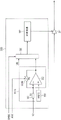
Fig. 1 is a block diagram for explaining a motor system according to a comparative example.
Fig. 2 is a diagram for explaining a sense current of the IGBT.
Fig. 3 is a block diagram for explaining an electric motor system according to a first example.
Fig. 4 is a block diagram illustrating electronics that are part of the electric motor system of fig. 3.
Fig. 5 is a block diagram for explaining the driver IC in fig. 4.
Fig. 6 is a circuit diagram for explaining the current mirror circuit in fig. 5.
Fig. 7 is a block diagram for explaining the configuration of the driving capability control circuit in fig. 5.
Fig. 8 is a timing chart for explaining control of the control driving capability control circuit in fig. 5.
Fig. 9 is a block diagram for explaining an IGBT and a driver IC according to a second example.
Fig. 10 is a diagram for explaining the IGBT in fig. 9.
Fig. 11 is a block diagram for explaining a driver IC and a control circuit according to a third example.
Fig. 12 is a block diagram for explaining the driving capability control circuit in fig. 11.
Fig. 13 is a block diagram for explaining the driving capability control circuit in fig. 11.
Fig. 14 is a block diagram for explaining a semiconductor integrated circuit device according to the embodiment.
Detailed Description
Examples of embodiments, examples, and modifications are described below with reference to the accompanying drawings. In the following description, like reference numerals are used to denote like parts and redundant description may be omitted.
First, a prior art (hereinafter referred to as a comparative example) before the present disclosure, which was studied by the inventors, is described.
Fig. 1 is a block diagram showing an electric motor system according to a comparative example. Fig. 2 is a diagram for explaining a sense current of the IGBT. The electric motor system 1R includes a three-phase motor 10, a reverse circuit 20, a driver IC30R, and a control circuit 40R. The three-phase motor 10 includes three transformers (coils) 11. The transformers may be two in that if two phases of current can be detected, a calculation of the current for each phase can be made. The inverter circuit 20 has a three-phase bridge configuration through six power semiconductor devices 21. As shown in fig. 2, the power semiconductor device 21 includes an IGBT22, and the IGBT22 is a switching transistor. The IGBT22 includes a gate terminal G, a collector terminal C, an emitter terminal E allowing a drive current to flow, and a sense terminal SE allowing a sense current to flow. The driver IC30R drives the power semiconductor device 21, and the control circuit 40R controls the driver IC 30R.
In order to drive the motor, in the inverter circuit using the IGBT22, it is necessary to control a drive signal (PWM signal) that drives the IGBT22 while monitoring a drive current. Regarding the monitoring of the current, the following two points are performed:
(1) the motor drive current of each phase is monitored, for example, by using an a/D converter such as the transformer 11 and the control circuit 40R, and the motor drive current of each phase is used to detect a normal current for controlling the drive motor.
(2) The sense current is monitored, for example, by employing, for example, a voltage comparison circuit and an a/D converter in the driver IC30R, and is mainly used to detect an overcurrent to cut off the drive signal when an abnormal current occurs.
The drive current of the IGBT22 is an emitter current (Ie), and the sense current is referred to as a current mirror current (I γ) because the sense current is a current of a current mirror circuit in the IGBT 22. The ratio (Ie/I γ) of the emitter current (Ie) to the current mirror current (I γ) is referred to as the current mirror ratio. The current mirror ratio is selected to be about 1000 to about 10000. Assuming that the normal drive current of the motor is about 400A, the rated current is about 1600A. Therefore, in the case of determining an abnormality exceeding the rated current value using the sense current, the current detection voltage (Vab) in the abnormal current detection is as follows, assuming that the current mirror ratio is 4000 and the resistance (Rab) for current detection is 5 Ω.
Vab=(1600A/4000)x 5Ω=2V
Meanwhile, the current detection voltage (Vn) in the normal operation is as follows:
Vn=(400/4000)x 5Ω=0.5V
further, in the low speed range of the motor, the dynamic range is small because the driving current is small.
At the start of rotation of the motor or in a low speed range of the motor, it is desirable to increase not only the PWM signal as the drive signal but also the current of the drive signal in order to improve the drive capability. However, in the current detection described in (1), the output voltage of the transformer may undergo a/D conversion in the control circuit 40R, and the drive control is adjusted based on the a/D conversion result, so that a cycle time is required and thus high-speed processing is difficult. Further, in the case of performing control by sensing a current as described in (2), it is difficult to obtain a sufficient gain due to the adoption of a loop suitable for abnormal current detection.
< example >
Fig. 14 is a block diagram for explaining a semiconductor integrated circuit device according to the embodiment. The semiconductor integrated circuit device 30 includes a drive circuit 31 and a drive capability control circuit 34, the drive circuit 31 driving the power semiconductor device 21, the drive capability control circuit 34 controlling the drive capability of the drive circuit 31. The drive circuit 31 stops driving the power semiconductor device 21 based on the abnormal current detected from the sense current of the power semiconductor device 21. The driving capability control circuit 34 controls the driving capability of the driving circuit 31 based on the normal current detected from the sense current of the power semiconductor device 21.
The driving capability of the power semiconductor device is improved, making it possible to drive a motor having a high torque, for example.
First example
(electric Motor System)
Fig. 3 is a block diagram showing an electric motor system according to a first example. The electric motor system 1 of fig. 3 includes a three-phase motor 10, an inverter circuit 20 employing six power semiconductor devices, six driver ICs 30, a control circuit 40, and a DC power supply 50. The portion composed of the inverter circuit 20, the six driver ICs 30 and the control circuit 40 is referred to as an electronic device 2. When driving a car or the like, the inverter circuit 20 controls the switching of the switching transistor 22 in the inverter circuit 20 to allow current to flow from the voltage of the DC power supply (DC)50 to the respective phases of the three-phase motor 10, so that the speed of the car or the like is changed by the switching frequency. When a vehicle or the like is braked, the inverter circuit 20 controls the on and off of the switching transistor 22 in synchronization with the voltage generated by each phase of the three-phase motor 10 to perform a so-called rectifying operation of obtaining a DC voltage, so that regeneration is performed.
The three-phase motor 10 includes a permanent magnet as a rotor and a coil as an armature. The three-phase armature windings (U-phase, V-phase and W-phase) are spaced 120 degrees apart in the delta connection. The current always flows through the three windings of the U-, V-and W-phases. The three-phase motor 10 includes a current detector 11 such as a transformer and an angular velocity and position detector 12.
The inverter circuit 20 forms a bridge circuit of U-, V-, and W-phases by a power semiconductor device. The U-phase bridge circuit is coupled to the three-phase motor 10 at a coupling point between the power semiconductor device 21U and the power semiconductor device 21X. The V-phase bridge circuit is coupled to the three-phase motor 10 at a coupling point between the power semiconductor device 21V and the power semiconductor device 21Y. The W-phase bridge circuit is coupled to the three-phase motor 10 at a coupling point between the power semiconductor device 21W and the power semiconductor device 21Z. Since the power semiconductor devices 21U, 21V, 21W, 21X, 21Y, and 21Z are the same in configuration, they may be collectively referred to as the power semiconductor device 21. The power semiconductor device 21 is formed of a semiconductor chip including a switching semiconductor (hereinafter abbreviated as IGBT)22 configured by an IGBT and a temperature detection diode D1, and a semiconductor chip including a flywheel diode D2, the flywheel diode D2 being coupled in parallel between an emitter and a collector of the IGBT 22. Freewheeling diode D2 is coupled so that current can flow in the opposite direction to the current flowing through the IGBT. Preferably, the semiconductor chip on which the IGBT22 and the temperature detection diode D1 are formed and the semiconductor chip on which the flywheel diode D2 is formed are sealed in the same package. The freewheeling diode D2 may be formed on the same semiconductor chip as the IGBT22 and the temperature sensing diode D1.
The driver IC30, as a first semiconductor integrated circuit device, includes a drive circuit (driver) 31 that generates a signal to drive the gate of the IGBT22, a current detection circuit (current detection) 32, a protection detection circuit (protection detection) 33, and a drive capability control circuit (drive capability controller) 34 on one semiconductor substrate. The control circuit 40 is a second semiconductor integrated circuit device including a CPU 41, a PWM circuit (PWM)42, and an I/O interface (I/O IF)43 on one semiconductor substrate and formed by, for example, a microcomputer unit (MCU). The CPU 41 operates according to a program stored in a nonvolatile memory, such as a flash memory (not shown), which is electrically erasable and rewritable.
(driver IC, control circuit)
Fig. 4 is a block diagram illustrating electronics that are part of the electric motor system in fig. 3. The driver IC30 includes a drive circuit 31, a current detection circuit 32, a protection detection circuit 33, an isolator 34, and a drive capability control circuit 35. The current detection circuit 32 includes a current amplification circuit (current AMP)32-1 that detects an abnormal current and a current amplification circuit (current AMP)32-2 that detects a normal current. The current amplification circuit (current AMP)32-1 converts the sense current into a voltage (V1), and the protection detection circuit 33 detects an abnormal current based on the voltage. The detection result is sent to the drive circuit 31 to turn off the drive signal of the IGBT 22. Also, the detection result is sent to the CPU 41 through the isolator 34 and the I/O interface 44 of the control circuit 40. The current amplification circuit (current AMP)32-2 converts the normal current into a voltage (V2). This voltage is sent to the driving capability control circuit 35, so that the driving capability control circuit 35 controls the driving capability of the driving circuit 31. The isolator 34 transmits signals required to be transmitted between the driver IC30 and the control circuit 40 through magnetic coupling. The isolator 34 is formed by insulating the on-chip transformer formed by the wire winding with an interlayer film.
Fig. 5 is a block diagram for illustrating the driver IC in fig. 4. The current detection circuit 32 is formed of a current mirror circuit (current mirror) 321, and resistors 322 and 323 are coupled to terminals T1 and T2, respectively. The current mirror circuit 321 divides the current (I γ) into an abnormal current (I γ 1) and a normal current (I γ 2), which flows from the current sense terminal NE of the IGBT22 to the current mirror circuit 32 via the terminal T3. A current mirror ratio and a detection resistance suitable for normal current detection and abnormal current detection are set. Assuming that the resistance value of the resistor 322 for detecting an abnormal current is RS1, the resistance value of the resistor 323 for detecting a normal current is RS2, the voltage for detecting an abnormal current is V1, and the voltage for detecting a normal current is V2, then:
V1=Iγ1x RS1
V2=Iγ2x RS2
the protection detection circuit 33 includes a comparator 331, a reference voltage generation circuit 332, and a filter 333. The comparator 331 compares the abnormal current detection voltage (V1) input to its non-inverting input terminal via the filter (filter) 333 with the reference voltage (VREF1) of the reference voltage generation circuit 332 input to its inverting input terminal, and, when V1 is greater than VREF1, detects an abnormal current and outputs an abnormal current signal (ABN).
The drive circuit 31 includes a driver 311, an and gate 312, and a state holding circuit 313. The state holding circuit 313 holds the abnormal current signal (ABN) detected by the protection monitoring circuit 33. When the abnormal current signal (ABN) indicates the occurrence of an abnormality, the state holding circuit 313 sets the output of 312 to low to cut off the drive signal (DRV) input from the terminal T4. The state holding circuit 313 allows the and gate 312 to pass the driving signal (DRV) therethrough in the case where the abnormal current signal (ABN) indicates that no abnormality has occurred. Based on the voltage control or the current control of the driving capability control circuit 35, the driver 311 issues a driving signal (DRV) to the gate terminal G of the IGBT22 via the terminal T5. The abnormal current signal (ABN) is sent to the control circuit 40 via the terminal T6.
Fig. 6 is a circuit diagram for explaining the current mirror circuit in fig. 5. The current mirror circuit 321 includes an operational amplifier 324, a filter capacitance 325, transistors Q1, Q2, and Q3, and resistors 322, 323, 326, 327, 328, 329, and 32A. When the receiving buffer circuit is configured by the input operational amplifier 324 to which the current mirror current (I γ) of the transistor Q1 and the IGBT22 flows, the same voltage as the reference voltage of the transistor Q1 is input to the other transistors Q2 and Q3, and the current amplification in the transistors Q2 and Q3 is designed to obtain a desired value, respectively, for example, the current of the transistor Q2 may be set to I γ x 1 and the current of the transistor Q3 may be set to I γ x 10.
Fig. 7 is a block diagram for explaining the configuration of the driving capability control circuit in fig. 5. The driving capability control circuit 35 includes an amplification circuit 351, a reference voltage generation circuit 355, a switching circuit 356, and a voltage or current control circuit (V/I controller) 357. The amplification circuit 351 is an inverting differential amplification circuit formed of an operational amplifier 352 and resistors 353 and 354, and amplifies a voltage (V3) obtained by multiplying a difference between a reference voltage (VREF2) of the reference voltage generation circuit 355 and a normal current detection voltage (V2) by a ratio of a resistance value (R2) of the resistor 353 and a resistance value (R1) of the resistor 354.
V3=(VREF2-V2)x R2/R1
When V2 was small, V3 was large. When V2 is large, V3 is small.
The switching circuit 356 switches between a basic setting Voltage (VB) and a voltage (V3) to supply the voltage to the voltage or current control circuit 357 based on a driving capability control signal (DRBC) input from the control circuit 40 via a terminal T7.
The voltage or current control circuit 357 controls the voltage or current of the driver 311 to control the output voltage or output current of the driver 311. The voltage (V3) is higher than the basic setting Voltage (VB), and when the basic setting Voltage (VB) is switched to the voltage (V3), the output voltage or output current of the driver 311 increases.
Fig. 8 is a timing chart for explaining control of the control driving capability control circuit in fig. 5. In a low speed (high torque) range of the motor, one power source cycle is set longer and the duty (duty) of the PWM signal is set larger than in a medium/high speed range. Also, in the low speed range, the drive capability control signal (DRBC) input from the terminal T7 causes switching to the voltage (V3) so as to set the drive capability of the driver 311 higher. In the medium/high speed range, the driving capability control signal (DRBC) causes switching to the basic setting Voltage (VB).
According to this example, in order to improve the driving capability, not only the PWM signal as the driving signal but also the current of the driving signal may be increased at the start of the motor rotation or during the rotation at a low speed. In addition, current detection is performed with the sense current without using a transformer. Therefore, a cycle time is not required in which the drive control is adjusted by the transformer output voltage subjected to the a/D conversion in the control circuit 40 and based on the a/D conversion result. Therefore, high-speed processing is easily achieved. Further, a loop suitable for abnormal current detection and a loop suitable for normal current detection are employed at the same time. Therefore, a sufficient gain can be obtained.
Second example
Fig. 9 is a block diagram for explaining an electronic device according to a second example. The electronic device according to the second example includes two current mirrors in one IGBT, but omits a current mirror circuit in a driver IC according to the first example. The other configurations are the same as in the first example.
The IGBT22 in the first example is formed of thousands to tens of thousands of cells (cells) having the same configuration. A part of these cells is used as a cell for detecting a sense current (abnormal current), a region formed by the cell for detecting the sense current is referred to as an "abnormal current detection region", and a region formed by other cells is referred to as a "main region". The ratio (Nm/Ns) of the number of cells in the main area (Nm: integer) to the number of cells in the abnormal current detection area (Ns: integer) is set to be several thousands. The IGBT 22A in the second example further includes cells for detecting a sense current (normal current), and a region formed by those cells is referred to as a normal current detection region. Assuming that the number of cells in the normal current detection region is Nns (integer), Nns/Ns may be set to 10, for example.
As shown in fig. 10, the collector terminal of the IGBT 22A is common to the main region, the abnormal current detection region, and the normal current detection region, whereas the emitter terminals are divided into a main emitter terminal E (hereinafter referred to as main terminal), an emitter terminal SE (hereinafter referred to as sense terminal) for normal current detection, and an emitter terminal NSE (hereinafter referred to as normal sense terminal) for normal current detection. The gate terminal G for driving each region is common.
The current mirror current (I γ 1) from the sense terminal SE generates an abnormal current detection voltage (V1) through the resistor 322 to detect an abnormal current coupled to the T1 terminal. The current mirror circuit of the IGBT 22A and the resistor 322 for detecting an abnormal current form an abnormal current detection circuit. The current mirror current (I γ 2) from the normal sense terminal NSE generates a normal current detection voltage (V2) through the resistor 323 to detect a normal current coupled to the T2 terminal. The current mirror circuit of the IGBT 22A and the resistor 323 for detecting a normal current form a normal current detection circuit.
According to the present example, since no current mirror circuit is required in the driver IC, the driver IC can have a simpler configuration than the first example, thereby reducing the chip area.
Third example
Fig. 11 is a block diagram for explaining an electronic device according to a third example. The electronic device according to the third example further includes an a/D converter in the driver IC of the first example and may perform feedback to the driving-capability control circuit. The other configurations are the same as the first example.
The driver IC 30B includes an a/C converter (ADC)36 that informs the control circuit 40B of a normal current detection voltage (Vn) and an abnormal current detection voltage (Va) as outputs of the current detection circuit 32 (the current amplification circuits 32-1 and 32-2). The output of the a/D converter 36 is sent to the control circuit 40B via the isolator 34B and the terminal T9.
Fig. 12 is a block diagram for explaining the driving capability control circuit in fig. 11. The driving capability control circuit in the third example has a function of causing the resistance value of the loop resistor in the amplification circuit to be adjusted, and the other configurations are the same as in the first example. The control circuit 40B generates a control signal (AGC) based on the voltage (Vn) obtained by the a/D converter 36. The resistor 354B of the amplification circuit 351B of the driving capability control circuit 35B is a variable resistor whose resistance value is adjustable based on a control signal (AGC) input from the terminal T8. Since a function of making the feedback gain of the normal current detection voltage (Vn) adjustable (a function of making the loop resistor 354B of the amplifying circuit 351B adjustable) is provided, it becomes possible to control the driving capability with high accuracy by adjusting the gain in accordance with the change of the resistance value (RS2) of the resistor 323 for detecting the normal current.
< modified example >
Fig. 13 is a block diagram for explaining the driving capability control circuit in fig. 11. The driving capability control circuit in the present example has a function of allowing the reference voltage (VREF2) in the first example to be adjusted, and the other configuration is the same as that in the first example. The control circuit 40B generates a control signal (RVC) based on the voltage (Vn) obtained by the a/D converter 36. The reference voltage (VREF2) of the reference voltage generation circuit 355C of the driving capability control circuit 35C is variable and can be adjusted based on the control signal (RVC) input from the terminal T8. Since a function of making the feedback gain of the normal current detection voltage (Vn) adjustable (a function of making the reference voltage (VREF2) of the reference voltage generation circuit 335C adjustable) is provided, it becomes possible to control the driving capability with high accuracy by adjusting the gain in accordance with the change of the resistance value (RS2) of the resistor 323 for detecting the normal current.
The invention made by the inventors has been described above specifically based on the embodiments, examples, and modified examples. It should be noted, however, that the present invention is not limited thereto, but can be modified in various ways.
Claims (20)
1. A semiconductor integrated circuit device comprising:
a drive circuit configured to drive the power semiconductor device;
a driving capability control circuit configured to control a driving capability of the driving circuit; and
a current detection circuit configured to receive a sense current of the power semiconductor device and output a first control signal to the driving circuit and a second control signal to the driving capability control circuit, the second control signal being separate from the first control signal,
wherein the drive circuit is further configured to receive the first control signal and to stop driving the power semiconductor device based on the first control signal, an
Wherein the drive capability control circuit is further configured to receive the second control signal and control the drive capability of the drive circuit based on the second control signal.
2. The semiconductor integrated circuit device according to claim 1, wherein the current detection circuit comprises:
a first current detection circuit configured to receive the sense current and output an abnormal current detection voltage as the first control signal based on the sense current of the power semiconductor device, an
A second current detection circuit configured to receive the sense current and output a normal current detection voltage as the second control signal based on the sense current of the power semiconductor device.
3. The semiconductor integrated circuit device according to claim 2, wherein the drive-capability control circuit comprises:
a voltage generating circuit that generates a voltage based on the normal current detection voltage, an
A control circuit that controls a voltage or a current of the driving circuit based on the generated voltage.
4. The semiconductor integrated circuit device according to claim 3,
wherein the voltage generation circuit includes an amplification circuit having an operational amplifier and a loop resistor, and a circuit generating a reference voltage, and
wherein the resistance value of the loop resistor or the reference voltage may be changed based on a third control signal.
5. The semiconductor integrated circuit device according to claim 4, further comprising:
an A/D conversion circuit converting the normal current detection voltage;
a terminal that outputs an output of the a/D conversion circuit; and
a terminal to which the third control signal generated based on the output of the a/D conversion circuit is input.
6. The semiconductor integrated circuit device according to claim 1, further comprising:
a first terminal to be coupled to a terminal outputting the sense current from which an abnormal current of the power semiconductor device is detected, an
A second terminal to be coupled to a terminal outputting the sense current from which a normal current is detected.
7. The semiconductor integrated circuit device according to claim 6,
wherein a resistor for detecting the abnormal current of the power semiconductor device is coupled to the outside so that the first terminal is configured to receive an abnormal current detection voltage, and
wherein a resistor for detecting the normal current of the power semiconductor device is coupled to the outside such that the second terminal is configured to receive a normal current detection voltage.
8. The semiconductor integrated circuit device according to claim 7,
wherein the driving capability control circuit includes:
a circuit that generates a voltage based on the normal current detection voltage; and
a control circuit that controls a voltage or a current of the driving circuit based on the generated voltage.
9. The semiconductor integrated circuit device according to claim 1, wherein the current detection circuit simultaneously outputs the first control signal and the second control signal.
10. The semiconductor integrated circuit device according to claim 1, wherein the drive-capability control circuit is further configured to change the drive capability of the drive circuit based on the second control signal, while the drive circuit drives the power semiconductor device based on the first control signal.
11. A semiconductor integrated circuit device comprising:
a drive circuit that drives the power semiconductor device; and
a drive capability control circuit that controls a drive capability of the drive circuit, wherein the drive circuit stops driving the power semiconductor device based on an abnormal current detected from a sense current of the power semiconductor device, and wherein the drive capability control circuit controls the drive capability of the drive circuit based on a normal current detected from the sense current of the power semiconductor device;
a first current detection circuit that outputs an abnormal current detection voltage based on the sense current of the power semiconductor device; and
a second current detection circuit outputting a normal current detection voltage based on the sense current of the power semiconductor device,
wherein the first current detection circuit and the second current detection circuit are respectively formed by current mirror circuits, an
Wherein a first resistor and a second resistor are provided, the first resistor being coupled to a first terminal of the current mirror circuit for detecting the abnormal current to the external power semiconductor device, and the second resistor being coupled to a second terminal of the current mirror circuit for detecting the normal current to the external power semiconductor device.
12. An electronic device, comprising:
a power semiconductor device;
a first semiconductor integrated circuit device; and
a second semiconductor integrated circuit device having a plurality of semiconductor chips,
wherein the first semiconductor integrated circuit device includes:
a drive circuit configured to drive the power semiconductor device;
a driving capability control circuit configured to control a driving capability of the driving circuit; and
a current detection circuit configured to receive a sense current of the power semiconductor device and output a first control signal to the driving circuit and a second control signal to the driving capability control circuit, the second control signal being separate from the first control signal,
wherein the drive circuit is further configured to receive the first control signal and to stop driving the power semiconductor device based on the first control signal, an
Wherein the drive capability control circuit is further configured to receive the second control signal and control the drive capability of the drive circuit based on the second control signal.
13. The electronic device as set forth in claim 12,
wherein the power semiconductor device includes:
a first terminal for supplying current for driving a load, an
A second terminal providing a current for monitoring the drive current, an
Wherein the current detection circuit of the first semiconductor integrated circuit includes:
a first current detection circuit configured to receive the sense current and output an abnormal current detection voltage as the first control signal based on the current from the second terminal, an
A second current detection circuit configured to receive the sense current and output a normal current detection voltage as the second control signal based on the current from the second terminal.
14. The electronic device as set forth in claim 13,
wherein the first semiconductor integrated circuit device includes:
a fourth terminal which couples a resistor for detecting an abnormal current of the power semiconductor device to the outside, an
A fifth terminal coupling a resistor for detecting a normal current of the power semiconductor device to the outside;
wherein the first current detection circuit and the second current detection circuit are respectively formed by current mirror circuits.
15. The electronic device as set forth in claim 13,
wherein the drive capability control circuit of the first semiconductor integrated circuit device includes:
a voltage generation circuit that generates a voltage based on the normal current detection voltage; and
a control circuit that controls a voltage or a current of the driving circuit based on the generated voltage.
16. The electronic device as set forth in claim 15,
wherein the voltage generation circuit includes an amplification circuit having an operational amplifier and a loop resistor, and a circuit generating a reference voltage, and
wherein the resistance value of the loop resistor or the reference voltage may be changed based on a third control signal.
17. The electronic device as set forth in claim 16,
wherein the first semiconductor integrated circuit further includes an A/D conversion circuit that converts the normal current detection voltage, and
wherein the second semiconductor integrated circuit device includes a CPU that generates the third control signal based on an output of the a/D conversion circuit.
18. The electronic device as set forth in claim 13,
wherein the power semiconductor device includes:
a first terminal for supplying a current for driving a load, an
A second terminal providing a current for monitoring the drive current, an
A third terminal supplying a current for monitoring the driving current, an
Wherein the first semiconductor integrated circuit device includes:
a fourth terminal to be coupled to the second terminal, an
A fifth terminal to be coupled to the third terminal.
19. The electronic device of claim 18, further comprising:
a resistor coupled to the third terminal for detecting an abnormal current of the power semiconductor device; and
a resistor coupled to the fourth terminal for detecting a normal current of the power semiconductor device;
wherein the third terminal is configured to receive the abnormal current detection voltage, and
wherein the fourth terminal is configured to receive the normal current detection voltage.
20. The electronic device as set forth in claim 19,
wherein the driving capability control circuit includes:
a circuit for generating a voltage based on the normal current detection voltage, an
A control circuit that controls a voltage or a current of the driving circuit based on the generated voltage.
Applications Claiming Priority (2)
| Application Number | Priority Date | Filing Date | Title |
|---|---|---|---|
| JP2015172625A JP6549451B2 (en) | 2015-09-02 | 2015-09-02 | Semiconductor integrated circuit device and electronic device |
| JP2015-172625 | 2015-09-02 |
Publications (2)
| Publication Number | Publication Date |
|---|---|
| CN106487264A CN106487264A (en) | 2017-03-08 |
| CN106487264B true CN106487264B (en) | 2020-08-28 |
Family
ID=58103744
Family Applications (1)
| Application Number | Title | Priority Date | Filing Date |
|---|---|---|---|
| CN201610670696.8A Active CN106487264B (en) | 2015-09-02 | 2016-08-15 | Semiconductor integrated circuit device for driving power semiconductor device and electronic device |
Country Status (3)
| Country | Link |
|---|---|
| US (2) | US9835658B2 (en) |
| JP (1) | JP6549451B2 (en) |
| CN (1) | CN106487264B (en) |
Families Citing this family (6)
| Publication number | Priority date | Publication date | Assignee | Title |
|---|---|---|---|---|
| JP2018093684A (en) * | 2016-12-07 | 2018-06-14 | ルネサスエレクトロニクス株式会社 | Semiconductor device and power conversion device |
| WO2019049698A1 (en) * | 2017-09-08 | 2019-03-14 | パナソニックIpマネジメント株式会社 | Power conversion circuit and power conversion device |
| DE102019119973B3 (en) * | 2019-07-24 | 2021-01-21 | Infineon Technologies Ag | INTELLIGENT ELECTRONIC SWITCH |
| KR20210015261A (en) * | 2019-08-01 | 2021-02-10 | 현대자동차주식회사 | Overcurrent detection reference compensation system of switching element for inverter and overcurrent detection system using the same |
| CN111653852B (en) * | 2020-05-19 | 2021-06-11 | 南京理工大学 | On-chip transformer-based transmission zero-point adjustable filter |
| DE102020123149A1 (en) | 2020-09-04 | 2022-03-10 | Infineon Technologies Ag | CONTROL CIRCUIT FOR ELECTRONIC SWITCH |
Citations (3)
| Publication number | Priority date | Publication date | Assignee | Title |
|---|---|---|---|---|
| JPS6395728A (en) * | 1986-10-13 | 1988-04-26 | Fuji Electric Co Ltd | Overcurrent protection circuit for igbt |
| US5710508A (en) * | 1995-05-16 | 1998-01-20 | Fuji Electric Co., Ltd. | Semiconductor apparatus |
| CN104852714A (en) * | 2014-02-19 | 2015-08-19 | 株式会社电装 | Gate driver |
Family Cites Families (16)
| Publication number | Priority date | Publication date | Assignee | Title |
|---|---|---|---|---|
| US5061863A (en) * | 1989-05-16 | 1991-10-29 | Kabushiki Kaisha Toyoda Jidoshokki Seisakusho | Transistor provided with a current detecting function |
| JP2800277B2 (en) * | 1989-06-26 | 1998-09-21 | 株式会社豊田自動織機製作所 | Semiconductor element drive circuit |
| JP2000323974A (en) * | 1999-05-12 | 2000-11-24 | Fuji Electric Co Ltd | Short-circuit protecting circuit for semiconductor element |
| US6717785B2 (en) * | 2000-03-31 | 2004-04-06 | Denso Corporation | Semiconductor switching element driving circuit |
| JP2006187101A (en) * | 2004-12-27 | 2006-07-13 | Nissan Motor Co Ltd | Method of driving voltage driver element |
| JP4619812B2 (en) * | 2005-02-16 | 2011-01-26 | 株式会社東芝 | Gate drive circuit |
| EP1755221B1 (en) * | 2005-08-17 | 2009-12-09 | Infineon Technologies AG | Method and driver circuit for controlling a power MOS transistor |
| JP2007228447A (en) * | 2006-02-27 | 2007-09-06 | Hitachi Ltd | Gate drive circuit for switching element |
| JP5443946B2 (en) | 2009-11-02 | 2014-03-19 | 株式会社東芝 | Inverter device |
| JP5678498B2 (en) * | 2010-07-15 | 2015-03-04 | 富士電機株式会社 | Gate drive circuit for power semiconductor device |
| US8633755B2 (en) * | 2010-11-22 | 2014-01-21 | Denso Corporation | Load driver with constant current variable structure |
| JP5783121B2 (en) * | 2012-04-09 | 2015-09-24 | 株式会社デンソー | Driving device for driven switching element |
| JP5790880B2 (en) * | 2012-06-22 | 2015-10-07 | 富士電機株式会社 | Overcurrent detection device and intelligent power module using the same |
| US8703091B2 (en) * | 2012-07-31 | 2014-04-22 | Uht Unitech Co., Ltd. | High modulus graphite fiber and manufacturing method thereof |
| CN104871417B (en) * | 2012-12-21 | 2018-03-06 | 三菱电机株式会社 | Switch element driver circuit, power model and automobile |
| JP6065597B2 (en) * | 2013-01-16 | 2017-01-25 | 富士電機株式会社 | Power converter |
-
2015
- 2015-09-02 JP JP2015172625A patent/JP6549451B2/en active Active
-
2016
- 2016-07-22 US US15/216,859 patent/US9835658B2/en active Active
- 2016-08-15 CN CN201610670696.8A patent/CN106487264B/en active Active
-
2017
- 2017-10-30 US US15/797,757 patent/US10324114B2/en active Active
Patent Citations (3)
| Publication number | Priority date | Publication date | Assignee | Title |
|---|---|---|---|---|
| JPS6395728A (en) * | 1986-10-13 | 1988-04-26 | Fuji Electric Co Ltd | Overcurrent protection circuit for igbt |
| US5710508A (en) * | 1995-05-16 | 1998-01-20 | Fuji Electric Co., Ltd. | Semiconductor apparatus |
| CN104852714A (en) * | 2014-02-19 | 2015-08-19 | 株式会社电装 | Gate driver |
Also Published As
| Publication number | Publication date |
|---|---|
| US9835658B2 (en) | 2017-12-05 |
| US10324114B2 (en) | 2019-06-18 |
| JP6549451B2 (en) | 2019-07-24 |
| CN106487264A (en) | 2017-03-08 |
| US20170063367A1 (en) | 2017-03-02 |
| JP2017050984A (en) | 2017-03-09 |
| US20180067150A1 (en) | 2018-03-08 |
Similar Documents
| Publication | Publication Date | Title |
|---|---|---|
| CN106487264B (en) | Semiconductor integrated circuit device for driving power semiconductor device and electronic device | |
| KR102649093B1 (en) | Power conversion device and semiconductor device | |
| CN106953503B (en) | Semiconductor integrated circuit device and electronic device | |
| US10291110B2 (en) | Driving circuit for switching element and power conversion system | |
| JP6183282B2 (en) | Vehicle generator | |
| US10050560B1 (en) | Inverter circuit with current detection circuitry | |
| US20100013422A1 (en) | Motor driving apparatus and control method thereof | |
| US10658947B2 (en) | Semiconductor device, power module, and control method of power conversion device | |
| JP2009303338A (en) | Motor driving device and control method of motor driving device | |
| JP5716158B2 (en) | Motor current detection IC and current detector or motor control device using the same | |
| JP2015171200A (en) | Semiconductor device, motor using the same, and air conditioner | |
| WO2017187813A1 (en) | Current detection device | |
| KR20160108214A (en) | Electronic device | |
| JP2015033149A (en) | Drive unit of semiconductor element and power conversion device using the same | |
| JP5477159B2 (en) | Motor current detection IC and current detector or motor control device using the same | |
| US10720871B2 (en) | Driving circuit and motor | |
| JP2019146354A (en) | Gate drive circuit for inverter and on-vehicle electronic control device | |
| JPWO2016174756A1 (en) | Protection circuit and protection circuit system | |
| JP2016093074A (en) | Inverter system | |
| JP2019140845A (en) | Motor drive circuit, fan motor, drive control circuit and motor system |
Legal Events
| Date | Code | Title | Description |
|---|---|---|---|
| C06 | Publication | ||
| PB01 | Publication | ||
| SE01 | Entry into force of request for substantive examination | ||
| SE01 | Entry into force of request for substantive examination | ||
| GR01 | Patent grant | ||
| GR01 | Patent grant |