CN106248224B - Light detection device and light detection system - Google Patents
Light detection device and light detection system Download PDFInfo
- Publication number
- CN106248224B CN106248224B CN201610286166.3A CN201610286166A CN106248224B CN 106248224 B CN106248224 B CN 106248224B CN 201610286166 A CN201610286166 A CN 201610286166A CN 106248224 B CN106248224 B CN 106248224B
- Authority
- CN
- China
- Prior art keywords
- light
- detector
- refractive index
- detectors
- index layer
- Prior art date
- Legal status (The legal status is an assumption and is not a legal conclusion. Google has not performed a legal analysis and makes no representation as to the accuracy of the status listed.)
- Active
Links
- 238000001514 detection method Methods 0.000 title claims abstract description 92
- 238000010168 coupling process Methods 0.000 claims abstract description 55
- 238000005859 coupling reaction Methods 0.000 claims abstract description 55
- 230000008878 coupling Effects 0.000 claims abstract description 54
- 238000009826 distribution Methods 0.000 claims description 51
- 230000003287 optical effect Effects 0.000 claims description 49
- 239000010410 layer Substances 0.000 description 135
- 238000010586 diagram Methods 0.000 description 58
- 239000000126 substance Substances 0.000 description 25
- 238000000034 method Methods 0.000 description 15
- 230000001902 propagating effect Effects 0.000 description 15
- 230000008859 change Effects 0.000 description 14
- 239000011295 pitch Substances 0.000 description 14
- 238000004458 analytical method Methods 0.000 description 12
- 238000012545 processing Methods 0.000 description 11
- 238000000342 Monte Carlo simulation Methods 0.000 description 10
- 210000003128 head Anatomy 0.000 description 10
- 230000010355 oscillation Effects 0.000 description 10
- 230000005855 radiation Effects 0.000 description 7
- 239000007787 solid Substances 0.000 description 7
- 238000006073 displacement reaction Methods 0.000 description 6
- 238000005086 pumping Methods 0.000 description 6
- 239000000758 substrate Substances 0.000 description 6
- 238000004364 calculation method Methods 0.000 description 5
- 230000002123 temporal effect Effects 0.000 description 5
- 230000035559 beat frequency Effects 0.000 description 4
- 230000005540 biological transmission Effects 0.000 description 4
- 210000000887 face Anatomy 0.000 description 4
- 239000002184 metal Substances 0.000 description 4
- 230000002238 attenuated effect Effects 0.000 description 3
- 230000015556 catabolic process Effects 0.000 description 3
- 230000001427 coherent effect Effects 0.000 description 3
- 239000000470 constituent Substances 0.000 description 3
- 238000006731 degradation reaction Methods 0.000 description 3
- 230000000694 effects Effects 0.000 description 3
- 230000006870 function Effects 0.000 description 3
- 210000004761 scalp Anatomy 0.000 description 3
- 239000004065 semiconductor Substances 0.000 description 3
- 210000003625 skull Anatomy 0.000 description 3
- 238000012935 Averaging Methods 0.000 description 2
- 230000000903 blocking effect Effects 0.000 description 2
- 229910052681 coesite Inorganic materials 0.000 description 2
- 229910052906 cristobalite Inorganic materials 0.000 description 2
- 230000007423 decrease Effects 0.000 description 2
- 230000003247 decreasing effect Effects 0.000 description 2
- 238000003745 diagnosis Methods 0.000 description 2
- 239000006185 dispersion Substances 0.000 description 2
- 238000011156 evaluation Methods 0.000 description 2
- 230000014509 gene expression Effects 0.000 description 2
- 239000000463 material Substances 0.000 description 2
- 238000005259 measurement Methods 0.000 description 2
- 238000001320 near-infrared absorption spectroscopy Methods 0.000 description 2
- 230000000644 propagated effect Effects 0.000 description 2
- 238000011160 research Methods 0.000 description 2
- 239000000377 silicon dioxide Substances 0.000 description 2
- VYPSYNLAJGMNEJ-UHFFFAOYSA-N silicon dioxide Inorganic materials O=[Si]=O VYPSYNLAJGMNEJ-UHFFFAOYSA-N 0.000 description 2
- 238000004611 spectroscopical analysis Methods 0.000 description 2
- 229910052682 stishovite Inorganic materials 0.000 description 2
- PBCFLUZVCVVTBY-UHFFFAOYSA-N tantalum pentoxide Inorganic materials O=[Ta](=O)O[Ta](=O)=O PBCFLUZVCVVTBY-UHFFFAOYSA-N 0.000 description 2
- 229910052905 tridymite Inorganic materials 0.000 description 2
- 210000004885 white matter Anatomy 0.000 description 2
- 238000010521 absorption reaction Methods 0.000 description 1
- 239000000853 adhesive Substances 0.000 description 1
- 230000001070 adhesive effect Effects 0.000 description 1
- 230000002776 aggregation Effects 0.000 description 1
- 238000004220 aggregation Methods 0.000 description 1
- 238000013459 approach Methods 0.000 description 1
- 238000005452 bending Methods 0.000 description 1
- 230000008901 benefit Effects 0.000 description 1
- 239000002131 composite material Substances 0.000 description 1
- 238000007796 conventional method Methods 0.000 description 1
- 238000000354 decomposition reaction Methods 0.000 description 1
- 230000023077 detection of light stimulus Effects 0.000 description 1
- 230000006866 deterioration Effects 0.000 description 1
- 230000004069 differentiation Effects 0.000 description 1
- 230000001678 irradiating effect Effects 0.000 description 1
- 238000010030 laminating Methods 0.000 description 1
- 238000004519 manufacturing process Methods 0.000 description 1
- 239000002245 particle Substances 0.000 description 1
- 238000000059 patterning Methods 0.000 description 1
- 230000000737 periodic effect Effects 0.000 description 1
- 230000010287 polarization Effects 0.000 description 1
- 230000007261 regionalization Effects 0.000 description 1
- 229920006395 saturated elastomer Polymers 0.000 description 1
- 238000000926 separation method Methods 0.000 description 1
- 238000004904 shortening Methods 0.000 description 1
- 239000002344 surface layer Substances 0.000 description 1
Images


Classifications
-
- G—PHYSICS
- G01—MEASURING; TESTING
- G01J—MEASUREMENT OF INTENSITY, VELOCITY, SPECTRAL CONTENT, POLARISATION, PHASE OR PULSE CHARACTERISTICS OF INFRARED, VISIBLE OR ULTRAVIOLET LIGHT; COLORIMETRY; RADIATION PYROMETRY
- G01J9/00—Measuring optical phase difference; Determining degree of coherence; Measuring optical wavelength
- G01J9/02—Measuring optical phase difference; Determining degree of coherence; Measuring optical wavelength by interferometric methods
-
- G—PHYSICS
- G01—MEASURING; TESTING
- G01J—MEASUREMENT OF INTENSITY, VELOCITY, SPECTRAL CONTENT, POLARISATION, PHASE OR PULSE CHARACTERISTICS OF INFRARED, VISIBLE OR ULTRAVIOLET LIGHT; COLORIMETRY; RADIATION PYROMETRY
- G01J1/00—Photometry, e.g. photographic exposure meter
- G01J1/02—Details
- G01J1/04—Optical or mechanical part supplementary adjustable parts
- G01J1/0407—Optical elements not provided otherwise, e.g. manifolds, windows, holograms, gratings
- G01J1/0422—Optical elements not provided otherwise, e.g. manifolds, windows, holograms, gratings using light concentrators, collectors or condensers
-
- G—PHYSICS
- G01—MEASURING; TESTING
- G01J—MEASUREMENT OF INTENSITY, VELOCITY, SPECTRAL CONTENT, POLARISATION, PHASE OR PULSE CHARACTERISTICS OF INFRARED, VISIBLE OR ULTRAVIOLET LIGHT; COLORIMETRY; RADIATION PYROMETRY
- G01J1/00—Photometry, e.g. photographic exposure meter
- G01J1/02—Details
- G01J1/04—Optical or mechanical part supplementary adjustable parts
- G01J1/0407—Optical elements not provided otherwise, e.g. manifolds, windows, holograms, gratings
- G01J1/0448—Adjustable, e.g. focussing
-
- G—PHYSICS
- G02—OPTICS
- G02B—OPTICAL ELEMENTS, SYSTEMS OR APPARATUS
- G02B5/00—Optical elements other than lenses
- G02B5/18—Diffraction gratings
- G02B5/1809—Diffraction gratings with pitch less than or comparable to the wavelength
-
- G—PHYSICS
- G02—OPTICS
- G02B—OPTICAL ELEMENTS, SYSTEMS OR APPARATUS
- G02B5/00—Optical elements other than lenses
- G02B5/20—Filters
- G02B5/203—Filters having holographic or diffractive elements
-
- G—PHYSICS
- G02—OPTICS
- G02B—OPTICAL ELEMENTS, SYSTEMS OR APPARATUS
- G02B6/00—Light guides; Structural details of arrangements comprising light guides and other optical elements, e.g. couplings
-
- A—HUMAN NECESSITIES
- A61—MEDICAL OR VETERINARY SCIENCE; HYGIENE
- A61B—DIAGNOSIS; SURGERY; IDENTIFICATION
- A61B2562/00—Details of sensors; Constructional details of sensor housings or probes; Accessories for sensors
- A61B2562/02—Details of sensors specially adapted for in-vivo measurements
- A61B2562/0233—Special features of optical sensors or probes classified in A61B5/00
-
- A—HUMAN NECESSITIES
- A61—MEDICAL OR VETERINARY SCIENCE; HYGIENE
- A61B—DIAGNOSIS; SURGERY; IDENTIFICATION
- A61B2562/00—Details of sensors; Constructional details of sensor housings or probes; Accessories for sensors
- A61B2562/04—Arrangements of multiple sensors of the same type
- A61B2562/046—Arrangements of multiple sensors of the same type in a matrix array
-
- A—HUMAN NECESSITIES
- A61—MEDICAL OR VETERINARY SCIENCE; HYGIENE
- A61B—DIAGNOSIS; SURGERY; IDENTIFICATION
- A61B5/00—Measuring for diagnostic purposes; Identification of persons
- A61B5/0033—Features or image-related aspects of imaging apparatus classified in A61B5/00, e.g. for MRI, optical tomography or impedance tomography apparatus; arrangements of imaging apparatus in a room
- A61B5/004—Features or image-related aspects of imaging apparatus classified in A61B5/00, e.g. for MRI, optical tomography or impedance tomography apparatus; arrangements of imaging apparatus in a room adapted for image acquisition of a particular organ or body part
- A61B5/0042—Features or image-related aspects of imaging apparatus classified in A61B5/00, e.g. for MRI, optical tomography or impedance tomography apparatus; arrangements of imaging apparatus in a room adapted for image acquisition of a particular organ or body part for the brain
-
- A—HUMAN NECESSITIES
- A61—MEDICAL OR VETERINARY SCIENCE; HYGIENE
- A61B—DIAGNOSIS; SURGERY; IDENTIFICATION
- A61B5/00—Measuring for diagnostic purposes; Identification of persons
- A61B5/0059—Measuring for diagnostic purposes; Identification of persons using light, e.g. diagnosis by transillumination, diascopy, fluorescence
- A61B5/0062—Arrangements for scanning
- A61B5/0066—Optical coherence imaging
-
- G—PHYSICS
- G01—MEASURING; TESTING
- G01J—MEASUREMENT OF INTENSITY, VELOCITY, SPECTRAL CONTENT, POLARISATION, PHASE OR PULSE CHARACTERISTICS OF INFRARED, VISIBLE OR ULTRAVIOLET LIGHT; COLORIMETRY; RADIATION PYROMETRY
- G01J9/00—Measuring optical phase difference; Determining degree of coherence; Measuring optical wavelength
- G01J9/02—Measuring optical phase difference; Determining degree of coherence; Measuring optical wavelength by interferometric methods
- G01J2009/0211—Measuring optical phase difference; Determining degree of coherence; Measuring optical wavelength by interferometric methods for measuring coherence
-
- G—PHYSICS
- G02—OPTICS
- G02B—OPTICAL ELEMENTS, SYSTEMS OR APPARATUS
- G02B6/00—Light guides; Structural details of arrangements comprising light guides and other optical elements, e.g. couplings
- G02B6/24—Coupling light guides
- G02B6/26—Optical coupling means
- G02B6/34—Optical coupling means utilising prism or grating
Abstract
The present disclosure provides a light detection device and a light detection system, the light detection device including: a photodetector having a main surface, including at least 1 st detector and at least 1 nd 2 detector arranged along the main surface; a light coupling layer disposed on the photodetector, the light coupling layer including a1 st low refractive index layer, a1 st high refractive index layer disposed on the 1 st low refractive index layer and including a1 st grating, and a2 nd low refractive index layer disposed on the 1 st high refractive index layer, the 1 st high refractive index layer having a higher refractive index than the 1 st low refractive index layer and the 2 nd low refractive index layer; and a light shielding film, disposed on the light coupling layer, including at least 1 light transmitting region, and at least 1 light shielding region adjacent to the at least 1 light transmitting region, the at least 1 light transmitting region facing the at least 1 st detector, the at least 1 light shielding region facing the at least 1 nd 2 nd detector.
Description
Technical Field
The present disclosure relates to a light detection device, a light detection system, a light detection method, and the like.
Background
Light is an electromagnetic wave and is characterized by properties such as polarization and interference, in addition to wavelength and intensity. Among them, as a method for measuring the interference of light, for example, Michelson interferometer (Michelson interferometer) given in "optical principle" (eastern sea university press, p.482, M-born, etc.) can be cited.
Disclosure of Invention
A photodetection device according to an aspect of the present disclosure includes: a photodetector having a main surface, including at least 1 st detector and at least 1 nd 2 detector arranged along the main surface; a light coupling layer disposed on the photodetector, the light coupling layer including a1 st low refractive index layer, a1 st high refractive index layer disposed on the 1 st low refractive index layer and including a1 st grating, and a2 nd low refractive index layer disposed on the 1 st high refractive index layer, the 1 st high refractive index layer having a higher refractive index than the 1 st low refractive index layer and the 2 nd low refractive index layer; and a light shielding film, disposed on the light coupling layer, including at least 1 light transmitting region, and at least 1 light shielding region adjacent to the at least 1 light transmitting region, the at least 1 light transmitting region facing the at least 1 st detector, the at least 1 light shielding region facing the at least 1 nd 2 nd detector.
Drawings
Fig. 1A is a schematic diagram showing the light detection system and the subject according to embodiment 1.
Fig. 1B is an explanatory diagram showing a state of scattered light incident on one aperture of the photodetector.
Fig. 2A is a cross-sectional view of the photodetection device according to embodiment 1.
Fig. 2B is a plan view of the photodetection device according to embodiment 1 as viewed from the light incident side.
Fig. 3A is a cross-sectional view of the photodetection device according to embodiment 1.
Fig. 3B is a diagram showing a state in which 1 pulse of incident light passes through the optical coupling layer and is received by the detector in chronological order by electromagnetic analysis in embodiment 1.
Fig. 3C is a diagram showing a state in which 1 pulse of incident light passes through the optical coupling layer and is received by the detector in chronological order by electromagnetic analysis in embodiment 1.
Fig. 3D is a diagram showing a state in which 1 pulse of incident light passes through the optical coupling layer and is received by the detector in chronological order by electromagnetic analysis in embodiment 1.
Fig. 3E is a diagram showing a state in which 1 pulse of incident light passes through the optical coupling layer and is received by the detector in chronological order by electromagnetic analysis in embodiment 1.
Fig. 3F is a diagram showing a state in which 1 pulse of incident light passes through the optical coupling layer and is received by the detector in chronological order by electromagnetic analysis in embodiment 1.
Fig. 3G is a diagram showing a state in which 1 pulse of incident light passes through the optical coupling layer and is received by the detector in chronological order by electromagnetic analysis in embodiment 1.
Fig. 3H is a diagram showing a state in which 1 pulse of incident light passes through the optical coupling layer and is received by the detector in chronological order by electromagnetic analysis in embodiment 1.
Fig. 4A is an explanatory diagram showing a relationship between the light quantity ratio P1/P0 received by the detector and the effective coherence length (pulse width) of incident light under a certain pulse condition in embodiment 1.
Fig. 4B is an explanatory diagram showing a pulse condition of the light source in fig. 4A.
Fig. 4C is an explanatory diagram showing a relationship between the light quantity ratio P1/P0 received by the detector and the effective coherence length (pulse width) of incident light under another pulse condition in embodiment 1.
Fig. 4D is an explanatory diagram showing a pulse condition of the light source in fig. 4C.
Fig. 5A is an explanatory diagram showing a relationship between input light and coupled light in the grating coupler.
Fig. 5B is an explanatory diagram showing a relationship between input light and coupled light in the grating coupler.
Fig. 5C is an explanatory diagram showing a relationship between input light and coupled light in the grating coupler.
Fig. 5D is an explanatory diagram showing a relationship between input light and coupled light in the grating coupler.
Fig. 6A is an explanatory diagram showing the principle that the light quantity ratio P1/P0 strongly depends on the effective coherence length of incident light in embodiment 1.
Fig. 6B is an explanatory diagram showing the principle that the light quantity ratio P1/P0 strongly depends on the effective coherence length of incident light in embodiment 1.
Fig. 6C is an explanatory diagram showing the principle that the light quantity ratio P1/P0 strongly depends on the effective coherence length of incident light in embodiment 1.
Fig. 6D is an explanatory diagram showing the principle that the light quantity ratio P1/P0 strongly depends on the effective coherence length of incident light in embodiment 1.
Fig. 6E is an explanatory diagram showing the principle that the light quantity ratio P1/P0 strongly depends on the effective coherence length of incident light in embodiment 1.
Fig. 6F is an explanatory diagram showing the principle that the light amount ratio P1/P0 strongly depends on the effective coherence length of incident light in embodiment 1.
Fig. 6G is an explanatory diagram showing the principle that the light amount ratio P1/P0 strongly depends on the effective coherence length of incident light in embodiment 1.
Fig. 6H is an explanatory diagram showing the principle that the light quantity ratio P1/P0 strongly depends on the effective coherence length of incident light in embodiment 1.
Fig. 6I is an explanatory diagram showing the principle that the light quantity ratio P1/P0 strongly depends on the effective coherence length of incident light in embodiment 1.
Fig. 6J is an explanatory diagram showing the principle that the light quantity ratio P1/P0 strongly depends on the effective coherence length of incident light in embodiment 1.
Fig. 7 is an explanatory diagram showing a pattern of an aperture wave train incident on the photodetector.
Fig. 8A is an explanatory diagram showing a relationship between a deviation of an optical path length of incident light incident on an opening on a photodetector and attenuation of an effective coherence length.
FIG. 8B is a graph showing the attenuation ratio μ of the effective coherence lengthdStandard deviation sigma from optical path length with respect to effective coherence length sigma0Ratio of (a/a)0A graph of the relationship between.
Fig. 9A is an explanatory diagram illustrating a principle of a change in the internal coherence length of an object.
Fig. 9B is an explanatory diagram illustrating a principle of a change in the internal coherence length of the subject.
Fig. 9C is an explanatory diagram illustrating a principle of a change in the internal coherence length of the subject.
Fig. 10A is a diagram showing the overall optical arrangement and the result of ray tracing among the results calculated by the ray tracing method based on the monte carlo method assuming that the human head is a subject.
Fig. 10B is a detected light intensity distribution diagram in the result of calculation by a ray tracing method based on the monte carlo method assuming that the human head is a subject.
Fig. 10C is an optical path length average distribution diagram of a result calculated by a ray tracing method based on the monte carlo method assuming that a human head is a subject.
Fig. 10D is a diagram showing a distribution of standard deviation of optical path lengths in a result calculated by a ray tracing method based on the monte carlo method assuming that a human head is a subject.
Fig. 10E is an intra-subject coherence length attenuation distribution diagram of a result calculated by a ray tracing method based on the monte carlo method assuming that a human head is a subject.
Fig. 10F is a distribution diagram obtained by multiplying the values of the respective regions in fig. 10D by the values of the respective regions in fig. 10B in the result calculated by the ray tracing method based on the monte carlo method assuming that the head of a human body is a subject.
Fig. 10G is a distribution diagram obtained by dividing the values of the respective regions in fig. 10F by the values of the respective regions in fig. 10E, among the results calculated by the ray tracing method based on the monte carlo method assuming that the head of a human body is a subject.
Fig. 10H is an x-axis distribution diagram of values obtained by averaging the y-axis components of fig. 10D, E, among results calculated by a ray tracing method based on the monte carlo method assuming that the head of a human body is a subject.
Fig. 11A is a schematic cross-sectional view showing the photodetection device according to embodiment 2.
Fig. 11B is a schematic cross-sectional view showing the photodetection device according to embodiment 2.
Fig. 11C is a schematic cross-sectional view showing another embodiment.
Fig. 11D is a schematic cross-sectional view showing another embodiment.
Fig. 11E is a schematic plan view showing another embodiment.
Fig. 11F is a schematic plan view showing another embodiment.
Fig. 12 is a schematic cross-sectional explanatory view showing a light detection method according to embodiment 3.
Fig. 13A is an explanatory view showing a michelson interferometer as prior art example 1 and an interference evaluation method by the interferometer.
Fig. 13B is a diagram showing an electric signal detected by the detector 36 in the 1 st conventional example.
Fig. 14 is a conceptual diagram illustrating how light emitted from the light source oscillates at time t0 to explain the phenomenon of light interference.
Fig. 15A is an explanatory diagram illustrating a relationship between the spread of the wavelength of light (longitudinal mode width) and the coherence length.
Fig. 15B is an explanatory diagram showing a relationship between the spread of the wavelength of light (longitudinal mode width) and the coherence length.
Fig. 15C is an explanatory diagram showing a relationship between the spread of the wavelength of light (longitudinal mode width) and the coherence length.
Fig. 15D is an explanatory diagram showing a relationship between the spread of the wavelength of light (longitudinal mode width) and the coherence length.
Fig. 15E is an explanatory diagram showing a relationship between the spread of the wavelength of light (longitudinal mode width) and the coherence length.
Fig. 16A is a schematic cross-sectional view of a photodetection system according to conventional example 2.
Fig. 16B is an explanatory diagram showing a relationship between the oscillation of the light source and the detection signal of the detector in the photodetection system according to conventional example 2.
Fig. 17 is a schematic cross-sectional view showing an example of use of the 1 st conventional example.
Detailed Description
Before describing the embodiments of the present disclosure, the following description will be made on the results of detailed studies on conventional methods for measuring interference with light.
Fig. 13A is an explanatory view showing a michelson interferometer 200 as a1 st conventional example and an interference evaluation method by the interferometer 200. As shown in fig. 13A, the light 31 emitted from the light source 30 is condensed by the 1 st condenser lens 35a to become parallel light 32. A part of the parallel light 32 passes through the half mirror 33 and travels to the 1 st mirror 34a (light 32a), is reflected by the mirror 34a and travels to the half mirror 33 (light 32b), is reflected by the half mirror 33 and travels to the 2 nd condenser lens 35b (light 32c), and is incident on the detector 36 (light 32d) located at the focal plane of the condenser lens 35 b. On the other hand, a part of the parallel light 32 is reflected by the half mirror 33 and travels to the 2 nd mirror 34A (light 32A), is reflected by the mirror 34A and travels to the half mirror 33 (light 32B), passes through the half mirror 33 and travels to the condenser lens 35B (light 32C), and enters the detector 36 as overlapping with the light 32D (light 32D). The detector 36 detects light obtained by causing the light 32D to interfere with the light 32D. The 2 nd mirror 34A is configured to be able to change the position of the reflection surface in the optical axis direction (arrow a). The relative phase of the light 32D with respect to the light 32D changes with the displacement of the 2 nd mirror 34A.
Fig. 13B shows an electric signal detected by the detector 36. The vertical axis represents the signal intensity detected by the detector 36, and the horizontal axis represents time. As shown in fig. 13B, the signal intensity varies over time (displacement of the mirror 34A) in the range of a to B. Here, the value of (b-a)/(b + a) is referred to as contrast (coherence) in interference, and the degree of interference (coherence) of the light 31 is defined by this value. The value of the contrast changes with the displacement of the 2 nd mirror 34A in the optical axis direction.
Fig. 14 is a conceptual diagram illustrating a state of light emitted from the light source 30 and propagating in the z direction at a certain time t0 in order to explain the phenomenon of light interference. As shown in fig. 14, the wave trains 37a, 37b and the like are successively emitted from the light source 30. Length of wave train σ0Referred to as the coherence length. Within 1 wave train, the waves are continuous and the wavelengths are also uniform. If the wave trains are different, there is a case where the phase does not have correlation (the phase δ in the wave train 37 a)0In the wave train 36b, the phase delta0′,δ0≠δ0') and a wavelength (wavelength lambda in the wave train 37 a)0In the wave train 37b, the wavelength λ0′,λ0≠λ0'). For example, in the optical system shown in fig. 13A, the displacement of the 2 nd mirror 34A is adjusted so that the portion 37A and the portion 37A' in the wave train 37A interfere with each other. The wave in the portion 37A has the same wavelength as the wave in the portion 37A', and the phase difference of the waves is also stable (constant at a certain value) in time. Therefore, the brightness of the interfered light (the amplitude of the interference light) is also stable in time (constant at a certain luminance). That is, the interference light appears to be dim depending on the amount of the phase difference (displacement of the mirror 34A) (this state is referred to as coherence). On the other hand, a case where the portion 37A of the wave train 37A and the portion 37B of the wave train 37B interfere with each other is examined. At this time, the wavelength of the wave in the portion 37A is not guaranteed to be equal to that of the wave in the portion 37B, and the phase difference of these 2 waves changes randomly in time. Therefore, the brightness of the interfered light (of the interference light)Magnitude of amplitude) also varies randomly in time. The change is in the speed of femtosecond units. Therefore, the interference light repeats brightness and darkness at a high speed, and only average brightness can be seen by human eyes (this state is called incoherent). The laser beam has a long wave train and a coherence length of about several m to several hundreds m, which is representative of coherent light. On the other hand, the wave train of sunlight is short, and the coherence length is about 1 μm, which is representative of incoherent light. When light is caused to interfere with each other by the configuration shown in fig. 13A, if the coherence length is long as in the case of laser light, the probability of interference in the same wave train becomes high, and the contrast becomes high (close to 1). On the other hand, if the coherence length is short like sunlight, the probability of interference between different wave trains increases, and the contrast decreases (approaches 0).
FIGS. 15A to E show the wavelength λ0Wavelength spread (longitudinal mode width) of the centered light versus coherence length. FIG. 15A shows the wavelength λ0The case where the spread of the wavelength is zero is shown as the center, and in this case, the coherence length becomes infinite as shown in fig. 15D. FIG. 15B shows the wavelength λ0The case where the spread of the wavelength is Δ λ is shown as the center, and at this time, the coherence length σ is shown in fig. 15E0Becomes lambda0 2and/Delta lambda. The vertical mode width and the coherence length are in a fourier transform relationship, and are called Wiener-Khintchine theorem. This can be explained as follows. FIG. 15C shows the wavelength λ0Replacing light with a wavelength extending to Δ λ by a wavelength λ at the center0- Δ λ/2 and wavelength λ0+ Δ λ/2 of these 2 lights 26, 27. The beat frequency ( り) generated by the interference of light 26 and light 27 has a period λ0 2A/Δ λ, the wavelength of the carrier wave is an average value λ of the wavelengths of the light 26 and the light 270. The vibration waveform of the light is uniform and continuous in the period of the beat frequency. On the other hand, the vibration waveform of light of different periods loses continuity, and there is no correlation in phase. I.e. the period lambda of the beat frequency0 2The/Δ λ is a coherence length. The reason why sunlight is incoherent is that the wavelength spread (longitudinal mode width) Δ λ is large, and the central wavelength λ is set0When the wavelength spread [ Delta ] lambda is set to 0.55 μm and 0.30 μm, the coherence length [ sigma ] is set0Is λ0 2/Δλ=1.0μm。
Next, a light detection system shown in "the possibility of a1 μm wavelength band, which is a prospect of near-infrared living body spectrometry" (14 th medical near-infrared spectrometry research institute, p.139-144, Cumura, Western village) will be described as a2 nd conventional example. The light intensity distribution was measured for each distance by using a light detection system shown in "possibility of 1 μm wavelength band, which is a prospect of near-infrared living body spectrometry" (14 th medical near-infrared spectrometry research institute, p.139144, village, west). Fig. 16A shows a schematic cross-sectional view of the photodetection system 300 in the 2 nd conventional example. The light source 42 emits laser light. As shown in fig. 16A, the wavelength λ emitted from the light source 420Is irradiated to the object 44. As a result, the scattered light 45a, 45b, and 45c generated on the surface or inside of the subject 44 is condensed by the condenser lens 47, and is formed as an image 48b at the image plane position of the condenser lens 47 (corresponding to the image 48b, a substantial object (collection of object points) 48a exists on the object side of the lens). The detector 50 is disposed at the image plane position. The detector 50 is an aggregate of a plurality of pixels, and detects the amount of incident light for each pixel. The light source 42 controls light emission by the controller 41. The amount of light detected by the detector 50 is processed as a detection signal by an arithmetic circuit 51. The controller 41 and the arithmetic circuit 51 are controlled together by the computer 52.
Fig. 16B is an explanatory diagram showing a relationship between the oscillation of the light source 42 and the detection signal of the detector 50 in the light detection system 300 shown in fig. 16A. The light source 42 oscillates the pulse 43a under the control of the controller 41. The light 43 based on the pulse 43a is scattered inside the object 44, received by the detector 50, and detected as a signal 53. In fig. 16B, the vertical axis represents the oscillation intensity of the light source 42 or the detection intensity of the detector 50, and the horizontal axis represents the elapsed time. The detection signal 53 has a wider time width than the original pulse 43a due to the influence of the dispersion of the optical path length caused by scattering. The first output 53a of the detection signals 53 is a signal of the light 45a reflected on the surface of the object 44. Time t after output 53a0~t1The output 53b of the period is a signal of the light 45b scattered in the object 44 and having a short scattering distance. Transfusion systemTime t after 53b1~t2The output 53c of the period is a signal of the light 45c scattered over a long distance. Under the control of the computer 52, the arithmetic circuit 51 can time-divide the detection signal 53 and separate and detect the outputs of the signals 53a, 53b, and 53 c. Since light passes from the shallow side to the deep side of the subject in the order of the outputs 53a, 53b, and 53c, information of different depths can be separated and analyzed.
According to the study of the present inventors, the degree of interference (coherence) can be measured by the michelson interferometer 200 as the 1 st conventional example, which is limited to the position of the light source 30, that is, only 1 point in the plane perpendicular to the propagation direction of light. For example, as shown in fig. 17, it is conceivable to use the michelson interferometer 200 shown in fig. 13A, irradiate the light 31 from the light source 30 to the object 38, and take in the scattered light 39 to cause interference. The propagation direction of the scattered light 39 is spatially spread. Therefore, even if the scattered light 39 is directly incident on the condenser lens 35a and condensed, the light is not collimated, and therefore the degree of interference cannot be measured. Therefore, in order to convert the light condensed by the condenser lens 35a into the parallel light 32, the pinhole 40 needs to be provided at the focal plane position of the condenser lens 35 a. The scattered light 39 passes through the pinhole 40, whereby the light condensed by the condenser lens 35a can be made into the parallel light 32. However, the degree of coherence can be measured by this configuration only for a limited 1 point in the plane perpendicular to the propagation direction of light, which is the position of the pinhole 40. Further, the interferometer as a whole is a large-sized device, and a complicated operation of moving the mirror 34A is required to measure the degree of coherence.
On the other hand, according to the studies of the inventors of the present application, since the photodetection system of the 2 nd conventional example has a limit in the time division width, it is not possible to secure a sufficient resolution in the depth direction at the time of diagnosis. For example, if the time division width is 300ps, the depth resolution is about 90mm, and thus it is not suitable for diagnosis and examination of a relatively small subject such as a living body.
A photodetection device according to an aspect of the present disclosure includes: a photodetector having a main surface, including at least 1 st detector and at least 1 nd 2 detector arranged along the main surface; a light coupling layer disposed on the photodetector, the light coupling layer including a1 st low refractive index layer, a1 st high refractive index layer disposed on the 1 st low refractive index layer and including a1 st grating, and a2 nd low refractive index layer disposed on the 1 st high refractive index layer, the 1 st high refractive index layer having a higher refractive index than the 1 st low refractive index layer and the 2 nd low refractive index layer; and a light shielding film, disposed on the light coupling layer, including at least 1 light transmitting region, and at least 1 light shielding region adjacent to the at least 1 light transmitting region, the at least 1 light transmitting region facing the at least 1 st detector, the at least 1 light shielding region facing the at least 1 nd 2 nd detector.
According to this photodetector, a part of light incident on the photodetector is shielded by the light shielding region, and the other part of light passes through the light transmitting region and enters the light coupling layer. The light incident on the light coupling layer is divided into light that passes through the light coupling layer and enters the 1 st detector disposed opposite to the light transmission region, and light that propagates through the 1 st high refractive index layer. Part of the light propagating through the 1 st high refractive index layer is radiated and enters the 2 nd detector disposed opposite to the light shielding region adjacent to the light transmitting region. That is, the light transmitted through the light coupling layer can be detected by the 1 st detector disposed opposite to the light transmitting region. Further, the light propagating through the 1 st high refractive index layer can be detected by the 2 nd detector disposed opposite to the light shielding region. According to these 2 types of detection light amounts, the degree of effective coherence of light entering the photodetection device can be measured without performing complicated operations.
In a photodetection device according to a second aspect of the present disclosure, in the photodetection device according to the first aspect, the at least 1 st detector includes a plurality of 1 st detectors, the at least 1 nd 2 nd detector includes a plurality of 2 nd detectors, the plurality of 1 st detectors and the plurality of 2 nd detectors are two-dimensionally arranged along the main surface, the at least one light-transmitting region includes a plurality of light-transmitting regions, the at least one light-shielding region includes a plurality of light-shielding regions, each of the plurality of light-transmitting regions faces at least one 1 st detector among the plurality of 1 st detectors, and each of the plurality of light-shielding regions faces at least one 2 nd detector among the plurality of 2 nd detectors.
According to this photodetection device, the degree of effective coherence of light can be measured as in-plane distribution information.
In the photodetection device according to the third aspect of the present disclosure, in the photodetection device according to the second aspect, the plurality of light-shielding regions are arranged in a striped pattern or a checkered pattern in a plan view.
A photodetection device according to a fourth aspect of the present disclosure is the photodetection device according to the first aspect, wherein the photodetector further includes: a1 st microlens disposed between the at least one 1 st detector and the light coupling layer; and a2 nd microlens disposed between the at least one 2 nd detector and the light coupling layer.
A photodetection device according to a fifth aspect of the present disclosure is the photodetection device according to any one of the first to third aspects, wherein the optical coupling layer further includes: a3 rd low refractive index layer; and a2 nd high refractive index layer which is disposed between the 3 rd low refractive index layer and the 1 st low refractive index layer, and includes a2 nd grating, and the 2 nd high refractive index layer has a higher refractive index than the 1 st low refractive index layer and the 3 rd low refractive index layer.
In the photodetection device according to the fifth aspect of the present disclosure, the pitch of the 1 st grating may be different from the pitch of the 2 nd grating.
In the photodetection device according to the fifth aspect of the present disclosure, the film thickness of the 1 st high refractive index layer may be different from the film thickness of the 2 nd high refractive index layer.
A photodetection system according to a sixth aspect of the present disclosure includes the photodetection device according to the first aspect and a light source.
According to this photodetection system, light from the light source is transmitted through or reflected by the object and enters the photodetection device, and a part of the light is shielded by the light-shielding region, and another part of the light passes through the light-transmitting region and enters the light-coupling layer. The light incident on the light coupling layer is divided into light that passes through the light coupling layer and enters the 1 st detector disposed opposite to the light transmission region, and light that propagates through the 1 st high refractive index layer. A part of the light propagating through the 1 st high refractive index layer is radiated to enter the 2 nd detector disposed to face the light shielding region adjacent to the light transmitting region. That is, the light transmitted through the light coupling layer can be detected by the 1 st detector disposed opposite to the light transmitting region. Further, light propagating through the 1 st high refractive index layer can be detected by the 2 nd detector disposed opposite to the light shielding region. According to these 2 detection light amounts, the degree of effective coherence of light that is transmitted through or reflected from the object and enters the light detection device can be measured without performing complicated operations.
A photodetection system according to a seventh aspect of the present disclosure is the photodetection system according to the sixth aspect, further comprising an arithmetic circuit that calculates a ratio of the 1 st signal detected by the at least one 1 st detector and the 2 nd signal detected by the at least one 2 nd detector.
According to this photodetection system, the ratio of 2 kinds of detected light amounts is calculated. The degree of effective coherence of the light can be determined by this ratio.
A photodetection system according to an eighth aspect of the present disclosure is the photodetection system according to the sixth aspect, wherein the arithmetic circuit calculates at least 1 selected from the group consisting of a1 st signal detected by the at least one 1 st detector, a ratio of a2 nd signal detected by the at least one 2 nd detector to the 1 st signal in a sum, and a ratio of the 2 nd signal in the sum.
A photodetection system according to a ninth aspect of the present disclosure is the photodetection system according to the seventh aspect, the at least one 1 st detector is provided with a plurality of 1 st detectors, the at least one 2 nd detector is provided with a plurality of 2 nd detectors, the plurality of 1 st detectors and the plurality of 2 nd detectors are two-dimensionally arranged along the main surface, the at least one light-transmitting region is provided with a plurality of light-transmitting regions, the at least one light-shielding region is provided with a plurality of light-shielding regions, each of the plurality of light-transmissive regions opposes at least one 1 st detector of the plurality of 1 st detectors, each of the plurality of light-shielding areas opposes at least one 2 nd detector among the plurality of 2 nd detectors, the arithmetic circuit generates an image representing a distribution of the ratios in the photodetector by calculating the ratios for each of the plurality of 1 st detectors.
A photodetection system according to a tenth aspect of the present disclosure is the photodetection system according to the eighth aspect, wherein the at least one 1 st detector includes a plurality of 1 st detectors, the at least one 2 nd detector includes a plurality of 2 nd detectors, the plurality of 1 st detectors and the plurality of 2 nd detectors are two-dimensionally arranged along the main surface, the at least one light-transmitting region includes a plurality of light-transmitting regions, the at least one light-shielding region includes a plurality of light-shielding regions, each of the plurality of light-transmitting regions faces at least one 1 st detector among the plurality of 1 st detectors, each of the plurality of light-shielding regions faces at least one 2 nd detector among the plurality of 2 nd detectors, and the arithmetic circuit calculates, for each of the plurality of 1 st detectors, a group consisting of the ratio of the 1 st signal to the sum and the ratio of the 2 nd signal to the sum Thereby generating an image representing a distribution of at least one of the photodetectors selected from the group consisting of the proportion of the 1 st signal in the sum and the proportion of the 2 nd signal in the sum.
A photodetection system according to an eleventh aspect of the present disclosure is the photodetection system according to any one of the sixth to tenth aspects, wherein the light source emits pulsed light.
According to this photodetection system, the accuracy of measurement of tomographic information inside the subject can be improved as compared with the case of emitting continuous light.
A photodetection system according to a twelfth aspect of the present disclosure is the photodetection system according to any one of the sixth to eleventh aspects, wherein the photodetection device further includes a band-pass filter that is disposed on the optical coupling layer and selectively transmits a wavelength of the light emitted from the light source.
According to this photodetection system, measurement can be performed with the influence of disturbance light suppressed.
A photodetection system according to a thirteenth aspect of the present disclosure is the photodetection system according to any one of the sixth to twelfth aspects, further comprising a control circuit that changes a coherence length of the light emitted from the light source.
According to this optical detection system, the effective coherence length can be measured from the coherence length of the light emitted from the light source.
A photodetection system according to a fourteenth aspect of the present disclosure is the photodetection system according to the ninth aspect, further comprising a control circuit that changes a coherence length of the light emitted from the light source, wherein the arithmetic circuit generates the image representing the distribution of the ratio values for each coherence length changed by the control circuit.
According to this optical detection system, the effective coherence length can be measured from the coherence length of the light emitted from the light source. When the coherence length of light from the light source is changed, the effective coherence length of light transmitted through or reflected from the object also changes. On the other hand, the ratio has a large area and a small area with respect to the rate of change of the effective coherence length. Therefore, by changing the coherence length of the light emitted from the light source, the ratio can be calculated in a region where the change rate with respect to the effective coherence length is large, for example. That is, the distribution information of the effective coherence length can be reflected in the image indicating the distribution of the ratio.
A photodetection system according to a fifteenth aspect of the present disclosure is the photodetection system according to the tenth aspect, further comprising a control circuit that changes a coherence length of the light emitted from the light source, wherein the arithmetic circuit generates the image showing a distribution of at least one selected from the group consisting of the ratio of the 1 st signal in the sum and the ratio of the 2 nd signal in the sum for each coherence length changed by the control circuit.
A photodetection system according to a sixteenth aspect of the present disclosure is the photodetection system according to the ninth aspect, wherein the arithmetic circuit calculates the ratio for each of the plurality of 1 st detectors using the 1 st signal detected by the plurality of 1 st detectors and the 2 nd signal detected by the plurality of 2 nd detectors within a predetermined time range, and generates a1 st image showing a distribution of the 1 st signal detected by a1 st detector of the plurality of 1 st detectors within the predetermined time range, the ratio of which is equal to or greater than a threshold value, and a2 nd image showing a distribution of the 1 st signal detected by a1 st detector of the plurality of 1 st detectors within the predetermined time range, the ratio of which is smaller than the threshold value.
According to this optical detection system, the light extracted by the time division can be further separated according to the magnitude of the ratio. This makes it possible to further separate light scattered inside the subject, which is extracted by temporal decomposition, into forward scattered light and backward scattered light.
A photodetection system according to a seventeenth aspect of the present disclosure is the photodetection system according to the tenth aspect, wherein the arithmetic circuit calculates, for each of the plurality of 1 st detectors, at least 1 selected from a group consisting of the ratio of the 1 st signal in the sum and the ratio of the 2 nd signal in the sum using the 1 st signal detected by the plurality of 1 st detectors and the 2 nd signal detected by the plurality of 2 nd detectors within a predetermined time range, and generates a1 st image and a2 nd image, the 1 st image representing a distribution of the 1 st signal detected by a1 st detector in the predetermined time range, the ratio of the 1 st signal in the sum being greater than or equal to a threshold value, or the ratio of the 2 nd signal in the sum being less than or equal to the threshold value, the 2 nd image represents a distribution of the 1 st signal detected by the 1 st detector in the predetermined time range, the 1 st signal having the ratio of the 1 st signal in the sum smaller than the threshold value, or the 2 nd signal having the ratio of the sum larger than the threshold value.
In the photodetection method according to the eighteenth aspect of the present disclosure, part of light transmitted through or reflected from the object from the light source is separated into transmitted light transmitted through the optical coupling layer in which the grating is formed on the waveguide layer and waveguide light propagating through the waveguide layer, and the 1 st light amount of the transmitted light and the 2 nd light amount of the waveguide light are detected.
According to this photodetection method, the amount of light is detected by separating the transmitted light transmitted through the light coupling layer and the waveguide light propagating through the waveguide layer. By this detected light amount, the degree of effective coherence of light can be measured without performing a complicated operation. Effective coherence is defined by the length of the wave with continuous phase.
In the light detection method according to the nineteenth aspect of the present disclosure, in the eighteenth aspect, a ratio of the 1 st light amount to the 2 nd light amount is calculated.
According to this light detection method, the ratio of 2 detected light amounts was calculated. From this ratio the degree of effective coherence of the light can be determined.
In the light detection method according to the twentieth aspect of the present disclosure, in the eighteenth aspect, at least 1 selected from the group consisting of a ratio of the 1 st light amount to the 2 nd light amount to the sum of the 1 st light amount and the 2 nd light amount and a ratio of the 2 nd light amount to the sum is calculated.
The embodiments described below are all illustrative or specific examples. The numerical values, shapes, materials, constituent elements, arrangement positions of constituent elements, and the like shown in the following embodiments are examples, and are not intended to limit the present disclosure. In addition, among the components in the following embodiments, components that are not recited in the independent claims representing the uppermost concept will be described as arbitrary components.
Hereinafter, embodiments will be specifically described with reference to the drawings.
(embodiment 1)
Fig. 1A is a schematic diagram showing the light detection system 100 and the object 4 according to the present embodiment. The photodetection system 100 includes a light source 2, a condenser lens 7, a photodetection device 13, a control circuit 1, and an arithmetic circuit 11.
The light source 2 irradiates a light 3 of a certain coherence length to an object 4. For example, the light 3 emitted from the light source 2 is a laser light as a representative of coherent light. The light source 2 may continuously emit light of a certain intensity or may emit pulsed light. The wavelength of the light 3 emitted by the light source 2 is arbitrary. When the object 4 is a living body, the wavelength of the light source 2 may be set to, for example, approximately 650nm or more and approximately 950nm or less. The wavelength range is included in the wavelength range of red to near infrared rays. In the present specification, the term "light" is used not only for visible light but also for infrared light.
The condenser lens 7 condenses the scattered light 5A, 5A generated on the surface or inside of the object 4 by irradiating the object 4 with light from the light source 2. The condensed light is imaged as an image 8b at the image plane position of the condenser lens 7 (a substantial object (collection of object points) 8a exists on the object side of the lens corresponding to the image 8 b). In the illustrated example, the condenser lens 7 includes 1 lens, but may include a plurality of lenses.
The light detection device 13 is disposed at the image plane position of the condenser lens 7. The light detection device 13 detects the scattered lights 5A and 5A condensed by the condenser lens 7. The detailed structure of the photodetector 13 will be described later.
The arithmetic circuit 11 performs arithmetic processing of the signal detected by the photodetection device 13. The arithmetic circuit 11 may be an image processing circuit such as a Digital Signal Processor (DSP).
The control circuit 1 controls, for example, detection of light by the light detection device 13, arithmetic processing by the arithmetic circuit 11, the amount of light emitted by the light source 2, lighting timing, continuous lighting time, or the emission wavelength or coherence length by executing a program recorded in a memory. The control circuit 1 may be an integrated circuit such as a Central Processing Unit (CPU) or a microcomputer. The control circuit 1 and the arithmetic circuit 11 may be realized by 1 circuit in a unified manner.
The photodetection system 100 may include a display, not shown, for displaying the result of the arithmetic processing performed by the arithmetic circuit 11.
Fig. 1B shows a state of the scattered light 5 entering one opening 9a (a "light-transmitting region 9 a" described later) provided in the photodetector 13. The object 4 is a scattering body. The light propagating inside the object 4 is attenuated by the attenuation coefficient μ a and repeatedly scattered by the scattering coefficient μ s. Here, it is assumed that the coherence length σ is emitted from the light source0N rays of intensity 1. The light quantity when the k-th light beam emitted from the light source 2 enters the opening 9a while being repeatedly attenuated and scattered is denoted by pk. At this time, the total light amount p of the light incident on the opening 9a0Represented by formula 1.
[ equation 1 ]
(formula 1)
Fig. 2A and 2B show the configuration of the photodetector 13. In the figure, 3 orthogonal axes (x axis, y axis, and z axis) are shown for convenience of explanation (the same applies to other figures). Fig. 2B is a plan view of the photodetector 13 as viewed from the side on which light is incident, and fig. 2A is a cross-sectional view of the photodetector 13 on a plane along the direction in which light is incident (a cross-sectional view on the xz plane including a region surrounded by a broken line in fig. 2B). Fig. 2B shows a cross-sectional structure of fig. 2A including a light-shielding film described later as a cross-sectional view on the xy plane as a unit, and the unit structures are periodically arranged in the xy plane.
The photodetector 13 includes a photodetector 10, a light coupling layer 12, and a light shielding film 9 in this order, and in the example of fig. 2A, they are stacked in the z direction. In the example of fig. 2A, a transparent substrate 9b and a band-pass filter 9p are provided in this order on the light-shielding film.
The photodetector 10 includes a plurality of detectors 10A and 10A in the in-plane direction (xy-plane) of the photodetector 10. The photodetector 10 includes, from the side on which light is incident, microlenses 10B (10B), a transparent film 10c, a metal film 10d such as a wiring, and a light receiving portion formed of Si, an organic film, or the like. The light sensing portions located in the gap between the metal films 10d correspond to the detectors 10A and 10A. The plurality of microlenses 10B, 10B are arranged such that 1 microlens opposes 1 detector (10A ). The light condensed by the microlens and incident on the gap of the metal film 10d is detected by the detectors 10A, 10A.
The optical coupling layer 12 is disposed on the photodetector 10, and includes a1 st transparent layer 12c as a1 st low refractive index layer, a2 nd transparent layer 12b as a1 st high refractive index layer, and a3 rd transparent layer 12a as a2 nd low refractive index layer in this order in a direction perpendicular to the plane (plane-straight direction) (z-axis direction) of the photodetector 10. The 1 st transparent layer 12c and the 3 rd transparent layer 12a are made of SiO2And the like. The 2 nd transparent layer 12b is made of Ta2O5And the like. The 2 nd transparent layer 12b has a higher refractive index than the 1 st transparent layer 12c and the 3 rd transparent layer 12 a. A structure in which the high refractive index transparent layer 12b and the low refractive index transparent layer 12c are further repeated in this order may be provided, and fig. 2A shows a structure in which the total number of repetitions is 6. The high refractive index transparent layer 12b is sandwiched between the low refractive index transparent layers 12c and 12a, and functions as a waveguide layer. Linear gratings 12d with a pitch Λ are formed across the entire interface between the high refractive index transparent layer 12b and the low refractive index transparent layers 12c and 12 a. The grating vector of the grating is parallel to the x-axis in the in-plane direction (xy-plane) of the optical coupling layer 12. The xz sectional shape of the grating 12d is also transferred to the high refractive index transparent layer 12b and the low refractive index transparent layer 12c laminated in this order (when the transparent layers 12b and 12c are formed with high directivity in the laminating direction, the transferability of the shape is easily maintained by making the xz sectional shape of the grating S-shaped or V-shaped). The grating 12d may be provided at least in a part of the high refractive index transparent layer 12 b. Since the high refractive index transparent layer 12b is provided with the grating 12d, the coupled light propagates through the high refractive index transparent layer 12 b.
It is preferable that the gap between the optical coupling layer 12 and the photodetector 10 is as narrow as possible (if possible, it should be closely attached). The gap (including the space between the microlenses 10B and 10B) may be filled with a transparent medium such as an adhesive. In the case of filling the transparent medium, in order to obtain the lens effect at the microlenses 10B, the constituent material of the microlenses may be made sufficiently larger than the refractive index of the filled transparent medium.
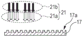
The light shielding film 9 has a plurality of light shielding regions 9A and a plurality of light transmitting regions 9A. In the example of fig. 2A, a light-shielding region 9A and a light-transmitting region 9A are formed by patterning a metal reflective film made of Al or the like on a transparent substrate 9b described later. The light-transmitting region 9A of fig. 2A corresponds to the light-transmitting regions 9A1, 9A2, 9A3, 9A4, and the like of fig. 2B, and the light-shielding region 9A of fig. 2A corresponds to the light-shielding regions 9A1, 9A2, 9A3, 9A4, and the like of fig. 2B. That is, the light shielding film 9 has a plurality of light shielding regions 9A and a plurality of light transmitting regions 9A in the in-plane direction (xy-plane) of the light shielding film 9. Each of the plurality of light-shielding regions 9A is opposed to one detector 10A. Each of the plurality of light-transmitting areas 9a is opposed to one detector 10 a. The plurality of light-shielding regions 9A (9A1 to 9A4) form a checkered pattern (see fig. 2B). The light-shielding regions 9A (9A 1-9A 4) may be formed in a pattern other than a checkered pattern, for example, a striped pattern.
A transparent substrate 9b made of SiO and disposed on the light incident side of the light shielding film 92And the like. The band-pass filter 9p is disposed on the light incident side of the transparent substrate 9b, and selectively makes only the wavelength λ in the incident scattered light 50Nearby light is transmitted.
The light 5 incident on the photodetector 13 passes through the band-pass filter 9p and the transparent substrate 9b, and reaches the light blocking region 9A where the reflective film is formed and the light transmitting region 9A where the reflective film is removed as the light 6A and 6A. The light 6A is shielded by the light shielding region 9A, and the light 6A passes through the light transmitting region 9A and is incident on the light coupling layer 12. The light 6a incident on the light coupling layer 12 is incident on the high refractive index transparent layer 12b via the low refractive index transparent layer 12 a. Gratings are formed at the upper and lower interfaces of the high refractive index transparent layer 12b, and as long as the pitch Λ of the gratings satisfies equation 2, waveguide light 6b is generated.
[ equation 2 ]
(formula 2)
Here, N is the effective refractive index of the waveguide light 6b, and θ is the incident angle with respect to the normal of the incident surface (xy surface). In fig. 2A, light is incident perpendicularly to the incident surface, and therefore θ is 0. In this case, the waveguide light 6b propagates in the x direction in the xz plane.
The components that have passed through the high refractive index transparent layer 12b and entered the lower layer generate waveguide light 6c under the same conditions as in expression 2 also in all the high refractive index transparent layers 12b located on the lower layer side due to the entry. In addition, although waveguide light is generated in practically all the high-refractive-index transparent layers 12b, waveguide light generated in 2 layers is representatively shown in fig. 2A. The waveguide light 6c generated on the lower layer side also propagates in the x direction in the xz plane. The waveguide lights 6b and 6c radiate light while propagating in the vertical direction at an angle θ (θ is 0 in the example of fig. 2A) with respect to the normal line of the waveguide surface (xy surface). The components of the radiated lights 6B1 and 6C1 traveling upward (toward the reflective film) directly below the light-shielding region 9A are reflected by the light-shielding region 9A and become lights 6B2 traveling downward along the normal line of the reflective surface (xy surface). The light 6B1, 6C1, 6B2 satisfies equation 2 with respect to the high refractive index transparent layer 12B, and therefore a part thereof becomes waveguide light 6B, 6C again. This waveguide light 6B, 6C also generates new radiated light 6B1, 6C1, and so on. As a whole, a component not becoming waveguide light passes through the light coupling layer 12 directly below the light transmitting region 9a, enters the microlens 10b as transmitted light 6d, and is detected by the detector 10 a. Immediately below the region 9A, a component that has become waveguide light is radiated, enters the microlens 10B as radiation light 6D, and is detected by the detector 10A.
The light-transmitting region 9a corresponds to the opening shown in fig. 1B. Through the light-transmitting region 9a, the light is branched to the detector directly below and the detectors on the left and right, respectively, and detected. If the detected light amounts of the detectors facing the light-transmitting regions 9a1, 9a2, 9A3, 9a4 and the light-shielding regions 9a1, 9a2, 9A3, 9a4 shown in fig. 2B are Q1, Q2, Q3, Q4, and Q1, Q2, Q3, Q4, respectively, the former 4 are the detected light amounts of light that has not become waveguide light and the latter 4 are the detected light amounts of light that has become waveguide light. The detector directly below the light-transmitting region 9a1 does not detect the light amount of light that has become waveguide light, and the detector directly below the light-shielding region 9a2 does not detect the light amount of light that has not become waveguide light. Here, at the detection position directly below the light-transmitting region 9a1, the detection light amount Q0 of light that has become waveguide light is defined as (Q1+ Q2+ Q3+ Q4)/4 (or Q0 is defined as (Q1+ Q2)/2), and at the detection position directly below the light-shielding region 9a2, the detection light amount Q of light that has not become waveguide light is defined as (Q1+ Q2+ Q3+ Q4)/4 (or Q0 is defined as (Q1+ Q2)/2). That is, in a certain region (light-shielding region or light-transmitting region), an average value of the light amounts detected at the detection positions directly below the regions adjacent to each other in the x direction and/or the y direction with the region as the center is defined. By applying this definition to all the regions, the detected light amount of light that has not become waveguide light and the detected light amount of light that has become waveguide light can be defined in all the detection regions (all the detectors constituting the photodetector 10) constituting the photodetector 10. The arithmetic circuit 11 performs the following arithmetic processing: in all the detectors constituting the photodetector 10, the detected light amount of light that has not become waveguide light and the detected light amount of light that has become waveguide light are defined as described above, and a value obtained by calculating the ratio of the detected light amount and the detected light amount for each detector is assigned to the pixel corresponding to each detector to generate an image or the like.
Next, a description will be given of a state in which the 1 pulse oscillation incident light is received by the photodetector 10 through the optical coupling layer 12. Fig. 3A is a sectional view similar to fig. 2A, and fig. 3B to H are time-series graphs based on the electromagnetic analysis results of the FDTD light intensity distribution plotted correspondingly to fig. 3A. The widths of the regions 9A and 9A in the x direction and the y direction were set to 5.6 μm, the depth of the grating in the z direction was set to 0.2 μm, and the high-refractive-index transparent layer (2 nd transparent layer) was set to Ta2O5The film had a z-direction thickness t1 of 0.34 μm and a low-refractive-index transparent layer (1 st transparent layer) of SiO2The thickness t2 in the z direction of the film was set to 0.22. mu.m.
In FIG. 3B, the wavelength λ of pulse oscillation is shown at a half-value width of 11fs (converted into a propagation distance of 3.3 μm)0The light 6a of 850nm passes through the light-transmitting region 9 a. In fig. 3C, the oscillation of the light 6a ends, and on the other hand, a waveguide propagating in the laminated high refractive index transparent layer 12b is generatedThe light 6b and 6c, components not being waveguide light, directly pass through the light coupling layer 12 and enter the microlens 10b (light 6 d). The waveguide light 6B, 6C radiates the light 6B1, 6C1 upward and downward while propagating below the light shielding region 9A in fig. 3D. On the other hand, the transmitted light 6d is collected by the microlens 10b to the detector 10 a. In fig. 3E, the transmitted light 6d enters the detector 10 a. On the other hand, the radiant lights 6B1, 6C1 and the reflected light 6B2 form a radiant light 6D, and are incident on the microlens 10B to be condensed. In fig. 3F to H, the transmitted light 6D and the radiated light 6D are condensed and incident on the detectors 10A and 10A, respectively. When the total light amounts detected by the detectors 10A, 10A are set to P0, P1, respectively, what shows the relationship between the value of P1/P0 and the coherence length of incident light is the curve 14A of fig. 4A. Where the coherence length is scaled by multiplying the pulse width (i.e., coherence time) by the speed of light. Further, the detected light amount P1 doubles the amount of received light in the detector 10A as a result of the analysis in fig. 3A to H. This is because the analysis detects only the radiation component from waveguide light 6B1 and the like, and actually adds the radiation component from similar waveguide light 6B 1' and the like propagated from the opposite side (see fig. 2B). The light amount ratio P1/P0 represents the light amount ratio of the component coupled with waveguide light and the component not coupled with waveguide light by the grating coupler (the optical coupler using the grating such as the structure of the high refractive index transparent layer (2 nd transparent layer) 12b shown in fig. 2A).
As is clear from FIG. 4A, the light intensity ratio P1/P0 is as small as about 0.2 at a coherence length of 1 μm or less and as large as about 1.3 at a coherence length of 10 μm or more, and monotonically increases with an increase in coherence length. That is, the light amount ratio P1/P0 strongly depends on the coherence (degree of interference) of incident light, is small for incoherent light such as sunlight (coherence length of 1 μm or less), increases as the interference of light increases, and is saturated in partially coherent light (coherence length of 10 μm or more). In addition, a curve 14A shows the result in the case where the light source is pulse-oscillated under the pulse condition (condition a) shown in fig. 4B. That is, the amplitude of the pulse constitutes an envelope of the gaussian distribution, and the phases are matched within the pulse width. At this time, the coherence length σ0Pulse width x speed of light. In contrast, curves 14B 1-14B 4 in FIG. 4C are shown in the figure4D, the pulse oscillation was performed under the pulse conditions. That is, although the amplitude of the pulse constitutes an envelope of the gaussian distribution, the phase changes with the peak of the gaussian distribution as a boundary Curves 14B 1-
14B 4 show phase differences, respectively The results were set to 0, π/4, π/2, and π. The coherence length in this case is represented by σ0Defined as pulse width x speed of light/2. In addition, the first and second substrates are,
 curve 14B1 under the condition (a) is the same as
 curve 14A, but the coherence length σ is0Because of the different definition of (a), the scale of the horizontal axis of the curve 14A is substantially halved. As shown in fig. 4C, with the phase difference The larger the size, the longer the coherence length the curve is. Although the phase difference between the adjacent wave trains is statistically between 0 and pi, it can be considered that the
 curve 14A, which is a characteristic of doubling the scale of the horizontal axis of the curve 14B1, is an average characteristic.
As is clear from fig. 3E to H, the waveguide lights 6b and 6c are not completely radiated in the range under the light shielding region 9A, and a part of the waveguide lights reach the range of the adjacent light transmitting region in the state of waveguide light. Since the radiation loss coefficient (ease of radiation of waveguide light) increases as the depth of the grating increases, the detected light amount P1 can be increased by increasing the depth of the grating in the region below the light shielding region 9A, and the modulation factor of the light amount ratio P1/P0 can be further increased.
Fig. 5A to D show the relationship of input light and coupled light in a grating coupler. In fig. 5A to D, a grating 17a is formed on the waveguide layer 17, and functions as a grating coupler as a whole. The waveguide layer 17 corresponds to the 2 nd transparent layer 12b in this embodiment mode. In fig. 5A, input light (waveguide light 18 propagating in the waveguide layer 17) is separated into 3 coupled lights, i.e., waveguide light 19a and radiated lights 19b, 19c, by the grating coupler. According to the inverse theorem in the waveguide theory, as shown in fig. 5B, if backward waves with respect to the 3 coupled lights in fig. 5A, that is, waveguide light 18A and incident lights 18B, 18C (pumping) are simultaneously inputted, waveguide light 19A is generated with 100% efficiency. On the other hand, as shown in fig. 5C, when the backward waves of 2 out of the 3 coupled lights in fig. 5A, that is, the waveguide light 18A and the incident light 18C are inputted at the same time (double pumping), waveguide light 19A and transmitted light 19B are generated, and the light amount of the waveguide light 19A is gradually decreased. Further, as shown in fig. 5D, when only the incident light 18C (single pump) which is a backward wave with respect to 1 of the 3 coupled lights in fig. 5A is inputted, waveguide light 19A and transmitted light 19B are generated, and the light amount of the waveguide light 19A further decreases. That is, the input efficiency to the waveguide light 19A is decreased in the order of fig. 5B, 5C, and 5D.
Fig. 6A to J show the principle that the light quantity ratio P1/P0 strongly depends on the coherence length of incident light. In fig. 6A to J, a grating 17a is formed on the waveguide layer 17, and functions as a grating coupler as a whole. Fig. 6A to E show a case where the coherence length of incident light is long, and arrows 20a (broken line), 20b (solid line), and 20c (black line) dividing 1 wave train 20 into 3 segments show how it propagates and branches with the passage of time. Fig. 6F to J show a case where the coherence length of incident light is short, and arrows 21a (solid line) and 21b (black line) dividing 1 wave train 21 into 2 segments show how the incident light propagates and branches with the passage of time. The long wavelength train 20 is incident on the grating coupler in fig. 6A, and weak guided light (shown by 1 dashed arrow respectively) is generated in fig. 6B by the single pump at the position 22a where there are two, and the rest is transmitted (shown by 2 dashed arrows respectively). In fig. 6C, the light is split into a weakly waveguided light (shown with 1 solid arrow) and a strongly transmitted light (shown with 2 dashed arrows) by a single pump at position 22 a. Further, by the double pumping at the position 22b, strong waveguiding light (shown by 1 dotted arrow and 2 solid arrows) and weak transmitting light (shown by 1 solid arrow) are divided. At position 22b, waveguide light propagating from the left side is added to incident light from above, and thus the two-pump operation is performed. In fig. 6D, the light is split into weak waveguided light (shown by the 1 black arrow) and strong transmitted light (shown by the 2 black arrows) by the single pump at position 22a, and into strong waveguided light (shown by the 1 solid arrow and the 2 black arrows) and weak transmitted light (shown by the 1 black arrow) by the double pump at position 22 b. Propagation of the waveguide light and the transmitted light in fig. 6D continues in fig. 6E. When the light amount ratio P1/P0 is estimated by the number of arrows, the number of arrows (23b) serving as waveguide light is 8, whereas the number of arrows (23a) serving as transmission light is 10, and P1/P0 is 8/10 which is 0.80. On the other hand, in fig. 6F and 6G, the short wave train 21 enters the grating coupler, and in fig. 6H, weak wave guided light (shown by 1 solid arrow) is generated by the single pump at two positions 22a, and the rest is transmitted (shown by 2 solid arrows). In fig. 6I, the light is split into weakly waveguided light (shown with 1 black arrow 1) and strongly transmitted light (shown with 2 black arrows) by a single pump at position 22 a. Further, by the double pumping at the position 22b, strong waveguiding light (shown by 1 solid arrow and 2 black arrows) and weak transmitting light (shown by 1 black arrow) are divided. At position 22b, the incident light from above is added with waveguide light propagating from the left side thus becoming double pumped. Propagation of the waveguide light and the transmitted light in fig. 6I continues in fig. 6J. When the light amount ratio P1/P0 is estimated by the number of arrows, the number of arrows (24b) that become waveguide light is 5, whereas the number of arrows (24a) that become transmission light is 7, and P1/P0 is 5/7, which is 0.71. Therefore, the probability of double pumping is increased when the coherence length of the incident light is longer, and it is found that the light amount ratio P1/P0 is larger.
Fig. 7 shows a pattern of the wave train incident on the opening 9a shown in fig. 1B. If it is assumed that a fixed coherence length sigma is emitted by the light source 20Because the coherence length does not change in the subject 4, the wave trains 15a and 15b incident on the aperture 9a all have the same coherence length σ0The light enters the aperture 9a at different timings according to the wave train by scattering. As shown in FIG. 7, if 2 wave trains 15a and 15b (after the wave trains 15a and 15b, the wave trains 15a and 15b are connected with the same coherence length and different phases), the phases are randomWhen the light is continuously incident while being shifted, they interfere with each other to form 3 wave trains 15A, 15B, and 15C. The wave train 15C is a wave train in which the wave trains 15a and 15b overlap and interfere with each other. The wave trains 15A and 15B are the remaining portions where the wave train 15A and the wave train 15B do not overlap each other. The wave trains 15A, 15B, and 15C have the same wavelength, but there is no phase correlation between them, and the length of the wave trains is longer than the original σ0Short. The wavelength spread (longitudinal mode width) of the synthesized waves (wave trains 15A, 15B, 15C) is the same as that of the original wave trains 15A, 15B. That is, the coherence length defined in the temporal coherence does not change (see fig. 5A to D). On the other hand, if the coherence length is defined as the continuity of the wave, that is, the length of the wave with continuous phase, the coherence length of the composite wave becomes shorter. Hereinafter, the coherence length defined in this sense is referred to as "effective coherence length", and the coherence length defined by temporal coherence is referred to as "coherence length", respectively. Without the effect shown in fig. 7, the effective coherence length is equal to the coherence length. The effective coherence length must be equal to or shorter than the coherence length. As the coherence length becomes shorter, the effective coherence length also becomes shorter. In addition, spatial coherence deteriorates and the effective coherence length also becomes short. The coherence length in the description of fig. 3A to H, fig. 4A to D, and fig. 6A to J all mean the effective coherence length. That is, the light amount ratio P1/P0 of fig. 4A strongly depends on the effective coherence length of incident light.
Fig. 8A and B are explanatory diagrams showing how the variation in the optical path length (phase) of the incident light entering the opening 9a correlates with the attenuation of the effective coherence length. Using a ray tracing method such as Monte Carlo method, the group of rays incident on the opening 9a can be statistically processed on the premise of continuous oscillation. For example, if it is assumed that many light rays are emitted from the light source 2 and there are n light rays incident to the opening 9a, the optical path length of the k-th light ray among them is set to sk(k ═ 1, 2, … …, n). As shown in fig. 8A, z is a distance in the propagation axis direction, and the optical path length s iskThe statistical distribution of (b) is represented by (f), (z), and the waveform of the incident intensity of the light (the waveform obtained by multiplying the time change of the light intensity by the light velocity and replacing the time change by the distance unit) is given by (g), (z). If the decay of the effective coherence length in FIG. 7 is statistically processedThe principle of subtraction is that the wavetrain g (z-z) is relative to the wavetrain g (z) serving as the reference0) Probability μ within the same wave traindGiven by formula 3,. mu.dRepresenting the attenuation ratio of the effective coherence length. Wherein g (z) is defined by formula 4, σ0Is the coherence length of the light emitted by the light source. Equation 5 holds when m and σ are the average and standard deviation of the optical path length, and f (z) is a normal distribution.
[ equation 3 ]
(formula 3)
[ equation 4 ]
(formula 4)
[ equation 5 ]
(formula 5)
The curve 16 of FIG. 8B represents the attenuation ratio μdAnd the standard deviation sigma of the sum optical path length with respect to the effective coherence length sigma0Ratio of (a/a)0The calculation result of the relationship between them. Shows the companion sigma/sigma0Increase of attenuation ratio mudAnd becomes smaller. When f (z) is not a normal distribution, the curve 16 has another characteristic.
The relationship between fig. 8A and B is established when the light source oscillates continuously, but is also approximately established when the pulse oscillation is performed as long as the deviation of the optical path length is approximately equal to the pulse length (a value obtained by multiplying the pulse time width by the light speed). In addition, when the phase difference between close wave trains is small from the definition of the effective coherence length, these wave trains should be regarded as one wave train, but equation 3 ignores this. Therefore, the relationship between fig. 8A and B excessively deals with the influence of the attenuation of the effective coherence length, and the following discussion will be made based on the relationship between fig. 8A and B.
FIGS. 9A to C are tablesAn explanatory diagram showing the principle of the change in the internal coherence length of the subject 4 is shown. The models of fig. 8A and B represent degradation of effective coherence (e.g., degradation of spatial coherence), while the models of fig. 9A-C represent degradation of temporal coherence. As shown in fig. 9A, consider the following case: wavelength lambda0At refractive index n0Repeats scattering n times, and by scattering the kth time, light is incident on the radius r0The spherical reflector 26. Coherence length of light is σkThe y-axis incident position on the spherical reflector 26 is ykThe angle of incidence with respect to the normal to the spherical surface of the spherical reflector 26 is phikThe x-axis is defined in correspondence with the propagation orientation of the light. It is assumed that both incidence and reflection occur in the same plane including the center 26a of the sphere. If the y-axis position of the wave train 25 is from ykBecomes yk+ΔykThen angle phikChange to phik+Δφk. As shown in fig. 9B, when the reflector 26 is stationary, the coherence length of the reflected wave train 27 does not change. As shown in fig. 9C, when the reflector 26 moves in the xy plane (the y component of the moving speed is denoted by v) while the wave train 25 is reflected by the reflector 26, the wave train is separated into 2 wave trains of the wave train 27a and the wave train 27b after the reflection. These wave trains 27A and 27B are emitted from the inside of the subject to the outside, pass through the condenser lens 7 with the focal distance f, become converging light 27A and 27B, and are converged on the detection pixel surface 9a to form the center interval δkThe focal points ( intensity distributions 28A, 28B). When the numerical aperture of the condenser lens 7 is NA, the diameter of the condensing point is λ0the/NA is given. The amount Δ y of displacement during reflection of the wave train on the reflector 26kGiven by equation 6 (c is the speed of light).
[ equation 6 ]
(formula 6) Δ yk=vσk/c
If the cosine of the scattering angle in the k-th scattering is set as gkThen is in gk、φk、δkThe relationships among equation 7, equation 8, and equation 9 hold. Wherein n is0Is the refractive index of the object.
[ equation 7 ]
(formula (II)7)
[ equation 8 ]
(formula 8)
[ equation 9 ]
(formula 9)
On the other hand, ykAt an angle phikThere is a relationship of equation 10, Δ φkGiven by equation 11.
[ equation 10 ]
(formula 10)
[ equation 11 ]
(formula 11)
At the centre of the spot separation deltakSpecific point diameter (lambda)0NA) is larger, it is considered that 2 wave trains 27A and 27B (or 27A and 27B) are separated and the coherence length is divided into 2 pieces without interference between 2 points. Therefore, Δ given by equation 12 is usedkThe number of divisions of the wave train caused by the kth scattering is 2 DeltakThe k +1 th coherence length is given by equation 13.
[ equation 12 ]
(formula 12)
[ equation 13 ]
(formula 13)
Since scattering is repeated n times inside the object 4, the attenuation ratio μ of the coherence lengthi(final coherence length σ)nRelative to the initial coherence length σ0The ratio) is given by equation 14.
[ NUMBER FORM 14 ]
(formula 14)
When the subject 4 is a living body, the anisotropic scattering coefficient is said to be 0.9. This value corresponds to the condition of particle size parameter (2 π reflector radius/wavelength) 1 in the Mie scattering of the dielectric sphere. Based on this condition, the reflector radius is considered to be 0.2 × wavelength. For example, if f is 200mm, NA is 0.1, v is 10mm/s, and c is 3 × 1011mm/s,σ0=6mm,λ0=0.85×10-3mm,n01.37 (condition D), then ΔkGiven by equation 15.
[ equation 15 ]
(formula 15)
ΔkThe value is about 0.1, and the coherence length is roughly halved by about 10 scattering orders.
The forward scattering in the model of FIGS. 9A to C corresponds to 2 φkGreater than pi/2, back scattering is equivalent to 2 phikIs less than pi/2. According to formula 11, at phikΔ φ in case of > π/2 (forward scattering)kBecome larger and at 2 phikDelta phi in the case of < pi/2 (back scattering)kAnd becomes smaller. Therefore, according to expressions 12 and 13, the coherence length is likely to be deteriorated when the amount of forward scattering is large, and the coherence length is less likely to be deteriorated when the amount of backward scattering is large.
Fig. 10A to H are diagrams showing results calculated by a ray tracing method based on the monte carlo method assuming that a human head is an object. Fig. 10A shows the overall optical arrangement and the state of ray tracing, and fig. 10B to G show the results obtained by dividing the image 8B at the detection position into 20 × 20 regions and analyzing the regions. Fig. 10B shows a light intensity distribution, fig. 10C shows an optical path length average distribution, fig. 10D shows an optical path length standard deviation distribution, fig. 10E shows an intra-subject coherence length attenuation distribution (calculation result of equation 14), fig. 10F shows a distribution obtained by multiplying the value of each region in fig. 10D by the value of each region in fig. 10B, fig. 10G shows a distribution obtained by dividing the value of each region in fig. 10F by the value of each region in fig. 10E, and fig. 10H shows an on-x-axis distribution diagram (regions 3 to 18 in which the x-axis direction is shown) of the value obtained by averaging the y-axis component in fig. 10D, E over the range from region 3 to region 18 in the y-axis direction. The human head was composed of a scalp 4a, a skull 4b, a CFS layer 4c, a gray substance 4d, and a white substance 4e, and table 1 shows the absorption coefficient (1/mm), the scattering coefficient (1/mm), the anisotropic scattering parameter, and the film thickness (mm), respectively.
[ TABLE 1 ]

As shown in fig. 10A, the gray substance 4D and the white substance 4E are at the same depth, and the regions are divided by the positive and negative of the x-axis, the analysis region is 40mm × 40mm in the xy direction, 47mm in the z direction, and the light propagated beyond this region is excluded from the calculation, the incident light 3 assumes light that is incident perpendicularly at 3 × 3 positions each separated by 10mm in the x direction and the y direction on the surface of the scalp 4a, the detection sets the condenser lens 7 at a position separated by 1000mm from the surface of the scalp 4a, and based on the light taken with the object-side numerical aperture (sin α) set to 0.1, the image 8B of the image plane position is calculated (other conditions are in accordance with condition D), the darker (less) of the periphery of fig. 10B is because the light exceeding the analysis region is excluded from the calculation, the light becomes brighter (less intense) near the incident position of the light in fig. 10B, the white substance is seen as a little darker (B, C, D) near the incident position of the light in the left half, the white substance is seen as a less bright (as a left half) than the average of the left half of the white substance, the right half-side, the white substance 4D is seen as a less bright (10E) in fig. 10C, the left half of the white substance is seen as a left half-side, the average of the left half-white substance, the left-white substance 4D is seen as a white substance, the left-half-white substance, the average of the right half-white substance is seen as a white substance, the right half-white substance, the white substance is seen as a white substance, the white substance 3, the right-half-white substance is seen as a white substance, the right.
When fig. 8A and B, fig. 9A to C, and fig. 10A to H are combined, it can be said that the case is as follows in fig. 4A. That is, when the coherence length when the light source is emitted is 6mm, the coherence length is attenuated to 6.0 × 0.29 to 1.74mm in the left half (on the side of white matter 4 d) and 6.0 × 0.34 to 2.04mm in the right half (on the side of white matter 4E) by scattering inside the object according to fig. 10E. Further, according to FIG. 10D, the deviation of the optical path length is σ/σ in the left half 026/1.74-14.9, sigma/sigma in right half 021/2.04 equals 10.2 (see fig. 4A). Thus, according to FIG. 8B, the effective coherence length attenuation ratio μd0.00020 in the left half and 0.00043 in the right half. Therefore, the effective coherence length of the detected light is 6mm × 0.00020 ═ 1.2 μm, and 6mm × 0.00043 ═ 2.6 μm, respectively. It is understood that, in fig. 4A, detection signals having values of P1/P0 of 0.3 and 0.6 can be obtained from the intersection of the curve 14A and the straight line 14A having an effective coherence length of 1.2 μm and the intersection of the curve 14A and the straight line 14b having an effective coherence length of 2.6 μm, respectively. That is, it is understood that the distribution of the gray-white substance 4d and the white substance 4e located inside the skull 4b can be detected from the detection signals P1/P0 in the light detection device 13 according to the present embodiment. The distribution of the detection signal P1/P0 is similar to that of FIG. 10F, G, and differentiation between the left half side (x < 0) and the right half side (the left half side is smaller than the right half) can be achieved. Further, the positions of the straight lines 14A and 14b may be detected, that is, the effective coherence length of the detection light may be detected so as to be separated from each other to the left and right with respect to the fluctuation portion (the range of the effective coherence length 1 to 10 μm) of the curve 14A. The positions of the straight lines 14a, 14b can be freely adjusted as long as the coherence length of the light source can be made variable. By analyzing the detection signals P1/P0 corresponding to the coherence length of the light source, the structure of the object can be efficiently analyzed. Further, it is possible to prevent the occurrence of,as in fig. 10F, as the structure difference can be clearly obtained by multiplying the light intensity distribution by the standard deviation distribution of the optical path length, which is the amount related to the detection signals P1/P0, the detection signals P1/P0 are multiplied by other detection signals (for example, the detection signal P0 or the detection signal (P0+ P1)), or compared, and various arithmetic processing is applied thereto, whereby a signal having a higher S/N ratio can be obtained. These arithmetic processing for increasing S/N may be performed in accordance with the light emission intensity of the light source or the aperture of the lens (i.e., the amount of light entering the photodetection device 13) when changed, or may be performed in accordance with the movement speed v of the scattering body when the emission direction of the light source is changed because equation 15 is related to the movement speed v of the scattering body.
Although the coherence length of about 6mm is short as a laser beam, it is in a practical range for a light source which is multispectral for reducing coherence, such as a high-frequency-superposition semiconductor laser or a self-pulsation semiconductor laser. A semiconductor laser driven by a high-frequency superimposing circuit (generally, a frequency of 300 MHz) oscillates with a coherence length in a range of 0.1mm to 0.2mm, and the coherence length can be varied in a range of 0.2mm to several tens of mm by changing the frequency, amplitude, or the like of the superimposing circuit (for example, reducing the frequency). In addition, in the case of a scanning light source (a light source that periodically scans the wavelength of laser light in the range of several tens of nm), the coherence length can be varied in the range of 0.3mm to several tens of mm by changing the wavelength variation width or the periodic frequency. However, in the case of using a scanning light source, the band-pass filter 9p is used as the case may be, in order to limit the wavelength of light incident on the light coupling layer 12. Further, a light source having a wide line width such as an LED and a band-pass filter having a narrow band are combined to obtain a desired coherence length. In this case, the band pass filter may be disposed between the light source and the object or between the object and the optical coupling layer. Alternatively, 2 or more light sources having different wavelengths may be used as the light source. When these lights are scattered in the subject and enter the opening 9a, beat frequencies are generated by the principle described in fig. 15C, and the coherence length becomes short. As effectively a light source with a short coherence length is used. In this case, however, the band-pass filter 9p is used as appropriate in order to limit the wavelength of light incident on the light coupling layer 12. In addition, when light sources having different wavelengths are used, when the emission intensity ratio of the light source is changed, the emission pattern of the beat frequency is also changed, and the distribution of the effective coherence length is also changed. Therefore, the detection signal P1/P0 may be subjected to arithmetic processing according to a change in the emission intensity ratio of the light source to increase S/N.
In addition, a pulsed light source may be used as the light source. At this time, the coherence length is equal to the pulse length (a value obtained by multiplying the pulse time width by the speed of light). In the case of the pulsed light source, the relationship of temporal coherence deterioration shown in fig. 9A to C holds. On the other hand, in the case of a pulsed light source, the superposition of wave trains is reduced (the probability that a certain wave train is within the same wave train as a reference wave train is reduced). Therefore, the effect of shortening the effective coherence length as described in fig. 8B is reduced. In this case, the pulse time width is selected so that the positions of the straight lines 14A and 14b (effective coherence length of the detection light) in fig. 4A fall within the fluctuation part (range of 1 to 10 μm) of the curve 14A.
When the light detection device of the present embodiment is used in this manner, the difference between the gray-white substance 4d and the white substance 4e located inside the skull 4b can be detected as the output difference of the electric signal in the subject shown in fig. 10A to H. This can significantly improve the S/N as compared with the method of detecting the light intensity distribution image shown in fig. 10B (conventional example 2).
(embodiment 2)
In the present embodiment, the configuration for guiding the waveguide light 6b generated in the 2 nd transparent layer 12b to the detector 10A is different, and the other configurations are all the same as those in embodiment 1, and therefore the same reference numerals are given to common elements, and detailed description thereof is omitted.
Fig. 11A, B shows a sectional configuration of the grating 12d and the waveguide layer (2 nd transparent layer) 12b for guiding the waveguide light 6b to the detector 10A. Fig. 11A is a cross-sectional view of a pixel including a position near the central axis (on-axis position) of the condenser lens 7 in fig. 1A, and fig. 11B is a cross-sectional view of a pixel including a position outside the axis of the condenser lens 7. In this embodiment, the center of the light-transmitting region 9A (light-shielding region 9A) is arranged to be offset from the center of the detector 10A (10A) at the off-axis position of the condenser lens 7. In the present disclosure, the phrase "the detector is disposed to face the light blocking region or the light transmitting region" also includes a configuration in which the detector is disposed so that the center positions thereof are offset as in the present embodiment. The grating 12d has different pitch conditions in fig. 11A and 11B. That is, fig. 11A shows a pitch (═ Λ 1) when θ ≠ 0 is set in equation 2, and fig. 11B shows a pitch (═ Λ 2) when θ ≠ 0 is set. Therefore, the waveguide light 6B is generated in both the left and right directions on the paper surface in fig. 11A, and the waveguide light 6B is generated in either the left or right direction in fig. 11B (right side in the drawing), and is radiated directly below the light shielding region 9A to become radiation light 6D and enter the detector 10A. The value of θ in equation 2 is determined according to the incident angle of the light from the condenser lens 7. In embodiment 1, it is necessary to use an image side telecentric lens for the condenser lens 7, but in embodiment 2, it is not necessary, and therefore, the lens cost can be suppressed.
Fig. 11C is a diagram showing another mode of guiding the waveguide light 6b to the detector 10A. While the grating 12d is formed over the entire surface in embodiment 1, the grating 12d is formed only directly below the light-transmitting region 9a in fig. 11C. The waveguide layer (the 2 nd transparent layer) 12b is gently bent toward the detector 10A side directly below the light shielding region 9A, and the waveguide light 6b is also bent (waveguide light 6b1) along the waveguide layer (the 2 nd transparent layer) 12b, is radiated from the end face of the waveguide layer (the 2 nd transparent layer) 12b, becomes radiation light 6D, and enters the detector 10A. Although the manufacturing process is complicated by bending the waveguide layer (2 nd transparent layer) 12b, detection with less optical loss can be expected as compared with embodiment 1.
Fig. 11D is a diagram illustrating a different pattern of the reflective film to be the light shielding region 9A. In embodiment 1, for the light-transmitting region 9A (or the light-shielding region 9A), 1 microlens 10B (or 10B) and 1 detector 10A (or 10A) correspond, and in this embodiment, 2 microlenses 10B and 10B '(or 10B and 10B'), 2 detectors 10A and 10A '(or 10A and 10A') correspond. The 2 detectors 10A and 10A '(or 10A and 10A') are electrically conducted. In this embodiment, the length of the grating coupler in the traveling direction of the waveguide light 6b (coupling length of light) is increased. According to the principle illustrated in fig. 6A to J, if the grating coupler is made longer, the probability of causing double pumping is also likely to be different for incident light having a longer coherence length. That is, there is an advantage that the light amount ratio shown in fig. 4A becomes larger than the range in which P1/P0 is changed. In the embodiment of fig. 11D, the light-transmitting region 9A and the light-shielding region 9A have a width in the xy plane of 5.6 μm × 2 μm, and the result calculated assuming that the light source oscillates under the pulse condition (condition a) shown in fig. 4B is represented as a curve 14C (condition C) of fig. 4A. Since the coupling length of light (the width of the light-transmitting region 9a) is increased, the curve 14C is shifted to the side where the coherence length is longer than the curve 14A. The light-transmitting region 9A (or the light-shielding region 9A) may correspond to 3 or more microlenses 10B (or 10B) and detectors 10A (or 10A). Further, the pattern formation of the reflective film (light-shielding region 9A) may be performed by combining patterns having different pitches. For example, in fig. 11E, the light-transmitting region 9A (or the light-shielding region 9A) forms 2 checkered patterns with different pitches, and in fig. 11F, forms 2 stripe patterns with different pitches. In any case, the number of microlenses and detectors corresponding to 1 light-transmitting region 9A (or light-shielding region 9A) is larger in the pattern having a wider pitch than in the pattern having a narrower pitch. For example, in a pattern with a narrow pitch, 1 microlens and 1 detector are provided for 1 light-transmitting region 9A (or light-shielding region 9A) in the x-axis direction. In the pattern having a wide pitch, 2 microlenses and 2 detectors are provided for 1 light-transmitting region 9A (or light-shielding region 9A) in the x-axis direction. The orientation of the grating vector of the grating is made parallel to the x-axis direction, but may be changed depending on the location.
(embodiment 3)
In the present embodiment, the signal arithmetic circuit 11 is different in arithmetic method, and other configurations are the same as those in embodiments 1 and 2, so that the same elements are assigned the same reference numerals, and detailed description thereof is omitted.
Fig. 12 is an explanatory diagram showing a relationship between the oscillation of the light source 2 and the detection signal in the present embodiment. The light source 2 oscillates a pulse 3a under the control of the control circuit 1, and this light 3 is scattered inside the object 4, received by the detectors 10A, 10A via the light-transmitting region 9a, and detected as a signal 63 with the vertical axis as the detection intensity and the horizontal axis as the elapsed time. When the light amount detected by the detector 10A is P0 and the light amount detected by the detector 10A is P1, the signal 63 corresponds to the light amount P0 (or P0+ P1). The signal 63 has a larger time width than the original pulse 3a due to the influence of the dispersion of the optical path length caused by scattering. The first output 63a of the signals 63 is a signal of the light 5a1 reflected on the surface of the object 4. The output 63c of the signal 63 during the time t1 to t2 is a signal of the light 5a2, 5a3 scattered inside the object 4. While the optical path lengths are equal for light 5a2 and 5a3, light 5a2 is scattered more backward and traces an optical path propagating near the surface layer, whereas light 5a3 is scattered less backward and traces an optical path reaching the deep layer. In the explanation of fig. 9A to C, it is known that the coherence length is likely to deteriorate when the amount of forward scattering is large, and the coherence length is less likely to deteriorate when the amount of backward scattering is large. Therefore, the ratio of the forward scattering to the backward scattering is reflected in the light amount ratio P1/P0 of the light 5a2 and the light 5a 3. In the present embodiment, the arithmetic circuit 11 detects the output 63c by time-division of the signal 63 and generates an image. That is, light in the time period t1 to t2 at which the internally scattered light 5a2, 5a3 arrives is detected, and an image is generated as intensity distribution information for each detector. Further, the arithmetic circuit 11 distinguishes the image based on the output 63c according to the value of the light amount ratio P1/P0. Specifically, for example, the 1 st image is generated based on pixels having a light amount ratio P1/P0 equal to or greater than a certain threshold. That is, the 1 st image is generated as the distribution information of the light amount detected by the detector corresponding to the pixels having the light amount ratio P1/P0 of a certain threshold or more. Further, the 2 nd image based on the pixels having the light amount ratio P1/P0 smaller than a certain threshold may be generated. That is, the 2 nd image may be generated as the distribution information of the light amount detected by the detector corresponding to the pixels having the light amount ratio P1/P0 smaller than a certain threshold value. In the 2 nd conventional example, the light 5a2 and the light 5a3 are not distinguished, but the ratio of forward scattering to backward scattering is reflected in the detection light amount ratio P1/P0 in the present embodiment, so that the light 5a2 and the light 5a3 can be distinguished, and the inside of the object 4 can be analyzed according to the depth. In addition, as in embodiment 1, the detection signal P1/P0 may be multiplied by another detection signal (for example, the detection signal P0 or the detection signal (P0+ P1)) or compared to perform various arithmetic processing. Further, the output 63c may be subjected to arithmetic processing with the detection signals P1/P0 or other detection signals.
Description of the reference symbols
100 light detection system
1 control circuit
2 light source
3 incident light to the object
4 object
5. 5A, 5A scattered light
7 condensing lens
8a substantial object (aggregation of object points)
8b image of image plane position
9 light-shielding film
9a open, light-transmitting area
9A light-shielding region
10 photo detector
11 arithmetic circuit
12 optical coupling layer
13 photo detector
Claims (21)
1. A light detection device is provided with:
a photodetector having a main surface, including at least 1 st detector and at least 1 nd 2 detector arranged along the main surface;
a light coupling layer disposed on the photodetector, the light coupling layer including a1 st low refractive index layer, a1 st high refractive index layer disposed on the 1 st low refractive index layer and including a1 st grating, and a2 nd low refractive index layer disposed on the 1 st high refractive index layer, the 1 st high refractive index layer having a refractive index higher than refractive indices of the 1 st low refractive index layer and the 2 nd low refractive index layer; and
a light shielding film disposed on the light coupling layer and including at least 1 light transmitting region and at least 1 light shielding region adjacent to the at least 1 light transmitting region,
the 1 st high refractive index layer is disposed between the photodetector and the light shielding film.
2. The light detection arrangement of claim 1,
the at least 1 light-transmitting region corresponds to the at least 1 st detector,
the at least 1 light-shielded region corresponds to the at least 12 nd detector.
3. The light detection arrangement of claim 1,
the at least 1 light-transmissive region is opposed to the at least 1 st detector,
the at least 1 light-shielding region is opposite to the at least 12 nd detector.
4. The light detection arrangement of claim 3,
the at least 1 st detector is provided with a plurality of 1 st detectors,
the at least 12 nd detector is provided with a plurality of 2 nd detectors,
the plurality of 1 st detectors and the plurality of 2 nd detectors are two-dimensionally arranged along the main surface,
the at least one light-transmitting region is provided with a plurality of light-transmitting regions,
the at least one light-shielding region is provided with a plurality of light-shielding regions,
each of the plurality of light-transmissive regions opposes at least one 1 st detector of the plurality of 1 st detectors,
each of the plurality of light-shielding areas opposes at least one 2 nd detector of the plurality of 2 nd detectors.
5. The light detection arrangement of claim 4,
the plurality of light-shielding regions are arranged in a stripe pattern or a checkerboard pattern in a plan view.
6. The light detection arrangement of claim 1,
the light detector further includes:
a1 st microlens disposed between the at least one 1 st detector and the light coupling layer; and
a2 nd microlens disposed between the at least one 2 nd detector and the light coupling layer.
7. The light detection device according to any one of claims 1 to 6,
the light coupling layer further includes:
a3 rd low refractive index layer; and
a2 nd high refractive index layer disposed between the 3 rd low refractive index layer and the 1 st low refractive index layer, and the 2 nd high refractive index layer includes a2 nd grating,
the 2 nd high refractive index layer has a refractive index higher than those of the 1 st low refractive index layer and the 3 rd low refractive index layer.
8. An optical detection system comprises an optical detection device and a light source,
the light detection device includes:
a photodetector having a main surface, including at least 1 st detector and at least 1 nd 2 detector arranged along the main surface;
a light coupling layer disposed on the photodetector, the light coupling layer including a1 st low refractive index layer, a1 st high refractive index layer disposed on the 1 st low refractive index layer and including a1 st grating, and a2 nd low refractive index layer disposed on the 1 st high refractive index layer, the 1 st high refractive index layer having a refractive index higher than refractive indices of the 1 st low refractive index layer and the 2 nd low refractive index layer; and
a light shielding film disposed on the light coupling layer and including at least 1 light transmitting region and at least 1 light shielding region adjacent to the at least 1 light transmitting region,
the 1 st high refractive index layer is disposed between the photodetector and the light shielding film.
9. The light detection system of claim 8,
the at least 1 light-transmitting region corresponds to the at least 1 st detector,
the at least 1 light-shielded region corresponds to the at least 12 nd detector.
10. The light detection system of claim 8,
the at least 1 light-transmissive region is opposed to the at least 1 st detector,
the at least 1 light-shielding region is opposite to the at least 12 nd detector.
11. The light detection system of claim 8,
further comprises an arithmetic circuit for calculating the time of the operation,
the arithmetic circuit calculates a ratio of a1 st signal detected by the at least one 1 st detector to a2 nd signal detected by the at least one 2 nd detector.
12. The light detection system of claim 8,
further comprises an arithmetic circuit for calculating the time of the operation,
the arithmetic circuit calculates at least 1 selected from the group consisting of a ratio of the 1 st signal to the 2 nd signal detected by the at least one 1 st detector and a ratio of the 2 nd signal to the 1 st signal in the sum, and a ratio of the 2 nd signal in the sum.
13. The light detection system of claim 11,
the at least one 1 st detector is provided with a plurality of 1 st detectors,
the at least one 2 nd detector is provided with a plurality of 2 nd detectors,
the plurality of 1 st detectors and the plurality of 2 nd detectors are two-dimensionally arranged along the main surface,
the at least one light-transmitting region is provided with a plurality of light-transmitting regions,
the at least one light-shielding region is provided with a plurality of light-shielding regions,
each of the plurality of light-transmissive regions opposes at least one 1 st detector of the plurality of 1 st detectors,
each of the plurality of light-shielding areas opposes at least one 2 nd detector among the plurality of 2 nd detectors,
the arithmetic circuit generates an image representing a distribution of the ratios in the photodetector by calculating the ratios for each of the plurality of 1 st detectors.
14. The light detection system of claim 12,
the at least one 1 st detector is provided with a plurality of 1 st detectors,
the at least one 2 nd detector is provided with a plurality of 2 nd detectors,
the plurality of 1 st detectors and the plurality of 2 nd detectors are two-dimensionally arranged along the main surface,
the at least one light-transmitting region is provided with a plurality of light-transmitting regions,
the at least one light-shielding region is provided with a plurality of light-shielding regions,
each of the plurality of light-transmissive regions opposes at least one 1 st detector of the plurality of 1 st detectors,
each of the plurality of light-shielding areas opposes at least one 2 nd detector among the plurality of 2 nd detectors,
the arithmetic circuit calculates, for each of the 1 st detectors, at least 1 selected from a group consisting of the ratio of the 1 st signal to the sum and the ratio of the 2 nd signal to the sum, and thereby generates an image showing a distribution of at least one of the photodetectors selected from a group consisting of the ratio of the 1 st signal to the sum and the ratio of the 2 nd signal to the sum.
15. The light detection system according to any one of claims 8 to 14,
the light source emits pulsed light.
16. The light detection system according to any one of claims 8 to 14,
the photodetection device further includes a band-pass filter disposed on the optical coupling layer and selectively transmitting a wavelength of the light emitted from the light source.
17. The light detection system according to any one of claims 8 to 14,
the device is also provided with a control circuit,
the control circuit changes a coherence length of light emitted from the light source.
18. The light detection system of claim 13,
the device is also provided with a control circuit,
the control circuit varies a coherence length of light emitted from the light source,
the arithmetic circuit generates the image representing the distribution of the ratio values for each coherence length changed by the control circuit.
19. The light detection system of claim 14,
the device is also provided with a control circuit,
the control circuit varies a coherence length of light emitted from the light source,
the arithmetic circuit generates the image indicating a distribution of at least one selected from the group consisting of the ratio of the 1 st signal in the sum and the ratio of the 2 nd signal in the sum for each coherence length changed by the control circuit.
20. The light detection system of claim 13,
the operation circuit is used for carrying out the operation,
calculating the ratio for each of the plurality of 1 st detectors using the 1 st signal detected by the plurality of 1 st detectors and the 2 nd signal detected by the plurality of 2 nd detectors within a predetermined time range,
a1 st image showing the distribution of the 1 st signal detected by a1 st detector among the 1 st detectors, the ratio of which is equal to or greater than a threshold, within the predetermined time range, and a2 nd image showing the distribution of the 1 st signal detected by a1 st detector, the ratio of which is less than the threshold, within the predetermined time range are generated.
21. The light detection system of claim 14,
the operation circuit is used for carrying out the operation,
using the 1 st signal detected by the 1 st detectors and the 2 nd signal detected by the 2 nd detectors within a predetermined time range, calculating, for each of the 1 st detectors, at least 1 selected from the group consisting of the ratio of the 1 st signal to the sum and the ratio of the 2 nd signal to the sum,
and generating a1 st image and a2 nd image, the 1 st image showing a distribution of the 1 st signal detected in the predetermined time range by a1 st detector in which the ratio of the 1 st signal in the sum is equal to or more than a threshold value or the ratio of the 2 nd signal in the sum is equal to or less than the threshold value, and the 2 nd image showing a distribution of the 1 st signal detected in the predetermined time range by a1 st detector in which the ratio of the 1 st signal in the sum is smaller than the threshold value or the ratio of the 2 nd signal in the sum is larger than the threshold value.
Applications Claiming Priority (2)
| Application Number | Priority Date | Filing Date | Title |
|---|---|---|---|
| JP2015116325 | 2015-06-09 | ||
| JP2015-116325 | 2015-06-09 |
Publications (2)
| Publication Number | Publication Date |
|---|---|
| CN106248224A CN106248224A (en) | 2016-12-21 |
| CN106248224B true CN106248224B (en) | 2020-04-14 |
Family
ID=57516422
Family Applications (1)
| Application Number | Title | Priority Date | Filing Date |
|---|---|---|---|
| CN201610286166.3A Active CN106248224B (en) | 2015-06-09 | 2016-05-03 | Light detection device and light detection system |
Country Status (3)
| Country | Link |
|---|---|
| US (1) | US10139271B2 (en) |
| JP (3) | JP6044862B1 (en) |
| CN (1) | CN106248224B (en) |
Families Citing this family (14)
| Publication number | Priority date | Publication date | Assignee | Title |
|---|---|---|---|---|
| JP2017090799A (en) * | 2015-11-16 | 2017-05-25 | 株式会社ジャパンディスプレイ | Display device |
| WO2017147539A1 (en) * | 2016-02-24 | 2017-08-31 | The General Hospital Corporation | Systems and methods for path length selected diffuse correlation spectroscopy |
| JP6646830B2 (en) * | 2016-03-30 | 2020-02-14 | パナソニックIpマネジメント株式会社 | Photodetector and photodetection system |
| CN108169175B (en) | 2016-12-08 | 2022-07-26 | 松下知识产权经营株式会社 | Optical detection system |
| CN108174059B (en) * | 2016-12-08 | 2021-04-13 | 松下知识产权经营株式会社 | Image pickup apparatus |
| CN108168715B (en) * | 2016-12-08 | 2021-02-19 | 松下知识产权经营株式会社 | Optical detection device |
| US20180249911A1 (en) * | 2017-03-03 | 2018-09-06 | Canon Usa Inc. | Diffusing wave spectroscopy apparatus and control method therefor |
| CN109247945A (en) | 2017-07-12 | 2019-01-22 | 松下知识产权经营株式会社 | measuring device |
| WO2019087691A1 (en) * | 2017-10-31 | 2019-05-09 | パナソニックIpマネジメント株式会社 | Structure and method for producing same |
| JP7145436B2 (en) * | 2017-12-27 | 2022-10-03 | パナソニックIpマネジメント株式会社 | optical device |
| WO2019244587A1 (en) * | 2018-06-19 | 2019-12-26 | パナソニックIpマネジメント株式会社 | Image capturing device and image capturing system |
| JP2021179310A (en) * | 2018-08-13 | 2021-11-18 | パナソニックIpマネジメント株式会社 | Photodetection device and photodetection system |
| DE102018132542A1 (en) * | 2018-12-17 | 2020-06-18 | Osram Opto Semiconductors Gmbh | OPTOELECTRONIC LIGHTING DEVICE AND MANUFACTURING METHOD |
| JP7270219B2 (en) * | 2019-10-07 | 2023-05-10 | パナソニックIpマネジメント株式会社 | Optical multiplexer and image projection device using the same |
Citations (4)
| Publication number | Priority date | Publication date | Assignee | Title |
|---|---|---|---|---|
| US5881188A (en) * | 1996-12-30 | 1999-03-09 | D-Star Technologies, Inc. | Optical fiber having core segment with refractive-index grating |
| US6639887B1 (en) * | 1999-01-27 | 2003-10-28 | Pioneer Corporation | Optical apparatus with laser light receiver and focus error generator in the same layer |
| CN102916023A (en) * | 2011-08-03 | 2013-02-06 | 株式会社东芝 | Solid state imaging device and method for manufacturing the same |
| JP2014138142A (en) * | 2013-01-18 | 2014-07-28 | Panasonic Corp | Solid-state image sensor and imaging apparatus |
Family Cites Families (19)
| Publication number | Priority date | Publication date | Assignee | Title |
|---|---|---|---|---|
| JPS5831859B2 (en) | 1976-11-16 | 1983-07-08 | 三菱電機株式会社 | Method and device for measuring propagation characteristics of optical waveguides |
| AU5815886A (en) | 1985-05-29 | 1986-12-24 | Kurt Tiefenthaler | Optical sensor for selectively determining the presence of substances and the variation of the refraction index in the measured substances |
| JP3137969B2 (en) | 1990-07-25 | 2001-02-26 | パイオニア株式会社 | Optical pickup device |
| JP3250346B2 (en) * | 1993-11-19 | 2002-01-28 | 松下電器産業株式会社 | Optical waveguide device |
| JP2000249819A (en) | 1999-02-26 | 2000-09-14 | Mitsubishi Electric Corp | Method and device for production of grating |
| US6545759B1 (en) * | 1999-11-30 | 2003-04-08 | Nile F. Hartman | Transverse integrated optic interferometer |
| US6590710B2 (en) * | 2000-02-18 | 2003-07-08 | Yokogawa Electric Corporation | Fabry-Perot filter, wavelength-selective infrared detector and infrared gas analyzer using the filter and detector |
| EP1287360A2 (en) * | 2000-06-02 | 2003-03-05 | Zeptosens AG | Kit and method for determining a plurality of analytes |
| JP2003233925A (en) | 2002-02-06 | 2003-08-22 | Pioneer Electronic Corp | Optical integrated device and wavelength variation cancellation method |
| JP2004325176A (en) * | 2003-04-23 | 2004-11-18 | Fujikura Ltd | Optical interference measuring device and optical interference measuring method thereof |
| US7645397B2 (en) * | 2004-01-15 | 2010-01-12 | Nanosys, Inc. | Nanocrystal doped matrixes |
| JP4954975B2 (en) * | 2006-03-17 | 2012-06-20 | 洋 本間 | Periodic structure, method for producing periodic structure, and applied product |
| JP5572916B2 (en) * | 2008-04-24 | 2014-08-20 | 株式会社リコー | Optical system and infrared imaging system |
| US8416400B2 (en) * | 2009-06-03 | 2013-04-09 | California Institute Of Technology | Wavefront imaging sensor |
| JP5777277B2 (en) | 2009-11-27 | 2015-09-09 | 株式会社東芝 | Optical waveguide type biochemical sensor chip |
| JP5268981B2 (en) | 2010-03-24 | 2013-08-21 | 株式会社東芝 | Optical sensor |
| JP5884532B2 (en) * | 2012-02-06 | 2016-03-15 | 三菱電機株式会社 | Photodiode, wavelength sensor, wavelength measuring device |
| TWI612321B (en) | 2013-02-27 | 2018-01-21 | 半導體能源研究所股份有限公司 | Imaging device |
| WO2014199572A1 (en) * | 2013-06-13 | 2014-12-18 | パナソニックIpマネジメント株式会社 | Light collecting sheet and light collection rod, and light-receiving device, light-emitting device and optical fiber amplifier which use same |
-
2016
- 2016-05-03 CN CN201610286166.3A patent/CN106248224B/en active Active
- 2016-06-02 US US15/171,817 patent/US10139271B2/en active Active
- 2016-06-03 JP JP2016111935A patent/JP6044862B1/en active Active
- 2016-11-01 JP JP2016214020A patent/JP6252958B2/en active Active
-
2017
- 2017-11-17 JP JP2017221498A patent/JP6473942B2/en active Active
Patent Citations (4)
| Publication number | Priority date | Publication date | Assignee | Title |
|---|---|---|---|---|
| US5881188A (en) * | 1996-12-30 | 1999-03-09 | D-Star Technologies, Inc. | Optical fiber having core segment with refractive-index grating |
| US6639887B1 (en) * | 1999-01-27 | 2003-10-28 | Pioneer Corporation | Optical apparatus with laser light receiver and focus error generator in the same layer |
| CN102916023A (en) * | 2011-08-03 | 2013-02-06 | 株式会社东芝 | Solid state imaging device and method for manufacturing the same |
| JP2014138142A (en) * | 2013-01-18 | 2014-07-28 | Panasonic Corp | Solid-state image sensor and imaging apparatus |
Also Published As
| Publication number | Publication date |
|---|---|
| US10139271B2 (en) | 2018-11-27 |
| JP6252958B2 (en) | 2017-12-27 |
| JP2017003580A (en) | 2017-01-05 |
| US20160360967A1 (en) | 2016-12-15 |
| JP2018066744A (en) | 2018-04-26 |
| JP6473942B2 (en) | 2019-02-27 |
| JP6044862B1 (en) | 2016-12-14 |
| CN106248224A (en) | 2016-12-21 |
| JP2017053866A (en) | 2017-03-16 |
Similar Documents
| Publication | Publication Date | Title |
|---|---|---|
| CN106248224B (en) | Light detection device and light detection system | |
| JP6706814B2 (en) | Photodetector and photodetection system | |
| CN108169175B (en) | Optical detection system | |
| US10088293B2 (en) | Light detection device including light detector, light coupling layer, and light shielding film, and light detection system including same | |
| US9976904B2 (en) | Photodetection apparatus including optical filter and optical detector | |
| US10605586B2 (en) | Photo-detection apparatus including light-shielding film, optically-coupled layer, photodetector, and optical system | |
| US10412319B2 (en) | Imaging apparatus including image sensor, optical system, control circuit, and signal processing circuit | |
| WO2020036014A1 (en) | Light detection device and light detection system | |
| JP2021152450A (en) | Imaging device, and imaging system | |
| JP2018096717A (en) | Imaging apparatus | |
| JP2019090771A (en) | Light detector light detection system, and light detection method | |
| JP2019045289A (en) | Measurement device | |
| WO2019244587A1 (en) | Image capturing device and image capturing system | |
| JP2019042114A (en) | Blood pressure measuring apparatus |
Legal Events
| Date | Code | Title | Description |
|---|---|---|---|
| C06 | Publication | ||
| PB01 | Publication | ||
| SE01 | Entry into force of request for substantive examination | ||
| SE01 | Entry into force of request for substantive examination | ||
| GR01 | Patent grant | ||
| GR01 | Patent grant |