CN1043702C - Semiconductor device - Google Patents
Semiconductor device Download PDFInfo
- Publication number
- CN1043702C CN1043702C CN94114834A CN94114834A CN1043702C CN 1043702 C CN1043702 C CN 1043702C CN 94114834 A CN94114834 A CN 94114834A CN 94114834 A CN94114834 A CN 94114834A CN 1043702 C CN1043702 C CN 1043702C
- Authority
- CN
- China
- Prior art keywords
- circuit
- signal
- substrate
- mentioned
- active device
- Prior art date
- Legal status (The legal status is an assumption and is not a legal conclusion. Google has not performed a legal analysis and makes no representation as to the accuracy of the status listed.)
- Expired - Lifetime
Links
Images


Classifications
-
- G—PHYSICS
- G02—OPTICS
- G02F—OPTICAL DEVICES OR ARRANGEMENTS FOR THE CONTROL OF LIGHT BY MODIFICATION OF THE OPTICAL PROPERTIES OF THE MEDIA OF THE ELEMENTS INVOLVED THEREIN; NON-LINEAR OPTICS; FREQUENCY-CHANGING OF LIGHT; OPTICAL LOGIC ELEMENTS; OPTICAL ANALOGUE/DIGITAL CONVERTERS
- G02F1/00—Devices or arrangements for the control of the intensity, colour, phase, polarisation or direction of light arriving from an independent light source, e.g. switching, gating or modulating; Non-linear optics
- G02F1/01—Devices or arrangements for the control of the intensity, colour, phase, polarisation or direction of light arriving from an independent light source, e.g. switching, gating or modulating; Non-linear optics for the control of the intensity, phase, polarisation or colour
- G02F1/13—Devices or arrangements for the control of the intensity, colour, phase, polarisation or direction of light arriving from an independent light source, e.g. switching, gating or modulating; Non-linear optics for the control of the intensity, phase, polarisation or colour based on liquid crystals, e.g. single liquid crystal display cells
- G02F1/133—Constructional arrangements; Operation of liquid crystal cells; Circuit arrangements
- G02F1/136—Liquid crystal cells structurally associated with a semi-conducting layer or substrate, e.g. cells forming part of an integrated circuit
-
- G—PHYSICS
- G09—EDUCATION; CRYPTOGRAPHY; DISPLAY; ADVERTISING; SEALS
- G09G—ARRANGEMENTS OR CIRCUITS FOR CONTROL OF INDICATING DEVICES USING STATIC MEANS TO PRESENT VARIABLE INFORMATION
- G09G3/00—Control arrangements or circuits, of interest only in connection with visual indicators other than cathode-ray tubes
- G09G3/20—Control arrangements or circuits, of interest only in connection with visual indicators other than cathode-ray tubes for presentation of an assembly of a number of characters, e.g. a page, by composing the assembly by combination of individual elements arranged in a matrix no fixed position being assigned to or needed to be assigned to the individual characters or partial characters
- G09G3/34—Control arrangements or circuits, of interest only in connection with visual indicators other than cathode-ray tubes for presentation of an assembly of a number of characters, e.g. a page, by composing the assembly by combination of individual elements arranged in a matrix no fixed position being assigned to or needed to be assigned to the individual characters or partial characters by control of light from an independent source
- G09G3/36—Control arrangements or circuits, of interest only in connection with visual indicators other than cathode-ray tubes for presentation of an assembly of a number of characters, e.g. a page, by composing the assembly by combination of individual elements arranged in a matrix no fixed position being assigned to or needed to be assigned to the individual characters or partial characters by control of light from an independent source using liquid crystals
- G09G3/3611—Control of matrices with row and column drivers
- G09G3/3685—Details of drivers for data electrodes
- G09G3/3688—Details of drivers for data electrodes suitable for active matrices only
-
- G—PHYSICS
- G09—EDUCATION; CRYPTOGRAPHY; DISPLAY; ADVERTISING; SEALS
- G09G—ARRANGEMENTS OR CIRCUITS FOR CONTROL OF INDICATING DEVICES USING STATIC MEANS TO PRESENT VARIABLE INFORMATION
- G09G3/00—Control arrangements or circuits, of interest only in connection with visual indicators other than cathode-ray tubes
- G09G3/20—Control arrangements or circuits, of interest only in connection with visual indicators other than cathode-ray tubes for presentation of an assembly of a number of characters, e.g. a page, by composing the assembly by combination of individual elements arranged in a matrix no fixed position being assigned to or needed to be assigned to the individual characters or partial characters
- G09G3/34—Control arrangements or circuits, of interest only in connection with visual indicators other than cathode-ray tubes for presentation of an assembly of a number of characters, e.g. a page, by composing the assembly by combination of individual elements arranged in a matrix no fixed position being assigned to or needed to be assigned to the individual characters or partial characters by control of light from an independent source
- G09G3/36—Control arrangements or circuits, of interest only in connection with visual indicators other than cathode-ray tubes for presentation of an assembly of a number of characters, e.g. a page, by composing the assembly by combination of individual elements arranged in a matrix no fixed position being assigned to or needed to be assigned to the individual characters or partial characters by control of light from an independent source using liquid crystals
- G09G3/3611—Control of matrices with row and column drivers
-
- H—ELECTRICITY
- H01—ELECTRIC ELEMENTS
- H01L—SEMICONDUCTOR DEVICES NOT COVERED BY CLASS H10
- H01L23/00—Details of semiconductor or other solid state devices
- H01L23/52—Arrangements for conducting electric current within the device in operation from one component to another, i.e. interconnections, e.g. wires, lead frames
- H01L23/522—Arrangements for conducting electric current within the device in operation from one component to another, i.e. interconnections, e.g. wires, lead frames including external interconnections consisting of a multilayer structure of conductive and insulating layers inseparably formed on the semiconductor body
- H01L23/528—Geometry or layout of the interconnection structure
-
- G—PHYSICS
- G02—OPTICS
- G02F—OPTICAL DEVICES OR ARRANGEMENTS FOR THE CONTROL OF LIGHT BY MODIFICATION OF THE OPTICAL PROPERTIES OF THE MEDIA OF THE ELEMENTS INVOLVED THEREIN; NON-LINEAR OPTICS; FREQUENCY-CHANGING OF LIGHT; OPTICAL LOGIC ELEMENTS; OPTICAL ANALOGUE/DIGITAL CONVERTERS
- G02F1/00—Devices or arrangements for the control of the intensity, colour, phase, polarisation or direction of light arriving from an independent light source, e.g. switching, gating or modulating; Non-linear optics
- G02F1/01—Devices or arrangements for the control of the intensity, colour, phase, polarisation or direction of light arriving from an independent light source, e.g. switching, gating or modulating; Non-linear optics for the control of the intensity, phase, polarisation or colour
- G02F1/13—Devices or arrangements for the control of the intensity, colour, phase, polarisation or direction of light arriving from an independent light source, e.g. switching, gating or modulating; Non-linear optics for the control of the intensity, phase, polarisation or colour based on liquid crystals, e.g. single liquid crystal display cells
- G02F1/133—Constructional arrangements; Operation of liquid crystal cells; Circuit arrangements
- G02F1/1333—Constructional arrangements; Manufacturing methods
- G02F1/1345—Conductors connecting electrodes to cell terminals
- G02F1/13452—Conductors connecting driver circuitry and terminals of panels
-
- G—PHYSICS
- G02—OPTICS
- G02F—OPTICAL DEVICES OR ARRANGEMENTS FOR THE CONTROL OF LIGHT BY MODIFICATION OF THE OPTICAL PROPERTIES OF THE MEDIA OF THE ELEMENTS INVOLVED THEREIN; NON-LINEAR OPTICS; FREQUENCY-CHANGING OF LIGHT; OPTICAL LOGIC ELEMENTS; OPTICAL ANALOGUE/DIGITAL CONVERTERS
- G02F1/00—Devices or arrangements for the control of the intensity, colour, phase, polarisation or direction of light arriving from an independent light source, e.g. switching, gating or modulating; Non-linear optics
- G02F1/01—Devices or arrangements for the control of the intensity, colour, phase, polarisation or direction of light arriving from an independent light source, e.g. switching, gating or modulating; Non-linear optics for the control of the intensity, phase, polarisation or colour
- G02F1/13—Devices or arrangements for the control of the intensity, colour, phase, polarisation or direction of light arriving from an independent light source, e.g. switching, gating or modulating; Non-linear optics for the control of the intensity, phase, polarisation or colour based on liquid crystals, e.g. single liquid crystal display cells
- G02F1/133—Constructional arrangements; Operation of liquid crystal cells; Circuit arrangements
- G02F1/136—Liquid crystal cells structurally associated with a semi-conducting layer or substrate, e.g. cells forming part of an integrated circuit
- G02F1/1362—Active matrix addressed cells
-
- G—PHYSICS
- G09—EDUCATION; CRYPTOGRAPHY; DISPLAY; ADVERTISING; SEALS
- G09G—ARRANGEMENTS OR CIRCUITS FOR CONTROL OF INDICATING DEVICES USING STATIC MEANS TO PRESENT VARIABLE INFORMATION
- G09G2320/00—Control of display operating conditions
- G09G2320/02—Improving the quality of display appearance
- G09G2320/0223—Compensation for problems related to R-C delay and attenuation in electrodes of matrix panels, e.g. in gate electrodes or on-substrate video signal electrodes
-
- H—ELECTRICITY
- H01—ELECTRIC ELEMENTS
- H01L—SEMICONDUCTOR DEVICES NOT COVERED BY CLASS H10
- H01L2924/00—Indexing scheme for arrangements or methods for connecting or disconnecting semiconductor or solid-state bodies as covered by H01L24/00
- H01L2924/0001—Technical content checked by a classifier
- H01L2924/0002—Not covered by any one of groups H01L24/00, H01L24/00 and H01L2224/00
-
- H—ELECTRICITY
- H01—ELECTRIC ELEMENTS
- H01L—SEMICONDUCTOR DEVICES NOT COVERED BY CLASS H10
- H01L2924/00—Indexing scheme for arrangements or methods for connecting or disconnecting semiconductor or solid-state bodies as covered by H01L24/00
- H01L2924/30—Technical effects
- H01L2924/301—Electrical effects
- H01L2924/3011—Impedance
Abstract
In a semiconductor device wherein an active device circuit and electrically conductive lines are formed together on a single substrate, an improved arrangement wherein a conventional power source or signal line is formed by using a plurally of individual lines of substantially uniform electrical resistance where the electrical resistance of each line is limited to a predetermined value. Moreover, a waveform deterioration response signal component is added to a signal transmitted through the signal lines so as to improve the transmitted signal by compensating for waveform deterioration experienced during circuit operation. In addition, an electrical capacity forming electrode is provided alongside substantial length of the power source line. A capacitor is thus effectively formed within the active device circuit by intervening a dielectric between the power source line and the capacity forming electrode so as to reduce high-frequency noise which occurs in the power source line. The disclosed arrangements substantially reduce the occurrence of an irregular operation in the active device circuit.
Description
The present invention relates to a kind of semiconductor device that has the driver monolithic type image diplay, its semiconductor active device circuit and such as the power line of using to semiconductor active device circuit supply or be used for holding wire to semiconductor active device circuit input signal all is installed on the substrate.
Most of image diplays have the pixel of arranging with matrix form, and its representative is a LCD, it have various circuit with predetermined function (such as be used for driving display drive circuit and be used for the control circuit of control Driver Circuit).Arrange and the structure of scale with image diplay of these circuit change, but in order to come the display message image according to the various media resemble the TV, these circuit are absolutely necessary.Here will describe LCD, be the arrangement of active matrix-type liquid crystal display device specifically.
The scan signal line of above-mentioned LCD and data signal line intersect and are formed on the surface as the substrate of LCD (LCD) parts, and pixel is formed near the intersection point of each holding wire, and the liquid crystal in this pixel is installed in pixel capacitors and between the electrode.These pixels that are arranged to matrix constitute a pixel region.The pixel driving element of each pixel by a near thin-film transistor (hereinafter referred to as TFT) being formed on scan signal line and data signal line intersection point drives.
Two kinds of drivers are used as the drive circuit of LCD: (1) data driver also is called Source drive, it receive a vision signal and to sample of signal so that in a horizontal scanning period, promptly obtain output sampling pictorial data in the cycle at a horizontal line; And (2) scanner driver also is called gate driver, and it specifies a storage pixel that is transferred to the pictorial data of pixel region.Though every kind of structure of driver changes with the index of LCD, but data driver is made up of for example a shift register, a sample circuit, a transmission circuit and an output buffer etc., and scanner driver is made up of for example a shift register, a level shifter and an output buffer etc.
As an example, come the structure and the operation of data of description driver with reference to Figure 66-Figure 69.Figure 66 is a block diagram that adopts progressive-scan system, is used for the typical data driver of active matrix liquid crystal display, Figure 67 is the example of each regional sequential chart among Figure 66, Figure 68 is the block diagram that adopts the data driver of point by point scanning system, and Figure 69 is the example of each regional sequential chart among Figure 68.
Shown in Figure 66, in the data driver that adopts progressive-scan system, clock signal (hereinafter referred to as CLP) and enabling signal (hereinafter referred to as STP) are imported in the sampled signal generation circuit 101 of data driver.For example, if the number of data driver output is N, then sampled signal generation circuit 101 comprises the shift-register circuit that has N step.The STP that makes the data of a horizontal scanning period begin to take a sample is imported into sampled signal generation circuit 101, so that according to the sequential of CLP, from circuit 101 each output areas output sampling pulse C
1-C
NVision signal is by the sampling pulse C from 101 outputs of sampled signal generation circuit
1-C
NIn sample circuit 102, take a sample, and sampled signal data Z
1-Z
NOne after the other write the sampling capacitor device.Write the signal data of a horizontal scanning period of sampling capacitor, via output buffer 104, (hereinafter referred to as TRF) is output to data signal line according to transmission signals from transmission circuit 103.The data of a horizontal scanning period, nationality help according to data transaction (transfer) sequential of data signal line is added to the method for scan signal line from scanner driver with the one scan pulse, are stored in the predetermined pixel of LCDs.
Moreover when signal data was transferred to LCD, the vision signal of next horizontal scanning period was just sampled.Then, before the TRF signal to the new sampled data of output buffer 104 transmission is imported into buffer circuit 103, a discharge signal (hereinafter referred to as DIS) is added to output buffer 104, thereby previous signal data is left out from data signal line.
Simultaneously, in the data driver that adopts the point by point scanning system, shown in Figure 68, vision signal is according to the sampling pulse C from 101 outputs of sampled signal generation circuit
1-C
NAnd sampled, its mode is similar to the data driver that adopts progressive-scan system.Yet sampled signal is transferred to data signal line immediately and is not write sampling capacitor.By means of according to transfer of data the sequential of data signal line being added on the method for scan signal line from scanner driver with the one scan pulse, the data of a horizontal scanning period are stored in the predetermined pixel of LCD, and are identical with aforesaid way.
Herein, in the point by point scanning system, because for storing the pixel that timing in the horizontal scanning period is last signal data, output to the time weak point of data signal line from signal data to the scanning impulse shutoff, if the carrier mobility as the pixel driving element of active device is low, then to the charging interval deficiency of pixel, signal data writes insufficient.Therefore, point by point scanning system requires the high active device of carrier mobility inevitably.
Usually, in progressive-scan system, amorphous silicon film transistor (hereinafter referred to as a-SiTFT) is used as the active device in the LCD, and in the point by point scanning system, uses the carrier mobility polycrystalline SiTFT (hereinafter referred to as p-SiTFT) higher than a-SiTFT.
Drive circuit (data driver or scanner driver) is connected to and is formed with on the substrate of pixel region with TAB (with automatic pressure welding) method usually.In this method, employing will be bonded to flexibility and be with in groups as driver LSI (integrated on a large scale) circuit of drive circuit, and adopts the method that flexibility is soldered on the glass substrate that is included in the LCDs with hot pressing to make connection.
Because LCD has obtained very big improvement, its pixel pitch has diminished but in recent years.The result just requires to connect less than above-mentioned TAB the pixel pitch of limit spacing, and adopts a kind of so-called COG (chip on glass) method, and the driving LSI circuit in this method is directly installed on the glass substrate of LCD.
In addition, when adopting p-SiTFT as active device, its carrier mobility μ 〉=5cm
2/ VSec.The result since carrier mobility μ than the high 10-1000 of a-SiTFT doubly, pixel region and above-mentioned drive circuit just can be formed on the glass substrate of display screen by monolithic.
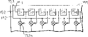
As mentioned above, when drive circuit is directly installed on the glass substrate with the COG method or monolithic when being formed on the glass substrate, if drive circuit is installed on the glass substrate, just inevitably not only will be to scan signal line and data signal line, also will to from external power to the power line of drive circuitry with to many holding wires 152 of drive circuit input clock signal, enabling signal, vision signal etc.. (seeing Figure 70) connects up.
Reference symbol S (S among Figure 70 herein
1, S
2...) shift-register circuit of expression sampled signal generation circuit 101, and the reference number 102a among Figure 70 ... the sampling switch of expression sample circuit 102.
If adopt used Ta or the TaN of conventional a-SiTFT-LCD
XAs the wiring material of power line and holding wire 152, the image quality difference of two ends about screen then, thus cause the problem that reduces display performance and so on.
This problem is that following two reasons cause jointly.
The one, if properties of materials is Ta or TaN
xThe electricalresistivity be 25-30 μ Ω cm and use with a kind of wiring material and connect up, if wiring width is that 100 μ m and thickness are 300nm, then the cloth line resistance is every centimetre 100 Ω.
Shown in Figure 71, another reason is each holding wire 152, as is used for (the S to shift-register circuit S
1, S
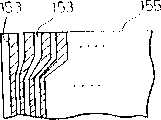
2...) input enabling signal the enabling signal line and be used for to sampling switch 102a ... the video signal cable of incoming video signal is connected, and is used for the connection welding 153 that is connected with the external circuit substrate and each input signal is formed one.The reference number 155 of Figure 71 is represented substrates herein.
Specific descriptions will illustrate the vision signal as holding wire 152.In diagonal was LCD about 25cm, when video signal cable is intersecting end-to-endly when continuous, its length of arrangement wire became and is about 20cm and the cloth line resistance of holding wire becomes 2k Ω.Moreover even in diagonal is LCD about 13cm, the cloth line resistance of holding wire becomes 1k Ω.When vision signal during via this high resistant signal wire transmits, impedance just increases.Shown in Figure 72, when a signal that has the A frequency band at connection welding 153 places as signal input part transmitted via holding wire 152, its frequency bandwidth characteristics such as A → B → C degenerated, at the end of holding wire 152, and signal band characteristic such as D.This phenomenon then causes the different trouble of two end image qualities about screen, can not the visual uniformly problem of display quality thereby cause.
In addition, if this phenomenon appears at enabling signal line 152 or is used for each shift-register circuit S (S to sampled signal generation circuit 101
1, S
2) input commencing signal clock cable 152, perhaps to shift-register circuit next step the transmission shift pulse circuit in, shown in Figure 73 (a)-73 (c), the waveform of the sampled signal of sample circuit 102 outputs changes from its early stage state, when signal was transmitted respectively going on foot of sampled signal generation circuit 101, it rose and the steepness of sloping portion diminishes.In other words waveform has taken place degenerates.That is, in the first step of sampled signal generation circuit 101 from shift-register circuit S
1The sampled signal of output with the representative of the waveform among Figure 73 (a), but shown in Figure 73 (b), goes on foot from shift-register circuit S at n
bWaveform b ' the representative of the sampled signal of output, this obtains owing to original waveform b degenerates.Further, shown in Figure 73 (c), represent with waveform c from the sampled signal of shift-register circuit S output in the m step, this obtains owing to original waveform c degenerates.Therefore sampling phase occurs and depart from its normal position and maybe can not produce the situation of sampled signal, thereby cause the problem of can not display quality good image.
The open No.398385/191992 (Tokukaihei 4-348385) of Japan Patent discloses a technology, and the voltage by means of detection flows to the electric current of display screen and control is added to display screen according to the magnitude of current comes the waveform of compensating signal data to degenerate.But the technology spy that this above-mentioned application discloses is used to the image diplay that adopts simple matrix to drive, and to adopt active matrix drive system be that the waveform that is caused by monolithic or COG (glass top chip) driver in the display of active device of the irregular operation of device circuitry degenerates and can not be used for for example having.
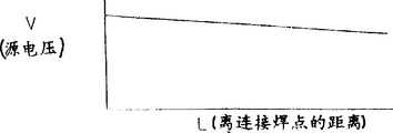
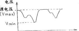
In addition, the increase of above-mentioned impedance (cloth line resistance) not only may occur in holding wire 152, and may occur in power line.Shown in Figure 74, when the distance to connection welding increased, source voltage descended.For example, even the source electric current is 1mA, when electric current flows through the power line of 2k Ω, the source voltage 2V that also descends.The decline of this source voltage causes irregular operation, comprises that each circuit that is connected in power line is not worked, signal level rises and falls or the like, thereby causes the decline of indicating characteristic.
When the size of screen in the LCDs became big, it is more obvious that the problems referred to above are certain to become.
Shown in Figure 75, increase in order to prevent wiring impedance, consider usually to increase holding wire 152 ' wiring width.At this moment, for example using wiring width with 100 μ m to change 10 times into is the way of 1mm, and the cloth line resistance can be restricted to about 1/10th.But in this method, for example if holding wire 152 ' impedance when further reducing, holding wire 152 ' just must be thicker.As a result, shown in Figure 76, when connection welding 153 ... be arranged at the periphery of substrate 155 so that when constituting with being connected of external circuit substrate, on the display no pixel area with respect to the area of pixel just with connecting up and the increase of connection welding area becomes big.In addition, appearance covers the shortcoming of signal leakage increase and so between electric capacity increase, the wiring according to the situation wiring.
In addition, increase, considered to use aluminium (Al) or aluminium alloy (Al-Si) as wiring material for preventing wiring impedance.For example, if come separated time as wiring material to use aforesaid wiring width and thickness with the Al-Si of electricalresistivity=5 μ Ω cm, then the cloth line resistance is limited to and is about the sixth that obtains with Ta or TaN.For example, as above-mentioned Al-Si when to be used for diagonal be image diplay about 25cm, total cloth line resistance becomes 330 Ω approximately, and when to be used for diagonal be image diplay about 13cm, becomes 170 Ω.At this moment, if consider loading condition (the source electric current is 1mA) same as described above, be used under the image diplay situation that diagonal is 25cm at wiring material, the voltage drop that is caused by wiring material can be limited in about 330mV.
But the source electric current wants the constant 1mA of remaining to be difficult to, so can occur in the somewhere of power line because the high-frequency source electrical current fluctuations that the on-off of each active device such as the transistor that is connected to power line causes and as any voltage waveform of high-frequency fluctuating of power line that Figure 77 is shown in.At this moment, if consider the signal data (Z of Figure 66 or Figure 68
1-Z
N) ratio that rises and falls to voltage fluctuation is 1: 1, then on screen in certain pixel, for example, the brightness meeting when voltage fluctuation is maximum is different from voltage fluctuation brightness hour very much.The impedance many more or power line of the active element number of on-off is high more, and this phenomenon is obvious more.
The influence of source voltage fluctuation discussed herein to signal data.Yet, the fluctuating of source voltage, that is the high frequency noise that produces in the power line is not only to signal data, and also also influential to other signal such as clock signal.Moreover high frequency noise not only causes the fluctuating of signal voltage level certainly, and causes such as other problems such as response time (speed of service) and circuit error runnings.
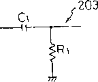
Shown in Figure 78, in routine techniques,,, for example on flexible substrate 163, a capacitor 165 has been installed in the outside of the demonstration substrate that is formed with pixel and power line 161 in order to limit high frequency noise, capacitor 164 is connected on the power line 161.Though this method can be used to reduce the high frequency noise that is created in demonstration substrate 155 outsides, be created in the high frequency noise that shows within the substrate 155 but be unsuitable for reducing, comprise the caused voltage fluctuation of electrical current fluctuations that causes according to each active device that is connected in power line 161 by on-off.
Top description list is understood the image diplay that has LCD.The problems referred to above, as cause the fluctuating of the signal level of the irregular operation of circuit, owing to signal waveform the degenerate signal delay that causes, the increase of high frequency noise, all with substrate on be equipped with circuit (comprise semiconductor active device and long electric lead, as be the power line of circuit supply, to the holding wire of circuit input signal) semiconductor device relevant.
The purpose of this invention is to provide a kind of being formed with comprises the semiconductor active device and is used for to being formed on the circuit supply on the substrate or the semiconductor device of the circuit of signal being provided, it can reduce the fluctuating of signal level, the delay of signal and the generation of high frequency noise, and can reduce the appearance than the irregular operation of bigger in the past circuit.
For finishing above-mentioned purpose, the feature of semiconductor device of the present invention is to comprise:
A substrate;
An active device circuit, it comprises a semiconductor active device, and the active device circuit has a plurality of inputs, and this active device is formed on the substrate;
One is used for carrying out the external connection terminal that is electrically connected with the external circuit on semiconductor device next door, and it is formed near the substrate edge; And
One is used for the conductor wire that is electrically connected between each input of active device circuit and external connection terminal, it is formed on the substrate,
Wherein conductor wire is that predetermined value or littler discrete line are formed by a plurality of cloth line resistances.
Use said structure, because conductor wire is divided into a plurality of lines, the length of conductor wire such as holding wire, power line has shortened, thereby might reduce its cloth line resistance.Therefore the fluctuating of may command signal level and the decline of source voltage.When semiconductor device was the image display device of LCD and so on, to obtain the method for even resistance, two edge graphs resembled the different situation of quality about screen with regard to not occurring by means of the cloth line resistance of adjusting each separated time.The result just can display quality image uniformly, thereby improve display characteristic.
In addition, for achieving the above object, the feature of another kind of semiconductor device of the present invention is to comprise:
A substrate;
An active device circuit that comprises the semiconductor active device, it is installed on the substrate;
One is transferred to the holding wire of active device circuit with baseband signal, and it gets two at least from the value of the outside input of semiconductor device on it, and holding wire is formed on the substrate; And
One is used for producing the waveform that waveform improves signal and improves signal generating circuit, and waveform improves signal and uses and add the waveform response signal component that degenerates to the baseband signal that passed holding wire and obtain so that waveform is improved the method that signal is added on the active device circuit.
Waveform wherein improves signal generating circuit following relationship:
(1)|v|<|V|;
(2) f≤F, wherein v is the peak swing that waveform improves the baseband signal component in the signal, and V comprises the degenerate peak swing of part of response signal component of waveform, and f is the frequency of baseband signal component and F is a waveform the degenerate frequency of response signal component.
Use said structure, because the peak swing v of baseband signal component and comprise that waveform degenerates relation between that part of peak swing V of response signal component by formula | v|<| V| represents, just might detect the waveform response signal component that degenerates from the baseband signal component.Moreover the relation because the frequency f of baseband signal component and waveform degenerate between the frequency F of response signal component represented by formula f≤F, just can be suitably to the baseband signal component setting waveform signal component that degenerates.
When the waveform that has produced in advance when the method for using improved signal and is added to the active device circuit, the waveform of baseband signal head end or tail end or head and the tail two ends degenerated with regard to Be Controlled.Its steepness has been maintained, thereby might prevent phase shift.In other words, the delay that passed the baseband signal of holding wire can prevent, and the error running of active device circuit also can be avoided.When semiconductor device was the image display device of LCD and so on, for example the time delay of sampling pulse can be prevented from, and desirable vision signal can be sampled under the time of rule, thereby may the good image of display quality.
In addition, for achieving the above object, the feature of another kind of semiconductor device of the present invention is to comprise:
A substrate;
An active device circuit that comprises the semiconductor active device, the active device circuit is formed on the substrate;
One outside the semiconductor device to the power line of active device circuit supply, power line is formed on the substrate;
An electric capacity that has reference potential forms electrode, and it will arrange to such an extent that make electrode have at least a part relative with power line; And
An electric capacity that is arranged between power line respect to one another and the electric capacity formation electrode forms dielectric.
Form an electric capacity with said structure, its electrode forms electrode by power line and electric capacity to be formed, and forms a capacitance-resistance filter by the equivalent resistance in the power line and be used as distributed constant circuit and capacitor, thus the impedance of reduction power line.Capacitance-resistance filter, promptly low pass filter then reduces the high frequency noise that produces in the power line, comprises the relevant caused voltage fluctuation of electrical current fluctuations of each semiconductor active device on-off that joins with power line.As a result, this structure can before more effectively reduce the irregular operation of active device circuit.
The present invention can be used for comprising the image display device such as LCD, but when the present invention was used to have the image display device of two substrates respect to one another, power line can be formed on the substrate and electric capacity forms electrode and can be formed on another substrate.For example, when the present invention was used for LCD, liquid crystal can be used as the electric capacity that is placed between power line and the electric capacity formation electrode and forms dielectric.And if show with liquid crystal and will form dielectric liquid crystal as electric capacity and separate with dividing plate, then planning to form dielectric liquid crystal as electric capacity can make a distinction with liquid crystal with demonstration.Therefore when selecting to form dielectric liquid crystal, do not require that it will be suitable for showing as electric capacity.Moreover under the situation that liquid crystal that is used to form electric capacity and the liquid crystal that is used to show separate with dividing plate, the liquid crystal that is used to show can be owing to using direct voltage to degenerate.
In addition, when the spacing between a pair of substrate seals with potted component in the semiconductor device, for example, liquid crystal is enclosed in LCD between the substrate, such as the image display device of plasma panel (wherein air seal is between substrate), the effective area ratio of display device can be by adopting electric capacity to form dielectric double as potted component and being improved.
Employing monolithic on substrate forms the method for active device circuitry, or adopt to form an active device circuit as semiconductor chip so that semiconductor chip is installed in method on the substrate, just can produce semiconductor device of the present invention.Be installed in COG under the first-class situation of substrate at semiconductor chip, the power line of powering to semiconductor chip is formed on the substrate, and is formed in the chip to the power line of semiconductor active device power supply.At this moment, by means of use with the semiconductor chip of above-mentioned similar methods on being installed on substrate in form capacitance-resistance filter, can reduce the high frequency noise in all substrates of semiconductor device.
In order to understand character of the present invention and advantage more fully, the detailed description of back is carried out with reference to the accompanying drawings.
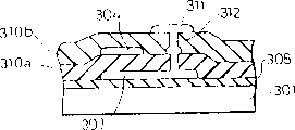
Fig. 1 is a key-drawing, shows the division state of video signal cable in the first embodiment of the invention LCD and the structure of the connection welding that separated time is connected in video signal cable;
Fig. 2 is the plane graph of substrate in the LCD, is formed with scan signal line, data signal line, scanner driver district, data driver district etc. on the substrate;
Fig. 3 is a line map, shows each line areas that is formed on the substrate;
Fig. 4 is the circuit diagram of shift-register circuit, and it forms one of circuit region that forms on the substrate;
Fig. 5 is a sequential chart, shows the sequential of input/output signal in the shift-register circuit;
Fig. 6 is the circuit diagram of buffer circuit, and it forms one of circuit that forms on the substrate;
Fig. 7 is a key-drawing, shows the separated time connection welding and is formed on connection status between the flexible substrate of edges of substrate;
Fig. 8 is a key-drawing, show be used for adjusting the vision signal separated time that is formed on the substrate impedance to obtain the arrangement of uniform impedance;
Fig. 9 is an oscillogram, shows the various waveforms of each circuit region in the LCD;
Figure 10 is a key-drawing, shows the vision signal separated time that is connected general connection welding;
Figure 11 is a key-drawing, shows another adjustment and is formed on the impedance of the vision signal separated time on the substrate to obtain the arrangement of uniform impedance;
Figure 12 is a key-drawing, shows another adjustment and is formed on the impedance of the vision signal separated time on the substrate to obtain the arrangement of uniform impedance;
Figure 13 is a key-drawing, shows the division state of Fig. 1 video signal cable in the another kind of wiring display packing;
Figure 14 is a key-drawing, shows the another kind arrangement of separated time connection welding;
Figure 15 is a key-drawing, shows the division state that is used in the second embodiment of the invention LCD to the enabling signal line of shift-register circuit input enabling signal;
Figure 16 is an oscillogram, shows the waveform of sampled signal in the LCD of Figure 15;
Figure 17 is a key-drawing, shows the division state of video signal cable enabling signal line and power line in the third embodiment of the invention LCD;
Figure 18 is a key-drawing, shows the formation state of separated time connection welding on the substrate;
Figure 19 is a key-drawing, shows in the LCD of Figure 17 the formation state of separated time connection welding on the substrate;
Figure 20 is a key-drawing, and the another kind that shows separated time connection welding on the substrate forms state;
Figure 21 is a key-drawing, shows another formation state of separated time connection welding on the substrate;
Figure 22 is a key-drawing, and the another kind that shows separated time connection welding on the substrate forms state;
Figure 23 is a key-drawing, shows another formation state of separated time connection welding on the substrate;
Figure 24 (a) and 24 (b) are key-drawings, and the another kind that shows separated time connection welding on the substrate forms state;
Figure 25 (a) and 25 (b) are key-drawings, show the structure of separated time connection welding; Figure 25 (c), 25 (d) and 25 (e) are key-drawings, show the structure that line is extracted from the separated time connection welding;
Figure 26 is a block diagram, shows the primary area structure of fourth embodiment of the invention LCD;
It is the oscillogram of source clock that Figure 27 (a)-27 (c) shows the waveform of various signals in the LCD: Figure 27 (a); Figure 27 (b) is the oscillogram that response improves signal; Figure 27 (c) is an oscillogram of improving clock signal;
Figure 28 is the circuit diagram of differential circuit shown in Figure 26;
Figure 29 is the circuit diagram of adder shown in Figure 26;
Figure 30 is the enlarged drawing of adder output signal waveform;
Figure 31 is a block diagram, shows the structure of drive circuit shown in Figure 26;
Figure 32 is a block diagram, shows a kind of structure that replaces response shown in Figure 26 to improve circuit;
Figure 33 (a)-33 (d) show another routine adder output improve clock signal: Figure 33 (a) show use to the source clock signal add a sine wave signal improve the method for signal in response and obtain improve clock signal; Figure 33 (b) show use to the source clock signal add the method for a pulse wave signal and obtain improve clock signal; Figure 33 (c) show use the position of departing to rise and fall district from the source clock signal add a response improve the method for signal and obtain improve clock signal; And Figure 33 (d) show a pulse of using the source clock signal add two responses improve the method for signal and obtain improve clock signal;
Figure 34 is a block diagram, shows the structure in fifth embodiment of the invention LCD primary area;
It is the oscillogram of source clock signal that Figure 35 (a)-35 (c) shows the waveform of various signals in the LCD: Figure 35 (a); Figure 35 (b) is the oscillogram of differential circuit input signal; And Figure 35 (c) is the oscillogram of differential circuit output signal;
Figure 36 is a block diagram, shows the structure shown in another illustration 34;
Figure 37 is a block diagram, shows the structure shown in the another illustration 34;
Figure 38 is a block diagram, shows the structure in sixth embodiment of the invention LCD primary area;
It is the oscillogram of source clock signal that Figure 39 (a)-39 (e) shows the waveform of various signals in the LCD: Figure 39 (a); Figure 39 (b) is the oscillogram of drive circuit input signal; Figure 39 (c) is the oscillogram that response improves signal; Figure 39 (d) is an oscillogram of improving clock signal; And Figure 39 (e) is the oscillogram that another response improves signal;
Figure 40 is a block diagram, shows the structure shown in another illustration 38;
Figure 41 is the vertical section schematic diagram in seventh embodiment of the invention LCD primary area;
Figure 42 is a key-drawing, shows basic conception of the present invention; Figure 43 is a key-drawing, shows the equivalent electric circuit of structure shown in Figure 42;
Figure 44 is a key-drawing, shows a basic structure example of semiconductor device;
Figure 45 is a key-drawing, shows another basic structure example of semiconductor device;
Figure 46 is a vertical section schematic diagram, shows the coupling part between the power line and another layer line in the semiconductor device;
Figure 47 is a floor map, shows the coupling part between the power line and another layer line in the semiconductor device;
Figure 48 is a floor map, shows a kind of change example of the coupling part between the power line and another layer line in the semiconductor device;
Figure 49 is a floor map, and the another kind that shows the coupling part between the power line and another layer line in the semiconductor device becomes example;
Figure 50 is a floor map, and another that shows the coupling part between the power line and another layer line in the semiconductor device becomes example;
Figure 51 is a longitudinal profile schematic diagram, shows a kind of change example of the coupling part between the power line and another layer line in the semiconductor device;
Figure 52 is a floor map, shows one that power line partly covers on the electric capacity formation electrode in the semiconductor device and becomes example;
Figure 53 is a longitudinal profile schematic diagram, shows electric capacity in the semiconductor device and forms electrode and be formed on from substrate than becoming example from more nearby one of power line;
Figure 54 is a longitudinal profile schematic diagram, shows the change example that power line connects up on two layers in the semiconductor device;
Figure 55 is a floor map, and another that shows that power line in the semiconductor device covers partly that electric capacity forms electrode becomes example;
Figure 56 is a longitudinal profile schematic diagram, shows the structure in eighth embodiment of the invention LCD primary area;
Figure 57 is a key-drawing, shows the equivalent electric circuit of structure shown in Figure 56;
Figure 58 is a longitudinal profile schematic diagram, shows a change example having omitted the diaphragm that covers power line and electric capacity formation electrode in the LCD;
Figure 59 is a longitudinal profile schematic diagram, shows power line in the LCD or electric capacity and forms electrode and have double-deck of being made up of ITO (indium tin oxide) film and golden tunic to become routine;
Figure 60 is a longitudinal profile schematic diagram, shows power line in the LCD or electric capacity and forms electrode and become routine by double-deck another of being made up of ITO film and metal film;
Figure 61 is a longitudinal profile schematic diagram, shows electric capacity in the LCD and forms electrode and also become example with one that does electrode;
Figure 62 is a longitudinal profile schematic diagram, shows in the LCD to show with liquid crystal and to form of separating with dividing plate between dielectric liquid crystal as electric capacity and become routine;
Figure 63 is a longitudinal profile schematic diagram, shows electric capacity in the LCD and forms dielectric and also become example as one of potted component;
Figure 64 is a key-drawing, shows that semiconductor chip is installed in the change example that is formed with the pixel place on the substrate in the LCD,
Figure 65 is a key-drawing, shows the wiring example of the power line that is formed on the substrate;
Figure 66 is a block diagram, shows the structure that adopts the data driver of progressive-scan system in the conventional LCD;
Figure 67 is the sequential chart of various signals in the data driver shown in a Figure 66;
Figure 68 is a block diagram, shows the structure that adopts the data driver of point by point scanning system in the conventional LCD;
Figure 69 is the sequential chart of various signals in the data driver shown in Figure 68;
Figure 70 is a key-drawing, shows the structure in data driver primary area in the conventional LCD;
Figure 71 is a key-drawing, shows enabling signal line in the conventional LCD and is used for cloth line states to the video signal cable of shift-register circuit input signal;
Figure 72 shows signal band characteristic in the drive circuit in the conventional LCD with the variation by distance;
It is the oscillogram of source signal that Figure 73 (a)-73 (c) shows the wave form varies of sampled signal in the conventional LCD: Figure 73 (a); Figure 73 (b) oscillogram shows the situation that waveform degenerates that takes place; And Figure 73 (c) oscillogram shows the situation that a waveform worsens;
Figure 74 is a key-drawing, shows the variation of power line voltage in the conventional LCD;
Figure 75 is a key-drawing, shows a kind of structure that video signal cable is done thickly in the conventional LCD;
Figure 76 is a key-drawing, shows in the conventional LCD structure of connection welding on the edges of substrate;
Figure 77 is a key-drawing, shows in the conventional LCD voltage waveform of certain part in the power line;
Figure 78 is a key-drawing, has explained a kind of conventional method that reduces high frequency noise, and wherein capacitor is installed in demonstration substrate outside and is connected on the power line.
First embodiment
With reference to Fig. 1-14, below the first embodiment of the present invention will be discussed.
Present embodiment will illustrate and adopt the display of the inventive method to the sample circuit incoming video signal of data driver on a kind of active matrix type liquid crystal display that adopts the driver monolithic system as image diplay, particularly video signal cable.
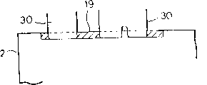
LCD has a LCDs of being made up of a pair of substrate, and as shown in Figure 2, scan signal line 3 ..., data signal line 4 ..., with adopting the scanner driver 5 of driven sweep holding wire 3 and being used for the data driver 6 of driving data holding wire 4, all be installed on the substrate 2 in a pair of substrate.Scan signal line 3 ... with data signal line 4 ... intersect each other, and thin-film transistor (TFT) 16 (it is the pixel driving element) and pixel capacitors 15 (wherein the supply of electric charge is subjected to the control of TFT16) are formed near the (see figure 3) of each intersection point.Pixel capacitors 15 ... with another substrate together, nationality helps liquid crystal is contained in the gap and forms pixel (not drawing).A lot of pixels are arranged to form matrix and constitute a pixel region 7.Utilize the voltage that produces between the respective electrode, pixel is used to control the light emission state of liquid crystal with displayed image.
As shown in Figure 3, the data driver that is installed on the substrate 2 mainly is made up of four circuit regions: a sampled signal generation circuit region 8; A sample circuit district 9; A change-over circuit district 10; And buffer circuit district 11.
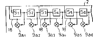
Sampled signal generation circuit region 8 comprises a shift-register circuit district 8a and many buffer circuit 8b ...As shown in Figure 4, shift-register circuit district 8a is by many shift-register circuit S (S
1, S
2) form, wherein import enabling signal and export sampled signal (with the pulse signal of predetermined interval input) in case sample circuit district 9 one after the other to sample video.The sequential of input and output is shown in Fig. 5.As shown in Figure 6, buffer circuit 86 ... the sample circuit district 9 that forms and need drive megacryst pipe yardstick by many phase inverters according to the output signal of the shift-register circuit district 8a of small transistor yardstick.Near more from the output area, the transistorized size of phase inverter is fixed greatly more.
As shown in Figure 3, sample circuit district 9 comprises many sampling switch 9a ... with sampling capacitor 9b ... be used for to sample video.Sampling switch 9a ... be used for the information stores of vision signal is arrived corresponding sampling capacitor device 9b ... in, and each on-off operation of sampling switch is all controlled according to the sampled signal of sampled signal generation circuit 8 outputs.
Change-over circuit district 10 comprises change over switch 10a ... with maintenance electric capacity 10b, and the information that is stored among the sampling capacitor device 9b is switched to maintenance capacitor 10b according to the switching signal that will import ...
Here describe in detail with reference to Fig. 1,7 and 8 and be used for a plurality of sampling switch 9a in sample circuit district 9 ... the structure of the cloth line states of the video signal cable of incoming video signal, connection welding 19 (be used for connecting terminal), be used for be formed on substrate edge on the separated time that is connected of flexible substrate (external circuit substrate) etc.
As shown in Figure 1, the sampling switch 9a in the sample circuit district 9 ... be divided into N group (every group of two switches), for example (9a
1And 9a
2), (9a
3And 9a
4) ...Vision signal separated time 18 ... then be connected to corresponding group.One end of each vision signal separated time 18 is connected to a connection welding 19 (being used for being connected with flexible substrate for the separated time that is formed on the edges of substrate).Conventional video line is divided and forms N video separated time 18 ..., so that shorten the length of video line and reduce the cloth line resistance.For example, if N is 10, its cloth line resistance of the holding wire of the 2k Ω that has pointed out in background of the present invention can be reduced to about 20 Ω.
As a result, the reduction of cloth line resistance can limit the increase of vision signal line impedence.If video signal cable is divided into the N section, than conventional video signal cable, the increase of impedance can be restricted to about 1/N, thus the acquisition Low ESR.Point out that in passing the number of number of partitions N and every group of sampling switch 9a is random and suitable the setting.
Simultaneously, each video signal cable 18 ... connection welding 19 settle along the edge of substrate 2., and representing with v that then connection welding is decided to be and satisfies formula h>v if the terminal of solder joint 19 represents with h at the width that is parallel on the direction of substrate edge perpendicular to the width on the direction of substrate edge.This permission connection welding 19 becomes the rectangle solder joint with the substrate edge arranged parallel, thereby obtains with the large contact surface of flexible substrate long-pending.As a result, promptly use video signal cable to be divided into a plurality of structures, video signal cable still can keep low impedance and can not use the connection reliability of flexible substrate to degenerate.Herein, the connection between connection welding 19 and the flexible substrate 30 not necessarily will cover whole solder joint, as shown in Figure 7, can make partly connection.
Yet, when being connected in corresponding video signal separated time 18 ... corresponding sampling switch 9a ... the impedance fluctuating in the zone of input at each vision signal separated time 18 ... in when all big, even formed the vision signal separated time for the impedance that reduces video signal cable, also the circuit error running may take place.Under the vision signal situation, can be used as the method that suppresses inhomogeneous show state within the specific limits, or the like, be limited in the signal level fluctuating near the pixel place ± 1/32 or littler, therefore wish basically in connection welding 19 to each sampling switch 9a ... scope in restriction impedance fluctuating δ R<± 3.1%.
Therefore, in the present embodiment, as shown in Figure 8, along with node q and the q ' of the main signal line 18a of vision signal separated time 18 becomes farther from connection welding 19, at node q, q ' ... the signal branch line district 18a ' of place branch, 18a ' ... live width become big.That is, when holding wire from connection welding 19 farther place branches the time, the cloth line resistance is lowlyer fixed, thereby makes from connection welding 19 to each sampling switch 9a ... the zone in impedance even so that the variation of control group.Herein, when sampling switch 9a was divided into more than three or three one group, the structure of vision signal separated time 18 was pointed out by the dotted line among the figure.At this moment, much more farther that node q " locates to form signal branch line 18a ', makes it have bigger width than the signal branch line 18a that locates branch at node q ' from connection welding 19 than node q and q '.
Then, the operation that has the data driver 6 of said structure with reference to the oscillogram discussion of Fig. 9.Herein, k among the figure and m represent to be connected on " k " line and " m " line the signal in each circuit region of data driver 6 of data wire 4, and K and L represent to be connected on " K " line and " L " line the signal in each circuit region of scanner driver 5 of scan signal line 3.
Sampled signal is one after the other exported from sampled signal generation circuit region 8, when sampled signal place " H " attitude, and corresponding sampling switch 9a ... connected in succession, the information of vision signal is stored in corresponding sampling capacitor device 9b ... in.At this moment, because vision signal is via corresponding video signals separated time 18 ... and import, it is stored in sampling capacitor device 9b ... in and do not change its frequency bandwidth characteristics.And this moment, corresponding transmitting switch 10a was turned off.Afterwards, after scheduled sampling time is gone over, sampled signal place " L " attitude.As a result, sampling switch 9a ... turn-offed in succession again.After all data signal lines 4 are all sampled, when being input to change over switch 10a ... transmission signals place " H " attitude the time, change over switch 10a is connected simultaneously, so that is stored in corresponding sampling capacitor device 9b ... in information be transferred to corresponding maintenance capacitor 10b.Afterwards, after predetermined migration period is gone over, switching signal place " L " attitude, corresponding change over switch 10a is turned off again simultaneously.
As a result, in a horizontal cycle, the information that is stored among the corresponding maintenance capacitor 10b just outputs to corresponding data signal line 4 via buffer circuit district 11.
From the sweep signal (gating signal) of scanner driver 5 output then almost with transmission signals " H " attitude simultaneously, TFT16 is connected.As a result, data are written into pixel so that shown with the good image quality with non-homogeneous show state not.
As mentioned above, in LCD of the present invention, owing to the sampling switch 9a that is used in sample circuit district 9 (it is the built-up circuit of data driver 6) ... the video signal cable of incoming video signal by repeated segmentation to form vision signal separated time 18 ... (the one end is connected to connection welding 19), it is shorter than conventional line that the length of video signal cable just becomes, and signal is input to corresponding sampling switch 9a by the short signal line ...This has just limited the increase of vision signal line impedence, thereby reduces impedance.As a result, the frequency bandwidth characteristics of the vision signal by video signal cable is almost constant, and therefore two edge graphs resemble qualitative difference about not occurring on the screen, thereby obtains to show uniformly.
In addition, in the present embodiment, vision signal separated time 18 connects connection welding 19 on it and is configured to make along the end points width h that is parallel to the substrate edge direction greater than along (h>v) is so become greatly with the contact area of flexible substrate 30 perpendicular to the end points width v of substrate edge direction.Therefore, even in order to reduce impedance, video signal cable is by repeated segmentation, and thereby the interface number with flexible substrate 30 is increased, connection reliability does not degenerate yet.That is, as shown in figure 10, only use a kind of video line by the structure of repeated segmentation, for example increase and cut apart number in order to obtain Low ESR, the connection welding number of discrete installation just increases, and also increases with the interface number of flexible substrate 30.As a result, connection reliability degenerates, and adopt the advantage of driver monolithic system also to lose, but this problem can not appear in above-mentioned structure.
And, in the present embodiment, along with the node q among the main signal line district 18a of vision signal separated time 18 and q ' (signal branch line district 18a ' 10a ' is branched at this) when connection welding 19 becomes farther, it is big that the live width of signal branch line 18a ' 18a ' becomes.As a result, from connection welding 19 to corresponding sampling switch 9a ... impedance in the zone keeps constant and variation impedance is controlled.This just can suppress since from connection welding 19 to corresponding sampling switch 9a ... signal line impedance changes the circuit error running that causes in the zone, thereby obtains higher display characteristic.
Here, for reaching this purpose, except that the method for present embodiment, for example, as shown in figure 11, main signal line district 18a can form along with holding wire district 18a becomes far away and its width is become big from connection welding 19, and this just need not change the signal branch line district 18a ' that is branched ... live width.Moreover, as shown in figure 12, the length of vision signal separated time 18 can be made equally longly, make the line length difference be about δ R<± 3.1%.In addition, the thickness of each video signal cable 18 also can change, and these methods will according to circumstances adopt.Each video signal cable 18 ... structure be not limited to shown in the figure, as shown in Figure 8, part shows sampling switch 9a shown in the dotted line ... the structure of vision signal separated time 18 when being divided into triplets.
In addition, the signal input part that is connected in connection welding 19 shown in Fig. 1 is with the distance between each sampling switch 9a (for example video signal cable node d and sampling switch 9a
1Between distance) be different from node d and sampling switch 9a
2Between distance, but this be for the ease of the performance wiring diagram.As shown in figure 13, video signal cable node d ' and sampling switch 9a
1Between distance equal node d ' and sampling switch 9a
2Between distance, in other words, the present invention arranges to such an extent that make node d ' and sampling switch 9a
1Between impedance equal node d ' and sampling switch 9a
2Between impedance.
In addition, in the present embodiment, connection welding 19 is to form along the edge of substrate 2, but is not limited to this method, for example as shown in figure 14, can settle many connection welding 19 '.The connection welding 19 of settling along edges of substrate can cause can't be input to another signal the mistake etc. that solder joint forms the district, or when the solder joint area is big because be heated and cool off after solder joint expand or contraction occurs breaking etc.Yet, settle solder joint to address this problem with the method for cutting apart.At this moment, with the interface number increase of outside, but, provide big contact area, thereby prevented that connection reliability from degenerating unlike structure shown in Figure 10.
Present embodiment has illustrated the structure that video signal cable is cut apart, but the invention is not restricted to this, and for example, another kind of holding wire or power line also can be cut apart.And this method not only can be used for input signal cable, and can be used for output signal line.
Moreover, present embodiment has illustrated image display device (particularly LCD), but the invention is not restricted to image diplay, be applicable to that also active device circuit (comprising active of semiconductor) and the long line of conduction (as be used for to the power line of active device circuit supply, be used for holding wire to the active device circuit input signal) are formed on any semiconductor device on the substrate.
As mentioned above, a kind of semiconductor device, it comprises:
A substrate;
An active device circuit that comprises a semiconductor active device, the active device circuit is formed on the substrate and has a plurality of inputs;
One is used for the outside link that is electrically connected with the external circuit outside the semiconductor device, and it is formed near the edges of substrate; And
One is used for forming the conductor wire that is electrically connected between each input of active device circuit and outside link, and it is formed on the substrate,
Electric lead wherein gets predetermined value by many cloth line resistances or littler separated time is formed.
Adopt this structure, owing to shorten such as the conductor wire of holding wire, power line, the cloth line resistance can be lowered, thus the fluctuating of possible control signal level and the decline of source voltage.As a result, when semiconductor device was a image display device such as LCD, its display characteristic can be enhanced.
Be arranged to link according to the present embodiment semiconductor device of said structure and form along edges of substrate, and along the end width that is parallel to the edges of substrate direction greater than along end width perpendicular to the edges of substrate direction.
Use this structure, though the conductor wire such as holding wire, power line by repeated segmentation, the connection reliability between device and the external circuit substrate does not reduce yet.
In said structure, the formation that semiconductor device (image display device) is arranged to each separated time makes outside link drop in the scope of cloth line resistance mean value ± 3.1% to the wiring changes in resistance between the active device circuit input area.In this way, when the cloth line resistance of adjusting each line falls into above-mentioned scope, do not observe irregular demonstration, thereby improve display characteristic.
Followingly clock cable will be discussed or be used for enabling signal is input to shift-register circuit S as second embodiment ... the structure of enabling signal line.
Second embodiment
Below with reference to Figure 15 and Figure 16 the second embodiment of the present invention is discussed.
Here for ease of explaining, with aforementioned first embodiment element of same structure and function is arranged and the element described all shows with identical reference number, and omit description of them.
LCD as the present embodiment of image diplay, as shown in figure 15, though video signal cable is cut apart in the aforementioned embodiment, but video signal cable is settled with conventional method, and clock cable or be used for to shift-register circuit S ... the enabling signal line of input enabling signal is split into clock signal separated time 20 ... or enabling signal separated time 20 ...Each clock signal separated time 20 herein ... or an end (not drawing) of each enabling signal line 20 is connected to connection welding 19.
Use this method, when clock holding wire or enabling signal line are arranged with split plot design, as shown in figure 16, even for the n step shift register circuit S away from signal input part
nWith m step shift-register circuit S
m, also can approach original waveform b and c by the respective waveforms of b " and c " representative.Under the situation that the enabling signal line is cut apart according to the structure of drive circuit, should adjust the phase place of starting impulse herein, to each parallel circuit.
As a result, phase change in sampled signal, do not occur, thereby improve display characteristic.
The 3rd embodiment
Followingly explain the third embodiment of the present invention with reference to Figure 17-25.
For ease of explaining, show with identical reference number with previous embodiment 26S Proteasome Structure and Function components identical and the element described, and omit their description.
In the LCD (image diplay) of present embodiment, as shown in figure 17, enabling signal line (or clock cable), video signal cable and power line by repeated segmentation to form enabling signal separated time (or clock signal separated time) 20 ..., vision signal separated time 18 ... with power supply separated time 21 ...
Under the situation that forms many wirings, as shown in figure 18, corresponding signal lines 20 ..., 18 ... with 21 ..., and the connection welding 19 that is used for power line ... can be arranged to crisscross along substrate 2 edges.As shown in figure 19, except that a line that will be placed in the inner edge of substrate, corresponding welding spots is to be arranged to from edges of substrate to become delegation via contact hole to the direction of each substrate interior but in the present embodiment.But contact hole can be used for being placed in a line of the inner edge of substrate.This method makes to divide to count out in Figure 18 structure and can not be increased to more than certain number, and has eliminated such as homologous lines on the substrate 20 ..., 18 ..., 21 ... defect with power line wiring complexity and so on.
In addition, not only can adopt this structure, and can adopt Figure 20 for example with shown in 21 via being connected the structure that branch solder joint 19 connects up, or the combination of these structures.
In all holding wires and power line, do not need to reduce under the situation of impedance, can adopt normal connection welding 2020 to be placed in structure (as shown in figure 22) between the rectangle connection welding 1919 that impedance reduced, to have a normal connection welding 20 of narrow width with narrow width ... be placed in the structure (as shown in figure 23) that reduced within the connection welding 19 that resistance holds, with the combination of Figure 23 opposite configuration or these structures.
The adjacent connection welding 1919 of separated time not necessarily will be used for same class holding wire.For example shown in Figure 24 (a), the connection welding E of enabling signal line and the connection welding G of power line can be arranged to the connection welding F that is adjacent to the enabling signal line.And, in a plurality of connection welding 19 ... be arranged under the situation of a plurality of row along edges of substrate, connection welding 1919 not necessarily will be arranged to connection welding E and F each justified margin of going in two row shown in Figure 24 (a), and each row does not line up in two row so connection welding 1919 can be arranged to.
And, each tie point 19 ... 20 ... layer in substrate is not limited to above-mentioned from 1 to 3 layer, can adopt the layer more than three layers.Solder joint sum everywhere should be always inconstant, so the layout of solder joint also is random.Moreover, be placed in the connection of each holding wire in the substrate and separately be random, and be positioned at the corresponding connection welding 19 of substrate perimeter ... 20 ... can contact or leave edges of substrate with edges of substrate.
The structure of connection welding 19 can be angie type or the round formula shown in Figure 25 (b) shown in Figure 25 (a).Moreover each vision signal separated time also is random from the wire structures of connection welding 19; Angie type shown in Figure 25 (c), the circle formula shown in Figure 25 (d), trapezoidal formula shown in Figure 25 (e), or the like.
As mentioned above, be arranged to a plurality of links according to the semiconductor device of present embodiment and be present on the substrate, and in the delegation on the direction of a plurality of link in being arranged in from the edges of substrate to the substrate.This just might utilize area limited on the edges of substrate well and increase holding wire or power line cut apart number.At this moment, signal separated time or power line just can not be disorderly and unsystematic.
The driver portion of LCD has been described, but the circuit of indication is not limited to driver portion in first to the 3rd embodiment, and image diplay is not limited to LCD.Therefore also can adopt other circuit and display, for example adopt the circuit of handling the stylus input signal as circuit part with adopt that plasma shows, EL (electroluminescence) shows etc. as display.
The 4th embodiment
Followingly the fourth embodiment of the present invention is discussed with reference to Figure 26-40.Present embodiment is also discussed the image display device as the example of this semiconductor device.
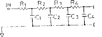
LCD as the present embodiment of image diplay adopts active matric point by point scanning system and comprises active element.In this LCD, be formed on a circuit arrangement on the substrate with image displaying area and work to be used for driving image displaying area as a drive circuit.As shown in figure 26, LCD had a response to improve circuit 202 (waveform improves signal generating circuit) (not drawing) before the drive circuit 201 that drives LCDs.
Response improves circuit 202 and comprises that one is used for that the degenerate response of response signal component improves the differential circuit 203 of signal (shown in Figure 27 (b)) as waveform from producing as the source CLP of pulsed baseband signal component shown in Figure 27 (a), with one be used for that response is improved signal and be added to source CLP, in other words, response is improved signal mix with source CLP to produce one and improve clock signal (hereinafter referred to as improving CLP) is improved signal (shown in Figure 27 (c)) as waveform adder 204 with adopting.Differential circuit 203 is by a resistance R for example shown in Figure 28
1With a capacitor C
1Form.As everyone knows, the pulsewidth t that improves signal from the response of differential circuit shown in Figure 28 (b) output is by R
1And C
1(the t=R that decides of product
1C
1), that is the time constant of differential circuit 203.
With regard to the waveform that prevents to improve CLP degenerates, the installation site that response improves circuit 202 is comparatively suitable near drive circuit 201, does not improve circuit 202 and is installed in the certain limit between clock generating circuit 206 and the drive circuit 201 but also do not limit to respond.
As shown in figure 29, adder 204 is by for example operational amplifier OP
1, four resistance R
2With a resistance R
3Form.Here resistance R
3R is arranged
3=R
2/ 2 relation.In this circuit, if operational amplifier OP
1The input voltage of inverting input show with V
-, non-inverting input input voltage show with V
+, input a and b input voltage show with V respectively
aAnd V
b, and the output voltage of output c shows with V
c, following relationship: V is then arranged
+=(R
2/ 3) (V
a/ R
2+ V
b/ R
2)=(V
a+ V
b)/3V
-={ V
c/ (R
2/ 2+R
2) R
2/ 2=V
c/ 3V
+=V
-Therefore, V
c=V
a+ V
bAdder is only limited to this example herein, and it can have other structure.
Improve CLP and have the baseband signal component S shown in the thick line among Figure 30
s, it gets the overshoot component S that high/low (1/0) is worth, is added on source CLP rise and fall side
oWith down towards component S
u(fine rule indication).
The drive circuit 201 (data driver) that has structure shown in Figure 31 comprises a shift register 211 and a sample circuit 212.Drive circuit 201 is installed on the glass substrate that is formed with the LCDs pixel region.Improve CLP and starting impulse (hereinafter referred to as STP) and be imported into shift register 211.
As mentioned above, just be input to the improving with regard to the CLP of shift register 211 shown in Figure 27 (c), it rises owing to cloth line resistance and parasitic capacitance in the drive circuit 201 slow down (distortion).But because overshoot component S
oBe added in advance and improved CLP, so the waveform that can avoid improving CLP degenerates, and the delay of rising is difficult to occur.And, if the influence of parasitic capacitance is big, then correspondingly submit to the ratio of overshoot component just can eliminate the delay of rising.
If the output number of driver is N, then STP (it starts the data sampling of a horizontal scanning period) is transfused to so that according to the time of improving CLP each output area output sampling pulse C from shift register 211
1-C
NThe sampling pulse C that vision signal is exported by shift register 211 in sample circuit 212
1-C
NSampling, and the signal that sampling obtains is transferred to data signal line immediately.
Utilization reportedly is passed to data signal line according to logarithm sequential is added on the method for scan signal line with scanning impulse from scanner driver, and the data of a horizontal scanning period are added on the predetermined pixel of LCDs.This makes LCD can show high-quality image.
In the present embodiment, improve CLP herein overshoot component S is arranged ahead of the curve
oAnd have down towards component S on the edge, back
uBut because 211 in shift register is just carried out shifting function when improving the CLP rising, so the back is following to component S along what locate
uBe unwanted.On the contrary, if shift register 211 is carried out shifting function when improving CLP decline, then only need the following of place, edge, back towards component S
u
In addition, in the present embodiment, response improves signal and is added to response and improves in the circuit 202 from the source CLP of clock generating circuit output, but response improves signal adds improving CLP and can be output thereon from clock generating circuit 206, in other words, clock generating circuit 206 can comprise that response improves circuit 202.
Moreover, shown in figure 32, improve CLP in order to produce, becoming the source CLP that improves CLP according to differential can produce in clock generating circuit 206, and can be handled in differential circuit 203.
Improve CLP in order to produce, the differential signal that improves signal in response is added to forward position and the edge, back of source CLP, but the synchronous response of another and source CLP improves signal, the response with sine wave shown in Figure 33 (a) improves the pulse type response shown in signal or Figure 33 (b) and improves signal, also can add.And, improve signal in response, have triangular wave or the trapezoidal wave person also can add.Response improves forward position and the edge, back that signal not only can add to source CLP, also can add to the place (shown in Figure 33 (c)) of slightly relatively rising and sloping portion.Moreover, with regard to improving CLP, shown in Figure 33 (d), ahead of the curve and the back along between can add two responses and improve signal.Herein if produce harmful consequence, that is the improvement of rising characteristic has influence on falling characteristic, or opposite, and the improvement of falling characteristic influences rising characteristic, then wishing to respond the position of improving the signal insertion is between CLP forward position, source and the edge, back, in other words is before two/a bit.
Consider above-mentioned situation, improve signal such as the waveform that improves CLP and should satisfy following requirement: as shown in figure 30, if being equivalent to source CLP and being the peak swing that the peak swing of baseband signal component shows the part that with v baseband signal characteristic has been enhanced shows with V, following relation is then arranged: | v|<| V| is if the frequency of baseband signal component shows that responding the frequency of improving signal with f shows that with F following relation is then arranged:
f≤F
In other words, when relation | v|<| when V| sets up, response improve signal concerning the CLP of source can be one can detected component.And when Equation f≤F set up, response improved signal and can add to source CLP suitably.
In addition, because differential circuit 203 simple structures utilize differential circuit just can simplify the structure of circuit.Structure shown in Figure 26 is improved slightly than structure shown in Figure 32.But because response improves signal is to be produced and added to source CLP by differential circuit 203 to improve CLP with generation, improves signal so can more suitably form response.
As mentioned above, the active element that many carrier mobilities are high is used in the LCD, is 5cm as the carrier mobility μ of active element
2/ Vsec or higher (μ 〉=5cm
2/ Vsec) polycrystalline SiTFT (hereinafter referred to as p-SiTFT) is used to LCD, and drive circuit 201 monolithics are formed on the glass substrate that constitutes the liquid crystal display screen.
In the structure of present embodiment, improve CLP and be with respond and improve the method generation that signal adds to source CLP, but this structure also can be used for for example can obtaining starting impulse, another data-signal of (1/0) two value of H/L and can obtain many gray scales vision signal of (that is as improving the many-valued of CLP).Also can be used for other embodiment that the back will be mentioned.
As mentioned above, the semiconductor device of present embodiment is arranged to and comprises:
A substrate;
An active device circuit that comprises a semiconductor active device, this active device circuit is formed on the substrate;
A holding wire that is used for baseband signal (it gets two values from semiconductor device outside input at least) is transferred to the active device circuit, this holding wire is formed on the substrate; And
One is used for producing waveform that waveform improves signal and improves signal generating circuit (waveform improve signal use add the degenerate method of response signal component of a waveform to the baseband signal by signal wire transmits and obtain) and be added on the active device circuit so that waveform is improved signal
Wherein waveform improves signal generating circuit following relationship:
(1) | v|<| V|; And
(2) f≤F, wherein v is the peak swing that waveform improves baseband signal component in the signal, and V comprises the degenerate peak swing of response signal component of waveform, and f is the frequency of baseband signal component, and F is a waveform the degenerate frequency of response signal component.
Use this structure, can prevent delay, thereby avoid the error running of active device circuit by the baseband signal of signal wire transmits.At semiconductor device is under a kind of situation of the image display device such as LCD, can prevent for example time delay of sampling pulse, thereby might take a sample to desirable vision signal at official hour.The result just can show high-quality image.
Moreover the feature of the semiconductor device of present embodiment is: waveform improves signal generating circuit and is one and is used for the baseband signal of input is from the outside carried out differential so that produce the differential circuit that waveform improves signal.This can make designs simplification.
And the feature of the semiconductor device of present embodiment is: waveform improves signal generating circuit and comprises:
Be used for taking place the waveform waveform of the response signal response signal generating means that degenerates that degenerates; And
Be used for waveform waveform that the response signal generating means the takes place response signal that degenerates that degenerates is added to the adder that the baseband signal of input from the outside gets on.This is can be suitably independent to produce degenerate response signal and desirable waveform of waveform and improves signal.At semiconductor device is under a kind of situation of image display device, and for example vision signal can be suitably sampled, thereby might show high-quality image.
The 5th embodiment
Explain the fifth embodiment of the present invention below with reference to Figure 34-37.
For ease of explaining, with aforementioned the 4th embodiment same structure and function are arranged and those elements of having described show with identical reference number and omit description of them.
As shown in figure 34, drive circuit 201 (data driver) is formed on the glass substrate that constitutes the liquid crystal display screen.Drive circuit 201 comprises the differential circuit 203 that improves circuit as phase characteristic.Differential circuit 203 is formed on all primes of N level place shift register 2011.
Use said structure, with regard to regard to the source CLP of clock generating circuit (not drawing) output, because forward position and edge, back are owing to cloth line resistance or parasitic capacitance in the drive circuit 1 slow down, waveform is deformed into the waveform shown in Figure 35 (b) shown in Figure 35 (a).In other words, the source CLP that waveform degenerates taking place is imported into differential circuit 203.Shown in Figure 35 (c), its forward position of the waveform of source CLP and back are along all steep.As a result, can compensate and rise and fall delay, so that LCD can show high-quality image.
Use said structure, differential circuit 203 is placed on all primes of N level shift register 211, but as shown in figure 36, differential circuit 203 can be placed in the previous stage place that the level of branch takes place the CLP feeder line according to the shift register 211 at N level place.Moreover, as shown in figure 37,, can improve response with the method for handling the transmission pulse itself that is transmitting to shift register 211 later stages of differential circuit 203 (that is to).
The semiconductor device of present embodiment is arranged to and comprises:
A substrate;
An active device circuit that comprises a semiconductor active device, this active device circuit is formed on the substrate; And
A holding wire that is used for transmitting from the input signal of semiconductor device outside input to the active device circuit, this holding wire is formed on the substrate;
Wherein the active device circuit comprises that a phase property that is used for phase property in the compensating signal component (it becomes the indication of the stale circuit operation that causes owing to waveform degenerates with respect to input signal) improves circuit.In other words the structure of the 4th embodiment that compares, is used for preventing that waveform from degenerating causes that the waveform that the degenerates response signal component that degenerates adds to input signal in advance, and this structure is easier to prevent degenerating of input signal.
In addition, the feature of the semiconductor device of present embodiment is: it is a kind of differential circuit that phase property improves circuit.This can simplify circuit structure.
The 6th embodiment
Followingly explain the sixth embodiment of the present invention with reference to Figure 38-40.
For ease of explaining, with previous embodiment same structure and function are arranged and those elements of having described show with identical reference number and omit description of them.
As shown in figure 38, LCD comprises that one of shift register 211 all prime places, N level place in the drive circuit 201 (data driver) is improved signal and inserts circuit 231.Improve signal and insert circuit 231 as being equivalent to signal component that waveform degenerates and improving signal (shown in Figure 39 (c)) and be imported into from the source CLP of clock generating circuit (not drawing) output from the response that improves signal generating circuit 232 outputs.Improve signal generating circuit 232 and improve signal and insert circuit 231 and form waveforms and improve circuit.Improve signal and insert circuit 231 and comprise adder for example shown in Figure 29 204, and will respond and improve signal and add to source CLP so that it is outputed to shift register 211.
Use said structure, because the waveform that the rising that cloth line resistance and parasitic capacitance cause the drive circuit 201 and the district that descends take place degenerates and is deformed into after the waveform shown in Figure 39 (b), source CLP is imported into and improves signal and insert circuit 231 from the waveform (shown in Figure 39 (a)) of the source CLP of clock generating circuit output.In improving signal insertion circuit 231, improve signal from the response shown in the Figure 39 (c) that improves signal generating circuit 232 inputs and be added to input signal so that produce the CLP that improves shown in Figure 39 (d).Improve CLP and then be output to shift register 211.The rising and the decline district that improve CLP are very steep, thereby improve the response in the shift register 211.
If the pulse duration that response improves signal is shown the running frequency that is formed on the drive circuit 201 on the glass substrate with T and is shown with f, then pulsewidth T should set like this, make to obtain following relation: T<1/f therefore, for example the differential signal of source CLP shown in Figure 39 (e) also is used as response and improves signal.In other words, signal is as long as can improve the CLP forward position and the steepness on edge, back, and it just can be used as response and improves signal.Therefore, sine wave is available.
Improve under the situation that signal taken place in the response shown in Figure 39 (c), improve signal generating circuit 232 and form by well-known pulse signal generation circuit.When the response shown in Figure 39 (e) improves signal and taken place, improve signal generating circuit 232 and form by differential circuit or multivibrator.And, when response improves signal for sine wave, improve signal generating circuit 232 and form by sine wave signal generation circuit or oscillating circuit.
In addition, respond the relation of improving between signal amplitude VT and the source CLP amplitude Vf and will be created as following relation: | VT|>| the level adjusting device of Vf| such as amplification responds the device that improves signal is unnecessary.
As shown in figure 40, improve signal insertion circuit 231 and can be formed on the level level place before that is branched according to N level place shift register 211 feeder lines to source CLP.
As mentioned above, the semiconductor device of present embodiment comprises:
A substrate;
An active device circuit that comprises a semiconductor active device, this active device circuit is formed on the substrate;
A holding wire that is used for the baseband signal of decision active device circuit running frequency is transferred to the active device circuit, this baseband signal is from the input of semiconductor device outside, and holding wire is formed on the substrate; And
One is used for the waveform response signal component that degenerates is added to the waveform that goes in that part of baseband signal that the operation sequential has been prescribed and improves circuit,
Wherein improve circuit following relation arranged:
T<1/f wherein f is a running frequency by the active device circuit of baseband signal operation, and the minimum pulse width of T to be waveform degenerate response signal component.
This structure control baseband signal forward position or edge, back or front and back degenerate along the waveform of the two, so that keep their steepness, thereby can prevent phase shift.Therefore, delay can be prevented, thereby the error running of active device circuit can be avoided by the baseband signal of signal wire transmits.At semiconductor device is under a kind of situation of the image display device such as LCD, can prevent that the time delay of sampling pulse from also can take a sample to desirable vision signal, thereby can show high-quality image.
In aforementioned the 4th to the 6th embodiment, adopt the data driver of point by point scanning system to be described to the active device circuit.But structure of the present invention is not limited thereto, and can be used for the active device circuit that any basis has the signal of requirement to work to the rise or fall time.Except the data driver of above-mentioned employing point by point scanning system, the present invention can be used for adopting the point by point scanning system scanner driver, adopt the data driver of progressive-scan system or adopt the scanner driver of progressive-scan system.Moreover under stylus input treatment region or two-dimensional image sensor input treatment region were formed on situation on the substrate that is formed with the viewing area, the present invention also can be used for stylus input signal treatment circuit or two-dimensional image sensor input signal treatment circuit.And, the invention is not restricted to the image display device formed by LCD, and can be used for other image display device such as electro-luminescence display device, plasma show.
In addition, the circuit that improves the circuit 202 such as drive circuit 201, response can be realized with following method: on the dielectric substrate such as glass substrate or formed thereon on the Semiconductor substrate of insulation film and be monolithically formed carrier mobility μ 〉=5cm
2The active device of/Vsec; Perhaps semiconductor chip is installed on the above-mentioned substrate with COG; Or the like.
In the 4th to the 6th embodiment, consider the pressure of circuit element etc., waveform improves signal should comprise for example pulse-like signal component, but if there be not a problem relevant with resistance, then waveform improves signal and can be amplified with baseband signal.In other words, the maximum source voltage as if circuit arrangement shows with V
DD, minimum source voltage shows with V
EE, the amplitude that be input to the signal of circuit shows with V
PP(peak-to-peak value) then has following relationship:
V
PP>| V
DD-V
EE| therefore, the waveform of input signal degenerates and is suppressed by easy structure, thereby can access the effect that waveform improves.Though can not be input to CMOS transistor on the silicon substrate usually greater than the signal of source voltage, just be formed on regard to the TFT on the dielectric substrate the glass substrate (thin-film transistor), owing to there is not the such common substrate potential of Semiconductor substrate, even greater than the source or be lower than under the situation of signal of source voltage minimum, TFT also is difficult to be destroyed in input.The result just can carry out above-mentioned operation.
Use this method, with regard to input greater than the source or less than with regard to another advantage of the signal of source voltage, for example in having the CMOS phase inverter circuit of forming the displacement resistor, can also suppress to turn-off passing through electric current so that can limiting use power of side transistor according to the threshold voltage of element transistors.
The 7th embodiment
Below with reference to Figure 41-55 seventh embodiment of the present invention is discussed.
Figure 42 and 43 shows the basic conception of present embodiment semiconductor device.As shown in figure 42, in the semiconductor device of present embodiment, on substrate 301, formed a semiconductor active device 302 and one and be used for power line 303 to 302 power supplies of semiconductor active device.In the present embodiment, capacitor C
1, C
2... be connected on the power line 303 on the substrate 301, and as shown in figure 43, by the cloth line resistance and the capacitor C that is used as distributed constant circuit of power line 303
1, C
2... form a resistance-capacitance circuit.And, by means of making each electrode for capacitors on power line 303 reverse side keep the method for a reference potential (for example earth potential) and form a capacitance-resistance filter equivalently.The result has just reduced the high frequency noise that produces in the power line 303.
Figure 42 and 43 show basic conception herein, and described the input number of power line 303 and the number of power line can be a lot of like that with first embodiment, and the voltage of each power line also can be different.In addition, can comprise element inductance L for example outside capacitor C and the resistance R.Moreover, not remaining on earth potential even be positioned at the electrode of power line 303 reverse side in each capacitor, also can remain on the power supply potential that is different from power line 303 current potentials, in other words, have the power line that is different from power line 303 current potentials and also can use.
Figure 44 and 45 shows notion more specifically.Figure 44 shows an example, and wherein the reverse side at power line 303 has formed a wire (band shape) electric capacity formation electrode 304, forms dielectric 305 and between power line 303 and electric capacity formation electrode 304 electric capacity has been installed.Simultaneously, Figure 45 shows an example, be used for forming the electrode group 304 of electric capacity ' (electrode used of many formation electric capacity is with the spacing arrangement of rule) and be formed on the reverse side of power line 303, and electric capacity form dielectric 305 be installed in power line 303 and electric capacity form with electrode group 304 ' between.In these examples, electric capacity forms dielectric 305 and is installed between power line 303 and the wire electric capacity formation electrode 304, or power line 303 and electric capacity form with electrode group 304 ' between, so that capacitor is formed and is formed by power line 303 and electric capacity that electrode 304 formed, or is formed a pair of opposite electrode of dielectric 304 ' formed by power line 303 and electric capacity.
Figure 44 and 45 shows basic structure, power line 303 and electric capacity form with electrode (group) 304 (304 ' between distance, that is the thickness a of electric capacity formation dielectric 305, on whole area, not necessarily to want evenly, electric capacity forms dielectric thickness a and can change partly.And the dielectric constant of electric capacity formation dielectric 305 also can be different partly.Moreover power line 303 and electric capacity form with the width of electrode (group) 304 (304 ') and thickness and also not necessarily want evenly, can arbitrarily change relievedly.Explain as Figure 42, electric capacity forms need remain on a reference potential with electrode (group) 304 (304 '), but as shown in figure 45, electric capacity form electrode by the situation of repeated segmentation under, form electric capacity form with electrode group 304 ' the corresponding electric capacity reference potential that forms electrode also can change.
After this, electric capacity specifically is not discussed is formed the current potential of using electrode (group), and will suppose that electric capacity formation remains on reference potential with electrode (group).
Figure 41 shows a routine wire structures that is used for to the power line 303 that is formed on the circuit supply that comprises the semiconductor active device on the dielectric substrate 301.In semiconductor device, for preventing Na
+Ions etc. enter semiconductor layer and liquid crystal layer etc., on the dielectric substrate such as glass substrate 301, have formed one by for example SiO with plasma CVD methods such as (chemical vapor depositions)
2, SiN
xDeng the isolated film that constitutes, that is a base coating film 308.
In addition, with LPCVD (low pressure chemical vapor deposition), PECVD methods such as (plasma-enhanced CVDs), on base coating film 308, formed an intrinsic semiconductor layer (so-called i layer) such as polysilicon (hereinafter referred to as P-Si) film, amorphous silicon (hereinafter referred to as a-Si) film.Form the active device of transistor and so on then with semiconductor layer.Because the semiconductor layer in the part that has formed power line 303 has been eliminated with caustic solution in the operation of back, this has formed the part of power line 303 will to take pains description herein.
On base coating film 308, form one by SiO with methods such as PECVD
2, SiN
xDeng the gate isolation film 309 that constitutes.
Then, form power line 303 simultaneously with grid wiring.Its method is: (1) sputter or evaporation Al, Nb, Ta, Mo, Cr, Al-Si or their alloy to be forming film, and (2) with the film patternization that obtains, and (3) remove the unnecessary part of film with etching process with photoetching process.
Then, with methods such as PECVD, on power line 303, form one by SiO
2, SiN
xForm dielectric barrier film 310 Deng the electric capacity that is equivalent to that constitutes.
In addition, relative with power line 303, on layer barrier film 310, form electric capacity and form electrode 304.Electric capacity forms electrode 304 and become a film on layer barrier film 310, its method is: (1) sputter or evaporation AL, Nb, Ta, Mo, Cr, AL-Si or their alloy, (2) with the film patternization of photoetching process to obtaining, and (3) remove the redundance of film with etching process.The wiring that forms electric capacity formation electrode 304 with transistorized source/drain electrode wiring simultaneously is high efficiency.
Above-mentioned formation method to each layer can be formed or suitably changes such as the structure of the active device of TFT with semiconductor technology.For example, also can adopt gate electrode to compare from the nearer structure of intrinsic semiconductor layer from dielectric substrate 301.At this moment, if Ta can form by Ta with anode oxidation method as gate electrode
2O
5The oxidation barrier film that constitutes is as base coating film 308.
By the way, when power line 303 is connected to the active device circuit, power line 303 and the contacted situation of wiring that is formed on another layer appear sometimes.At this moment, as shown in figure 46, can manage to make power line 303 and electric capacity to form electrode 304 and power line 303 and depart from each other by the position that contact hole 312 contacts with wiring 311 on another layer.As an example of this law, consider the method shown in Figure 47-50.Figure 47 shows an example, can not touch the contact zone of power line 303 when wherein electric capacity forms electrode 304 lines, Figure 48 shows an example, wherein only stretch out with respect to the power line 303 of contact zone, on the contrary, only the electric capacity formation electrode 304 with respect to power line 303 contact zones is cut in Figure 49 example, and electric capacity forms the contact zone that electrode 304 is walked around power line 303 in the example shown in Figure 50.
Here only mention the contact of power line 303, but form under the situation of electrode 304 with another layer contact, also should require the structure identical with power line 303 at electric capacity with another layer.
Become big if form two distance between electrodes (being that power line 303 is with the distance between the electric capacity formation electrode 304) of capacitor, in other words, the thickness of layer barrier film 310 becomes greatly, and then the electric capacity of capacitor reduces, and the effect of impedance filter will reduce probably.At this moment, shown in Figure 51, the wiring 311 and the electric capacity formation electrode 304 that are connected to power line 303 are not formed on the same substrate, and power line 303 can drop to less than power line 303 with the distance between the wiring 311 with the distance that electric capacity forms between the electrode 304.For realizing said structure, after forming power line 303, formed a layer barrier film 310a, form dielectric 305 as electric capacity, and formation electric capacity forms electrode 304 on layer barrier film 310a.Form a layer barrier film 310b afterwards thereon, and on layer barrier film 310b, form wiring 311.
Shown in Figure 52, power line 303 and electric capacity form electrode 304 can be partly overlapping each other, and in other words, capacitor is not formed on the whole power line 303, so capacitor part ground forms.At this moment, because capacitor is permanent formation, the area 304a of each overlay region and electric capacity form electrode 304 and each overlay region 304a and go up distance between the power line 303 and will be decided to be and each capacitor that is formed on the overlay region 304a that power line 303 and electric capacity forms electrode 304 is had be bordering on the electric capacity that equates, thus feasible thoroughly high frequency noise of cancellation with preset frequency.
In said structure, form before the electrode 304 though power line 303 is formed at electric capacity, and power line 303 is placed in from substrate 301 than forming electrode 304 more nearby from electric capacity, situation is not limited thereto.Therefore, shown in Figure 53, after at first forming electric capacity formation electrode 304, but cambium layer barrier film 310 and power line 303.
Shown in Figure 54, power line 303 can have the two-layer wiring structure, and wherein ground floor district 303a and second layer district 303b settle toward each other by barrier film 313, and are connected at contact hole 303c place.Must not say that electric capacity forms electrode 304 also can identical two-layer wiring structure.
Shown in Figure 55, the body region 304b that electric capacity forms electrode 304 can be formed on the layer that has been formed with power line 303, and part covers the electric capacity formation district 304c of power line 303 ... be formed on another layer, form district 304c so that body region 304b can be connected to each electric capacity with contact hole 304d ...At this moment, the lap of electric capacity formation district 304c and power line 303 has no particular limits.For example form district 304C as electric capacity
1, its end can stretch out from power line 303, forms district 304C as electric capacity
2, its end can perhaps form district 304C as electric capacity in power line 303 districts, and its end almost can close with the end matching of power line 303.
Above-mentioned each example only shows basic structure of the present invention, can increase other structure as required.
The invention is not restricted to the structure shown in the figure.For example, can there be the various figures shown in Figure 55 the overlay region of power line 303 and electric capacity formation electrode 304.And power line 303 and electric capacity form the layout of electrode 304 and can finish with the combination of structure among each figure.Power line 303 and electric capacity form electrode 304 not necessarily will have linear structure, also curvilinear structures can be arranged.Electric capacity forms electrode 304 not necessarily will have linear structure, also can have such as flat structure.Capacitor not necessarily will be placed on the whole power line 303, also can only be placed on the part of power line 303.
As mentioned above, the semiconductor device of present embodiment is arranged to the power line 303 that comprises semiconductor active device 302 and be used for semiconductor active device 302 power supplies on substrate 301, have the electric capacity of reference voltage to form electrode 304 at least a portion and be placed in the position relative with power line 303, dielectric 305 is arranged in power line 303 respect to one another and electric capacity forms between the electrode 304 and electric capacity forms.
As a result, formed its electrode and formed the capacitor that electrode 304 is formed by power line 303 and electric capacity, capacitance-resistance filter is formed equivalently by the cloth line resistance and the capacitor of the power line that is used as distributed constant circuit, thereby has reduced the impedance of power line 303.Capacitance-resistance filter is that low pass filter then reduces the high frequency noise that produces in the power line 303, be the voltage fluctuation that electrical current fluctuations caused of opening/turn-off operation of each semiconductor active device 302 of being connected to power line 303, thereby can reduce the appearance of the irregular operation of circuit such as signal level fluctuating, error running, signal delay significantly.
The 8th embodiment
Followingly the eighth embodiment of the present invention is discussed with reference to Figure 56-65.
For ease of explaining, there are same structure and function to reach the element of having described with previous embodiment and show, and omit description of them with identical reference number.
In the 7th embodiment, explained the method that the method that forms electric capacity formation electrode 304 on the substrate that is mounted with power line 303 forms capacitor that is used in, but in the present embodiment, will explain that power line 303 and electric capacity formation electrode 304 is formed on the method on the discrete substrate.As an example, following description will illustrate a kind of image diplay that has many substrates of settling toward each other, particularly a kind of LCD with active device.
Shown in Figure 56, LCD as the present embodiment of semiconductor device, there is an active device to form substrate 321 (first substrate), wherein be formed with the semiconductor active device such as TFT, an opposite electrode of relatively settling with active device formation substrate 321 forms substrate 322 (second substrate, set off by contrast the end), and the liquid crystal 323 that is infused between substrate 321 and 322, is sealed with potted component (not drawing).Not shown other element such as aforementioned substrates coated film and being used for is controlled the oriented film of liquid crystal aligning of Figure 56 herein, but these films should be formed on substrate 321 and 322 on demand.This point also is applicable to the description of back.
Form on the substrate 321 at active device, be monolithically formed: circuit, a data driver (image display control apparatus), a scanner driver (image display control apparatus) that comprises the semiconducter active component such as pixel region on the transparent substrates such as glass substrate.Though a-SiTFT or p-SiTFT are considered to the semiconductor active device, p-SiTFT is the most suitable.
The formation method of pixel region is: (1) settles many banded data signal lines that are made of nesa coating on the electrically conducting transparent substrate, make them parallel to each other, (2) many stripscan lines that are made of nesa coating are installed, they are met at right angles with data signal line, (3) nesa coating of settling the pixel capacitors that the semiconductor active device by TFT and so on constitutes and connecting near each semiconductor active device data signal line and the scan signal line intersection point is to form a matrix.
Data driver is a circuit that is connected in each data signal line of pixel region, and for for the purpose of showing to being that the data-signal of representative is taken a sample with the vision signal, so that the sampled data signal is transferred to each data signal line for demonstration.
Scanner driver is a circuit that is connected in each scan signal line of pixel region, and for each scan signal line of lining by line scan to each scan signal line output scanning signal.
Form on the substrate 22 at counterelectrode, form an opposite electrode that is made of nesa coating, it is the public electrode of each pixel capacitors, is arranged on the transparent insulation substrate of glass substrate and so on respect to each pixel capacitors.
Form on the substrate 21 at active device, connected up with adopting, and around power line 303, form one by comprising SiN from the power line 303 of external power to data driver and scanner driver power supply
x, B and P SiO
2Film (BPSG: the diaphragm that is constituted boron doped phosphorosilicate glass), a SiO who comprises P
2Film (PSG: phosphorosilicate glass), perhaps by SiO
2The diaphragm 324 that the transparent insulating film of film and so on constitutes.
Simultaneously, counterelectrode forms and to form electric capacity on the substrate 322 to form electrode 304 relative with power line 303, and electric capacity forms electrode 304 and also uses diaphragm 325 coatings with diaphragm 324 same structures.
The liquid crystal 323 that forms dielectric 305 as electric capacity places and is formed on active device and forms the power line 303 on the substrate 321 and be formed on counterelectrode and form between the electric capacity shape or electrode 304 on the substrate 322.Therefore, capacitor forms electrode 304 by power line 303, electric capacity and liquid crystal 323 forms.
Showing that under the situation that is used as electric capacity formation dielectric 305 with liquid crystal 323, if liquid crystal 323 degenerates (generation electrolysis) owing to adding direct voltage, then electric capacity formation electrode 304 should be inverted with the method for accommodation with respect to the polarity of power line 303.But when liquid crystal drive system that the current potential that adopts power line 303 periodically changes with predetermined amplitude, then the electric capacity current potential that forms electrode 304 can fix on the mid point of power line 303 vibration potentials.
In addition, under the situation of structure shown in Figure 56, capacitor is considered to form shown in Figure 57.Because this structural equivalents in three capacitors in series, is considered the DIELECTRIC CONSTANT of diaphragm 325, liquid crystal 323 and diaphragm 324
1, ε
2And ε
3, should suitably select these materials.
Forming electrode 304 at power line 303 and electric capacity is a kind of materials that do not require diaphragm 324 and 325 the ITO (indium tin oxide) shown in Figure 58, so can omit diaphragm.
For example, adopting under the situation of ITO, can think because corresponding to the impedance height of the part of ITO, ITO is difficult to form electrode 304 as power line 303 and electric capacity.At this moment, shown in Figure 59 or Figure 60, power line 303 and electric capacity form the double-decker of electrode 304 desirable ITO films 327 (nonmetal conducting film) and metal film 325.Figure 59 shows an example, wherein metal film 325 is formed on the substrate 321 (322), form a barrier film 326 on it, form ITO film 327 on it again, and ITO film 327 utilizes contact hole 328 to be connected to form power line 303 and electric capacity formation electrode 304 with metal film 325.Figure 60 shows an example, metal film 325 ... be formed on several somes place of substrate 321 (322), and ITO film 327 is formed on metal film 325 ... on, form electrode 304 to form power line 303 and electric capacity.
Shown in Figure 61, be formed on counterelectrode and form the relative position of counterelectrode 329 on the substrate 322 power line 303 on extending to it and being formed on substrate 321, thus can be counterelectrode 329 also as electric capacity formation electrode 304.
May be owing to apply under the situation that direct voltage degenerates at the liquid crystal that will be used to show, shown in Figure 62, the liquid crystal 323a that hope will be used to show and as the liquid crystal 323b of electric capacity formation dielectric 305 separates with dividing plate 303.Active device forms substrate 321 and counterelectrode forms the liquid crystal 323a that is used to show between the substrate 322 in order to seal herein, can adopt potted component as dividing plate 330.In this way, under the situation that the liquid crystal 323b that demonstration is used with liquid crystal 323a and capacitance-resistance filter is spaced, with regard to liquid crystal 323a and 323b, can adopt different types of liquid crystal.
In addition, even for liquid crystal device, liquid crystal also not necessarily needs to be used as electric capacity and forms dielectric 305.For example, shown in Figure 63, potted component 311 also can be used as electric capacity and forms dielectric 305.The effect of effective display area ratio in the liquid crystal device can be improved this moment.
As for another element, for example form the shade that is used for preventing light arrival semiconductor layer by a metal level, also can be used as electric capacity and form electrode 304.
As mentioned above, in semiconductor device of the present invention, settled the active parts that forms the semiconductor active device to form substrate 321 and counterelectrode substrate 322.Semiconductor active device and be used for power line 303 to semiconductor active device power supply and be formed on active device and form on the substrate 321, and the electric capacity that has a reference potential forms electrode 304 and is arranged in the counterelectrode relative with active formation substrate 321 and forms on the substrate 322 so that electric capacity forms electrode 304 and has at least a part relative with power line 303.And electric capacity forms dielectric 305 and is placed between power line 303 and the electric capacity respect to one another with it formation electrode 304.
The result is pointed as the 7th embodiment, just formed capacitor, it is a pair ofly to form the electrode of opposite that electrode 304 constitutes by power line 303 and electric capacity, and capacitance-resistance filter is by the cloth line resistance of the power line 303 that is arranged as distributed constant circuit and electric capacity and form, thereby may reduce the impedance of power line 303.Because the high frequency noise that takes place in the power line 303 has been reduced to a greater degree by capacitance-resistance filter, so can reduce the appearance of the irregular operation such as signal level fluctuating, error running and signal delay more up hill and dale.
In above-mentioned description, have image display device, particularly LCD that power line 303 is formed on the structure on the dielectric substrate such as glass substrate, be described to semiconductor device.Yet image display device is not limited to LCD, and other image display device for example adopts display device, plasma panel (PDP), fluorescence, the light emitting diode of electroluminescence (EL), also is spendable.
In addition, the substrate of power line 303 wirings also is not limited to the dielectric substrate such as glass substrate.For example, having power line 303 and be formed on semiconductor device such as the structure on the monocrystalline substrate that is formed with dielectric film on it, also is spendable.
In the above-described embodiments, provided an example, wherein required to have the semiconductor active device circuit of data driver power line 303, scanner driver etc., be monolithically formed on the substrate that is formed with pixel thereon.But the present invention is applicable to all power lines 303 and will be formed on the semiconductor device of substrate 301.For example, shown in Figure 64, be installed under the situation on the substrate 301 that is formed with pixel region 301a (for example under the situation in glass substrate at the semiconductor chip 332 that requires data driver power line, scanner driver etc., semiconductor chip is installed with so-called COG method), be formed on situation on the substrate as each semiconductor active device monolithic, need on substrate 301, form the power line 303 that is used for to semiconductor chip 332 power supplies.Therefore, the present invention can use effectively.
Being installed to semiconductor chip 332 on the substrate 301 and can being not only the semiconductor active device, to be formed on monocrystalline silicon be the sort of on Semiconductor substrate representative, that be formed with barrier film on it, also can be by being formed on the sort of that semiconductor active device on the dielectric substrate is constituted, for example being used in the sort of that the method that forms TFT on the glass substrate constitutes.
In this semiconductor chip 332, owing to be used for being formed on the chip substrate, utilize the whole bag of tricks of pointing out among the 7th embodiment to the power line that is formed on the semiconductor active device power supply on the chip substrate, just can be power line and form capacitor.That is semiconductor chip has chip substrate, and the semiconductor active device is formed on the chip substrate and power line is connected to chip substrate.In this semiconductor chip, as shown in figure 44, second electric capacity that has reference potential forms electrode 404 and arranges to such an extent that make its part with respect to power line 403, and second electric capacity formation dielectric 405 places power line 403 and second electric capacity respect to one another to form between the electrode 404.Herein, the current potential of second electric capacity formation electrode 404 may be different from the current potential that electric capacity forms electrode 304.
Under semiconductor chip 332 usefulness said methods are installed in situation on the substrate 301, are used for being formed on the substrate 301, and are used for also being formed in the semiconductor chip to the power line 403 of semiconductor active device power supply to the power line 303 of semiconductor chip 332 power supplies.But as mentioned above, capacitance-resistance filter not only is formed in the power line 303 on the substrate 301, and is formed in the power line 403 in the semiconductor chip 332, thereby might reduce the high frequency noise in the entire device.
If wiring is made into the electricalresistivity=5 μ Ω cm that make wiring material, and thickness is that (sheet resistance: 2 * 0.17 Ω/), the wiring width of establishing semiconductor device is 100 μ m to 300nm, and then the cloth line resistance becomes every centimetre of wiring 17 Ω.In addition, thinner as if the wiring of establishing device, when wiring width was 10 μ m, the cloth line resistance became every centimetre of wiring 170 Ω.Flexible impedance restriction in the power line is considered to 10-20 Ω.The depth-width ratio of supposing semiconductor device is 3: 4, shown in Figure 65, route in length and breadth under the situation at diagonal angle from an angle at the edge of power line 303 along substrate 301, the cloth line resistance when being 0.8cm as if catercorner length is every centimetre 17 Ω, and then the cloth line resistance becomes about 20 Ω.Therefore, be that the impedance with the present invention is used for this device line 303 capable of reducing power source is expected to obtain bigger effect in 0.8cm or the longer device at catercorner length.The present invention is formed on large scale semiconductor device particularly suitable on the substrate that is suitable for up-sizing such as glass substrate to the semiconductor active device.
First to the 8th embodiment has illustrated image display device (particularly LCD), but semiconductor device of the present invention is not limited to image display device, also can be other device, for example such as the information input device spare of image scanner, such as the information output device of transducer, such as the signal I/O device of image sensor, such as the information of memory add up device, array of capacitors, be used for device that the signal of control transmission and data driver or scanner etc. adds up or the device of forming by synthetic above-mentioned device.
In other words, the present invention is applicable to be formed with on the substrate and comprises the semiconductor active device and such as being used for to the power line of active device circuit supply, being used for any semiconductor device of active device circuit of the long line of conduction to the holding wire of active device circuit input signal.The structure of wishing semiconductor device especially is that active device circuit monolithic is formed on the substrate, and the active device circuit forms semiconductor chip so that be installed on the substrate.
At semiconductor device is that a kind of image displaying area is formed under the situation of the image display device on the substrate, and the carrier mobility μ that hope is used for driving the active device of pixel in the image displaying area has following relationship:
μ 〉=5cm
2/ Vsec wishes to adopt polycrystalline SiTFT to be used as having the active device of above-mentioned high carrier mobility especially.
The present invention so described already, obviously can do various changes.These change and should not be considered to the surmounting of design of the present invention and scope, and all these all should be included within the scope of following claim the conspicuous correction of those skilled in the art.
Claims (18)
1. semiconductor device, it comprises:
A substrate;
An active device circuit that comprises a semiconductor active device, above-mentioned active device circuit has a plurality of inputs, and above-mentioned active device circuit is formed on the above-mentioned substrate;
One is used for the outside link that is electrically connected with external circuit outside the above-mentioned semiconductor device, and the said external link is formed on the edge of above-mentioned substrate;
One is used for the conductor wire that connects between each input of above-mentioned active device circuit and said external link, above-mentioned conductor wire is formed on the above-mentioned substrate; And
A plurality of pixels with displayed image form rectangular image display portion;
It is characterized in that,
Described each input is to form along the orientation of the pixel corresponding with above-mentioned each input, and described outside link is set up in parallel with above-mentioned each input;
Described conductor wire is made of a plurality of separated times, and above-mentioned a plurality of separated time is the corresponding input subgroup setting of being made up of at least one input.
2. the described semiconductor device of claim 1 is characterized in that described active device circuit monolithic is formed on the above-mentioned substrate.
3. the described semiconductor device of claim 1 is characterized in that described active device circuit is a kind of semiconductor chip that is installed on the above-mentioned substrate.
4. the described semiconductor device of claim 1 is characterized in that described conductor wire is a kind of holding wire being used for from signal of external circuit input to above-mentioned active device circuit.
5. the described semiconductor device of claim 1 is characterized in that described conductor wire is a kind of being used for from the power line of external circuit to above-mentioned active device circuit supply.
6. the described semiconductor device of claim 1 is characterized in that described outside link forms along the edge of substrate, and be parallel on the edges of substrate direction the end width greater than with the rectangular direction of substrate edge on the end width.
7. the described semiconductor device of claim 6 is characterized in that:
A plurality of said external links are present on the substrate, and
Above-mentioned a plurality of link is in line on the direction from the edges of substrate to the substrate interior.
8. the described semiconductor device of claim 1 is a kind of image display device, it is characterized in that:
An image displaying area is formed on the above-mentioned substrate, and
Above-mentioned active device circuit comprises a drive circuit that is used for driving above-mentioned image displaying area.
9. the described semiconductor device of claim 8, it is characterized in that each separated time so forms, so that the wiring changes in resistance between each input area of said external link and above-mentioned active device circuit is with respect to the mean value of cloth line resistance, in ± 3.1% scope.
10. the described semiconductor device of claim 9 is characterized in that:
Above-mentioned each separated time is by having main line and a plurality ofly come out so that being connected to the branch line of many input areas of above-mentioned active device circuit is formed by above-mentioned main line branch, and
Along with elongated from the wiring distance of said external link, it is big that the width of above-mentioned branch line becomes, so that the wiring changes in resistance between said external link and the above-mentioned active device circuit input area drops within the above-mentioned scope.
11. the described semiconductor device of claim 9 is characterized in that:
Described separated time is by main line and a plurality ofly come out so that being connected to the branch line that goes many input areas of above-mentioned active device circuit is formed from above-mentioned main line branch, and
Along with main line becomes far away from the said external link, it is big so that the wiring changes in resistance between said external link and each input area of above-mentioned active device circuit drops in the above-mentioned scope that its width becomes.
12. the described semiconductor device of claim 8 is characterized in that:
Described conductor wire is a kind of being used for from the video signal cable of external circuit to above-mentioned drive circuit transmission video signal,
Described drive circuit comprises and a kind ofly has a plurality of sampling switches, is used for the sample circuit of taking a sample to from the vision signal of above-mentioned video signal cable input, and
Described sampling switch is divided into a plurality of groups, and every group and said external tie point couple together with each separated time of above-mentioned video signal cable.
13. the described semiconductor device of claim 8 is characterized in that:
Described conductor wire is a kind of being used for from the enabling signal line of external circuit to above-mentioned drive circuit transmission start signal, and
Described drive circuit comprises a kind of sampled signal generation circuit that determines the sampled signal in sample video cycle according to the enabling signal from above-mentioned startup line input that is used for producing.
14. the described semiconductor device of claim 8 is characterized in that described image display device is a kind of LCD.
15. the described semiconductor device of claim 8 is characterized in that:
Described image displaying area comprises an active device that is used for driving pixel, and
The carrier mobility μ of above-mentioned active device has following relationship: μ 〉=5cm
2/ Vsec.
16. the described semiconductor device of claim 15 is characterized in that described active device is a kind of polycrystalline SiTFT.
17. the described semiconductor device of claim 9, it is characterized in that each separated time form make each minute line length with respect to the variation of whole separated time average lengths drop on ± 3.1% scope in.
18. the described semiconductor device of claim 8 is characterized in that:
Described conductor wire is one and is used for from the clock cable of external circuit to above-mentioned drive circuit transmit clock signal;
Described drive circuit comprises that one is used for producing and decides the sampling of sampled signal of the sampling period of picture intelligence to rely on according to the clock signal from the clock cable input circuit takes place.
Applications Claiming Priority (6)
| Application Number | Priority Date | Filing Date | Title |
|---|---|---|---|
| JP186459/93 | 1993-07-28 | ||
| JP18645993A JP3251391B2 (en) | 1993-07-28 | 1993-07-28 | Image display device |
| JP242259/93 | 1993-09-29 | ||
| JP24225993A JP3460847B2 (en) | 1993-09-29 | 1993-09-29 | Image display device |
| JP26892993A JP3251401B2 (en) | 1993-10-27 | 1993-10-27 | Semiconductor device |
| JP268929/93 | 1993-10-27 |
Related Child Applications (2)
| Application Number | Title | Priority Date | Filing Date |
|---|---|---|---|
| CNB981192645A Division CN1208661C (en) | 1993-07-28 | 1998-09-11 | Semiconductor device |
| CNB001353896A Division CN1149675C (en) | 1993-07-28 | 2000-12-07 | Semiconductor device |
Publications (2)
| Publication Number | Publication Date |
|---|---|
| CN1103205A CN1103205A (en) | 1995-05-31 |
| CN1043702C true CN1043702C (en) | 1999-06-16 |
Family
ID=27325753
Family Applications (3)
| Application Number | Title | Priority Date | Filing Date |
|---|---|---|---|
| CN94114834A Expired - Lifetime CN1043702C (en) | 1993-07-28 | 1994-07-28 | Semiconductor device |
| CNB981192645A Expired - Lifetime CN1208661C (en) | 1993-07-28 | 1998-09-11 | Semiconductor device |
| CNB001353896A Expired - Lifetime CN1149675C (en) | 1993-07-28 | 2000-12-07 | Semiconductor device |
Family Applications After (2)
| Application Number | Title | Priority Date | Filing Date |
|---|---|---|---|
| CNB981192645A Expired - Lifetime CN1208661C (en) | 1993-07-28 | 1998-09-11 | Semiconductor device |
| CNB001353896A Expired - Lifetime CN1149675C (en) | 1993-07-28 | 2000-12-07 | Semiconductor device |
Country Status (5)
| Country | Link |
|---|---|
| US (1) | US5610414A (en) |
| KR (1) | KR100238019B1 (en) |
| CN (3) | CN1043702C (en) |
| DE (1) | DE4426449C2 (en) |
| TW (1) | TW247371B (en) |
Families Citing this family (52)
| Publication number | Priority date | Publication date | Assignee | Title |
|---|---|---|---|---|
| DE19630150B4 (en) * | 1995-07-28 | 2009-03-05 | Denso Corp., Kariya-shi | A method of designing a semiconductor device |
| US5751650A (en) * | 1995-10-02 | 1998-05-12 | Matsushita Electronics Corporation | Electric signal supply circuit and semiconductor memory device |
| KR100398146B1 (en) * | 1995-10-02 | 2003-12-24 | 마츠시타 덴끼 산교 가부시키가이샤 | Electrical signal supply circuit and semiconductor memory device |
| KR100444793B1 (en) * | 1996-08-30 | 2004-11-03 | 삼성전자주식회사 | Circuit for reducing emi |
| US6219113B1 (en) | 1996-12-17 | 2001-04-17 | Matsushita Electric Industrial Co., Ltd. | Method and apparatus for driving an active matrix display panel |
| JPH10198292A (en) * | 1996-12-30 | 1998-07-31 | Semiconductor Energy Lab Co Ltd | Semiconductor device and its manufacture |
| JP3364114B2 (en) * | 1997-06-27 | 2003-01-08 | シャープ株式会社 | Active matrix type image display device and driving method thereof |
| KR100518923B1 (en) * | 1997-10-31 | 2005-10-06 | 세이코 엡슨 가부시키가이샤 | Electro-optical device and electronic apparatus |
| JPH11272226A (en) * | 1998-03-24 | 1999-10-08 | Sharp Corp | Data signal line drive circuit and image display device |
| JPH11338439A (en) * | 1998-03-27 | 1999-12-10 | Semiconductor Energy Lab Co Ltd | Driving circuit of semiconductor display device and semiconductor display device |
| JP2000019549A (en) * | 1998-06-29 | 2000-01-21 | Hitachi Ltd | Liquid crystal display device |
| JP3450290B2 (en) * | 2000-10-17 | 2003-09-22 | 山形日本電気株式会社 | LCD panel drive circuit |
| JP3916986B2 (en) * | 2001-05-18 | 2007-05-23 | シャープ株式会社 | Signal processing circuit, low-voltage signal generator, and image display device including the same |
| DE10129014A1 (en) * | 2001-06-15 | 2003-01-02 | Infineon Technologies Ag | Signal rise time optimization circuit, especially for sensor signal, signal path for input signal, second signal path for correction signal derived from input signal, signal addition function |
| EP2334129A3 (en) * | 2002-10-18 | 2012-07-11 | Kineto Wireless, Inc. | Method and apparatuses for paging a telecommunication device |
| CN1842745B (en) * | 2003-08-28 | 2013-03-27 | 株式会社半导体能源研究所 | Thin film transistor, manufacturing method and method of manufacturing display |
| CN100568457C (en) * | 2003-10-02 | 2009-12-09 | 株式会社半导体能源研究所 | The manufacture method of semiconductor device |
| US20050170643A1 (en) * | 2004-01-29 | 2005-08-04 | Semiconductor Energy Laboratory Co., Ltd. | Forming method of contact hole, and manufacturing method of semiconductor device, liquid crystal display device and EL display device |
| JP2005268282A (en) * | 2004-03-16 | 2005-09-29 | Nec Corp | Mounted structure of semiconductor chip and display device using it |
| US7416977B2 (en) * | 2004-04-28 | 2008-08-26 | Semiconductor Energy Laboratory Co., Ltd. | Method for manufacturing display device, liquid crystal television, and EL television |
| JP2006113376A (en) * | 2004-10-15 | 2006-04-27 | Toshiba Matsushita Display Technology Co Ltd | Organic el display device and array substrate |
| US20070090385A1 (en) * | 2005-10-21 | 2007-04-26 | Semiconductor Energy Laboratory Co., Ltd. | Semiconductor device |
| US7498715B2 (en) * | 2005-10-31 | 2009-03-03 | Xiao Yang | Method and structure for an out-of plane compliant micro actuator |
| KR20160063402A (en) | 2008-09-12 | 2016-06-03 | 가부시키가이샤 한도오따이 에네루기 켄큐쇼 | Display device |
| TWI525603B (en) | 2009-01-16 | 2016-03-11 | 半導體能源研究所股份有限公司 | Liquid crystal display device and electronic device including the same |
| US8797279B2 (en) | 2010-05-25 | 2014-08-05 | MCube Inc. | Analog touchscreen methods and apparatus |
| US8928602B1 (en) | 2009-03-03 | 2015-01-06 | MCube Inc. | Methods and apparatus for object tracking on a hand-held device |
| US8476129B1 (en) | 2010-05-24 | 2013-07-02 | MCube Inc. | Method and structure of sensors and MEMS devices using vertical mounting with interconnections |
| US8553389B1 (en) | 2010-08-19 | 2013-10-08 | MCube Inc. | Anchor design and method for MEMS transducer apparatuses |
| US8710597B1 (en) | 2010-04-21 | 2014-04-29 | MCube Inc. | Method and structure for adding mass with stress isolation to MEMS structures |
| US8477473B1 (en) | 2010-08-19 | 2013-07-02 | MCube Inc. | Transducer structure and method for MEMS devices |
| US8823007B2 (en) | 2009-10-28 | 2014-09-02 | MCube Inc. | Integrated system on chip using multiple MEMS and CMOS devices |
| US8421082B1 (en) | 2010-01-19 | 2013-04-16 | Mcube, Inc. | Integrated CMOS and MEMS with air dielectric method and system |
| US8654108B2 (en) | 2009-09-25 | 2014-02-18 | Sharp Kabushiki Kaisha | Liquid crystal display device |
| CN102576169B (en) * | 2009-09-30 | 2014-12-03 | 夏普株式会社 | Electronic apparatus and display panel |
| US9709509B1 (en) | 2009-11-13 | 2017-07-18 | MCube Inc. | System configured for integrated communication, MEMS, Processor, and applications using a foundry compatible semiconductor process |
| US8936959B1 (en) | 2010-02-27 | 2015-01-20 | MCube Inc. | Integrated rf MEMS, control systems and methods |
| US8794065B1 (en) | 2010-02-27 | 2014-08-05 | MCube Inc. | Integrated inertial sensing apparatus using MEMS and quartz configured on crystallographic planes |
| US8367522B1 (en) | 2010-04-08 | 2013-02-05 | MCube Inc. | Method and structure of integrated micro electro-mechanical systems and electronic devices using edge bond pads |
| US8928696B1 (en) | 2010-05-25 | 2015-01-06 | MCube Inc. | Methods and apparatus for operating hysteresis on a hand held device |
| US8652961B1 (en) | 2010-06-18 | 2014-02-18 | MCube Inc. | Methods and structure for adapting MEMS structures to form electrical interconnections for integrated circuits |
| US8869616B1 (en) | 2010-06-18 | 2014-10-28 | MCube Inc. | Method and structure of an inertial sensor using tilt conversion |
| CN102314839A (en) * | 2010-06-29 | 2012-01-11 | 群康科技(深圳)有限公司 | Liquid crystal display device and data driver |
| US8993362B1 (en) | 2010-07-23 | 2015-03-31 | MCube Inc. | Oxide retainer method for MEMS devices |
| US8723986B1 (en) | 2010-11-04 | 2014-05-13 | MCube Inc. | Methods and apparatus for initiating image capture on a hand-held device |
| US8969101B1 (en) | 2011-08-17 | 2015-03-03 | MCube Inc. | Three axis magnetic sensor device and method using flex cables |
| JP2018017789A (en) * | 2016-07-26 | 2018-02-01 | セイコーエプソン株式会社 | Electro-optical device and electronic apparatus |
| JP2018128489A (en) * | 2017-02-06 | 2018-08-16 | セイコーエプソン株式会社 | Electrooptical device and electronic apparatus |
| US10749552B2 (en) | 2018-09-24 | 2020-08-18 | Advanced Micro Devices, Inc. | Pseudo differential receiving mechanism for single-ended signaling |
| US10692545B2 (en) * | 2018-09-24 | 2020-06-23 | Advanced Micro Devices, Inc. | Low power VTT generation mechanism for receiver termination |
| US10944368B2 (en) | 2019-02-28 | 2021-03-09 | Advanced Micro Devices, Inc. | Offset correction for pseudo differential signaling |
| JP2021120689A (en) | 2020-01-30 | 2021-08-19 | 株式会社ジャパンディスプレイ | Display device |
Citations (1)
| Publication number | Priority date | Publication date | Assignee | Title |
|---|---|---|---|---|
| US5200847A (en) * | 1990-05-01 | 1993-04-06 | Casio Computer Co., Ltd. | Liquid crystal display device having driving circuit forming on a heat-resistant sub-substrate |
Family Cites Families (11)
| Publication number | Priority date | Publication date | Assignee | Title |
|---|---|---|---|---|
| US4107656A (en) * | 1977-05-23 | 1978-08-15 | General Electric Company | Data communication receiver and transfer apparatus |
| JPS5731159A (en) * | 1980-08-01 | 1982-02-19 | Seiko Epson Corp | Semiconductor device |
| JPS58186796A (en) * | 1982-04-26 | 1983-10-31 | 社団法人日本電子工業振興協会 | Liquid crystal display unit and driving thereof |
| JPS62218943A (en) * | 1986-03-19 | 1987-09-26 | Sharp Corp | Liquid crystal display device |
| US4943471A (en) * | 1986-05-20 | 1990-07-24 | Kanegafuchi Kagaku Kogyo Kabushiki Kaisha | Patterned thin film and process for preparing the same |
| JPH02214817A (en) * | 1989-02-16 | 1990-08-27 | Hitachi Ltd | Liquid crystal display device and its driving method |
| JPH0420941A (en) * | 1990-05-16 | 1992-01-24 | Canon Inc | Camera with image blur correcting means |
| JP3419795B2 (en) * | 1990-07-13 | 2003-06-23 | シチズン時計株式会社 | Electro-optical display |
| JP3302030B2 (en) * | 1990-10-09 | 2002-07-15 | 株式会社東芝 | Buffer circuit |
| US5598180A (en) * | 1992-03-05 | 1997-01-28 | Kabushiki Kaisha Toshiba | Active matrix type display apparatus |
| JP3526058B2 (en) * | 1992-08-19 | 2004-05-10 | セイコーインスツルメンツ株式会社 | Semiconductor device for light valve |
-
1994
- 1994-07-15 US US08/275,676 patent/US5610414A/en not_active Expired - Lifetime
- 1994-07-20 TW TW083106654A patent/TW247371B/zh not_active IP Right Cessation
- 1994-07-26 DE DE4426449A patent/DE4426449C2/en not_active Expired - Fee Related
- 1994-07-28 CN CN94114834A patent/CN1043702C/en not_active Expired - Lifetime
- 1994-07-28 KR KR1019940018948A patent/KR100238019B1/en not_active IP Right Cessation
-
1998
- 1998-09-11 CN CNB981192645A patent/CN1208661C/en not_active Expired - Lifetime
-
2000
- 2000-12-07 CN CNB001353896A patent/CN1149675C/en not_active Expired - Lifetime
Patent Citations (1)
| Publication number | Priority date | Publication date | Assignee | Title |
|---|---|---|---|---|
| US5200847A (en) * | 1990-05-01 | 1993-04-06 | Casio Computer Co., Ltd. | Liquid crystal display device having driving circuit forming on a heat-resistant sub-substrate |
Also Published As
| Publication number | Publication date |
|---|---|
| CN1103205A (en) | 1995-05-31 |
| TW247371B (en) | 1995-05-11 |
| KR100238019B1 (en) | 2000-01-15 |
| CN1275723A (en) | 2000-12-06 |
| DE4426449A1 (en) | 1995-02-09 |
| CN1313639A (en) | 2001-09-19 |
| CN1149675C (en) | 2004-05-12 |
| US5610414A (en) | 1997-03-11 |
| KR950003902A (en) | 1995-02-17 |
| CN1208661C (en) | 2005-06-29 |
| DE4426449C2 (en) | 2000-02-17 |
Similar Documents
| Publication | Publication Date | Title |
|---|---|---|
| CN1043702C (en) | Semiconductor device | |
| CN1198252C (en) | Display device and driving method thereof, and display pattern evaluation for sub-element of picture | |
| CN1112797C (en) | Image display device | |
| CN1197050C (en) | Signal drive circuit, display, electrooptical apparatus and signal driving method | |
| CN1189855C (en) | Active matrix display and active matrix organic electroluminescence display | |
| CN1213394C (en) | Shift register and electronic device | |
| CN1255777C (en) | Method of driving image display deivce, driving device for image display device, and image display device | |
| CN1290073C (en) | Semiconductor display device and semiconductor display device drive method | |
| CN1860519A (en) | Method of driving a shift register, a shift register, a liquid crystal display device having the shift register | |
| CN1277247C (en) | Electrical level shifting circuit and display device including it | |
| CN1191565C (en) | Operational amplifying circuit, driving circuit and driving method | |
| CN1183405C (en) | Operational amplifying circuit, driving circuit and driving method | |
| CN1385825A (en) | Pulse output circuit, shift register and display device | |
| CN1685388A (en) | Display | |
| CN1388503A (en) | Display | |
| CN1598914A (en) | Display device | |
| CN1707586A (en) | Semiconductor device, display device and electronic device | |
| CN1870096A (en) | Display device and electronic apparatus | |
| CN1389843A (en) | Driving circuit and driving method | |
| CN1858837A (en) | Illuminating device and electric tools | |
| CN1648748A (en) | Display device | |
| CN1673819A (en) | Image display apparatus | |
| CN1165806C (en) | Active array display unit | |
| CN1164967C (en) | Data transmitting method, image display, signal wire drive and active matrix substrate | |
| CN1523670A (en) | Semiconductor device and driving method of the same |
Legal Events
| Date | Code | Title | Description |
|---|---|---|---|
| C10 | Entry into substantive examination | ||
| SE01 | Entry into force of request for substantive examination | ||
| C06 | Publication | ||
| PB01 | Publication | ||
| C14 | Grant of patent or utility model | ||
| GR01 | Patent grant | ||
| C17 | Cessation of patent right | ||
| CX01 | Expiry of patent term |
Expiration termination date: 20140728 Granted publication date: 19990616 |