CN103514318A - Simulation method, computer-readable medium, processing unit, and simulator - Google Patents
Simulation method, computer-readable medium, processing unit, and simulator Download PDFInfo
- Publication number
- CN103514318A CN103514318A CN201310247610.7A CN201310247610A CN103514318A CN 103514318 A CN103514318 A CN 103514318A CN 201310247610 A CN201310247610 A CN 201310247610A CN 103514318 A CN103514318 A CN 103514318A
- Authority
- CN
- China
- Prior art keywords
- voxel
- vector
- damage
- calculating
- processing target
- Prior art date
- Legal status (The legal status is an assumption and is not a legal conclusion. Google has not performed a legal analysis and makes no representation as to the accuracy of the status listed.)
- Pending
Links
- 238000000034 method Methods 0.000 title claims abstract description 273
- 238000012545 processing Methods 0.000 title claims abstract description 184
- 238000004088 simulation Methods 0.000 title claims abstract description 67
- 239000013598 vector Substances 0.000 claims abstract description 180
- 230000004907 flux Effects 0.000 claims abstract description 163
- 230000008569 process Effects 0.000 claims description 94
- 238000006557 surface reaction Methods 0.000 claims description 71
- 238000006243 chemical reaction Methods 0.000 claims description 45
- 230000010354 integration Effects 0.000 claims description 35
- 238000005315 distribution function Methods 0.000 claims description 30
- 230000008859 change Effects 0.000 claims description 17
- 238000005457 optimization Methods 0.000 claims description 17
- 230000000694 effects Effects 0.000 claims description 13
- 230000003750 conditioning effect Effects 0.000 claims description 9
- 239000000463 material Substances 0.000 claims description 4
- 238000004364 calculation method Methods 0.000 abstract description 125
- 230000002349 favourable effect Effects 0.000 abstract 1
- 230000010365 information processing Effects 0.000 abstract 1
- 230000002194 synthesizing effect Effects 0.000 abstract 1
- 238000010586 diagram Methods 0.000 description 48
- 238000009826 distribution Methods 0.000 description 33
- 239000010410 layer Substances 0.000 description 30
- 210000002381 plasma Anatomy 0.000 description 27
- 238000005530 etching Methods 0.000 description 24
- 238000005516 engineering process Methods 0.000 description 21
- 239000004065 semiconductor Substances 0.000 description 21
- 229910004298 SiO 2 Inorganic materials 0.000 description 15
- 150000003254 radicals Chemical class 0.000 description 13
- 230000006735 deficit Effects 0.000 description 9
- 230000006870 function Effects 0.000 description 9
- 230000005484 gravity Effects 0.000 description 9
- 230000007246 mechanism Effects 0.000 description 9
- 230000000007 visual effect Effects 0.000 description 9
- 238000012544 monitoring process Methods 0.000 description 8
- 238000004062 sedimentation Methods 0.000 description 8
- 238000000151 deposition Methods 0.000 description 7
- 230000008021 deposition Effects 0.000 description 7
- 238000001312 dry etching Methods 0.000 description 6
- 238000007716 flux method Methods 0.000 description 6
- 238000000342 Monte Carlo simulation Methods 0.000 description 5
- 241000282376 Panthera tigris Species 0.000 description 5
- 238000001636 atomic emission spectroscopy Methods 0.000 description 5
- 238000005240 physical vapour deposition Methods 0.000 description 5
- 238000005173 quadrupole mass spectroscopy Methods 0.000 description 5
- 239000000758 substrate Substances 0.000 description 5
- 238000005229 chemical vapour deposition Methods 0.000 description 4
- 238000009795 derivation Methods 0.000 description 4
- 238000000059 patterning Methods 0.000 description 4
- 230000001915 proofreading effect Effects 0.000 description 4
- 230000004044 response Effects 0.000 description 4
- 239000000126 substance Substances 0.000 description 4
- 238000012800 visualization Methods 0.000 description 4
- 238000000429 assembly Methods 0.000 description 3
- 230000000712 assembly Effects 0.000 description 3
- 229910052799 carbon Inorganic materials 0.000 description 3
- 230000000052 comparative effect Effects 0.000 description 3
- 238000012790 confirmation Methods 0.000 description 3
- 239000013078 crystal Substances 0.000 description 3
- 230000007547 defect Effects 0.000 description 3
- 230000003001 depressive effect Effects 0.000 description 3
- 238000013461 design Methods 0.000 description 3
- 238000011065 in-situ storage Methods 0.000 description 3
- 238000009616 inductively coupled plasma Methods 0.000 description 3
- 238000005259 measurement Methods 0.000 description 3
- 239000013047 polymeric layer Substances 0.000 description 3
- 238000005070 sampling Methods 0.000 description 3
- 238000004611 spectroscopical analysis Methods 0.000 description 3
- 238000004458 analytical method Methods 0.000 description 2
- 210000004027 cell Anatomy 0.000 description 2
- 230000000295 complement effect Effects 0.000 description 2
- 239000002131 composite material Substances 0.000 description 2
- 238000004519 manufacturing process Methods 0.000 description 2
- 229910044991 metal oxide Inorganic materials 0.000 description 2
- 150000004706 metal oxides Chemical class 0.000 description 2
- OKTJSMMVPCPJKN-UHFFFAOYSA-N Carbon Chemical compound [C] OKTJSMMVPCPJKN-UHFFFAOYSA-N 0.000 description 1
- 238000000862 absorption spectrum Methods 0.000 description 1
- 238000005326 angular distribution function Methods 0.000 description 1
- 150000001875 compounds Chemical class 0.000 description 1
- 238000007796 conventional method Methods 0.000 description 1
- 230000008878 coupling Effects 0.000 description 1
- 238000010168 coupling process Methods 0.000 description 1
- 238000005859 coupling reaction Methods 0.000 description 1
- 238000000354 decomposition reaction Methods 0.000 description 1
- 238000001514 detection method Methods 0.000 description 1
- 230000005684 electric field Effects 0.000 description 1
- 238000000295 emission spectrum Methods 0.000 description 1
- 230000006872 improvement Effects 0.000 description 1
- 238000001285 laser absorption spectroscopy Methods 0.000 description 1
- 238000012423 maintenance Methods 0.000 description 1
- 230000014759 maintenance of location Effects 0.000 description 1
- 239000012528 membrane Substances 0.000 description 1
- 239000000203 mixture Substances 0.000 description 1
- 238000012986 modification Methods 0.000 description 1
- 230000004048 modification Effects 0.000 description 1
- 239000002245 particle Substances 0.000 description 1
- 238000007639 printing Methods 0.000 description 1
- 238000004886 process control Methods 0.000 description 1
- 230000000750 progressive effect Effects 0.000 description 1
- 238000011002 quantification Methods 0.000 description 1
- 238000001228 spectrum Methods 0.000 description 1
- 230000036962 time dependent Effects 0.000 description 1
- 238000012876 topography Methods 0.000 description 1
- 238000013316 zoning Methods 0.000 description 1
Images


Classifications
-
- G—PHYSICS
- G06—COMPUTING; CALCULATING OR COUNTING
- G06F—ELECTRIC DIGITAL DATA PROCESSING
- G06F30/00—Computer-aided design [CAD]
- G06F30/20—Design optimisation, verification or simulation
-
- G—PHYSICS
- G06—COMPUTING; CALCULATING OR COUNTING
- G06F—ELECTRIC DIGITAL DATA PROCESSING
- G06F2111/00—Details relating to CAD techniques
- G06F2111/10—Numerical modelling
Landscapes
- Engineering & Computer Science (AREA)
- Physics & Mathematics (AREA)
- Theoretical Computer Science (AREA)
- Computer Hardware Design (AREA)
- Evolutionary Computation (AREA)
- Geometry (AREA)
- General Engineering & Computer Science (AREA)
- General Physics & Mathematics (AREA)
- Management, Administration, Business Operations System, And Electronic Commerce (AREA)
- Drying Of Semiconductors (AREA)
Abstract
The invention provides a simulation method, a computer-readable medium, a processing unit and a simulator, which have favorable calculation precision and are capable of performing processing prediction with small calculation load and allowing an information processing unit to perform calculation. The calculation includes: decomposing each of a plurality of incident fluxes into flux components in respective unit vector directions that are orthogonal to each other, the plurality of incident fluxes entering, at an arbitrary position, a surface of a processing target that is a target of a predetermined processing; summing up the flux components for each of the plurality of unit vector directions; and synthesizing a plurality of flux components into one vector, the plurality of flux components being summations in the respective unit vector directions and being orthogonal to each other, and thereby calculating a normal vector at the arbitrary position on the surface of the processing target.
Description
Technical field
A kind for the treatment of apparatus and a kind of simulator that the present invention relates to a kind of analogy method, a kind of computer-readable medium of the treatment state for prediction processing target and utilize described analogy method.
Background technology
As the forecasting techniques of semiconductor processes, exist and process shape (etching or deposition) simulation.Known this kind of simulation is roughly divided into two kinds of models, i.e. string model (string model) and voxel model (voxel model).String model is the model based on flux method.In string model, on the surface of shape, arrange a plurality of lattice points, and carry out numerical solution to derive reaction rate (etch-rate or rate of sedimentation) in each lattice point place effects on surface reaction.And, the coordinate of lattice point is moved to the amount of described reaction rate along normal direction, and connect each lattice point by string.String model is to express in this way the model of processing shape progress.Processing shape, to make progress necessary surface normal be to derive from the positional information of adjacent lattice point.Therefore, the deriving method of described normal is simple, and but then, described deriving method is jumpy can tracking power not good for shape due to its feature having (string is intersected with each other).
On the other hand, in voxel model, by judging whether to exist the voxel of arranging to express shape.Therefore, the repeatability of complicated shape (for example micro-groove) is better than to string model.Conventionally, because voxel model is the computing technique of utilizing Monte Carlo (Monte Carlo) method, therefore the easily conveying (for example conveying of ion and free radical) of the gas of simulation in pattern, and easily simulate from the teeth outwards Microphysical phenomenon and chemical reaction.Yet, because voxel model is the computing technique of utilizing Monte Carlo method, therefore there is some basic problem.For example, in voxel model, may there is following problem: calculated load is large; Counting accuracy and calculated load are in balance relation; And because shape utilizes voxel to express, so for shaggy region, being difficult to realize utilization derives the method for normal from the positional information of the voxel in this region.
As the modified version of these computing techniques, a kind of voxel model (topological image generating program (Topography Image Generation Routine based on flux method has been proposed; TIGER)) (referring to No. 3188926th, Jap.P. and No. 2687270 and " IEEE Transactions onComputer-aided Design of Integrated Circuits and Systems.Vol.16, No.4,1997 ").This computing technique is calculated gas based on flux method and is carried and surface reaction, is without the approximation technique of deriving the normal to a surface of processing.Therefore, the calculating of this kind of technology is faster than the voxel model based on Monte Carlo method.And reaction rate (etch-rate or rate of sedimentation) is to utilize vertically to enter each surperficial gas flux of voxel and draw according to the simple surfaces Response calculation that is called as unified model, thus the shape of giving expression to.Now, provide the ellipsoid being defined by reaction rate, and remove (etching) or be added the voxel in (deposition) ellipsoid region.Therefore, compare with simple voxel model, this kind of technology can realize more stable and surperficial more level and smooth shape representation.
Yet, even utilize the computing technique of the voxel model based on flux method, also may exist in some computing mode (for example,, when dark shape is calculated) counting accuracy variation and calculated load to become large problem.In addition, in existing voxel model, voxel only have about voxel, whether exist there is information and for example, without the concept of voxel damage (processing the crystal defect in film) itself.Therefore, can apply existing voxel model to complementary metal oxide semiconductor (CMOS) (Complementary Metal Oxide Semiconductor; CMOS) device, imageing sensor etc. carry out the range limited of electrical characteristics assessment.
Current, as International Technology Roadmap for Semiconductors (International Technology Roadmap for Semiconductors; ITRS) shown in, the miniaturization of cmos device further develops, and processing shape scale has become almost identical with damage distribution scale.In addition, for example, when manufacturing cmos image sensor, how suppressing well during the course processing damage has become key.Therefore, expectation provides a kind of new computing technique, and its damage causing when can predict quantitatively and control shape and processing distributes, and described damage distributes and is considered to greatly to affect the electrical characteristics of device.
Summary of the invention
The present invention's expectation provides to be had good counting accuracy and can process with little calculated load a kind of analogy method, a kind of computer-readable medium, a kind for the treatment of apparatus and a kind of simulator of prediction.
According to embodiments of the invention, a kind of analogy method that makes signal conditioning package carry out and calculate is provided, described calculating comprises: each in a plurality of incident fluxs is resolved into the flux components in each mutually orthogonal vector of unit length direction, described a plurality of incident flux locates to enter the surface of processing target at an arbitrary position, and described processing target is the target of predetermined process; In each of described a plurality of vector of unit length directions to described flux components summation; And a plurality of flux components are synthesized to a vector, described a plurality of flux components are summations in described each vector of unit length direction and mutually orthogonal, thereby calculate the normal vector of the described lip-deep described any position of described processing target.
According to embodiments of the invention, provide a kind of for storing the nonvolatile computer-readable medium of simulator program, described simulator program makes signal conditioning package carry out calculating, described calculating comprises: each in a plurality of incident fluxs is resolved into the flux components in each mutually orthogonal vector of unit length direction, described a plurality of incident flux locates to enter the surface of processing target at an arbitrary position, and described processing target is the target of predetermined process; In each of described a plurality of vector of unit length directions to described flux components summation; And a plurality of flux components are synthesized to a vector, described a plurality of flux components are summations in described each vector of unit length direction and mutually orthogonal, thereby calculate the normal vector of the described lip-deep described any position of described processing target.
According to embodiments of the invention, a kind for the treatment of apparatus is provided, described treating apparatus comprises: handling part, it is for carrying out predetermined process to processing target; And simulator, it is for simulating described predetermined process and carrying out and calculate, described calculating comprises: each in a plurality of incident fluxs is resolved into the flux components in each mutually orthogonal vector of unit length direction, and described a plurality of incident fluxs locate to enter the surface of described processing target at an arbitrary position; In each of described a plurality of vector of unit length directions to described flux components summation; And a plurality of flux components are synthesized to a vector, described a plurality of flux components are summations in described each vector of unit length direction and mutually orthogonal, thereby calculate the normal vector of the described lip-deep described any position of described processing target.
According to embodiments of the invention, a kind of simulator is provided, described simulator comprises calculating part, described calculating part is for simulating the predetermined process performed to processing target.Described calculating part is carried out and is calculated, and described calculating comprises: each in a plurality of incident fluxs is resolved into the flux components in each mutually orthogonal vector of unit length direction, and described a plurality of incident fluxs locate to enter the surface of processing target at an arbitrary position; In each of described a plurality of vector of unit length directions to described flux components summation; And a plurality of flux components are synthesized to a vector, described a plurality of flux components are summations in described each vector of unit length direction and mutually orthogonal, thereby calculate the normal vector of the described lip-deep described any position of described processing target.
According in the analogy method of the embodiment of the present invention, computer-readable medium, treating apparatus and simulator, summation of the flux components in described a plurality of vector of unit length directions to described a plurality of incident fluxs in each of described vector of unit length direction.And, described a plurality of flux components are synthesized to a vector, described a plurality of flux components are mutually orthogonal and be the summation in described each vector of unit length direction.Calculate in this way the normal vector of the lip-deep any position of processing target.
According to the analogy method of the embodiment of the present invention, computer-readable medium, treating apparatus and simulator, due to the lip-deep any position that the is included in processing target step of computing method vector rightly, therefore can carry out and process prediction with good counting accuracy and little calculated load.
Should be understood that above-mentioned general description and following detailed description are exemplary, and be intended to further explain technology required for protection.
Accompanying drawing explanation
Accompanying drawing is used for making reader further to understand the present invention, and is merged in this instructions and forms the part of this instructions.Accompanying drawing illustrates each embodiment, and is used from and explains principle of the present invention with this instructions one.
Fig. 1 is that diagram is according to the process flow diagram of the example of the analogy method of first embodiment of the invention;
Fig. 2 is the block scheme of the structure example of visual simulator, and described simulator uses according to the analogy method of the first embodiment;
Fig. 3 is that diagram is for the key diagram of the example of the computation model of computing method vector;
Fig. 4 is the key diagram that illustrates the example of the computation model damaging;
Fig. 5 illustrates wherein damage to be distributed to the key diagram of the example of voxel based on two normal vectors, and described voxel is present on described two normal vectors;
Fig. 6 illustrates wherein damage to be distributed to the key diagram of the example of voxel based on two normal vectors, and described voxel is present in outside the region of described two normal vectors;
Fig. 7 is the optimized key diagram about voxel size;
Fig. 8 illustrates the key diagram wherein using according to the first sample calculation of the analogy method of the first embodiment;
Fig. 9 illustrates the key diagram wherein using according to the second sample calculation of the analogy method of the first embodiment;
Figure 10 illustrates the key diagram wherein using according to the 3rd sample calculation of the analogy method of the first embodiment;
Figure 11 illustrates the key diagram wherein using according to the 4th sample calculation of the analogy method of the first embodiment;
Figure 12 illustrates the key diagram wherein using according to the 4th sample calculation of the analogy method of the first embodiment;
Figure 13 is that diagram is according to the key diagram of the example of the analogy method of the second embodiment;
Figure 14 is that diagram is according to the process flow diagram of the example of the analogy method of the second embodiment;
Figure 15 is that diagram is according to the block scheme of the structure example of the simulation softward of the 3rd embodiment (program);
Figure 16 is that diagram is according to the block scheme of the structure example of the treating apparatus of the 4th embodiment;
Figure 17 is that diagram is according to the block scheme of the structure example of the treating apparatus of the 5th embodiment;
Figure 18 is that diagram is for realizing according to the block scheme of the structure example of the calculating part of the analogy method of the 6th embodiment;
Figure 19 is the key diagram that illustrates the concept of the shape progress by drawing according to the analogy method of comparative example;
Figure 20 is the key diagram that illustrates the concept of the shape progress by drawing according to the analogy method of the 6th embodiment;
Figure 21 is that diagram is according to the process flow diagram of the example of the analogy method of the 6th embodiment;
Figure 22 illustrates the cut-open view wherein using according to the first sample calculation of the analogy method of the 6th embodiment;
Figure 23 illustrates the key diagram wherein using according to the second sample calculation of the analogy method of the 6th embodiment;
Figure 24 is that diagram is according to the process flow diagram of another example of the analogy method of the 6th embodiment;
Figure 25 is the key diagram of diagram ion energy distribution function and angle ion distribution function;
Figure 26 is that diagram is according to the process flow diagram of the example of the analogy method of the 7th embodiment;
Figure 27 is the cut-open view of the example of diagram flat plate model;
Figure 28 is the key diagram of concept of the variation of diagram ion energy distribution function;
Figure 29 is the key diagram of concept of the variation of diagram angle ion distribution function;
Figure 30 illustrates the key diagram wherein using according to the first sample calculation of the analogy method of the 7th embodiment; And
Figure 31 illustrates the cut-open view wherein using according to the second sample calculation of the analogy method of the 7th embodiment.
Embodiment
Hereinafter with reference to accompanying drawing, elaborate the preferred embodiments of the present invention.To describe in the following order.
1. the first embodiment
The first example of 1-1. analogy method
1-2. the first sample calculation
1-3. the second sample calculation
1-4. the 3rd sample calculation
1-5. the 4th sample calculation
2. the second embodiment
The second example of analogy method (using the example of the method for string model)
3. the 3rd embodiment
The structure example of simulation softward (program)
4. the 4th embodiment
The first structure example for the treatment of apparatus
5. the 5th embodiment
The second structure example for the treatment of apparatus
6. the 6th embodiment
The 3rd example (example of the method that etch quantity is quadratured) of 6-1. analogy method
6-2. the first sample calculation
6-3. the second sample calculation
The structure example of 6-4. simulation softward (program)
The first structure example of 6-5. treating apparatus
The second structure example of 6-6. treating apparatus
7. the 7th embodiment
The 4th example of 7-1. analogy method (considering the example of computing method of the variation of IEDF and IADE)
7-2. the first sample calculation
7-3. the second sample calculation
The structure example of 7-4. simulation softward (program)
The first structure example of 7-5. treating apparatus
The second structure example of 7-6. treating apparatus
8. other embodiment
[1. the first embodiment]
[the first example of 1-1. analogy method]
Fig. 1 diagram is according to the example of the analogy method of first embodiment of the invention.Fig. 2 diagram is for realizing the structure example of the signal conditioning package (simulator) of described analogy method.
[structure of simulator]
Simulator shown in Fig. 2 comprises input part 11, calculating part 12 and efferent 14.Input part 11 obtains for the processed processing target of wish is carried out to the treatment conditions of predetermined process, and obtained treatment conditions are provided to calculating part 12.Calculating part 12 comprises shape damage calculating part 13.Shape damage calculating part 13 can be based on providing by input part 11 treatment conditions, by the analogy method shown in Fig. 1 (will illustrate below), calculated example is as the shape progress of processing target, damage etc.
It should be noted that in the present embodiment, shape damage calculating part 13 can form to realize hereinafter described calculation procedure by hardware.Yet, can use predetermined simulator program (software) to carry out calculation procedure.In this kind of situation, shape damage calculating part 13 can for example, consist of for example computing unit (central processing unit (CPU)), and shape damage calculating part 13 can read from outside simulator program and can carry out described program, thereby carry out, calculates.
Simulator program can be stored in such as among database (scheming not shown), storer portion (such as ROM (ROM (read-only memory))) of providing separately etc.In this kind of situation, for example, can in such as database and the assemblies such as storer portion that provide separately, pre-install simulator program.As another, select, such as can outside such as database and the assemblies such as storer portion that provide separately, simulator program being installed.It should be noted that when obtaining simulator program from outside, described simulator program can for example, be distributed from medium (CD and semiconductor memory), or selects as another, can for example, by delivery means (the Internet), download.
The analog result of the predetermined process that efferent 14 outputs are calculated by calculating part 12.Now, efferent 14 can be such as output for information such as the treatment conditions calculated and parameters together with the analog result of processing.Efferent 14 can be by the display unit such as for display simulation result, for printing the print unit of analog result and for recording one of unit such as record cell or suitable the constituting in these unit of analog result.Although it should be noted that and set forth the example that simulator wherein comprises efferent 14 in the present embodiment, yet the present invention is not limited only to this example, and efferent 14 can be arranged at outside simulator.
Simulator also can comprise database part, and described database part is for storing the performed required various parameters of calculation procedure of shape damage calculating part 13.As another, select, such database part can be arranged at outside simulator.It should be noted that when the various parameters that may need when calculation procedure are transfused to rightly from outside, database part can be set.
[details of analogy method]
By take the step of carrying out semiconductor processes, as the situation of predetermined process, describe as example below.As the forecasting techniques of semiconductor processes, there is the voxel model based on flux method.This kind of computing technique used the simple surfaces reaction based on cosine law.On the other hand, " the Numerical Simulation Method for Plasma-Induced Damage Profile in SiO of document A:K.Kuboi, T.Tatsumi, S.Kobayashi, J.Komachi, M.Fukasawa, T.Kinoshita and H.Ansai for example
2etching " a kind of more practical surface reaction model has been proposed in (Japanese journal of applied physics:Jpn.J.Appl.Phys.50 (2011) 116501), described surface reaction model or even consider that the depth direction along normal direction is set up from surface.(this is very important in the situation of processing with following state to introduce therein this kind of practical surface reaction model of considering depth direction and setting up, in this state, be formed with on the processed surface of assemblies such as contact hole and Si through hole and have thick reactive deposition thing) situation in, can aspect counting accuracy and calculated load, cause large problem.Its concrete example can be as described below.
TIGER utilize the vertical component enter each surperficial gas flux of voxel for six surfaces (in three-dimensional situation) of described voxel to being called as the simple reaction model solution of unified model, thereby calculate reaction rate (etch-rate or rate of sedimentation).For obtaining more in detail and more practical surface reaction, for being arranged in a lip-deep voxel, identical surface reaction model is solved at most five times, this causes calculated load greatly to increase.In addition, in the situation that not deriving normal, the information that is parallel to the incident flux component on voxel surface is abandoned, therefore, the counting accuracy of reaction rate is not good.
In addition, conventionally, in voxel model, the voxel being arranged in zoning is cuboidal, and especially (in the calculating of for example, for example, carrying out while having the shape (shape of contact hole and Si through hole) of large nano grade membrane thickness degree, can need great storer processing dark shape.
As mentioned above, even TIGER also has the problem that counting accuracy is not good and calculated load increases along with computing mode.In addition, existing voxel only has information of existing (whether being preset with the information of voxel) and for example, without the concept of voxel damage (crystal defect in processed film) itself.Therefore, can apply existing voxel model CMOS device, imageing sensor etc. are carried out to the range limited of electrical characteristics assessment.
The problems referred to above can be solved by analogy method hereinafter described.According to the analogy method of the present embodiment, comprise following calculation procedure (i), (ii) and (iii).
(i) a plurality of incident fluxs that enter voxel center of gravity (i, j) are resolved into respectively to the component in vector of unit length direction, described vector of unit length direction is mutually orthogonal.In per unit vector direction, all flux components in described a plurality of vector of unit length directions of described a plurality of incident fluxs are sued for peace.By mutually orthogonal and in per unit vector direction summed described a plurality of flux components synthesize a vector, thereby the normal vector of any position on the surface of computing target.
(ii) voxel not only has spatial positional information, also has the hereinafter damage information of described addition method of basis.
(iii) voxel size of utilizing the reaction rate deriving when calculating beginning to come optimization to calculate for follow-up shape damage.
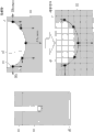
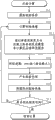
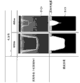
Before to calculation procedure (i), (ii) and (iii) being elaborated, first with reference to Fig. 1 to describing according to the flow process of the whole calculation procedure of the analogy method of the present embodiment.It should be noted that in the present embodiment, will the example of the calculation procedure of the voxel spatial model shown in use Fig. 3 to Fig. 7 be described.In Fig. 3 Zhi Tu7Zhong, shadow region, represent processing target 60.And each in a plurality of rectangular shapes all represents a voxel.
Shape damage calculating part 13 obtains starting condition (condition of for example filling a prescription, device condition, patterning and calculating parameter) (step S1) by input part 11, and calculates the surperficial initial flux (step S2) that enters processing target 60 when t=0.In the calculating of initial flux, for all voxels, the normal vector on surface is that edge is perpendicular to surperficial direction.By utilizing above-mentioned steps to solve the surface reaction model (its specific and nonrestrictive example can be disclosed surface reaction model in document A) of considering depth direction and setting up, the reaction rate (etch-rate or rate of sedimentation) (step S3) while calculating t=0.The value that use calculates, by calculation procedure (iii) by voxel size optimization (step S4).Then, with the reaction rate deriving, carry out shape progress (t → t+dt), and remove or increase voxel (step S5).
And, incident flux by calculation procedure (i) from each voxel is derived the normal vector (step S6) in treatment surface, and the surface reaction model that utilizes the flux total amount in normal vector and normal direction to set up from considering depth direction calculates reaction rate and amount of damage (step S7).Next, by calculation procedure (ii), damage is distributed to voxel (step S8), and, shape progress carried out.When the time (t → t+dt) of shape progress arrives the end time (step S9 is "Yes"), step finishes.When not arriving the end time (step S9 is " no "), judge whether reaction rate (step S10) occurs significantly to change.In the situation significantly changing in reaction rate (being "Yes" in step S10), step proceeds to step S4.In the situation that does not occur significantly to change in reaction rate (step S10 is " no "), step proceeds to step S5.Repeat in this way to calculate until arrive the end time of shape progress.It should be noted that the type of shape progress unrestricted and can be such as being TIGER model, the removable model in existing unit (cell-removable model) etc.
Below will be to calculation procedure (i), (ii) and (iii) be elaborated.For simplicity, below, will carry out basic explanation to being assumed to be two-dimentional calculating.Yet this can easily extend to three-dimensional computations.
[(i) using incident flux computing method vector]
As shown in Figure 3, emphasis is set forth the lip-deep a certain voxel that is arranged in processing target 60, and consideration enters the gas flux of the center of gravity (i, j) of described a certain voxel.Only can consider the flux components that directly enters voxel directly over pattern.In addition, for example also can consider again to penetrate and indirectly enter from pattern sidewalls the flux components of voxel.And, also can consider the impact of wafer percentage of open area, chip open interior rate, local pattern structure etc.The flux vector Γ (i) that now ,Jiang Cong angular direction i enters voxel is along vector of unit length component e
xand e
y(in the situation of three-dimensional computations, be e
x, e
y, e
z) Directional Decomposition, described vector of unit length component e
xand e
ymutually orthogonal, as shown in Figure 3.The flux that other angular direction from each angle step-length are entered is carried out similar operations, and to e
xcomponent summation and to e
ycomponent summation.Finally, by e
xflux components in direction and e
yflux components in direction is synthesized (expression formula 1) with linear mode, and by composite vector Γ
avgdirection be defined as normal direction, and composite vector Γ
avgbe defined as normal vector.In addition, by absolute value | Γ
avg| be defined as the flux total amount with respect to voxel.
By utilizing normal vector Γ
avgthe surface reaction model of setting up considering depth direction (its specific and nonrestrictive example can be disclosed above-mentioned surface reaction model in document A) solves, and calculates reaction rate (etch-rate or rate of sedimentation) and damage.
[(ii) impairment value being distributed to voxel]
Utilize dangling bonds density θ (i, j, R) will damage D
a(i, j, R) is expressed as expression formula 2, damage D
a(i, j, R) is the function apart from the distance R of voxel center of gravity (i, j), and dangling bonds density θ is by for example, obtaining considering that surface reaction model (disclosed above-mentioned surface reaction model in document A) that depth direction is set up solves.
D
a(i,j,R)=V
voxel×θ(i,j,R)×ρ
(expression formula 2)
Herein, V
voxelbe the volume of voxel, and ρ is the density of the etched film of wish.Yet surface reaction model is not limited only to above-mentioned, as long as surface reaction model θ (R).As shown in Figure 4, according to distance R by above-mentioned D
avalue be allocated in a region (in figure dotted line around region), described region has the width (described width is parameterized) perpendicular to normal direction, described distance R Shi Cong point of crossing is to voxel center of gravity (i, j) distance, described point of crossing be normal vector with perpendicular to normal and the Xian point of crossing of extending from being assigned with the center of gravity (i ', j ') of the voxel of damage.
Distributing in the situation of damage in this way, can consider the situation shown in Fig. 5 and Fig. 6.In Fig. 5 and Fig. 6, be primary importance (i, j) 1 adjacent one another are on the surface at processing target 60 and each the computing method vector in the second place (i, j) 2.Particularly, calculate the first method vector at primary importance (i, j) 1 place and second normal vector at the second place (i, j) 2 places.In this kind of situation, the first damage D that first method vector is caused
a1distribute to the voxel existing only in first area, described first area has preset width and comprises first method vector.And, the second damage D that the second normal vector is caused
a2distribute to the voxel existing only in second area, described second area has preset width and comprises described the second normal vector.
In addition in thering is the situation (Fig. 5) that is present in first area and the second area voxel in both and have in the situation (Fig. 6) that is present in the voxel outside first area and second area, damage is allocated as follows.
(1) there is the situation (Fig. 5) that is present in the voxel in first area and second area
(a) be added simply two impairment value (D
a1, D
a2).
(b) distribute the impairment value (D of the center of gravity (i ' j ') of more close associated voxels
a1or D
a2).
(c) take associated voxels is added two impairment values (expression formula 3) with the ratio of first area and the overlapping area (being volume in the situation of three-dimensional computations) of second area respectively.
(d) with respective distance (L apart from the center of gravity of associated voxels (i ', j ')
1, L
2) distribute inversely impairment value (expression formula 4).
(expression formula 4)
(2) there is the situation (Fig. 6) that is present in the voxel outside Liang Ge region
(a) distribute the impairment value (D of the center of gravity (i ', j ') of more close associated voxels
a1or D
a2).
(b) distribute and calculate by interpolation described two impairment values that obtain.For example,, with the respective distance (L of center of gravity apart from associated voxels (i ', j ')
1, L
2) distribute inversely impairment value.
(expression formula 5)
In a kind of distribution method in (a) in the width parameter of range of distribution and above-mentioned (1)~(d) or above-mentioned (2) (a) and (b) in a kind of distribution method when input starting condition, set, and damage information is attached to voxel by the method setting when simulation.
[(iii) optimization of voxel size]
For example, as shown in Figure 7, by initial voxel size (dx
0, dy
0) be set as initial parameter.For example, dx
0can be 1nm and dy
0can be 1nm.Subsequently, in the time period step-length when t=0, utilize the normal vector of derivation in step (i) and the flux total amount effects on surface reaction model in normal direction to solve.The corrected parameter r of voxel size
xand r
ythe vector of unit length component e based on derived
xand e
yreaction rate in direction (etch-rate or rate of sedimentation) ER
xand ER
y, by expression formula 6 and expression formula 7, derive.This means that voxel size is optimised to the size (Fig. 7) of voxel degree of etched (or being deposited) in time period step-length (dt).
(expression formula 6)
(expression formula 7)
For example, the corrected parameter after optimization can be r
x=1 and r
y=3.In addition,, when t=0, the surface that voxel is set for along depth direction from original shape arrives some layers.In the optimized moment that completes above-mentioned voxel size, the memory retention for all voxels, in program, and is calculated to shape and damage distributes subsequently as shown in Figure 1.In the shape of each step-length between progressive stage, at the etch-rate ER that is positioned at the voxel of the first row m row
1min the situation that occurs significantly to change, for example, when meeting following expression formula 8, again by voxel size optimization, particularly, according to the flow process shown in Fig. 1, again define r in step-length t+dt
xand r
y.It should be noted that when obtaining starting condition, in program, set judgement parameter alpha.
(expression formula 8)
According in the above-mentioned computing technique of the present embodiment, produce in advance voxel space, and utilize voxel to calculate shape progress and damage distribution.Yet, for example according to the computing technique of the present embodiment, be also applicable to not have in advance, in the situation (string model) of voxel concept.Particularly, it is the mixture model of string model and voxel model, wherein near new voxel space and the treatment surface being formed by lattice point, is associated, and by the method with in (ii), damage is distributed to voxel space and express damage and distribute.This will set forth (Figure 13 and Figure 14) in a second embodiment.
In addition, according to the computing technique of the present embodiment, be not limited only to be applied to etching, but can be widely used in any treatment step (CVD (the Chemical Vapor Deposition for example that uses plasma; Chemical vapor deposition) and PVD (Physical Vapor Deposition, physical vapour deposition (PVD))).The type of shape progress model can be arbitrary type.
By elaborating, be provided with simulation softward and the treating apparatus (thering is for example visual Simulation result and the function to processing controls automatic feedback) that comprises that step (i), (ii) and shape (iii) and damage distribute and calculate hereinafter in three~five embodiment (Figure 15~17).
[effect]
Use and above-mentionedly according to the analogy method of the present embodiment, can obtain following effect.
(1) the existing voxel model of deriving surface normal with positional information based on adjacent voxels is compared abduction vector more accurately.Therefore, can be with pinpoint accuracy and the high-speed calculating realizing reaction rate (etch-rate, rate of sedimentation), shape and damage distribution.
(2) because damage information also can be attached to voxel, the treatment conditions that therefore damage distributes and is visualized and can utilizes voxel model detailed forecasts in simulation can make damage reduce.Therefore, can predict and the impact of analyzing and processing condition on the electrical characteristics of device in more kinds of modes compared with the conventional method.
(3) because voxel size is optimised to reflect reaction rate, therefore compare with existing voxel model, can lower calculated load come predicting shape and damage to distribute.
(4) processing controls in the time of can carrying out treating apparatus enforcement shape damage simulation with pinpoint accuracy and the in-situ treatment control (described the 4th embodiment and the 5th embodiment vide infra) of using described shape damage simulation.
(5) allow when confirming the analog result that shape and damage distribute and carry out and process, therefore, form turnaround time (the Turn-Around Time for the treatment of conditions; TAT) expection can be shortened (the 4th described embodiment vide infra).
(6) the processing corrected value obtaining by highly accurate simulation and forecast is fed back to treatment conditions successively.Therefore, expection can realize the raising (referring to by the 5th embodiment illustrating below) of the processing of pinpoint accuracy, low damage processing and yield rate.
Next, will according to the actual computation example of the analogy method of the present embodiment, describe using.
[1-2. the first sample calculation (abduction vector Γ in voxel model
avg)]
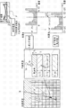
Fig. 8 illustrates the first sample calculation.Fig. 8 illustrates and uses capacitance coupling plasma (Capacitively Coupled Plasma; CCP) dry etching device is to SiO
2the two-dimentional contact etch that film carries out.Use the resist mask that bore dia is 400nm for 200nm and film thickness, voxel size is 3nm * 3nm, and uses following treatment conditions.
(treatment conditions)
Gas type and gas flow: C
4f
8/ O
2/ Ar=11/8/400sccm
Pressure: 30mTorr
Vpp=1450V
Wafer temperature: 30 ℃
Now, use emission spectrum (Optical Emission Spectroscopy; OES), four-electrode spectrum (Quadrupole Mass Spectroscopy; QMS) and infrared diode laser absorption spectrum (Infrared-diode Laser Absorption Spectroscopy; IRLAS) by carrying out plasma monitoring, obtain indoor gas flux data, utilize above-mentioned treatment conditions and described indoor gas flux data, with the state shown in Fig. 8, from ion (CF
+, CF
3 +, CF
2 +, C
2f
4 +, F
+, Ar
+) flux vector and free radical (CF
2, CF, F, CF
3, O) flux vector, utilize above-mentioned calculation procedure (i) to derive the normal vector Γ in two-dimensional space
avg, described ion enters voxel from sidewall and processing bottom, hole.Only consider the flux components directly entering.The angle step of trace is set as to abduction vector Γ in 1 Du,Bing region Φ (Fig. 8)
avg, region Φ extends and comprises that the pattern of expectation is positive from paid close attention to voxel.The normal vector Γ deriving
avgoverlap with the normal vector obtaining by two-dimentional string model (deriving from the positional information of two adjacent lattice points).
[1-3. the second sample calculation (using the simulating shape of the surface reaction model of considering in addition the depth direction in the first sample calculation)]
Fig. 9 illustrates the second sample calculation.In the initial pattern of resist mask, utilize the treatment conditions similar to the first sample calculation (should note, etching period is 160 seconds) carry out treatment of simulated, the bore dia of described resist mask is one of 200nm and 900nm, and has the film thickness of 400nm.Use the normal vector Γ obtaining in the first sample calculation
avgand normal vector Γ
avgthe amount of the flux in direction, depth direction is considered in utilization and the surface reaction model (for example disclosed above-mentioned surface reaction model in document A) set up calculates film thickness and the etch-rate of the reactive deposition thing in each voxel, and calculates shape progress.That in passing, only considers incident ion directly enters (ignoring the scattering effect to patterned surfaces).As shown in Figure 9, at profile scanning electron microscope (Scanning Electron Microscope; SEM) the lower visible processing degree of depth and shape are reproduced.
[1-4. the 3rd sample calculation (optimization of voxel size)]
Figure 10 illustrates the 3rd sample calculation.Figure 10 illustrates initial voxel 61 and by the result of calculation of voxel 62 after initial voxel 61 optimizations.Suppose to carry out contact hole processing under the treatment conditions in above-mentioned the first sample calculation.The initial value of voxel size is (dx
0, dy
0)=(1nm, 1nm).When calculate starting for example, by considering that the surface reaction model (disclosed above-mentioned surface reaction model in document A) of depth direction calculates the etch-rate of vertical direction, the etch-rate of horizontal direction and time period step-length dt are respectively 600nm/min, 10nm/min and 0.3 second.Now, use above-mentioned calculation procedure (iii) to draw r
y=3 and r
x=0.06.Now, r
xenough little.Therefore, for the purpose of reducing memory capacity, by r
xbe set as 1, and be set as making removing the voxel in horizontal direction in a time period step-length, in described time period step-length, the integration etch quantity in horizontal direction surpasses the transverse width of described voxel, and described transverse width is 1nm.
[1-5. the 4th sample calculation (two dimension damage distributes)]
Figure 11 and Figure 12 illustrate the 4th sample calculation.Figure 11 and Figure 12 are shown in the SiO on Si substrate
2(the aspect ratio of aspect ratio in film; AR) be the distribute analog result of (Si crystal defect) of damage that the Si of analog result ,Ji Jiangdui lower floor substrate that 1 contact hole is processed causes.Figure 12 illustrates time dependent analog result by amplifying the surf zone 70 of the bottom of contact hole shown in Figure 11.This is corresponding to lower floor's Si substrate being caused time of damage and carries out the state during etching reaches 3 seconds from starting.Treatment conditions, normal derivation etc. are corresponding with treatment conditions in the above-mentioned first to the 3rd embodiment, normal derivation etc.Adopt the said method 1 (b) in (ii) to distribute damage.
[2. the second embodiment]
Next, the display unit to according to second embodiment of the invention is described.It should be noted that and will suitably omit the explanation similar to above-mentioned the first embodiment.
In above-mentioned the first embodiment, the technology that produces in advance the technology in voxel space and utilize voxel to calculate shape progress and damage distribution is illustrated.Yet in the present embodiment, the concept of voxel is not for initial calculation, and utilizes string model to carry out calculating.Particularly, with comprising that the string model of a plurality of lattice points expresses the surperficial shape of processing target, and utilize string model to carry out the shape progress based on normal vector.Subsequently, at the processing target near surface of expressing by string model, produce voxel space, and be wherein arranged with a plurality of voxels.Based on normal vector, determine the damage that a plurality of incident fluxs cause processing target, and determined damage is distributed to described a plurality of voxel.
Figure 14 diagram is according to the overall procedure of the analogy method of the present embodiment.Shape damage calculating part 13 (Fig. 2) obtains starting condition (condition of for example filling a prescription, device condition, patterning and calculating parameter) (step S11) by input part 11.Shape damage calculating part 13 utilizes string model, passes through the above above-mentioned calculation procedure (i) described in the first embodiment, the normal vector (step S12) incident flux derivation treatment surface.Then, utilize flux total amount in above-mentioned normal vector and normal direction, by considering that the surface reaction model (its concrete and nonrestrictive example can be disclosed above-mentioned surface reaction model in document A) that depth direction is set up calculates reaction rate and amount of damage (step S13).Then, with the reaction rate deriving, carry out shape progress (t → t+dt), and the lattice point in mobile string model (step S14).Then, near the treatment surface of expressing by string model, produce new voxel space (step S15), and distribute to voxel space (step S16) based on above damaging in the above-mentioned calculation procedure (ii) described in the first embodiment.When the time (t → t+dt) of shape progress arrives the end time (step S17 is " be "), step finishes.When the time of shape progress does not arrive the end time (step S17 is " no "), step proceeds to the step in step S12.
Figure 13 illustrates the example of the computation model of shape progress in the present embodiment.For shape progress, use two-dimentional string model.Figure 13 diagram is wherein for example, by processing target 92 (, SiO
2film) and resist 91 be laminated to bottom 93 (for example, Si substrate) and go up and carry out and process to form the example of the model of contact hole.For example, by utilizing flux in normal vector and normal vector direction the surface reaction model (disclosed above-mentioned surface reaction model in document A) of considering depth direction and setting up to be solved to calculate reaction rate (etch-rate or rate of sedimentation) and the impairment value at each lattice point 81 place in string model.Then, voxel space with by being connected the treatment surface 82 that each lattice point 81 forms, be associated.Herein, the size of voxel space (x, y) is determined as follows.The maximal value ERy (max) of vertical component ERy and the maximal value ERx (max) of horizontal component ERx of the reaction rate of retrieval lattice point 81.From being positioned at the lattice point of Shen position, extending to ERy (max) * dt * β and extend to ERx (max) * dt×β region (Figure 13 Zhong shadow region) and be associated with treatment surface 82 as voxel space from being positioned at the lattice point of outermost position.Herein, dt is time period step-length, and β is and the voxel space parameter that phasing closes really.The space that it should be noted that the treatment surface top in normal direction is left in the basket.In this kind of voxel space, by the above-mentioned distribution technique in (ii) described in the first embodiment above, express damage and distribute.
Although it should be noted that in the present embodiment with string model and carry out shape progress, however can be not by string model (string model) but carry out calculating by for example Level Set Models (level-set model).In Level Set Models, analyzed area is divided into lattice shape (mesh shape), each lattice point (grid) is carried out to reactions steps analysis, and usage level set function (level-setfunction) gauging surface shape and over time.
[3. the 3rd embodiment]
Next, the display unit to according to third embodiment of the invention is described.It should be noted that and will suitably omit the explanation similar to above-mentioned the first embodiment and the second embodiment.
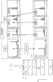
In the present embodiment, will the concrete example of simulation softward (program) be described, described simulation softward is applied the analogy method of above-mentioned the first embodiment or the second embodiment.Figure 15 illustrates the functional configuration example of simulation softward.Simulation softward comprises graphic user interface (Graphical User Interface; GUI) 21 and computing engines portion 22, graphic user interface 21 is for inputting starting condition.Computing engines portion 22 comprises input part 23, plasmoid calculating part 24, shell (sheath) speed-up computation portion 25, percentage of open area calculating part 26, shape damage calculating part 27, efferent 28 and GUI29, input part 23 is for transmitting starting condition value to computing engines portion 22, and GUI29 is used for making analog result visual.
The execution platform of this kind of simulation softward can be any one in for example Windows (registered trademark), Linux (registered trademark), Unix (registered trademark) and Mac (registered trademark).And GUI21 and GUI29 be applicable to any configuration language, for example OpenGL, Motif and tcl/tk.The programming language of computing engines portion 22 can be the programming language of any type, for example C, C
+, Fortran and JAVA (registered trademark).
Formula information, device information, calculating parameter, graphic design system (Graphic Design System; GDS) data and film thickness information are all transfused to from GUI21 as starting condition.Plasmoid calculating part 24 calculates the density of each gas type (ion and free radical) in a large amount of plasmas (bulk plasma) based on starting condition.Ion energy distribution function (ion energy distribution function calculates for the pattern as ion end-state in shell speed-up computation portion 25; IEDF) and angle ion distribution function (ion angular distribution function; IADF), described ion results from described a large amount of plasma and in shell and accelerates (comprising the collision with free radical).For these information, can use the database for example obtaining by actual measurement.
Percentage of open area calculating part 26 calculates wafer percentage of open area and half partially perforation rate (chip open interior rate) to the impact of flux (it is linear) based on GDS data and film thickness information.These incident fluxs based on ion and free radical, shape damage calculating part 27 calculates shape damage according to the calculation process shown in Fig. 1 or Figure 14 and distributes.After calculating finishes, from efferent 28, export the result of the film thickness of the positional information of voxel (processing shape informations such as live width, gradient and mask residual film), damage distribution, reactive deposition thing (polymkeric substance and oxide) to file.And these results also can be visualized by GUI29.Data can be exported or visual in real time in the computing interval.
[4. the 4th embodiment]
Next, the display unit to according to fourth embodiment of the invention is described.It should be noted that and will suitably omit the explanation similar to above-mentioned the first embodiment to the three embodiment.
In the present embodiment, will the structure example of the visual semiconductor processing device that can in real time shape damage be distributed be described, described semiconductor processing device is applied the analogy method of above-mentioned the first embodiment or the second embodiment.Figure 16 illustrates the structure example of semiconductor processing device.
Semiconductor processing device comprises process chamber 32, simulation system 42 and visualization system (GUI37).Process chamber 32 is CCP.Yet process chamber 32 also can be other plasma generation mechanisms, inductively coupled plasma (Inductively Coupled Plasma for example; ICP) type mechanism and electron cyclotron resonace (Electron Cyclotron Resonance; ECR) type mechanism.
[5. the 5th embodiment]
Next, the display unit to according to fifth embodiment of the invention is described.It should be noted that and will suitably omit the explanation similar to the first embodiment to the four embodiment.
In the present embodiment, will describe realizing based on simulation the structure example of the semiconductor processing device of process control system, described semiconductor processing device is applied the analogy method of above-mentioned the first embodiment or the second embodiment.Figure 17 illustrates the structure example of semiconductor processing device.
Semiconductor processing device comprises process chamber 32, simulation system 51, control system 38 and fault detect and classification/assembly project system (Fault Detection and Classification/Equipment Engineering System; FDC/EEC) 39.Process chamber 32 is CCP.Yet process chamber 32 also can be other plasma generation mechanisms, the JiECR of ICPXing mechanism type mechanism for example.
Simulation system 51 comprises gas density and ion energy calculating part 43, percentage of open area calculating part 44, optimization computation system 52 and proofreaies and correct treatment conditions efferent 55.Optimization computation portion 52 comprises shape calculating part 53 and damage calculating part 54.Simulation system 51 has the functional configuration similar in fact to computing engines portion 22 (Figure 15) in above-mentioned the 3rd embodiment.
When shape with damage outside expectation specification time (for example, when the changing value of live width can be expectation value 70nm ± 10% or more than, and amount of damage can increase expectation value 10
11/ cm
250% time), processing parameter can change for example ± 50% (this Rule of judgment value is parameterized) by gas flow, air pressure, the order that applies power and wafer temperature, and can execution graph 1 or Figure 14 in calculating.Therefore, find and can make shape and the correcting condition of damage in expectation specification.By proofreading and correct treatment conditions efferent 55, correcting condition is sent to control system 38.Control system 38 emissioning controling signals are so that process chamber 32 meets correcting condition.Process chamber 32 changes the parameter relevant to correcting condition and proceeds to be processed.If do not find the solution that meets specification in simulation, launch alarm signal to FDC/EES system 39, thereby unit is quit work.
Optimization computation part about simulation system 51, scale while being equal to or greater than the scale of actual treatment time period when section computing time, can be not by finding out optimum solution in line computation shape and damage as mentioned above, but find out by the following method optimum solution: prepare in advance with respect to the shape of various treatment conditions and the database of damage, and utilize described database retrieval interpolation optimum solution.
[6. the 6th embodiment]
Next, the display unit to according to sixth embodiment of the invention is described.It should be noted that and will suitably omit the explanation similar to above-mentioned the first embodiment to the five embodiment.
[the 3rd example (example of the method that etch quantity is quadratured) of 6-1. analogy method]
In the computing technique of the above-mentioned voxel model (TIGER) based on flux method, when carrying out shape progress, for stably removing treatment surface, when calculating beginning, (for example determine large time period step-length, 5s), to remove together whole voxels, described whole voxels comprise having the voxel of slow etch-rate.This is applicable to common voxel model similarly.Therefore, the time period step-length of surface reaction module can have large value, and described value is identical with the value of the time period step-length of shape module.
Yet, generally speaking, to compare with change of shape phenomenon, surface reaction phenomenon betided in the extremely short time period.Therefore, when the step-length of time period is large, not good with respect to the followability of variations of flux, and the degree of accuracy of etch-rate reduces.As a result, analog result can be different from such as true form, actual damage distribution etc. greatly.In addition, even, when setting time period step-length for large value when calculating beginning, when etch-rate also can reduce and can cause etching to be carried out, voxel is not removed.The voxel of once failing to remove can not be removed (as long as using identical step) in the whole computing interval.As a result, the surface of processed shape can have the structure of high roughness.When reducing voxel size and deal with the problems referred to above, particularly, for example when processing the high aspect ratio of contact site and calculate, can make memory space huge.Therefore it is unpractical, setting little voxel.Therefore, expectation provides a kind of shape progress computing technique of new voxel model, and described technology can not reduce voxel size by only reducing time period step-length accurately derives etch-rate.
The problems referred to above can be solved by analogy method hereinafter described.Figure 21 diagram is according to the example of the analogy method of the present embodiment.Figure 19 diagram is by the concept of making progress according to the shape of the analogy method gained of comparative example.Figure 20 diagram is by the concept of making progress according to the shape of the analogy method of the present embodiment.
The structure example of the calculating part in Figure 18 pictorial information treating apparatus (simulator), described signal conditioning package is for realizing the analogy method according to the present embodiment.Similar to the above-mentioned total structure shown in Fig. 2 according to the total structure of the simulator of the present embodiment.Yet shape damage calculating part 13 comprises surface reaction module 63, integration module 64 and shape damage module 65, as shown in figure 18.
According to the maximum feature of the analogy method of the present embodiment, can be: integration module 64 comprises calculating part, described calculating part is for rightly etch quantity and amount of damage being quadratured and kept described etch quantity and amount of damage, and the surface reaction model in surface reaction module 63 is not limited only to above-mentioned person.In addition, the calculating (for example damaging distribution method) in shape damage module 65 is not limited only to above-mentioned person.Surface reaction model hereinafter described and calculating (for example damaging distribution method) are only also example.
Hereinafter with reference to Figure 19 to Figure 21, further set forth according to the details of the analogy method of the present embodiment.
Calculating part 12 (Fig. 2) obtains starting condition (condition of for example filling a prescription, device condition, patterning and calculating parameter) (step S21) by input part 11, and calculates the surperficial initial flux (step S22) that enters processing target 60.And, based on the above-mentioned calculation procedure (i) described in the first embodiment above, from incident flux, derive the normal vector (step S23) treatment surface.
(expression formula 9)
Herein, α (> 0) is judgement parameter (it can be set or can be set in the computing interval when calculate starting), and L is the size of a voxel, and m is the number of the time step of passing by.Condition in meeting expression formula 9 (step S26 for " be ") while carrying out the calculating in shape damage module 65, resets the content of array S (i).When arriving etching during the end time (step S29 for " be "), calculate and finish.When not arriving etching during the end time (step S29 for " no "), step continues.
On the other hand, during condition in not meeting expression formula 9 (step S26 for " no "), do not carry out the reset process of array S (i) and the calculating in shape damage module 65, and proceed directly to next time period step-length (T=T+dt) (step S28) to continue integration step.
As mentioned above, in the analogy method of the present embodiment, integration module 64 in a plurality of time period step-lengths to the etch-rate ER based on as reaction rate
iand amount of damage Da
ishape progress amount (etch quantity ER
i* dT) quadrature.Shape progress amount (∑ ER based on after integration
i* dT), by shape, damage module 65 and carry out shape progress and damage distribution.By this kind of computing method, in little time period step-length, etch quantity is quadratured, and remove successively the voxel (for example, the t=3dt → 4dt in Figure 20) that becomes removable on the surface of processing target 60.In this kind of situation, time period step-length is unrestricted.On the other hand, do not carry out therein in the computation model (Figure 19) of the comparative example of integration step, due to the accuracy problem of etch-rate, may not remove the voxel that should be removed in some cases.
It should be noted that according to the computing technique of the present embodiment and be not limited only to etching, but can be widely used in using any treatment step (for example CVD and PVD) of plasma.Hereinafter will the simulation softward that comprise above-mentioned computing technique and treating apparatus (have analog result visual and function to processing controls automatic feedback) be elaborated.
[effect]
Use can obtain following effect according to the above-mentioned analogy method of the present embodiment.
(1) the accurate etch-rate calculating from detailed surface reaction model and accurate damage are reflected into voxel model, therefore, can realize with higher degree of accuracy shape and damage progress.
(2) can realize with pinpoint accuracy the in-situ treatment control (the second structure example of the first structure example of the described 6-5. treating apparatus that vide infra and 6-6. treating apparatus) of the shape damage simulation of using voxel model.
(3) allow when confirming shape and damage distribution simulation result and carry out and process, therefore, the TAT that forms treatment conditions is expected to shorten (the first structure example of the described 6-5. treating apparatus that vide infra).
(4) the processing corrected value obtaining by highly accurate simulation and forecast is fed back to treatment conditions successively.Therefore, expection can realize the raising of processing, low damage processing and yield rate highly accurately (the second structure example of the described 6-6. treating apparatus that vide infra).
[sample calculation]
Next, will describe wherein using according to the actual computation example of the analogy method of the present embodiment.
[6-2. the first sample calculation (the shape damage simulation of contact etch)]
This sample calculation is that hypothesis is used CPP dry etching unit to SiO
2film carries out the simulation of two-dimentional contact etch.Resist mask has the bore dia of 200nm and the film thickness of 400nm, and the big or small L of voxel is 3nm, and uses following etch process conditions.
(etch process conditions)
Gas type and gas flow: C
4f
8/ O
2/ Ar=11/8/400sccm
Pressure: 30mTorr
Vpp=1450V
Wafer temperature: 30 ℃
In calculating, the time period step-length of surface reaction is 0.01s and α=1.And the calculation process in this sample calculation is as shown in above-mentioned Figure 21.In this example, for the array that etch quantity is quadratured, be S (i), for the array that amount of damage is quadratured, be D (i), and time step be dT.Now, use above-mentioned treatment conditions and by carrying out indoor gas data on flows that plasma monitoring obtains with OES, QMS and IRLAS, utilizing from sidewall and hole and process the ion (CF that enters voxel bottom
+, CF
3 +, CF
2 +, C
2f
4 +, F
+, Ar
+) flux vector and free radical (CF
2, CF, F, CF
3, O) flux vector, for example by the above-mentioned calculation procedure (i) in above-mentioned the first embodiment, abduction is vectorial.Make the amount of the flux in usage vector and normal vector direction, the surface reaction model solution of setting up considering depth direction, and etch-rate and amount of damage when calculating etching period and being 160s.Should note, although the surface reaction model of in this sample calculation, disclosed above-mentioned surface reaction model in document A being set up as considering depth direction, yet the surface reaction model that wish is used is not limited only to this, as long as can calculate etch-rate and amount of damage.
The etch-rate of the voxel at bottom section center is 600nm/min, and removes a voxel by 30 integrations of integration module 64 execution as shown in Figure 18.In this operating period, owing to being formed with the minimum voxel of failing to remove in sidewall of polymeric layer and etch-rate.The hole shape of simulating as shown in figure 22, is used similar treatment conditions to reproduce true form (section SEM).By the above-mentioned calculation procedure (ii) in above-mentioned the first embodiment, carrying out damage distributes.
It should be noted that the type being applied to according to the film of the treatment conditions of the analogy method of the present embodiment, gas flux and wish processing is not limited only to above-mentioned person, and applicable to three-dimensional computations.
[6-3. the second sample calculation is (at contact bed (SiO
2/ Si) near, carry out etching)]
This sample calculation is the sample calculation of the situation that formed by a plurality of processing layers of processing target 60.For example, processing target 60 is shown herein and by the first processing layer 60A and the second processing layer 60B, is formed the sample calculation of the situation of (as shown in figure 23).In this kind of situation being formed by a plurality of processing layers at processing target 60, in shape progress, be considered to occur near two or more processing layer Zhong regions (contact bed), voxel size is different.Although it should be noted that below and will set forth the sample calculation of all processing layers being carried out to the situation of the performed above-mentioned integration step of integration module 64, yet also can only carry out integration step to part layer.For example, in shape progress, be considered to betide in single processing layer Zhong region, can be not by the shape progress amount after integration but use the shape progress corresponding with schedule time step-length to measure to carry out common shape progress, and can in shape progress is considered to occur near two or more processing layer Zhong regions (contact bed), the shape progress based on after integration measure to carry out shape progress.
Figure 24 illustrates the calculation process of this sample calculation.Step in step S31 to S38 in Figure 24 is similar to the above-mentioned steps in the step S21 to S28 in Figure 21.In this sample calculation, calculating part 12 (Fig. 2) comprises determines the step (step S39) of adjusting voxel size and the step (step S40) that resets voxel size by adjusting large little module.When calculating part 12 is not determined adjustment voxel size, calculating part 12 continues steps and does not change voxel size.When calculating part 12, determine while adjusting voxel size, adjust large little module and reset voxel size (step S40), and when arriving etching during the end time (step S41 for " be "), calculate end.When not reaching etching during the end time (step S41 for " no "), move to next time period step-length (T=T+dt) (step S38), and continue step.
The concrete example of adjusting voxel size will be set forth below.Figure 23 is that hypothesis is used CCP dry etching unit to SiO
2the laminated film of/Si carries out etched simulation.SiO
2voxel size L in layer and Si layer is 3nm.And, use following etch process conditions.
(etch process conditions)
Gas type and gas flow: C
4f
8/ O
2/ Ar=6/8/400sccm
Pressure: 30mTorr
Vpp=1450V
Wafer temperature: 39 ℃
When to SiO
2the voxel number that carries out etching and be present in the voxel below with high etch rates becomes for the moment, calculating part 12 determines and adjusts voxel size (step 39 in Figure 24 for " be "), and adjusts large little module and reduce the voxel size (Figure 23) in Si layer.Now, by surface reaction, calculate the SiO in associated voxels
2/ Si selection ratio S, and voxel size is reset into the value that L obtains divided by selection ratio S.In this sample calculation, selection ratio S is 3, and therefore, voxel size is configured to 1nm, is SiO
21/3 of middle voxel size.In the situation that carrying out above-mentioned adjustment size step, by the computing technique shown in Figure 24, carry out simulation.
Although it should be noted that the voxel with high etch rates with acting on the judgment standard of adjusting voxel size, yet judgment standard is not limited only to this.In addition, adjust size and be not limited only to square shape and cubic shape.
[the structure example of 6-4. simulation softward (program)]
The analogy method of the present embodiment is applicable to for example above-mentioned according to the simulation softward of the 3rd embodiment (Figure 15).
Particularly, the damage of the shape in Figure 15 calculating part 27 is carried out the calculating to shape and damage distribution according to the calculation process shown in Figure 21 or Figure 24.After calculating finishes, the result of the film thickness of the positional information of voxel (processing shape information, for example live width, gradient and mask residual film), damage distribution and reactive deposition thing (polymkeric substance and oxide) exports file to from efferent 28.And these results also can be visualized by GUI29.Can to data, export in real time in the computing interval or visual.
[the first structure example of 6-5. treating apparatus]
The analogy method of the present embodiment is applicable to for example above-mentioned according to the treating apparatus of the 4th embodiment (Figure 16).
Particularly, shape damage calculating part 45 in Figure 16 considers that wafer percentage of open area and half partially perforation rate (chip open interior rate) are on the impact of flux (it is linear), and carry out and calculate according to the calculation process shown in Figure 21 or Figure 24, described wafer percentage of open area and described half partially perforation rate utilize GDS and film thickness information 41 to calculate by percentage of open area calculating part 44.During processing, repeat successively above-mentioned steps, and allow and carrying out actual treatment when using the visualization system real-time confirmation change of shape of GUI37 and the prediction of damage distribution.
[the second structure example of 6-6. treating apparatus]
The analogy method of the present embodiment is applicable to for example above-mentioned according to the treating apparatus of the 5th embodiment (Figure 17).
Particularly, the simulation system in Figure 17 51 is calculated shape progress and damage distribution according to the calculation process shown in Figure 21 or Figure 24.
Optimization computation system 52 considers that wafer percentage of open area and half partially perforation rate (chip open interior rate) are on the impact of flux (it is linear), and calculating etch-rate and damage distribution by the calculation process shown in Figure 21 or Figure 24, described wafer percentage of open area and described half partially perforation rate utilize GDS and film thickness information 41 to calculate by percentage of open area calculating part 44.
When shape and damage are outside expectation specification (for example, when the changing value of live width can be expectation value 70nm ± 10% or above and amount of damage can increase expectation value 10
11/ cm
250% time), processing parameter can change for example ± 50% (this Rule of judgment value is parameterized) by gas flow, air pressure, the order that applies power and wafer temperature, and can carry out the calculating in Figure 21 or Figure 24.Therefore, find and can in expectation specification, realize the correcting condition of shape and damage.By proofreading and correct treatment conditions efferent 55, correcting condition is sent to control system 38.Control system 38 emissioning controling signals are so that process chamber 32 meets correcting condition.Process chamber 32 changes the parameter relevant to correcting condition and continues to be processed.If do not find the solution that meets specification in simulation, launch alarm signal to FDC/EES system 39, thereby device is quit work.
[7. the 7th embodiment]
Next, the display unit to according to seventh embodiment of the invention is described.It should be noted that and will suitably omit the explanation similar to above-mentioned the first embodiment to the six embodiment.
[the 4th example of 7-1. analogy method (considering the example of the computing method that IEDF and IADE change)]
Generally speaking, in the simulating shape of semiconductor processes, the incident flux effects on surface reaction being incident to by the ion of plasma generation and the pattern of free radical by utilization solves to calculate etch-rate.Therefore, highly accurate Shape Prediction may need highly accurate etch-rate computing technique.Now, how at full speed and pinpoint accuracy the ion energy distribution function of incident ion (IEDF) and angle ion distribution function (IADF) are carried out modeling and are incorporated in calculating becoming key.The IEDF of surperficial ion 74 and the example of IADF that Figure 25 diagram enters processing target 60.When ion 74 is during through shell region (being applied with the region of high-frequency electric field), ion 74 repeatedly collides and passes through applied bias voltage and enter pattern Processing when repeatedly accelerating at the free radical particle with around.Now, and then, after ion 74 passes shell region, be known that ionic flux has the three-dimensional spatial distribution of energy and angle (as shown in figure 25).
The high energy component of ionic flux has narrow Incident angle distribution, and therefore, described high energy component is shape bottom to be made to the component of main contributions.Low energy component has wide Incident angle distribution, and therefore, its sidewall sections to shape is made main contributions.Therefore,, when predicting the processing shape causing because of ion 74 with pinpoint accuracy and damaging distribution, advantageously consider IEDF and IADF, and further consider IEDF and the IADF variation during processing.
About the modeling of the IEDF for surface reaction and IADE, for example, in document B (No. 2004-266098th, uncensored Japanese Patent Application Publication case), a kind of technology is disclosed.In the disclosed technology of document B, first, when shape calculate to start, first carry out the energy integral relevant to IEDF (ignore incident ionic energy along with during processing in treatment surface the increase of formed deposited film and the model that reduces), and only set about comprising the function of angle θ in the pattern front of expectation.Consider the variation (that is, the variation of θ) of Incident angle distribution and carry out the calculating to etch-rate, the variation of described Incident angle distribution is caused by the change of shape along with treatment progress.Therefore, can realize supercomputing.
Yet disclosed above-mentioned technology is to use the technology of carrying out the ionic flux of energy integral when calculating beginning in document B.Therefore, in document B, disclosed technology should not be applied to the processing that the high aspect-ratio pattern that significantly changes occurs during processing for incident gas flux for example, or is applied to be formed at the treatment step that the thickness of lip-deep deposited film (polymkeric substance or oxide) changes at during etching.Causing a reason of this kind of situation is that etch-rate may may be reduced greatly by the degree of accuracy of overestimate and Shape Prediction in some cases.
In addition, when ion invades in the deposited film in treatment surface, or while further invading in the responding layer of its below, can be because the ion energy up to hundreds of eV is lost in the scattering of atom around.This according to IEDF on depth direction kind of variation, IADF also can occur significantly to change.Yet disclosed above-mentioned technology has also been ignored described effect in document B, therefore, exist about being difficult to accurately predicting etch-rate and being difficult to the problem of accurately predicting shape.
Owing to for example, making pattern microminiaturized according to the improvement (reducing the damage that substrate is caused) of apparatus function recently, therefore need to be accurate to nano level processing Shape Prediction technology etc.Therefore, 3D shape damage analogue technique has caused people's concern.In such cases, expect a kind of can considering rightly in IEDF and both variations of IADF at full speed and the computing technique of pinpoint accuracy predicting shape and damage during processing.
The problems referred to above can be solved by analogy method hereinafter described.Figure 26 diagram is according to the example of the analogy method of the present embodiment.It should be noted that for realizing according to the total structure of the signal conditioning package of the analogy method of the present embodiment (simulator) similar to person described in Fig. 2, and the calculating shown in the calculation process carried out in Figure 26 of shape damage calculating part 13.
In the present embodiment, calculate shape when progress damaging calculating part 13 by shape, for example, can use the voxel model similar to the voxel model of above-mentioned the first embodiment.Yet, also can use other models (for example string model and Level Set Models).As surface reaction model, for example, can use the surface reaction model (flat plate model) (for example above-mentioned surface reaction model described in document A) of considering depth direction and setting up.
Figure 27 illustrates the example of flat plate model.In flat plate model, responding layer 72 region is divided into a plurality of thin flat boards 73 along depth direction, and obtains the surface reaction of each flat board 73.In the flat plate model shown in Figure 27, responding layer 72 is formed at deposited film 71 belows.For example,, by SiO
2film carries out as processing target in the situation of dry etching, when for example using gas based on CF as etching gas, at SiO
2the polymeric layer that comprises carbon (C) in the surface of film forms deposited film 71.As shown in figure 27, when the thickness of deposited film 71 is Tn, from the surface of deposited film 71 to the thickness T of the j flat board 73 of lower floor ' be Tn+L (1)+L (2)+... L (j).L (j) is the thickness of j flat board 73.
According to the analogy method of the present embodiment, comprise the steps (the step S53 in Figure 26): when ion 74 is through being formed at the lip-deep deposited film 71 of processing target and when being formed at the responding layer 72 of deposited film 71 belows, calculating the variation of IEDF and the variation of IADF.According to the analogy method of the present embodiment, also comprise the steps:, when ion 74 passes deposited film 71 and responding layer 72, when considering the variation of IEDF and the variation of IADF, to calculate ionic flux.According to the analogy method of the present embodiment, also comprise by predetermined surface reaction model being solved to calculate the step (the step S55 in Figure 26) of reaction rate of predetermined process and the step (the step S56 in Figure 26) of carrying out the shape progress of computing target based on described reaction rate.According to the analogy method of the present embodiment, also comprise the step (the step S58 in Figure 26) of the variation of calculating the thickness of deposited film Tn causing due to shape progress, and use the variation of the film thickness Tn of deposited film as index, to recalculate the step of the variation of IEDF and the variation of IADF.
To elaborate the analogy method according to the present embodiment according to the calculation process in Figure 26 below.It should be noted that according to the maximum of the analogy method of the present embodiment and be characterised in that, described analogy method comprises the step of considering the variation of ion energy distribution function and the variation of angle ion distribution function and calculating incident flux.Calculating (for example distribution method of damage) is not limited only to above described in the first embodiment.
Shape damage calculating part 13 (Fig. 2) obtains starting condition (formula condition, device condition, patterning and calculating parameter) (step S51) by input part 11.After obtaining starting condition, by shell calculate or actual measurement create ion 74 at it just through the IEDF after shell region and the database (step S52) of IADF.As another, select, create the function f (θ, E) of IEDF and IADF.In this example, θ is the estimation angle from associated voxels to pattern front, and E is the energy of ion 74.
Next step calculates (step S53) to the incident ion flux being present in each voxel in treatment surface.Now, the IADF in the variation that calculating produces due to shape correlativity (θ correlativity), the variation of the IEDF in each flat board and each flat board changes.And, calculate the free radical flux (step S54) in each voxel.Based on above-mentioned information, carry out planar surface Response calculation (step S55).As planar surface Response calculation, such as calculating etch-rate as reaction rate, amount of damage etc.When arriving etching during the end time (step S57 for " be "), calculate and finish.
When not arriving etching during the end time (step S57 for " no "), use the thickness T n (n: the number of time step) condition based in following expression 10 is determined the renewal (step S58) in IEDF and IADF as parameter of deposited film.Herein, α is Rule of judgment and can be for example 0.2 (self-evident, the value of α is not limited only to according to 0.2 of computing application).If meet expression formula 10 (step S58 for " be "), upgrade the variation of IEDF and the variation of IADF, if do not meet expression formula 10 (step S58 for " no "), do not carry out and upgrade and only consider because planar surface Response calculation (step S59 and S55) is carried out in the variation that shape correlativity produces.Repeat above-mentioned calculating until time period step-length corresponding to etching period.
(expression formula 10)
Next will the technology that IEDF changes and IADF changes of calculating in flat board be described.
[calculating that IEDF changes]
At ion during through deposited film 71 and responding layer 72, consider reducing of ion energy and the variation of calculating as follows IEDF.Figure 28 illustrates the concept of the technology of calculating IEDF variation.As shown in figure 28, the energy E of ion 74 itself reduces Δ E (T ') according to the thickness of deposited film (Tn) and the dull and stereotyped gross thickness (θ L (j)) that is positioned at deposited film below.Now, at ion 74, just through after shell region, and then from the reference database of IEDF, read the amount of flux of correlation energy or read the functional value as shown in expression formula 11.
(expression formula 11)
[calculating the variation of IADF]
As mentioned above, variation to IADF is calculated, and makes the total amount of the incident ion flux in the second angular range of IADF when ion 74 enters deposited film 71 total amount of the incident ion flux in the first angular range of preceding IADF equals ion 74 through responding layer 72 immediately.
Figure 29 illustrates the concept of the technology of calculating IADF variation.Incident immediately the first angular range of preceding IADF be that the expected angle θ 1 being started by the arbitrary voxel from being present in treatment surface defines with θ 2.During IADF in determining j flat board 73, first, obtain the functional value as shown in expression formula 11.Subsequently, determine the second new angular range [0, θ 1 "]; [0; θ 2 "] (expression formula 14), make by the second angular range around area equal by above-mentioned the first angular range around area (S1L, S1R), and make with respect to the second angular range in the vertical direction angulation in region, the area on right direction to the ratio of the area on left direction and the first angular range the ratio in region equate (expression formula 13).S2R be by the second angular range around right direction on area, and S2L be by the second angular range around left direction on area.
S1L+S1R=S2L+S2R
(expression formula 12)
S1L/S1R=S2L/S2R
(expression formula 13)
In this way, the IEDF that can be at high speed calculates the ion 74 in processed film with analysis mode changes and IADF changes and do not use Monte Carlo method.
In the computing technique of the present embodiment, suppose that ion just remains in the IEDF and IADF in processed film through the information behind shell region.In other words, suppose that the scattering mechanism in shell region is identical with the scattering mechanism in processed film.It is below a reason that causes this kind of situation.That is,, in shell region, ion 74 has the scattering mechanism that ion 74 and its free radical around collided and obtained simultaneously the biased energy of executing repeatedly.Yet, consider that applied bias voltage has minimum limit value, therefore collision becomes leading factor, and can think that the scattering of ion 74 in shell region is similar to the scattering of ion 74 in processed film.In addition, in common treatment step, can estimate the scattering number of ion 74 in shell region (thering is the thickness of several millimeters) no better than ion 74 the scattering number in processed film (thickness with some nanometers).
Hereinafter will simulation softward and the treating apparatus (having such as visual Simulation result and the functions such as automatic feedback to processing controls) that is provided with above-mentioned computing technique be elaborated.
[effect]
Use can obtain following effect according to the above-mentioned analogy method of the present embodiment.
(1) different from the step based on common Monte Carlo method, according to the analogy method of the present embodiment, be to calculate the analytical technology that IEDF changes and IADF changes.Therefore, can realize the supercomputing (can realize the simplification of calculating) to shape damage progress.
(2) by using according to the analogy method of the present embodiment and in conjunction with the computing technique of above-mentioned the first embodiment, can realize the in-situ treatment of using the shape damage simulation of voxel model and carrying out with pinpoint accuracy and control (the second structure example of the first structure example of the described 7-5. treating apparatus that vide infra and 7-6. treating apparatus).
(3) allow when confirming shape and damage distribution simulation result and carry out and process, therefore, the TAT that forms treatment conditions is expected to be shortened (the first structure example of the described 7-5. treating apparatus that vide infra).
(4) the processing corrected value obtaining by highly accurate simulation and forecast is fed back to treatment conditions successively.Therefore, be expected to realize the raising of processing, low damage processing and yield rate highly accurately (the second structure example of the described 7-6. treating apparatus that vide infra).
[sample calculation]
Next, will according to the actual computation example of the analogy method of the present embodiment, describe using.
[7-2. the first sample calculation (is calculated etching SiO
2iEDF during planar film changes and IADF changes)]
This sample calculation is that hypothesis utilizes CCP dry etching device to SiO
2planar film is carried out etched simulation.In calculating, use following etch process conditions, with lower device condition and following condition of plasma.
(etch process conditions)
Gas type and gas flow: C
4f
8/ O
2/ Ar=11/8/400sccm
Pressure: 30mTorr
Wafer temperature: 30 ℃
(device condition and condition of plasma)
Top applies frequency: 60MHz
Bottom applies frequency: 2MHz
Bottom applies bias voltage: 700V
Plasma potential: 20V
Self-bias voltage :-700V
Plasma density: 5 * 10
10/ cm
3
Electron temperature: 3eV
Use above-mentioned condition, by considering that the shell of the vibration of shell in shell region and free radical scattering calculates, and creates the reference database of IEDF and IADF.The database of IADF creates for the energy of every 50eV, and the quantification bandwidth of angle (bin width) is 1 degree (part in the upper right portion data in graph form storehouse of Figure 30).It should be noted that in document A, the disclosed above-mentioned surface reaction model (flat plate model) of considering depth direction and setting up calculates for surface reaction.The time period step-length of surface reaction is set to 0.01s, and the thickness of a flat board 73 is set to 0.5nm, and dull and stereotyped number is set to 15.
The etching state of Figure 30 diagram when reaction reaches steady state (SS).Now be formed at SiO
2deposited film 71 (polymeric layer) on film is that 0.1nm is thick.Ion 74 enters deposited film 71 and at the SiO of each flat board 73
2when being scattered in film, advance.Yet, for example, on the surface of for example the 9th flat board (j=9), CF2
+in ion, there is the energy attenuation of 700V, and now as shown in the lower right-most portion of Figure 30, calculate the variation of IEDF and the variation of IADF.Use each the ion (CF in each flat board 73
+, CF
3 +, CF
2 +, C
2f
4 +, F
+, Ar
+) IEDF and IADF and free radical (CF
2, CF, F, CF
3and O) result that flux calculates etch-rate gained is 540nm/min, and this equates with the value obtaining in actual measurement.Although it should be noted that by using OES, QMS and IRLAS to carry out data that indoor plasma monitoring obtains as the value of incident flux, yet select as another, can use the amount of flux calculating by computer simulated plasma.
In addition,, in above-mentioned example, by utilizing Monte Carlo method to carry out shell calculating, create the IEDF of incident ion 74 and the reference database of IADF in advance.Yet, also can use the function (depending on ion energy and incident angle) of for example, deriving from analytical solution (Maxell (Maxwell) distributes).The type of the film that wish is processed is not limited only to SiO
2, and also can realize calculating when using such as Si film, SiN film, organic film, compound film etc.Applicable etch processes, applicable device and applicable condition of plasma are not limited only to above-mentioned.
[7-3. the second sample calculation (the shape damage simulation of contact etch)]
This sample calculation is that hypothesis utilizes CCP dry etching device to SiO
2film carries out the simulation of two-dimentional contact etch.At bore dia, be in two kinds of situations of 400nm and 900nm, to use the resist mask with 400nm film thickness, and voxel model is for shape progress (voxel size L is 3nm).Use following etch process conditions.Device condition and condition of plasma are similar to above-mentioned the first sample calculation.
(etch process conditions)
Gas type and gas flow: C
4f
8/ O
2/ Ar=33/8/400sccm
Pressure: 30mTorr
Vpp=1450V
Wafer temperature: 30 ℃
Calculation process in this sample calculation is as shown in above-mentioned Figure 26.α is set to 0.1, and the time period step-length of surface reaction in calculating is set to 0.01s.Now, use above-mentioned treatment conditions and the indoor gas flux data by using OES, QMS and IRLAS to carry out plasma monitoring to obtain, for example by the above-mentioned calculation procedure (i) in the first embodiment, enter the ion (CF of voxel in bottom process in sidewall Ji Cong hole
+, CF
3 +, CF
2 +, C
2f
4 +, F
+, Ar
+) flux vector and free radical (CF
2, CF, F, CF
3, O) flux vector abduction vector.The surface reaction model solution that the amount of the flux in usage vector and normal vector direction is set up considering depth direction, thereby processing shape and amount of damage when calculating etching period and being 230s.Although it should be noted that and use the surface reaction model that in document A, disclosed above-mentioned surface reaction model is set up as considering depth direction, yet the surface reaction model that wish is used is not limited only to this, as long as can calculate etch-rate and amount of damage.
The hole shape of simulating as shown in figure 31, is used similar treatment conditions to reproduce true form (section SEM).By the above-mentioned calculation procedure (ii) in the first embodiment, carrying out damage distributes.Partly there is discontinuous hole shape part in the inner side of the cut-open view of the true form of 400nm shown in Figure 31.Yet, equally with analog result in other sections confirm there is continuous hole shape.
It should be noted that the type being applicable to according to the processed film of the treatment conditions of the analogy method of the present embodiment, gas flux and wish is not limited only to above-mentioned person.In addition, foregoing can similarly be applied to three-dimensional computations.Shape progress model can be other string models or can be Level Set Models.
[the structure example of 7-4. simulation softward (program)]
According to the analogy method of the present embodiment applicable to for example above-mentioned according to the simulation softward of the 3rd embodiment (Figure 15).
Particularly, the shape shown in Figure 15 damage calculating part 27 considers that according to the calculation process shown in Figure 26 the variation of ion energy distribution function and the variation of angle ion distribution function calculate shape damage and distribute.After calculating finishes, from efferent 28, export the result of the film thickness of the positional information of voxel (processing shape information, for example live width, gradient and mask residual film), damage distribution, reactive deposition thing (polymkeric substance and oxide) to file.And these results can be visualized by GUI29.Can to data, export in real time in the computing interval or visual.
[the first structure example of 7-5. treating apparatus]
According to the analogy method of the present embodiment applicable to for example above-mentioned according to the treating apparatus of the 4th embodiment (Figure 16).
Particularly, shape shown in Figure 16 damage calculating part 45 comprises the module of calculating for carrying out the ionic flux shown in the calculation process of Figure 26, and carries out the calculating of considering that IEDF changes and IADF changes shape damage distributes.Shape damage calculating part 45 considers that wafer percentage of open area and half partially perforation rate are on the impact of flux (it is linear), and carry out and calculate according to the calculation process shown in Figure 26, described wafer percentage of open area and described half partially perforation rate utilize GDS and film thickness information to calculate by percentage of open area calculating part.During processing, repeat successively this step, and allow in the prediction distributing by GUI visualization system real-time confirmation change of shape and damage and carry out actual treatment.
[the second structure example of 7-6. treating apparatus]
According to the analogy method of the present embodiment applicable to for example above-mentioned according to the treating apparatus of the 5th embodiment (Figure 17).
Particularly, the optimization computation system 52 shown in Figure 17 comprises the module of calculating for carrying out the ionic flux shown in the calculation process of Figure 26, and carries out the calculating of considering that IEDF changes and IADF changes shape damage distributes.On process chamber 32, be provided with for obtaining OES33, QMS34, IRLAS35 and the energy depressive spectroscopy 36 of simulation required input data, and during processing, pass through said modules continuous monitoring plasma.Sampling rate can be for example 0.1s.The information of obtaining by said modules during processing and formula information 31 are sent to simulation system 51, and calculate gas density, IEDF and IADF.When computing time section be enough shorter than actual treatment during the time period, all these all can be determined by reactor simulation.And, optimization computation portion 52 considers that wafer percentage of open area and half partially perforation rate (chip open interior rate) are on the impact of flux (it is linear), and calculating etch-rate and damage distribution according to the calculation process shown in Figure 26, described wafer percentage of open area and described half partially perforation rate utilize GDS and film thickness information 41 to calculate by percentage of open area calculating part 44.
When shape and damage are outside expectation specification (for example, when the changing value of live width can be expectation value 70nm ± 10% or above and amount of damage can increase expectation value 10
11/ cm
250% time), processing parameter can change for example ± 50% (this Rule of judgment value is parameterized) by gas flow, air pressure, the order that applies power and wafer temperature, and can carry out the calculating in Figure 26.Therefore, find and can in expectation specification, realize the correcting condition of shape and damage.By proofreading and correct treatment conditions efferent 55, correcting condition is sent to control system 38.Control system 38 emissioning controling signals are so that process chamber 32 meets correcting condition.Process chamber 32 changes the parameter relevant to correcting condition and continues to be processed.If do not find the solution that meets specification in simulation, launch alarm signal to FDC/EES system 39, thereby device is quit work.
[8. other embodiment]
Technology according to the present invention is not limited only to the above explanation to each embodiment, but can make various variations.Each in above-described embodiment represents the example of preferred exemplary of the present invention, and technical scope of the present invention is not limited only to above-described embodiment.For example, the present invention can be widely used in using semiconductor processes and the semiconductor manufacturing cell of plasma.Can widespread use and irrelevant with type of device according to analogy method of the present invention, simulator program and treating apparatus.
According to above-mentioned exemplary embodiment of the present invention and version, can at least realize following structure.
(1) make signal conditioning package carry out an analogy method of calculating, described calculating comprises:
Each in a plurality of incident fluxs is resolved into the flux components in each mutually orthogonal vector of unit length direction, and described a plurality of incident fluxs locate to enter the surface of processing target at an arbitrary position, and described processing target is the target of predetermined process;
In each of described a plurality of vector of unit length directions to described flux components summation; And
A plurality of flux components are synthesized to a vector, and described a plurality of flux components are summations in described each vector of unit length direction and mutually orthogonal, thereby calculate the normal vector of the described lip-deep described any position of described processing target.
(2) analogy method as described in (1), described calculating also comprises:
Produce voxel space, and utilize a plurality of voxels to express the shape of described processing target; And
Based on described normal vector, determine the damage that described a plurality of incident flux causes described processing target, and described determined damage is distributed to described a plurality of voxels.
(3) analogy method as described in (2), described calculating also comprises:
Based on starting condition, set each the initial voxel size in described voxel; And
According to the reaction rate on the described surface of described processing target, carry out initial voxel size described in optimization, described reaction rate is to utilize described normal vector to calculate.
(4) analogy method as described in (2) or (3), described calculating also comprises:
On the described surface of described processing target, calculate the normal vector of primary importance and the normal vector of the second place, thereby determine the first method vector at described primary importance place and second normal vector at described second place place;
The first damage that described first method vector is caused is distributed to as one of described a plurality of voxels and exists only in the voxel in first area, and described first area has preset width and comprises described first method vector; And
The second damage that described the second normal vector is caused is distributed to as one of described a plurality of voxels and exists only in the voxel in second area, and described second area has preset width and comprises described the second normal vector.
(5) analogy method as described in (4), when described a plurality of voxels comprise that while being present in overlapping voxel in both of described first area and described second area, described calculating also comprises:
By by described the first damage and the damage obtaining of adding up of described the second ratio that damages to be scheduled to are distributed to described overlapping voxel.
(6) analogy method as described in (4), when described a plurality of voxels comprise that while being present in overlapping voxel in both of described first area and described second area, described calculating also comprises:
Described overlapping voxel is distributed in the damage that normal vector of more close described overlapping voxel in described first method vector and described the second normal vector is caused.
(7) analogy method as described in (4), when described a plurality of voxels comprise that while being present in outside voxel outside both of described first area and described second area, described calculating also comprises:
To damage and by interpolation, calculate obtained damage and distribute to described outside voxel based on described the first damage and described second.
(8) analogy method as described in (4), when described a plurality of voxels comprise that while being present in outside voxel outside both of described first area and described second area, described calculating also comprises:
Described outside voxel is distributed in the damage that normal vector of more close described outside voxel in described first method vector and described the second normal vector is caused.
(9) analogy method as described in any one in (1) to (8), described calculating also comprises:
Utilization comprises that the string model of a plurality of lattice points expresses the shape on the described surface of described processing target, and utilizes described string model to simulate shape progress based on described normal vector;
Utilizing the described near surface of the expressed described processing target of described string model to produce voxel space, and arranging a plurality of voxels in described voxel space; And
Based on described normal vector, determine the damage that described a plurality of incident flux causes described processing target, and determined described damage is distributed to described a plurality of voxel.
(10) analogy method as described in any one in (1) to (9), described calculating also comprises:
Flux total amount effects on surface reaction model in direction based on described normal vector and described normal vector solves, described surface reaction model is to consider the described direction of described normal vector and set up, thereby calculates the reaction rate of described predetermined process or the damage described processing target being caused by described a plurality of incident fluxs.
(11) analogy method as described in any one in (1) to (8), described calculating also comprises:
Produce voxel space and utilize a plurality of voxels to express the shape of described processing target;
Based on described normal vector to predetermined surface reaction model solution, thereby calculate the reaction rate of described predetermined process in predetermined time section step-length;
Described reaction rate based in a plurality of time period step-lengths is carried out integration to shape progress amount; And
Described shape progress based on after integration measures to simulate the described shape progress on described a plurality of voxel.
(12) analogy method as described in (11), described calculating also comprises:
Based on described normal vector, obtain described predetermined surface reaction model, thereby calculate the damage that described processing target is caused in described predetermined time section step-length;
In a plurality of time period step-lengths, described determined damage is carried out to integration; And
The described damage being integrated is distributed to described a plurality of voxel.
(13) analogy method as described in (11) or (12), wherein, the described simulation of described shape progress is comprised to whether the described integration amount that judge described shape progress meets the big or small predetermined condition that depends on voxel described in one of them, and comprise that when the described integration amount of making progress when described shape meets described predetermined condition, carrying out described shape makes progress.
(14) analogy method as described in any one in (11) to (13), wherein
Described processing target comprises a plurality of processing layers of being made by different materials, and
The described expression of the described shape of described processing target being carried out with described a plurality of voxels comprises: when described shape progress arrives, wherein predict when two the above processing layers being carried out to the region of described shape progress, change for expressing the size of the described voxel of described two above processing layers.
(15) analogy method as described in any one in (11) to (14), wherein
Described processing target comprises a plurality of processing layers of being made by different materials,
The described simulation of described shape progress comprises: predict therein and will in the single processing layer in described a plurality of processing layers, carry out in the region of described shape progress, amount based on the corresponding described shape progress of described predetermined time section step-length but not described shape progress based on after described integration measures to simulate described shape progress, and predict therein and will two the above processing layers be carried out in the region of described shape progress, the described shape progress based on after described integration measures to simulate described shape progress.
(16) analogy method as described in any one in (1) to (10), described calculating also comprises:
Ion through be formed at the described lip-deep deposited film of described processing target and described processing target be formed at the responding layer below described deposited film time, calculate the variation of ion energy distribution function and the variation of angle ion distribution function; And
Consider that the described variation of described ion energy distribution function and the described variation of described angle ion distribution function calculate described a plurality of incident flux.
(17) analogy method as described in (16), described calculating also comprises:
Based on described normal vector to predetermined surface reaction model solution, thereby calculate the reaction rate of described predetermined process;
Based on described reaction rate, calculate the shape progress of described processing target;
Calculating is by the variation in thickness of the caused described deposited film of described shape progress; And
Utilize the value of the described variation in thickness of described deposited film again to calculate the described variation of described ion energy distribution function and the described variation of described angle ion distribution function as parameter.
(18) analogy method as described in (16) or (17), wherein, the step of calculating the described variation of described angle ion distribution function comprises: calculate the described variation of described angle ion distribution function so that described ion enter described deposited film immediately the total amount of the incident ion flux of preceding described angle ion distribution function in the first angular range equal described ion when the described responding layer described in the total amount of the incident ion flux of angle ion distribution function in the second angular range.
(19) analogy method as described in any one in (16) to (18), wherein, the described variation that while considering described ion through described deposited film and described responding layer, described ion energy distribution function is calculated in the minimizing of ion energy.
(20) analogy method as described in any one in (1) to (19), wherein,
Described predetermined process is the step for semiconductor processes; And
Consider that one or more in the impact of wafer percentage of open area, chip open interior rate and local pattern structure calculates described a plurality of incident flux.
(21) according to the analogy method described in any one in (1) to (20), wherein, the described calculating of described a plurality of incident fluxs comprises: consider that the component on the described surface that directly enters described processing target in described any position and the one or both indirectly entering in described any position in the component on described surface of described processing target calculate described normal vector.
(22) according to the analogy method described in any one in (1) to (21), wherein
Described predetermined process is the processing that utilizes plasma to carry out semiconductor, and
One or both during the calculating of plasma gas phase and shell calculate is reflected into the described calculating of described normal vector.
(23) store a nonvolatile computer-readable medium for simulator program, described simulator program makes signal conditioning package carry out calculating, and described calculating comprises:
Each in a plurality of incident fluxs is resolved into the flux components in each mutually orthogonal vector of unit length direction, and described a plurality of incident fluxs locate to enter the surface of processing target at an arbitrary position, and described processing target is the target of predetermined process;
In each of described a plurality of vector of unit length directions to described flux components summation; And
A plurality of flux components are synthesized to a vector, and described a plurality of flux components are summations in described each vector of unit length direction and mutually orthogonal, thereby calculate the normal vector of the described lip-deep described any position of described processing target.
(24), it comprises:
Handling part, it is for carrying out predetermined process to processing target; And
Simulator, it is for simulating described predetermined process and carrying out and calculate, and described calculating comprises:
Each in a plurality of incident fluxs is resolved into the flux components in each mutually orthogonal vector of unit length direction, and described a plurality of incident fluxs locate to enter the surface of described processing target at an arbitrary position;
In each of described a plurality of vector of unit length directions to described flux components summation; And
A plurality of flux components are synthesized to a vector, and described a plurality of flux components are summations in described each vector of unit length direction and mutually orthogonal, thereby calculate the normal vector of the described lip-deep described any position of described processing target.
(25) treating apparatus as described in (24), wherein,
Described simulator comprises input part, and described input part is used for obtaining for carrying out the treatment conditions of described predetermined process, and
The described treatment conditions of being obtained by described input part comprise the information obtaining by monitoring the performed described processing of described handling part.
(26) treating apparatus as described in (24), wherein, described simulator comprises efferent, described efferent is for exporting the analog result of described predetermined process.
(27) treating apparatus as described in (26), also comprises control part, and described control part is for proofreading and correct based on described analog result for carry out the described treatment conditions of described predetermined process by described handling part.
(28), described simulator comprises calculating part, and described calculating part is for simulating the performed predetermined process of processing target and carrying out and calculate, and described calculating comprises:
Each in a plurality of incident fluxs is resolved into the flux components in each mutually orthogonal vector of unit length direction, and described a plurality of incident fluxs locate to enter the surface of processing target at an arbitrary position;
In each of described a plurality of vector of unit length directions to described flux components summation; And
A plurality of flux components are synthesized to a vector, and described a plurality of flux components are summations in described each vector of unit length direction and mutually orthogonal, thereby calculate the normal vector of the described lip-deep described any position of described processing target.
Disclosed Topic relative in the Japanese priority patent application case JP2012-146065 that the theme that the application's case comprises and in June, 2012,28Xiang Japan Office filed an application and the Japanese priority patent application case JP2013-014556 that in January, 2013,29Xiang Japan Office filed an application, the full content of described two Japanese priority patent application cases is incorporated herein by reference.
Those skilled in the art will appreciate that, can to the present invention, make various modifications, combination, sub-portfolio and change according to designing requirement and other factors, as long as it belongs in the scope of enclose claims or its equivalent.
Claims (20)
1. make signal conditioning package carry out an analogy method of calculating, described calculating comprises:
Each in a plurality of incident fluxs is resolved into the flux components in each mutually orthogonal vector of unit length direction, and described a plurality of incident fluxs locate to enter the surface of processing target at an arbitrary position, and described processing target is the target of predetermined process;
In each of described a plurality of vector of unit length directions to described flux components summation; And
A plurality of flux components are synthesized to a vector, and described a plurality of flux components are summations in described each vector of unit length direction and mutually orthogonal, thereby calculate the normal vector of the described lip-deep described any position of described processing target.
2. analogy method as claimed in claim 1, described calculating also comprises:
Produce voxel space, and utilize a plurality of voxels to express the shape of described processing target; And
Based on described normal vector, determine the damage that described a plurality of incident flux causes described processing target, and determined described damage is distributed to described a plurality of voxel.
3. analogy method as claimed in claim 2, described calculating also comprises:
Based on starting condition, set each the initial voxel size in described voxel; And
According to the reaction rate on the described surface of described processing target, carry out initial voxel size described in optimization, described reaction rate is to utilize described normal vector to calculate.
4. analogy method as claimed in claim 2, described calculating also comprises:
Calculate the normal vector of described lip-deep primary importance and the normal vector of the second place of described processing target, thereby determine the first method vector at described primary importance place and second normal vector at described second place place;
The first damage that described first method vector is caused is distributed to as one of described a plurality of voxels and exists only in the voxel in first area, and described first area has preset width and comprises described first method vector; And
The second damage that described the second normal vector is caused is distributed to as one of described a plurality of voxels and exists only in the voxel in second area, and described second area has preset width and comprises described the second normal vector.
5. analogy method as claimed in claim 4, when described a plurality of voxels comprise that while being present in overlapping voxel in both of described first area and described second area, described calculating also comprises:
Described overlapping voxel is distributed in the damage that ratio addition by described the first damage and described second is damaged to be scheduled to is obtained.
6. analogy method as claimed in claim 4, when described a plurality of voxels comprise that while being present in overlapping voxel in both of described first area and described second area, described calculating also comprises:
Described overlapping voxel is distributed in the damage that normal vector of more close described overlapping voxel in described first method vector and described the second normal vector is caused.
7. analogy method as claimed in claim 4, when described a plurality of voxels comprise that while being present in outside voxel outside both of described first area and described second area, described calculating also comprises:
To damage and by interpolation, calculate obtained damage and distribute to described outside voxel based on described the first damage and described second.
8. analogy method as claimed in claim 4, when described a plurality of voxels comprise that while being present in outside voxel outside both of described first area and described second area, described calculating also comprises:
Described outside voxel is distributed in the damage that normal vector of more close described outside voxel in described first method vector and described the second normal vector is caused.
9. analogy method as claimed in claim 1, described calculating also comprises:
Utilization comprises that the string model of a plurality of lattice points expresses the shape on the described surface of described processing target, and utilizes described string model to simulate shape progress based on described normal vector;
Utilizing the described near surface of the expressed described processing target of described string model to produce voxel space, and arranging a plurality of voxels in described voxel space; And
Based on described normal vector, determine the damage that described a plurality of incident flux causes described processing target, and determined described damage is distributed to described a plurality of voxel.
10. analogy method as claimed in claim 1, described calculating also comprises:
Flux total amount effects on surface reaction model in direction based on described normal vector and described normal vector solves, described surface reaction model is to consider the described direction of described normal vector and set up, thereby calculates the reaction rate of described predetermined process or the damage described processing target being caused by described a plurality of incident fluxs.
11. analogy methods as claimed in claim 1, described calculating also comprises:
Produce voxel space and utilize a plurality of voxels to express the shape of described processing target;
Based on described normal vector to predetermined surface reaction model solution, thereby calculate the reaction rate of described predetermined process in predetermined time section step-length;
Described reaction rate based in a plurality of time period step-lengths is carried out integration to shape progress amount; And
Described shape progress based on after integration measures to simulate the described shape progress on described a plurality of voxel.
12. analogy methods as claimed in claim 11, described calculating also comprises:
Based on described normal vector to described predetermined surface reaction model solution, thereby in described predetermined time section step-length, calculate the damage that described processing target is caused;
In a plurality of time period step-lengths, determined described damage is carried out to integration; And
Described damage after integration is distributed to described a plurality of voxel.
13. analogy methods as claimed in claim 11, the described simulation of described shape progress is comprised to whether described shape progress amount judge after integration meets the big or small predetermined condition that depends on one of described voxel, and the described shape progress amount after described integration of comprising is carried out described shape while meeting described predetermined condition and is made progress.
14. analogy methods as claimed in claim 11,
Described processing target comprises a plurality of processing layers of being made by different materials, and
The described expression of the described shape of described processing target being carried out with described a plurality of voxels comprises: when described shape progress arrives, wherein predict when two the above processing layers being carried out to the region of described shape progress, change for expressing the size of the described voxel of described two above processing layers.
15. analogy methods as claimed in claim 11,
Described processing target comprises a plurality of processing layers of being made by different materials,
The described simulation of described shape progress comprises: predict therein and will in the single processing layer in described a plurality of processing layers, carry out in the region of described shape progress, amount based on the corresponding described shape progress of described predetermined time section step-length but not described shape progress based on after described integration measures to simulate described shape progress, and predict therein and will two the above processing layers be carried out in the region of described shape progress, the described shape progress based on after described integration measures to simulate described shape progress.
16. analogy methods as claimed in claim 1, described calculating also comprises:
Ion through be formed at the described lip-deep deposited film of described processing target and described processing target be formed at the responding layer below described deposited film time, calculate the variation of ion energy distribution function and the variation of angle ion distribution function; And
Consider that the described variation of described ion energy distribution function and the described variation of described angle ion distribution function calculate described a plurality of incident flux.
17. analogy methods as claimed in claim 16, described calculating also comprises:
Based on described normal vector to predetermined surface reaction model solution, thereby calculate the reaction rate of described predetermined process;
Based on described reaction rate, calculate the shape progress of described processing target;
Calculating is by the variation in thickness of the caused described deposited film of described shape progress; And
Utilize the value of the described variation in thickness of described deposited film again to calculate the described variation of described ion energy distribution function and the described variation of described angle ion distribution function as parameter.
18. 1 kinds for storing the nonvolatile computer-readable medium of simulator program, and described simulator program is carried out signal conditioning package to calculate, and described calculating comprises:
Each in a plurality of incident fluxs is resolved into the flux components in each mutually orthogonal vector of unit length direction, and described a plurality of incident fluxs locate to enter the surface of processing target at an arbitrary position, and described processing target is the target of predetermined process;
In each of described a plurality of vector of unit length directions to described flux components summation; And
A plurality of flux components are synthesized to a vector, and described a plurality of flux components are summations in described each vector of unit length direction and mutually orthogonal, thereby calculate the normal vector of the described lip-deep described any position of described processing target.
19. 1 kinds for the treatment of apparatus, it comprises:
Handling part, it is for carrying out predetermined process to processing target; And
Simulator, it is for simulating described predetermined process and carrying out and calculate, and described calculating comprises:
Each in a plurality of incident fluxs is resolved into the flux components in each mutually orthogonal vector of unit length direction, and described a plurality of incident fluxs locate to enter the surface of described processing target at an arbitrary position;
In each of described a plurality of vector of unit length directions to described flux components summation; And
A plurality of flux components are synthesized to a vector, and described a plurality of flux components are summations in described each vector of unit length direction and mutually orthogonal, thereby calculate the normal vector of the described lip-deep described any position of described processing target.
20. 1 kinds of simulators, it comprises calculating part, and described calculating part is for simulating the predetermined process that processing target is carried out and carrying out and calculate, and described calculating comprises:
Each in a plurality of incident fluxs is resolved into the flux components in each mutually orthogonal vector of unit length direction, and described a plurality of incident fluxs locate to enter the surface of processing target at an arbitrary position;
In each of described a plurality of vector of unit length directions to described flux components summation; And
A plurality of flux components are synthesized to a vector, and described a plurality of flux components are summations in described each vector of unit length direction and mutually orthogonal, thereby calculate the normal vector of the described lip-deep described any position of described processing target.
Applications Claiming Priority (4)
| Application Number | Priority Date | Filing Date | Title |
|---|---|---|---|
| JP2012146065 | 2012-06-28 | ||
| JP2012-146065 | 2012-06-28 | ||
| JP2013-014556 | 2013-01-29 | ||
| JP2013014556A JP6065612B2 (en) | 2012-06-28 | 2013-01-29 | Simulation method, simulation program, processing apparatus and simulator |
Publications (1)
| Publication Number | Publication Date |
|---|---|
| CN103514318A true CN103514318A (en) | 2014-01-15 |
Family
ID=49778985
Family Applications (1)
| Application Number | Title | Priority Date | Filing Date |
|---|---|---|---|
| CN201310247610.7A Pending CN103514318A (en) | 2012-06-28 | 2013-06-20 | Simulation method, computer-readable medium, processing unit, and simulator |
Country Status (3)
| Country | Link |
|---|---|
| US (1) | US9189577B2 (en) |
| JP (1) | JP6065612B2 (en) |
| CN (1) | CN103514318A (en) |
Cited By (1)
| Publication number | Priority date | Publication date | Assignee | Title |
|---|---|---|---|---|
| CN112068398A (en) * | 2019-06-11 | 2020-12-11 | 佳能株式会社 | Simulation method, simulation apparatus, storage medium, film formation method, and method for producing cured product |
Families Citing this family (11)
| Publication number | Priority date | Publication date | Assignee | Title |
|---|---|---|---|---|
| JP5685762B2 (en) * | 2011-03-07 | 2015-03-18 | みずほ情報総研株式会社 | Plasma processing shape simulation apparatus and program |
| US20150013901A1 (en) * | 2013-07-11 | 2015-01-15 | Hsio Technologies, Llc | Matrix defined electrical circuit structure |
| US20150205890A1 (en) * | 2014-01-17 | 2015-07-23 | Kabushiki Kaisha Toshiba | Topography simulation apparatus, topography simulation method and recording medium |
| JP6117746B2 (en) * | 2014-07-30 | 2017-04-19 | ソニーセミコンダクタソリューションズ株式会社 | Etching characteristic estimation method, program, information processing apparatus, processing apparatus, design method, and manufacturing method |
| US10534355B2 (en) * | 2015-02-20 | 2020-01-14 | Sony Semiconductor Solutions Corporation | Information processing device, processing device, prediction method, and processing method |
| US10599789B2 (en) * | 2015-11-25 | 2020-03-24 | Synopsys, Inc. | Topography simulation of etching and/or deposition on a physical structure |
| JP2017162286A (en) | 2016-03-10 | 2017-09-14 | 東芝メモリ株式会社 | Shape simulation device, shape simulation method, and shape simulation program |
| JP2017163035A (en) * | 2016-03-10 | 2017-09-14 | 東芝メモリ株式会社 | Shape simulation device, shape simulation method, and shape simulation program |
| JP2018067677A (en) * | 2016-10-21 | 2018-04-26 | ソニーセミコンダクタソリューションズ株式会社 | Damage prediction method, program, and semiconductor processing system |
| US11093665B2 (en) * | 2017-10-25 | 2021-08-17 | Lockheed Martin Corporation | System and method for simulation visualization |
| CN113378444B (en) * | 2021-08-13 | 2021-11-05 | 墨研计算科学(南京)有限公司 | Method and device for simulating deposition process |
Family Cites Families (12)
| Publication number | Priority date | Publication date | Assignee | Title |
|---|---|---|---|---|
| JPH03188926A (en) | 1989-12-19 | 1991-08-16 | Kubota Corp | Filtration treatment method |
| JP2687270B2 (en) | 1992-07-27 | 1997-12-08 | 日本電信電話株式会社 | Display method of semiconductor device sectional structure |
| JP3188926B2 (en) | 1993-09-06 | 2001-07-16 | 日本電信電話株式会社 | Display method of semiconductor device sectional structure |
| US6313842B1 (en) * | 1999-03-03 | 2001-11-06 | Discreet Logic Inc. | Generating image data |
| JP3388203B2 (en) * | 1999-05-28 | 2003-03-17 | 株式会社半導体先端テクノロジーズ | Shape simulation method, apparatus and recording medium |
| US7375490B2 (en) * | 2004-09-14 | 2008-05-20 | Siemens Energy & Automation, Inc. | Methods for managing electrical power |
| US7850338B1 (en) * | 2006-09-25 | 2010-12-14 | Microscan Systems, Inc. | Methods for directing light |
| JP4957195B2 (en) * | 2006-11-09 | 2012-06-20 | ソニー株式会社 | Liquid crystal display |
| JP5322413B2 (en) * | 2007-08-16 | 2013-10-23 | 株式会社東芝 | Simulation method and simulation program |
| JP5428450B2 (en) * | 2009-03-30 | 2014-02-26 | ソニー株式会社 | Ion irradiation damage prediction method, ion irradiation damage simulator, ion irradiation apparatus and ion irradiation method |
| JP2011081154A (en) * | 2009-10-07 | 2011-04-21 | Hitachi Ltd | Optical element and optical apparatus |
| US9905028B2 (en) * | 2013-12-11 | 2018-02-27 | Adobe Systems Incorporated | Simulating sub-surface scattering of illumination for simulated three-dimensional objects |
-
2013
- 2013-01-29 JP JP2013014556A patent/JP6065612B2/en active Active
- 2013-06-17 US US13/919,470 patent/US9189577B2/en active Active
- 2013-06-20 CN CN201310247610.7A patent/CN103514318A/en active Pending
Cited By (2)
| Publication number | Priority date | Publication date | Assignee | Title |
|---|---|---|---|---|
| CN112068398A (en) * | 2019-06-11 | 2020-12-11 | 佳能株式会社 | Simulation method, simulation apparatus, storage medium, film formation method, and method for producing cured product |
| CN112068398B (en) * | 2019-06-11 | 2024-03-15 | 佳能株式会社 | Simulation method, simulation apparatus, storage medium, film forming method, and method for producing cured product |
Also Published As
| Publication number | Publication date |
|---|---|
| JP2014029982A (en) | 2014-02-13 |
| JP6065612B2 (en) | 2017-01-25 |
| US9189577B2 (en) | 2015-11-17 |
| US20140005990A1 (en) | 2014-01-02 |
Similar Documents
| Publication | Publication Date | Title |
|---|---|---|
| CN103514318A (en) | Simulation method, computer-readable medium, processing unit, and simulator | |
| US11704463B2 (en) | Method of etch model calibration using optical scatterometry | |
| JP6899659B2 (en) | Methods and equipment for etching profile optimization by reflection spectrum matching and surface kinetic model optimization | |
| TWI805580B (en) | Design layout pattern proximity correction through edge placement error prediction | |
| CN107526864B (en) | Photoresist design layout pattern proximity correction via edge placement error prediction | |
| TWI851567B (en) | Methods, systems, and computer program products for optimizing process simulation models | |
| US9881107B2 (en) | Simulation method, simulation program, processing apparatus, simulator, and design method | |
| US20170176983A1 (en) | Methods and apparatuses for etch profile matching by surface kinetic model optimization | |
| CN109388842A (en) | Method and apparatus through reflected light matching and surface dynamic model optimization etching outline | |
| US8535550B2 (en) | Shape simulation apparatus, shape simulation program, semiconductor production apparatus, and semiconductor device production method | |
| US9881104B2 (en) | Simulating shape of a workpiece based on a flux | |
| Kokkoris et al. | Simulation of SiO 2 and Si feature etching for microelectronics and microelectromechanical systems fabrication: A combined simulator coupling modules of surface etching, local flux calculation, and profile evolution | |
| JP6173889B2 (en) | Simulation method, simulation program, machining control system, simulator, process design method and mask design method | |
| KR20140016924A (en) | Device for estimating and simulating shape worked by plasma process, and simulation method and program | |
| Xiao et al. | Multiscale modeling and neural network model based control of a plasma etch process | |
| Guo et al. | Optimizing Plasma Etching: Integrating Precise Three-Dimensional Etching Simulation and Machine Learning for Multi-Objective Optimization | |
| Ertl | Numerical methods for topography simulation | |
| Rodrigues et al. | Surface reaction and topography modeling of fluorocarbon plasma etching |
Legal Events
| Date | Code | Title | Description |
|---|---|---|---|
| C06 | Publication | ||
| PB01 | Publication | ||
| C02 | Deemed withdrawal of patent application after publication (patent law 2001) | ||
| WD01 | Invention patent application deemed withdrawn after publication |
Application publication date: 20140115 |