CN102498546A - Film formation apparatus - Google Patents
Film formation apparatus Download PDFInfo
- Publication number
- CN102498546A CN102498546A CN2010800411155A CN201080041115A CN102498546A CN 102498546 A CN102498546 A CN 102498546A CN 2010800411155 A CN2010800411155 A CN 2010800411155A CN 201080041115 A CN201080041115 A CN 201080041115A CN 102498546 A CN102498546 A CN 102498546A
- Authority
- CN
- China
- Prior art keywords
- plasma
- film formation
- substrate
- partition wall
- formation device
- Prior art date
- Legal status (The legal status is an assumption and is not a legal conclusion. Google has not performed a legal analysis and makes no representation as to the accuracy of the status listed.)
- Pending
Links
- 230000015572 biosynthetic process Effects 0.000 title claims abstract description 144
- 238000005192 partition Methods 0.000 claims abstract description 182
- 239000007789 gas Substances 0.000 claims abstract description 158
- 239000000758 substrate Substances 0.000 claims abstract description 136
- 230000007246 mechanism Effects 0.000 claims abstract description 24
- 230000004913 activation Effects 0.000 claims description 25
- 238000009616 inductively coupled plasma Methods 0.000 claims description 24
- 238000006243 chemical reaction Methods 0.000 claims description 15
- 230000009471 action Effects 0.000 claims description 8
- 230000008878 coupling Effects 0.000 claims description 8
- 238000010168 coupling process Methods 0.000 claims description 8
- 238000005859 coupling reaction Methods 0.000 claims description 8
- 239000012495 reaction gas Substances 0.000 claims description 6
- 230000008859 change Effects 0.000 claims description 5
- 239000001257 hydrogen Substances 0.000 claims description 4
- 229910052739 hydrogen Inorganic materials 0.000 claims description 4
- 238000007789 sealing Methods 0.000 claims description 3
- 125000004435 hydrogen atom Chemical class [H]* 0.000 claims description 2
- 150000003377 silicon compounds Chemical class 0.000 claims description 2
- 239000010408 film Substances 0.000 abstract description 144
- 239000010409 thin film Substances 0.000 abstract description 4
- 239000000376 reactant Substances 0.000 abstract 4
- 230000003213 activating effect Effects 0.000 abstract 2
- 239000012159 carrier gas Substances 0.000 abstract 1
- 238000005755 formation reaction Methods 0.000 description 129
- 239000003595 mist Substances 0.000 description 36
- 229910021419 crystalline silicon Inorganic materials 0.000 description 22
- 230000000694 effects Effects 0.000 description 17
- 150000003254 radicals Chemical class 0.000 description 12
- 229910052710 silicon Inorganic materials 0.000 description 8
- 239000010703 silicon Substances 0.000 description 8
- XUIMIQQOPSSXEZ-UHFFFAOYSA-N Silicon Chemical compound [Si] XUIMIQQOPSSXEZ-UHFFFAOYSA-N 0.000 description 7
- 229910021417 amorphous silicon Inorganic materials 0.000 description 7
- 238000000034 method Methods 0.000 description 7
- 239000002184 metal Substances 0.000 description 6
- 229910052751 metal Inorganic materials 0.000 description 6
- 238000005516 engineering process Methods 0.000 description 5
- 238000007348 radical reaction Methods 0.000 description 5
- 150000004756 silanes Chemical class 0.000 description 5
- 238000005229 chemical vapour deposition Methods 0.000 description 4
- 239000004020 conductor Substances 0.000 description 4
- 239000000203 mixture Substances 0.000 description 4
- 239000008188 pellet Substances 0.000 description 4
- 230000009467 reduction Effects 0.000 description 4
- 238000003860 storage Methods 0.000 description 4
- 150000001450 anions Chemical class 0.000 description 3
- 230000033228 biological regulation Effects 0.000 description 3
- 238000002425 crystallisation Methods 0.000 description 3
- XKRFYHLGVUSROY-UHFFFAOYSA-N Argon Chemical compound [Ar] XKRFYHLGVUSROY-UHFFFAOYSA-N 0.000 description 2
- UFHFLCQGNIYNRP-UHFFFAOYSA-N Hydrogen Chemical compound [H][H] UFHFLCQGNIYNRP-UHFFFAOYSA-N 0.000 description 2
- BLRPTPMANUNPDV-UHFFFAOYSA-N Silane Chemical compound [SiH4] BLRPTPMANUNPDV-UHFFFAOYSA-N 0.000 description 2
- 150000001768 cations Chemical class 0.000 description 2
- 230000002950 deficient Effects 0.000 description 2
- 238000007599 discharging Methods 0.000 description 2
- 230000005284 excitation Effects 0.000 description 2
- 239000011521 glass Substances 0.000 description 2
- 230000006698 induction Effects 0.000 description 2
- 238000004519 manufacturing process Methods 0.000 description 2
- 239000000463 material Substances 0.000 description 2
- 230000002093 peripheral effect Effects 0.000 description 2
- 238000005268 plasma chemical vapour deposition Methods 0.000 description 2
- 230000008569 process Effects 0.000 description 2
- 238000004904 shortening Methods 0.000 description 2
- 238000004088 simulation Methods 0.000 description 2
- TVEXGJYMHHTVKP-UHFFFAOYSA-N 6-oxabicyclo[3.2.1]oct-3-en-7-one Chemical compound C1C2C(=O)OC1C=CC2 TVEXGJYMHHTVKP-UHFFFAOYSA-N 0.000 description 1
- RYGMFSIKBFXOCR-UHFFFAOYSA-N Copper Chemical compound [Cu] RYGMFSIKBFXOCR-UHFFFAOYSA-N 0.000 description 1
- -1 Silicon compound Chemical class 0.000 description 1
- 229910052786 argon Inorganic materials 0.000 description 1
- 238000001816 cooling Methods 0.000 description 1
- 229910052802 copper Inorganic materials 0.000 description 1
- 239000010949 copper Substances 0.000 description 1
- 238000005520 cutting process Methods 0.000 description 1
- 238000000280 densification Methods 0.000 description 1
- 238000010586 diagram Methods 0.000 description 1
- 230000003028 elevating effect Effects 0.000 description 1
- 238000000605 extraction Methods 0.000 description 1
- 239000012467 final product Substances 0.000 description 1
- 239000012530 fluid Substances 0.000 description 1
- 150000002431 hydrogen Chemical class 0.000 description 1
- OUUQCZGPVNCOIJ-UHFFFAOYSA-N hydroperoxyl Chemical compound O[O] OUUQCZGPVNCOIJ-UHFFFAOYSA-N 0.000 description 1
- 238000009413 insulation Methods 0.000 description 1
- 150000002500 ions Chemical class 0.000 description 1
- 239000011159 matrix material Substances 0.000 description 1
- 230000003287 optical effect Effects 0.000 description 1
- 229920000642 polymer Polymers 0.000 description 1
- 238000006116 polymerization reaction Methods 0.000 description 1
- 230000001105 regulatory effect Effects 0.000 description 1
- 230000000452 restraining effect Effects 0.000 description 1
Images


Classifications
-
- C—CHEMISTRY; METALLURGY
- C23—COATING METALLIC MATERIAL; COATING MATERIAL WITH METALLIC MATERIAL; CHEMICAL SURFACE TREATMENT; DIFFUSION TREATMENT OF METALLIC MATERIAL; COATING BY VACUUM EVAPORATION, BY SPUTTERING, BY ION IMPLANTATION OR BY CHEMICAL VAPOUR DEPOSITION, IN GENERAL; INHIBITING CORROSION OF METALLIC MATERIAL OR INCRUSTATION IN GENERAL
- C23C—COATING METALLIC MATERIAL; COATING MATERIAL WITH METALLIC MATERIAL; SURFACE TREATMENT OF METALLIC MATERIAL BY DIFFUSION INTO THE SURFACE, BY CHEMICAL CONVERSION OR SUBSTITUTION; COATING BY VACUUM EVAPORATION, BY SPUTTERING, BY ION IMPLANTATION OR BY CHEMICAL VAPOUR DEPOSITION, IN GENERAL
- C23C16/00—Chemical coating by decomposition of gaseous compounds, without leaving reaction products of surface material in the coating, i.e. chemical vapour deposition [CVD] processes
- C23C16/44—Chemical coating by decomposition of gaseous compounds, without leaving reaction products of surface material in the coating, i.e. chemical vapour deposition [CVD] processes characterised by the method of coating
- C23C16/4412—Details relating to the exhausts, e.g. pumps, filters, scrubbers, particle traps
-
- C—CHEMISTRY; METALLURGY
- C23—COATING METALLIC MATERIAL; COATING MATERIAL WITH METALLIC MATERIAL; CHEMICAL SURFACE TREATMENT; DIFFUSION TREATMENT OF METALLIC MATERIAL; COATING BY VACUUM EVAPORATION, BY SPUTTERING, BY ION IMPLANTATION OR BY CHEMICAL VAPOUR DEPOSITION, IN GENERAL; INHIBITING CORROSION OF METALLIC MATERIAL OR INCRUSTATION IN GENERAL
- C23C—COATING METALLIC MATERIAL; COATING MATERIAL WITH METALLIC MATERIAL; SURFACE TREATMENT OF METALLIC MATERIAL BY DIFFUSION INTO THE SURFACE, BY CHEMICAL CONVERSION OR SUBSTITUTION; COATING BY VACUUM EVAPORATION, BY SPUTTERING, BY ION IMPLANTATION OR BY CHEMICAL VAPOUR DEPOSITION, IN GENERAL
- C23C16/00—Chemical coating by decomposition of gaseous compounds, without leaving reaction products of surface material in the coating, i.e. chemical vapour deposition [CVD] processes
- C23C16/44—Chemical coating by decomposition of gaseous compounds, without leaving reaction products of surface material in the coating, i.e. chemical vapour deposition [CVD] processes characterised by the method of coating
- C23C16/448—Chemical coating by decomposition of gaseous compounds, without leaving reaction products of surface material in the coating, i.e. chemical vapour deposition [CVD] processes characterised by the method of coating characterised by the method used for generating reactive gas streams, e.g. by evaporation or sublimation of precursor materials
- C23C16/452—Chemical coating by decomposition of gaseous compounds, without leaving reaction products of surface material in the coating, i.e. chemical vapour deposition [CVD] processes characterised by the method of coating characterised by the method used for generating reactive gas streams, e.g. by evaporation or sublimation of precursor materials by activating reactive gas streams before their introduction into the reaction chamber, e.g. by ionisation or addition of reactive species
-
- C—CHEMISTRY; METALLURGY
- C23—COATING METALLIC MATERIAL; COATING MATERIAL WITH METALLIC MATERIAL; CHEMICAL SURFACE TREATMENT; DIFFUSION TREATMENT OF METALLIC MATERIAL; COATING BY VACUUM EVAPORATION, BY SPUTTERING, BY ION IMPLANTATION OR BY CHEMICAL VAPOUR DEPOSITION, IN GENERAL; INHIBITING CORROSION OF METALLIC MATERIAL OR INCRUSTATION IN GENERAL
- C23C—COATING METALLIC MATERIAL; COATING MATERIAL WITH METALLIC MATERIAL; SURFACE TREATMENT OF METALLIC MATERIAL BY DIFFUSION INTO THE SURFACE, BY CHEMICAL CONVERSION OR SUBSTITUTION; COATING BY VACUUM EVAPORATION, BY SPUTTERING, BY ION IMPLANTATION OR BY CHEMICAL VAPOUR DEPOSITION, IN GENERAL
- C23C16/00—Chemical coating by decomposition of gaseous compounds, without leaving reaction products of surface material in the coating, i.e. chemical vapour deposition [CVD] processes
- C23C16/44—Chemical coating by decomposition of gaseous compounds, without leaving reaction products of surface material in the coating, i.e. chemical vapour deposition [CVD] processes characterised by the method of coating
- C23C16/455—Chemical coating by decomposition of gaseous compounds, without leaving reaction products of surface material in the coating, i.e. chemical vapour deposition [CVD] processes characterised by the method of coating characterised by the method used for introducing gases into reaction chamber or for modifying gas flows in reaction chamber
- C23C16/45502—Flow conditions in reaction chamber
-
- C—CHEMISTRY; METALLURGY
- C23—COATING METALLIC MATERIAL; COATING MATERIAL WITH METALLIC MATERIAL; CHEMICAL SURFACE TREATMENT; DIFFUSION TREATMENT OF METALLIC MATERIAL; COATING BY VACUUM EVAPORATION, BY SPUTTERING, BY ION IMPLANTATION OR BY CHEMICAL VAPOUR DEPOSITION, IN GENERAL; INHIBITING CORROSION OF METALLIC MATERIAL OR INCRUSTATION IN GENERAL
- C23C—COATING METALLIC MATERIAL; COATING MATERIAL WITH METALLIC MATERIAL; SURFACE TREATMENT OF METALLIC MATERIAL BY DIFFUSION INTO THE SURFACE, BY CHEMICAL CONVERSION OR SUBSTITUTION; COATING BY VACUUM EVAPORATION, BY SPUTTERING, BY ION IMPLANTATION OR BY CHEMICAL VAPOUR DEPOSITION, IN GENERAL
- C23C16/00—Chemical coating by decomposition of gaseous compounds, without leaving reaction products of surface material in the coating, i.e. chemical vapour deposition [CVD] processes
- C23C16/44—Chemical coating by decomposition of gaseous compounds, without leaving reaction products of surface material in the coating, i.e. chemical vapour deposition [CVD] processes characterised by the method of coating
- C23C16/455—Chemical coating by decomposition of gaseous compounds, without leaving reaction products of surface material in the coating, i.e. chemical vapour deposition [CVD] processes characterised by the method of coating characterised by the method used for introducing gases into reaction chamber or for modifying gas flows in reaction chamber
- C23C16/45563—Gas nozzles
- C23C16/45574—Nozzles for more than one gas
-
- C—CHEMISTRY; METALLURGY
- C23—COATING METALLIC MATERIAL; COATING MATERIAL WITH METALLIC MATERIAL; CHEMICAL SURFACE TREATMENT; DIFFUSION TREATMENT OF METALLIC MATERIAL; COATING BY VACUUM EVAPORATION, BY SPUTTERING, BY ION IMPLANTATION OR BY CHEMICAL VAPOUR DEPOSITION, IN GENERAL; INHIBITING CORROSION OF METALLIC MATERIAL OR INCRUSTATION IN GENERAL
- C23C—COATING METALLIC MATERIAL; COATING MATERIAL WITH METALLIC MATERIAL; SURFACE TREATMENT OF METALLIC MATERIAL BY DIFFUSION INTO THE SURFACE, BY CHEMICAL CONVERSION OR SUBSTITUTION; COATING BY VACUUM EVAPORATION, BY SPUTTERING, BY ION IMPLANTATION OR BY CHEMICAL VAPOUR DEPOSITION, IN GENERAL
- C23C16/00—Chemical coating by decomposition of gaseous compounds, without leaving reaction products of surface material in the coating, i.e. chemical vapour deposition [CVD] processes
- C23C16/44—Chemical coating by decomposition of gaseous compounds, without leaving reaction products of surface material in the coating, i.e. chemical vapour deposition [CVD] processes characterised by the method of coating
- C23C16/50—Chemical coating by decomposition of gaseous compounds, without leaving reaction products of surface material in the coating, i.e. chemical vapour deposition [CVD] processes characterised by the method of coating using electric discharges
- C23C16/505—Chemical coating by decomposition of gaseous compounds, without leaving reaction products of surface material in the coating, i.e. chemical vapour deposition [CVD] processes characterised by the method of coating using electric discharges using radio frequency discharges
- C23C16/509—Chemical coating by decomposition of gaseous compounds, without leaving reaction products of surface material in the coating, i.e. chemical vapour deposition [CVD] processes characterised by the method of coating using electric discharges using radio frequency discharges using internal electrodes
-
- H—ELECTRICITY
- H01—ELECTRIC ELEMENTS
- H01J—ELECTRIC DISCHARGE TUBES OR DISCHARGE LAMPS
- H01J37/00—Discharge tubes with provision for introducing objects or material to be exposed to the discharge, e.g. for the purpose of examination or processing thereof
- H01J37/32—Gas-filled discharge tubes
- H01J37/32009—Arrangements for generation of plasma specially adapted for examination or treatment of objects, e.g. plasma sources
- H01J37/32082—Radio frequency generated discharge
-
- H—ELECTRICITY
- H01—ELECTRIC ELEMENTS
- H01J—ELECTRIC DISCHARGE TUBES OR DISCHARGE LAMPS
- H01J37/00—Discharge tubes with provision for introducing objects or material to be exposed to the discharge, e.g. for the purpose of examination or processing thereof
- H01J37/32—Gas-filled discharge tubes
- H01J37/32431—Constructional details of the reactor
- H01J37/3244—Gas supply means
-
- H—ELECTRICITY
- H01—ELECTRIC ELEMENTS
- H01J—ELECTRIC DISCHARGE TUBES OR DISCHARGE LAMPS
- H01J37/00—Discharge tubes with provision for introducing objects or material to be exposed to the discharge, e.g. for the purpose of examination or processing thereof
- H01J37/32—Gas-filled discharge tubes
- H01J37/32431—Constructional details of the reactor
- H01J37/32532—Electrodes
- H01J37/32568—Relative arrangement or disposition of electrodes; moving means
-
- H—ELECTRICITY
- H01—ELECTRIC ELEMENTS
- H01J—ELECTRIC DISCHARGE TUBES OR DISCHARGE LAMPS
- H01J37/00—Discharge tubes with provision for introducing objects or material to be exposed to the discharge, e.g. for the purpose of examination or processing thereof
- H01J37/32—Gas-filled discharge tubes
- H01J37/32431—Constructional details of the reactor
- H01J37/32623—Mechanical discharge control means
- H01J37/32633—Baffles
-
- H—ELECTRICITY
- H01—ELECTRIC ELEMENTS
- H01L—SEMICONDUCTOR DEVICES NOT COVERED BY CLASS H10
- H01L31/00—Semiconductor devices sensitive to infrared radiation, light, electromagnetic radiation of shorter wavelength or corpuscular radiation and specially adapted either for the conversion of the energy of such radiation into electrical energy or for the control of electrical energy by such radiation; Processes or apparatus specially adapted for the manufacture or treatment thereof or of parts thereof; Details thereof
- H01L31/04—Semiconductor devices sensitive to infrared radiation, light, electromagnetic radiation of shorter wavelength or corpuscular radiation and specially adapted either for the conversion of the energy of such radiation into electrical energy or for the control of electrical energy by such radiation; Processes or apparatus specially adapted for the manufacture or treatment thereof or of parts thereof; Details thereof adapted as photovoltaic [PV] conversion devices
-
- Y—GENERAL TAGGING OF NEW TECHNOLOGICAL DEVELOPMENTS; GENERAL TAGGING OF CROSS-SECTIONAL TECHNOLOGIES SPANNING OVER SEVERAL SECTIONS OF THE IPC; TECHNICAL SUBJECTS COVERED BY FORMER USPC CROSS-REFERENCE ART COLLECTIONS [XRACs] AND DIGESTS
- Y02—TECHNOLOGIES OR APPLICATIONS FOR MITIGATION OR ADAPTATION AGAINST CLIMATE CHANGE
- Y02E—REDUCTION OF GREENHOUSE GAS [GHG] EMISSIONS, RELATED TO ENERGY GENERATION, TRANSMISSION OR DISTRIBUTION
- Y02E10/00—Energy generation through renewable energy sources
- Y02E10/50—Photovoltaic [PV] energy
Abstract
Disclosed is a film formation apparatus (1a) that forms a thin film upon a substrate (S) by reacting reactant gases within an airtight processing container (10); wherein partitions (41) separate the space above the substrate (S) in a transverse direction into a plasma generation space (401) and an exhaust space (402) and extend downward from the ceiling of the processing container (10) to form an opening between the substrate (S) and the bottom end of the partitions, in which gas flows from the plasma generation space (401) to the exhaust space (402). An activating mechanism (42, 43) generates plasma by activating a first reactant gas that has been supplied to the plasma generation space (401). A second reactant gas supply section (411, 412) supplies a second carrier gas to the bottom of the plasma generation space (401) that forms a thin film upon the substrate by reacting with the active species of the first reactant gas, and an evacuation opening (23) evacuates the exhaust space (402) from a position that is higher than the bottom end of the partitions (41).
Description
Technical field
The present invention relates to technology at the film that is used for forming on the large-area substrates of solar cell etc. silicon etc.
Background technology
The solar cells made of crystalline silicon of thin film silicon solar cell and this build relatively, the consumption of silicon is few, the large tracts of land ratio is easier to, and manufacturing cost is also low, so active research in recent years.For example the thin film silicon solar cell of tandem type (below, singly be called solar cell) is through at the range upon range of amorphous silicon film of the upper surface of micro-crystallization silicon fiml, absorbs the light of different wave bands and improves the conversion efficiency of luminous energy at each layer.
Under the situation that forms amorphous silicon film (a-Si film), micro-crystallization silicon fiml (μ c-Si film) on the large-area substrates, for example be employed under the vacuum environment, make monosilane (SH
4) gas and hydrogen (H
2) gas reaction and make on substrate CVD (the Chemical Vapor Deposition) method of piling up silicon etc.For example through regulating SH
4Gas and H
2The voltage ratios of gas etc. can separately be made a-Si film and μ c-Si film.
In the manufacturing process of solar cell, adopt to apply RF power or microwave and wait and make SH
4, H
2Plasmaization makes the spike reaction of generation and obtains the technology of the plasma CVD method geometric ratio lower temperature of a-Si film, μ c-Si film, with film forming such as glass substrate that can be low to thermal endurance.Known in plasma CVD method, by SH
4, H
2Generating various spikes, is SiH but make the leading spike of a-Si film, the growth of μ c-Si film
3
On the other hand, for example Si, SiH or SiH
2Such SiH
3Spike in addition becomes under the state of holding dangling bonds, sneaks in the film, is the reason that causes membranous reduction defective.And these spike polymerizations generate Si
nH
2n+2(n=2,3,4...) such high order silanes, these are sneaked in the film, or this high order silanes regrowth, with the situation that the state of corpusculed is sneaked into, all become the principal element of Si film defective.
To such problem, for example TOHKEMY 2004-289026 communique (paragraph 0012~0014, paragraph 0018~0019, Fig. 1) has been put down in writing to substrate surface and has been supplied with the SiH that is narrating
4, H
2Add SiF
4Gas, utilize the microwave of supplying with from waveguide, make the CVD method of this gaseous plasmaization.In this CVD method, can produce anion (F-) and cation (H+, H from above-mentioned gas
3+, SiH
3+), utilize these ions to react to each other and, form membranous good μ c-Si film at the reaction heat that the near surface of substrate produces.Apply microwave this moment, thereby form sheath layer (charge layer), so the substrate in anion (F-) the no show film forming procedure with negative electrical charge at substrate surface.In this technology, the reaction heat when utilizing cation to combine with anion carries out film forming, so can be as the technology than lower temperature.On the other hand, the substrate forward large scale development of solar cell is near the for example elongated trend of residence time of the gas till gas supplied arrives the circumference of substrate the central authorities of substrate.
Even at substrate is large-scale; Under near the situation of the residence time length of the gas till gas supplied arrives the circumference of substrate the central authorities of substrate; For example make the zone after supplying with live gas carry out reaction, possibly also can form good membranous Si film according to design.Yet owing to use the gas of microwave plasmaization to generate various spikes; So if the residence time of the gas on the substrate is elongated, then this spike little by little reacts, the high order silanes that generation has been narrated, particulate etc.; These are sneaked in the film, might make the membranous reduction of Si film.
Summary of the invention
Therefore, even the object of the present invention is to provide a kind of large-area substrate also can form the film formation device of the film of high-quality.
According to the present invention, provide a kind of in the container handling of sealing, make the reaction of multiple reacting gas and on substrate film forming film formation device, it possesses:
Carry and put platform, it is arranged in the above-mentioned container handling, is used for carrying putting substrate;
Partition wall; It extends downwards with the top from above-mentioned container handling; Is that the mode of the plasma span and exhaust space is provided with carrying the superjacent air space place the substrate of putting platform in above-mentioned year in horizontal partition, is formed for from the slit of the above-mentioned plasma span to the exhaust space flowing gas between its lower end and the substrate put on the platform in above-mentioned year;
The 1st reaction gas supplying portion, it is used for supplying with the 1st reacting gas to the above-mentioned plasma span;
Activation mechanism, it is used to make the 1st reacting gas activation that is supplied to the above-mentioned plasma span, and generates plasma;
The 2nd reaction gas supplying portion, its lower side that is used in the above-mentioned plasma span is perhaps more leaned on lower side than this plasma span, supplies with the spike reaction of the 1st reacting gas film forming the 2nd reacting gas on substrate; And
Vaccum exhaust outlet, it is used for above-mentioned exhaust space is carried out exhaust.
In film formation device of the present invention, can adopt above-mentioned vaccum exhaust outlet to be formed on the formation of the position higher than the lower end of above-mentioned partition wall.
In the film formation device of the present invention, above-mentioned activation mechanism can have: anode and negative electrode, and it is configured for generating in the plasma span parallel pole of capacitance coupling plasma; High frequency electric source portion, it applies RF power between above-mentioned anode and above-mentioned negative electrode.In addition, above-mentioned activation mechanism also can have antenna, and this antenna is set at the top of the above-mentioned plasma span in order to generate inductively coupled plasma or microwave plasma.
And, in the film formation device of the present invention, also can constitute and have a plurality of above-mentioned partition walls, these a plurality of partition walls are provided with in parallel to each other, through these a plurality of partition walls, alternately dispose a plurality of plasma spans and a plurality of exhaust space.The formation that in this case, can adopt above-mentioned partition wall to extend on horizontal linearity ground.
Under situation with the formation that alternately disposes a plurality of plasma spans and a plurality of exhaust spaces through above-mentioned a plurality of partition walls; Above-mentioned activation mechanism also can have to be set at and clips above-mentioned each plasma span and a side and the opposing party of mutual opposed partition wall, be configured for generating the parallel pole of capacitance coupling plasma anode and negative electrode, between above-mentioned anode and above-mentioned negative electrode, apply the high frequency electric source portion of RF power.
In addition; Likewise; Under situation with the formation that alternately disposes a plurality of plasma spans and a plurality of exhaust spaces through above-mentioned a plurality of partition walls; Above-mentioned activation mechanism has: a plurality of electrodes, and it is set on each of above-mentioned a plurality of partition walls, and is set at the pair of electrodes that electrode on the mutual opposed partition wall is configured for generating in the plasma span parallel pole of capacitance coupling plasma each other; High frequency electric source portion, it applies RF power between above-mentioned pair of electrodes; Connect switching part, the mode that it is exchanged with pre-set time interval with the position of the above-mentioned plasma span and exhaust space, the electrode of the above-mentioned parallel pole of switching formation is connected with the power supply terminal of high frequency electric source portion.In this case; Also possess gas and supply with switching part; It is so that above-mentioned the 1st reacting gas and the 2nd reacting gas are offered above-mentioned plasma space and do not offer the mode of above-mentioned exhaust space, the supply of synchronously switching gas with the above-mentioned change action that is connected switching part.
And; In the film formation device of the present invention; Above-mentioned partition wall forms tubular with the mode of surrounding the plasma span; And the partition wall of this tubular is provided with a plurality of with being island, and above-mentioned activation mechanism also can constitute has each the antenna of top that is arranged on the above-mentioned plasma span in order to generate inductively coupled plasma or microwave plasma.
And, in the film formation device of the present invention, can adopt above-mentioned vaccum exhaust outlet to be formed on the formation of the sidewall of container handling.In addition,, hydrogen can be used,, silicon compound gas can be used as the 2nd reacting gas as the 1st reacting gas.
Description of drawings
Fig. 1 is the vertical profile end view of the related film formation device of expression the 1st execution mode of the present invention.
Fig. 2 is the stereogram that the outward appearance of the related film formation device of expression the 1st execution mode of the present invention constitutes.
Fig. 3 A be expression be arranged on a example that carrying in the film formation device of Fig. 1 put platform, carry the vertical view of putting the state before the substrate.
Fig. 3 B be expression be arranged on a example that carrying in the film formation device of Fig. 1 put platform, utilize the carrying arm to carry the vertical view of the state of having put substrate.
Fig. 3 C be expression be arranged on that carrying in the film formation device of Fig. 1 put platform other example, utilize the carrying arm to carry the vertical view of the state of having put substrate.
Fig. 4 is the fragmentary perspective cross sectional view that the inside of the related film formation device of expression the 1st execution mode of the present invention constitutes.
Fig. 5 is the fragmentary perspective cross sectional view that expression is arranged on the formation of the partition wall in the related film formation device of the 1st execution mode of the present invention.
Fig. 6 is the sketch map that expression is arranged on the configuration status of the interior plasma span of the related film formation device of the 1st execution mode of the present invention and exhaust space.
Fig. 7 is the vertical profile end view of the effect of the film formation device that is used to explain that the 1st execution mode of the present invention is related.
Fig. 8 is the vertical profile end view of the related film formation device of expression the 2nd execution mode of the present invention.
Fig. 9 is the cross-sectional vertical view of the related film formation device of expression the 2nd execution mode of the present invention.
Figure 10 is the stereogram that the inside of the related film formation device of expression the 2nd execution mode of the present invention constitutes.
Figure 11 is the sketch map of the variation of the related film formation device of expression the 2nd execution mode of the present invention.
Figure 12 is the vertical profile end view of the related film formation device of expression the 3rd execution mode of the present invention.
Figure 13 is the fragmentary perspective cross sectional view that the inside of the related film formation device of expression the 3rd execution mode of the present invention constitutes.
Figure 14 is the fragmentary perspective cross sectional view that expression is arranged on the formation of the partition wall in the related film formation device of the 3rd execution mode of the present invention.
Figure 15 is the vertical profile end view of formation that expression is arranged on the microwave antenna unit of the related film formation device of the 3rd execution mode of the present invention.
Figure 16 is the vertical profile end view of the effect of the film formation device that is used to explain that the 3rd execution mode of the present invention is related.
Figure 17 is the vertical profile end view of the related film formation device of expression the 4th execution mode of the present invention.
Figure 18 is the fragmentary perspective cross sectional view that the inside of the related film formation device of expression the 4th execution mode of the present invention constitutes.
Figure 19 is the fragmentary perspective cross sectional view that expression is arranged on the formation of the partition wall in the related film formation device of the 4th execution mode of the present invention.
Figure 20 is the vertical profile end view of the effect of the film formation device that is used to explain that the 4th execution mode of the present invention is related.
Figure 21 is the fragmentary perspective cross sectional view of the related film formation device of expression the 5th execution mode of the present invention.
Figure 22 is the vertical profile end view of the related film formation device of expression the 5th execution mode of the present invention.
Figure 23 A is the vertical profile end view of the effect of the film formation device that is used to explain that the 5th execution mode of the present invention is related.
Figure 23 B is the vertical profile end view of the effect of the film formation device that is used to explain that above-mentioned the 5th execution mode is related.
Figure 24 is the vertical profile end view of the variation of the related film formation device of expression the 5th execution mode of the present invention.
Figure 25 is other the vertical profile end view of variation of the related film formation device of expression the 5th execution mode of the present invention.
Embodiment
Below, with reference to accompanying drawing, several embodiments of the present invention is described.
< the 1st execution mode >
The film formation device of the 1st execution mode possesses parallel pole as activation mechanism, utilizes capacitance coupling plasma to make H
2Activation and and SH
4React, carry out the film forming of film μ c-Si film.
At first, with reference to Fig. 1~6, the device of the film formation device of the 1st execution mode constituted describe.
Fig. 1 is the vertical profile end view of the related film formation device of this execution mode of expression, and Fig. 2 is the stereogram that its outward appearance of expression constitutes.
As shown in Figure 1, the related film formation device 1a of this execution mode has following formation: be useful in the internal configurations as the container handling 10 of vacuum tank and carry the carrying of substrate S that is set to the film object and put platform 2; With to carrying the H that activation is supplied with on the substrate S surface put on the platform 2
2And SH
4 Mechanism.Container handling 10 for example constitutes the size that can hold the above large-area glass substrate S of 1100mm * 1400mm by sealing and flat for example metal container constitutes.
For film formation device 1a shown in Figure 2, can many film formation device 1a of stacked on top of one another and dispose, its top and bottom are smooth.Here; Fig. 2 for example representes 3 film formation device 1a at the range upon range of state of above-below direction; But for example take out of mouthful 11 sides shared preparatory vacuum chamber is set moving into of these film formation devices 1a; In this preparatory vacuum chamber, disposing the substrate conveying mechanism that constitutes with liftable mode, also can be the vacuum state of keeping in each film formation device 1a, carries out the formation of taking out of of moving into of substrate S.
Among the figure, symbol 11 is arranged on the moving into of substrate S of container handling 10 and takes out of mouth, and symbol 12 is to be used to open and close move into take out of 11 gate valve.In addition; For example be provided with the exhaust line 13 of carrying out vacuum exhaust in being used for container handling 10 at the side wall surface of container handling 10; Downstream in exhaust line 13 for example is connected with not shown vacuum pump, can the space in the container handling 10 be adjusted to for example 13.3Pa (0.1Torr)~2.7kPa (20Torr).
Have following formation: the configuration of bottom surface in container handling 10 is carried and is put platform 2, puts platform 2 in this year and uploads and put the large-area substrate S that has narrated, carries out the film forming of μ c-Si film.For example shown in the vertical view of Fig. 3 A, put platform 2 and be formed with the corresponding notch 20 of pronged shape with the carrying arm 100 of the outside of carrying substrate S carrying.Thus, for example shown in Fig. 3 B, constitute: the carrying arm 100 of the state that keeps substrate S is entered into carry the upper side of putting platform 2, make and pass, and carry out the handing-over of substrate S to the lower side of carrying the face of putting of substrate S.In the related film formation device 1a of this execution mode shown in Fig. 3 A, Fig. 3 B, substrate S is moved into from short brink and is taken out of.
As shown in Figure 1, put platform 2 and be embedded with the temperature adjustment portion 21 that for example constitutes carrying by resistance heater, can substrate S be adjusted to for example 200 ℃~300 ℃ temperature through carrying the upper surface of putting platform 2.Temperature adjustment portion 21 is not limited to heated substrates S, also can be according to process conditions, adopts cooling base S and is adjusted to the for example Peltier element etc. of the temperature of regulation.
As above-mentioned; In the related film formation device 1a of this execution mode; Carry out the adjustment of substrate S through carrying the upper surface of putting platform 2, put the heat-conducting area between platform 2 and the substrate S so increase to carry, shown in Fig. 3 A, Fig. 3 B; Elect the quantity of the fork of carrying arm 100 as 2, reduce the area of notch 20.Relative therewith, for example do not carrying out under the thermoregulator situation of carrying the substrate S that puts platform 2 sides, for example shown in Fig. 3 C; Can adopt following formation; Increase the quantity of the fork of carrying arm 100, carrying large substrate S more stably, on the other hand; Carrying the corresponding notch 20 of contour shape of putting platform 2 settings and carrying arm 100, for example with carrying 3 limits of putting platform 2 supporting substrates S.
Here, the related film formation device 1a of this execution mode supplies with the required SiH of μ c-Si film growth with high concentration to substrate S surface
3, suppress on the other hand to supply with Si, SiH, SiH to substrate S surface
2Deng removing SiH
3Spike in addition, high order silanes, its particulate etc. cause the material of the membranous reduction of μ c-Si film, become the formation that can access the following effect of enumerating.
(1) suppresses SiH
4The plasmaization of (being equivalent to the 2nd reacting gas) makes H
2(being equivalent to the 1st reacting gas) plasmaization and the H free radical and the SiH that obtain
4Reaction, thus the generation of unwanted spike suppressed, and supply with SiH to substrate S surface with high concentration
3
(2) from substrate S surface promptly to H free radical and SiH
4Mist carry out exhaust, thereby suppress because of H free radical and SiH
4Radical reaction by the generation of the unwanted spike that exceedingly carries out and cause.
Below, the various formations that are provided with at film formation device 1a in order to obtain above-mentioned effect are described.
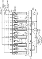
For example, shown in Fig. 1, Fig. 4, Fig. 6 etc., film formation device 1a possess be used for from move into take out of oral-lateral towards the inboard laterally to carry place carry the substrate S that puts on the platform 2 above for example 10 partition walls 41 of cutting apart of space.In addition, illustrate for ease, represented to be provided with the example of 10 partition walls 41, but the number of partition wall 41 is not limited to this.Each partition wall 41 for example is made up of the sheet material of metal flat linearity, and for example the length of its Width is longer than the minor face of substrate S.These partition walls 41 with the limit of above-mentioned Width with carry put the substrate S on the platform 2 long limit in laterally vertical mode in parallel to each other for example uniformly-spaced to dispose; Thus, be formed with the elongated space (the plasma span of stating after being equivalent to 401, exhaust space 402) of extending between 2 partition walls 41 that adjoin each other to the direction vertical with the long limit of substrate S.Each partition wall 41 is fixed on the top of container handling 10 through insulating element 31.
In addition, partition wall 41 is to form the for example mode in the slit about 1cm~5cm, the side extension downwards from above-mentioned top between the lower end of carrying the substrate S surface put on the platform 2 and partition wall 41.Thus, each space 401,402 that is surrounded by 2 partition walls 41 of adjacency is in the state that is interconnected through this slit.In addition, this slit is adjusted to moving into of 41 couples of substrate S of partition wall and takes out of the height that does not disturb in the path.
Be used to support from move into take out of oral-lateral several the 2nd with the 3rd partition wall 41, the 4th and the 5th partition wall 41, the 6th with the 7th partition wall 41, the 8th insulating element 31 with the 9th partition wall 41; Bearing of trend (along the direction vertical with the long limit of substrate S) along the space 401 between the partition wall that is formed at these adjacency 41 is formed with groove 31a.Like Fig. 4, shown in Figure 5, dispose the shower plate 32 that for example constitutes and possess a plurality of squit holes 321 by insulating element at the lower surface of these grooves 3a.
Be formed on the groove 31a of these insulating elements 31 and space that shower plate 32 is surrounded and be configured for H from the 1st reacting gas to the space 401 of its lower side that supply with as
2The 1st gas flow path 33.As shown in Figure 2, the 1st gas flow path 33 is connected with the 1st gas supply pipe 14 respectively at the side wall surface of container handling 10, can pass through the never illustrated H of the 1st gas supply pipe 14
2Supply source receives H
2(comprising the argon (Ar) that for example 10% plasma densification is used).In addition; In the 1st gas supply pipe 14, be provided with the not shown flow control division that constitutes by gas mass flow amount controller etc.; For example can in the scope of 1000cc/min~100000cc/min, regulate the H that supplies with to the 1st gas flow path 33 by standard state (25 ℃, 1 air pressure)
2Total amount.
The squit hole 321 of shower plate 32 is supplied with H equably with the space 401 to the below of the 1st gas flow path 33
2Mode be provided with.The 1st gas flow path 33, shower plate the 32, the 1st gas supply pipe 14 are equivalent to the 1st reaction gas supplying portion in this execution mode.
Next, to SiH
4Feed system describe.Each partition wall 41 its inside as shown in Figure 5 of the 2nd~the 9th become cavity.Be provided with a plurality of squit holes 412 at these partition walls 41 towards space 401 openings of the lower side of the 1st gas flow path of having narrated 33.Linearity ground is provided with these squit holes 412 along the lower surface in the bottom of this partition wall 41.Cavity in each partition wall 41 is configured for supplying with SiH through this squit hole 412 to the bottom in above-mentioned space 401
4The 2nd gas flow path 411.
As shown in Figure 2, each the 2nd gas flow path 411 is connected with the 2nd gas supply pipe 15 at the side wall surface of container handling 10, can pass through the never illustrated SiH of the 2nd gas supply pipe 15
4Supply source receives SiH
4Be provided with the not shown flow control division that constitutes by gas mass flow amount controller etc. at the 2nd gas supply pipe 15, for example can in the scope of 20cc/min~2000cc/min, regulate the SiH that supplies with to the 2nd gas flow path 411 by standard state (25 ℃, 1 air pressure)
4Total amount.The squit hole 412 of the 2nd gas flow path 411 sides also squit hole 321 with the shower plate of having narrated 32 is identical, supplies with SiH equably to the direction that is provided with squit hole 412
4Get final product.The 2nd gas flow path 411, squit hole the 412, the 2nd gas supply pipe 15 are equivalent to the 2nd reaction gas supplying portion of this execution mode.
Like Fig. 1 and shown in Figure 4, in the zone of carrying the circumference side put platform 2 upper surfaces, with around carry the substrate S that puts on the platform 2 and partition wall 41 around the periphery wall 22 of the mode side of being provided with tubular.As shown in Figure 4; Periphery wall 22 for example extends at above-below direction towards the top of container handling 10 from carrying the upper surface of putting platform 2; And take out of side and observe from moving into, front-back and about 4 faces of face cut exhaust outlet 23 as the vaccum exhaust outlet of this execution mode.
As shown in Figure 4, the periphery wall 22 in front and back respectively cut respectively one for example have with partition wall 41 almost with the exhaust outlet 23 of the broad of the width of degree.On the other hand; About periphery wall 22, be formed between the 1st and the 2nd partition wall 41, between the 3rd and the 4th partition wall 41, between the 5th and the 6th partition wall 41, between the 7th and the 8th partition wall 41, the 9th with the 10th partition wall 41 between 402 corresponding positions, space cut exhaust outlet 23.The exhaust outlet 23 of 4 periphery walls 22 all around all is formed on distance and carries high position about the upper surface 1cm~5cm put platform 2, promptly, compare high position with the lower end of partition wall 41.Here; The periphery wall 22 of taking out of mouthful 11 opposed fronts is as shown in Figure 1 with moving into; Moving axis 221 is taken out of the rotating mode of oral-lateral and is constituted towards moving into to rotate; Substrate S moves into when taking out of, and takes out of the oral-lateral rotation through making towards moving into, and does not disturb and make moving into of 22 couples of substrate S of periphery wall take out of the path.
And then, as shown in Figure 6, take out of the 3rd of oral-lateral from moving into, 4 partition walls 41 of the 4th, the 7th, the 8th are connected with high frequency electric source portion 51.For example with the 3rd with the 4th 2 as one group; Be connected with a high frequency electric source portion 51 at these; With the 7th with the 8th 2 partition walls 412 as 1 group, be connected with other high frequency electric source portion 51 at these, can apply the for example RF power of 100MHz, 5000W to these partition walls 41.On the other hand, take out of oral-lateral observation, the 1st, the 2nd, the 5th, the 6th, the 9th, the 10th these 6 partition wall 41 ground connection from moving into.
Through above formation, the 2nd with the 3rd partition wall 41, the 4th and the 5th partition wall 41, the 6th constitute the partition wall 41 that will be connected as negative electrode 43, with the partition wall 41 of ground connection parallel pole with the 7th partition wall 41, the 8th and the 9th partition wall 41 as anode 42 with high frequency electric source portion 51.And, if supply with H from the space 401 of the 1st gas flow path 33 between these partition walls 41 on one side
2Yi Bian, utilize high frequency electric source portion 51 to apply RF power, then the space between these parallel poles 401 forms capacitance coupling plasma, H
2By plasmaization.From this viewpoint, the space 401 that between the 2nd and 3 partition walls 41, between the 4th and the 5th partition wall 41, between the 6th and 7 partition walls 41, between the 8th and the 9th partition wall 41, forms is equivalent to the plasma span of this execution mode.In addition, the high frequency electric source portion 51 of parallel pole (negative electrode 43 and anode 42) and connection therewith is configured for activation H
2And the activation mechanism of generation plasma.
On the other hand, be connected with shared high frequency electric source portion 51 with the 8th partition wall 41 by each group with the 4th partition wall 41, the 7th, be equipotential, even space 402 supply gas between these partition walls 41 do not form plasma yet at the 3rd.Other the 1st with the 2nd partition wall 41, the 5th and the 6th partition wall 41, the 9th with the 10th partition wall 41 ground connection, be equipotential, therefore the space 402 between these partition walls 41 does not form plasma yet.And the periphery wall 22 in the left and right sides that is configured in these spaces 402 is provided with the exhaust outlet of having narrated 23, so the gas that flow in this space 402 passes through exhaust outlet 23, to the exhaust of the outside of periphery wall 22.From this viewpoint, the space 402 that between the 1st and the 2nd partition wall 41, between the 3rd and the 4th partition wall 41, between the 5th and the 6th partition wall 41, between the 7th and the 8th partition wall 41, between the 9th and the 10th partition wall 41, forms is equivalent to the exhaust space of this execution mode.Here, the partition wall 41 that forms each anode 42, negative electrode 43 is fixed on the top of container handling 10 through insulating element 31, so anode 42 and negative electrode 43 electric insulation except forming capacity coupled zone.
If summarize above formation, then as shown in Figure 6, in the inside of the related film formation device 1a of this execution mode,, alternately dispose the plasma span 401 and exhaust space 402 through the partition wall 41 that is provided with in parallel to each other.And; As narrating; Each plasma span 401, exhaust space 402 lower end through being formed on partition wall 41 with carry the slit of putting between the substrate S on the platform 2 and be communicated with, can be through this slit from the plasma span 401 towards exhaust space 402 gas bodies.
As shown in Figure 1, film formation device 1a possesses control part 5, and each formation portion of film formation device 1a is connected and Be Controlled with control part 5.Control part 5 for example is made up of the not shown computer that has possessed CPU and storage part; Record the program that realizes following content at storage part; With the effect of this film formation device 1a, promptly in container handling 10, move into substrate S, carry place carry the μ c-Si film of thickness that the substrate S that puts on the platform 2 forms regulation after relevant step (order) such as the related control of action till take out of group.This program for example is stored in the storage medium of hard disk, CD, magneto optical disk, storage card etc., is mounted to computer from there.
Next, the effect to the film formation device 1a of the formation that possesses above explanation describes.At first, if to remain on the state on the outside carrying arm 100, carrying comes substrate S, and then film formation device 1a opens and moves into the gate valve 12 of taking out of mouth 11, and, make periphery wall 22 rotations of front, to guarantee the path of moving into of substrate S.Then, make carrying arm 100 lower end that enters into partition wall 41 and the slit of carrying between the upper surface of putting platform 2,, then make carrying arm 100 drop to carry and put in the notch 20 of platform 2, substrate S is joined to year putting platform 2 if arrive the seated position of carrying of substrate S.
If accomplish the handing-over of substrate S, carrying arm 100 is returned to outside the container handling 10, closing gate valve 12, and make periphery wall 22 rotations, around periphery wall 22 encirclement substrate S.Carry out the vacuum exhaust in the container handling 10 simultaneously with this action, with being adjusted to for example 670Pa (5Torr) in the container handling 10, and utilize temperature adjustment portion 21 to carry out adjustment so that substrate S becomes for example 250 ℃.
Container handling 10 interior pressure are adjusted and the temperature adjustment of substrate S if accomplish, and then for example supplying with from the 1st gas flow path 33 to each plasma span 401, total amount is the H of 100000cc/min (standard state)
2, and from high frequency electric source portion 51 to each negative electrode 43 supply high frequency electric power, make H
2Plasmaization.On the other hand, for example supplying with from the 2nd gas flow path 411 to the lower area of the plasma span 401, total amount is the SiH of 500cc/min (standard state)
4
As Fig. 7 schematically shown in, in the plasma span 401, form the H that supplies with from the 1st gas flow path 33 sides
2Towards the sinking that lower side flows, this H
2With the electron collision of supplying with from parallel pole, thereby plasmaization forms spike.H
2Be the molecule that only constitutes, so shown in following (1) formula, only generate hydroperoxyl radical as spike from hydrogen plasma by 2 hydrogen atoms.
H
2+e
-→2H+e
- …(1)
On the other hand, supply with the SiH that flows out from the squit hole 412 of the 2nd gas flow path 411 to the bottom of the plasma span 401, the bottom of the plasma span 401 in this execution mode
4, with the next H of effluent from the upper reaches
2The air-flow of spike mix, effluent goes downwards.Therefore, SiH
4Hardly can plasmaization, do not comprise Si, SiH, SiH
2Etc. unwanted spike, even or comprise, also with less amount and H
2Spike mix, towards the substrate S of the below that is positioned at the plasma span 401 diffluence.
Its result supplies with as H to substrate S surface
2The H free radical and the SiH of spike
4Mist, in this mist, carry out the reaction shown in following (2) formula.
SiH
4+H→SiH
3+H
2 …(2)
Like this, the SiH of high concentration
3Be supplied to substrate S surface, by this SiH
3Form the μ c-Si film of high-quality on substrate S surface.
On the other hand, if in mist along with the process of time, the SiH that generates by above-mentioned (2) formula
3With the H radical reaction, then generate SiH successively again
2, SiH, Si, so, then become the reason that makes its membranous reduction if these spikes, sneak in the μ c-Si film as high order silanes, the particulate of its polymer.
; In the related film formation device 1a of this execution mode; The plasma span 401 is communicated with exhaust space 402 with slit between the substrate S through the lower end of partition wall 41, is provided with exhaust outlet 23 in high position, promptly high than the above-mentioned slit position, the lower end than the plasma span 401 of the periphery wall 22 on the two sides, the left and right sides of each exhaust space 402.And carry out vacuum exhaust in the container handling 10 all the time.Therefore; The aforementioned mist that has reduced the plasma span 401 arrives after the substrate S surface, Yi Bian flow through the surface of substrate S, Yi Bian through the slit between partition wall 41 and the substrate S; Flow into exhaust space 402;, make to flow to be changed to up thereafter, through exhaust outlet 23 to the exhaust promptly of the outside of periphery wall 22.
Here, in this execution mode, exhaust space 402 extends to the short side direction of substrate S, so for example compare to the situation of the long side direction diffluence of substrate S with mist, can shorten the average residence time on the substrate S.And, even be formed with under the situation of exhaust space 402 along the long side direction of substrate S, for example with the mist of supplying with to the middle section of substrate S flow through on the diagonal of substrate S situation relatively, also can shorten the residence time.Like this, exhaust space 402 has played the effect of shortening the residence time of the mist on the substrate S.
And, the effect of the exhaust outlet 23 of the mist that flows through substrate S surface through being arranged on periphery wall 22, its flow direction is changed to direction, so can further shorten the residence time of the lip-deep mist of substrate S.And, through the effect of these exhaust spaces 402, exhaust outlet 23, supply with the SiH of high concentration to substrate S surface
3, and can suppress the generation of unwanted spike, can access membranous good μ c-Si film.
Through the mechanism of above explanation, can play 2 effects having narrated, (1) suppresses SiH
4Plasmaization, make SiH
4With the H radical reaction, thereby suppress the generation of unwanted spike, supply with SiH to substrate S surface with high concentration
3, H free radical and SiH are promptly discharged from substrate S surface in (2)
4Mist, thereby suppress H free radical-SiH
4Between radical reaction excessively carried out, suppress the generation of unwanted spike.
So, only carry out film forming,, then stop H if obtain the μ c-Si film of desirable thickness to substrate S surface with the predefined time
2And SiH
4The applying and vacuum exhaust of supply, RF power, take out of substrate S with opposite action when utilizing carrying arm 100 to move into from container handling 10, accomplish a series of action.
The film formation device 1a related according to this execution mode has following effect.Promptly, in film formation device 1a, will carry through partition wall 41 and to place that to carry the superjacent air space put the substrate S on the platform 2 be the plasma span 401 and exhaust space 402 in horizontal partition, make H in the plasma span 401
2Activation generates plasma, and on the other hand, the lower side in the plasma span 401 is supplied with SiH
4, be supplied to the mist on the substrate S from exhaust space 402 discharges.Therefore, restraining, make SiH because of contacting with plasma under the state that promotes to decompose
4With according to H
2Spike (H free radical) reaction that gas generates, and can make SiH as purpose
3Near substrate S, exist, can form the μ c-Si film of high-quality with high concentration.
Be supplied to SiH here,
4The plasma span 401 in lower side be more to lean on the height and position of lower side than half of the plasma span 401; More preferably about 1/4th height and position from the lower end side of partition wall 41 to partition wall 41 just can be inhibited because of SiH
4Plasmaization and the such effect of the present invention of generation of the unwanted spike that causes.
In addition, be not limited to SiH
4Be supplied to the situation of the lower side of the plasma span 401, also can be supplied to than the plasma span 401 and more lean on lower side.Under this situation, for example also squit hole 412 can be set, discharge SiH towards substrate S in the lower surface of partition wall 41
4, also can be to supply with SiH in the lower position configuration of the plasma span 401
4The pipe arrangement of special use, supply with SiH from the squit hole 412 that is arranged on this pipe arrangement
4Formation.
< the 2nd execution mode >
Next, the 2nd execution mode is described.
In above-mentioned the 1st execution mode; Periphery wall 22 on every side through being arranged on substrate S is discharged the mist that is supplied to substrate S to a side; But be not limited thereto; In this execution mode, for example illustrate and exhaust line is set at the top of container handling, discharge the example of above-mentioned mist to upper side.Fig. 8~10 explanations are towards the formation of the related film formation device 1b of the 2nd execution mode of the mist on the top side discharge supplying substrate S surface of container handling 10.Should explain, this execution mode and after in the later execution mode of the 3rd execution mode stated, to having possessed the inscape mark symbol identical with film formation device 1a identical function with the 1st execution mode.
The related film formation device 1b of this execution mode puts different with the related film formation device 1a of the 1st execution mode at following these: do not possess to surround to carry to place and carry the periphery wall 22 of putting the substrate S on the platform 2; Exhaust line 13 is arranged on the top of container handling 10, is communicated with each exhaust space 402 and the set exhaust portion 16 at mist interflow before exhaust line 13 exhausts being provided with above the 1st gas flow path 33.
In this execution mode, dispose insulating element 31 with the mode of the upper face side that covers 2 partition walls 41 that shower plate 32 is set between it, in the space that surrounds by these 2 partition walls 41, shower plate 32, insulating element 31, form the 1st gas flow path 33.In addition, the handing-over of substrate S is to use lifter pin 24 to carry out.Among Fig. 8, symbol 25 is the bellowss that are provided with the mode of surrounding lifter pin 24 in order to keep container handling 10 interior vacuum environments, the 26th, and the elevating mechanism that lifter pin 24 is gone up and down.
In the related film formation device 1b of this execution mode; For example each partition wall 41 is rectangular side's barrel shape by the cross section of observing from upper face side as shown in Figure 9 parts 413 constitute, these side's cartridge units 413 with the state configuration of the side wall surface that is fixed in container handling 10 in container handling 10.And; To take out of oral-lateral and observe the the 1st, the 3rd, the 5th square cartridge unit 413 and fix from moving into the mode that is electrically connected with the container handling 10 of ground connection; On the other hand, the 2nd, the 4th square cartridge unit 413 is fixed on container handling 10 through insulating element 17, these side's cartridge units 413 are connected with high frequency electric source portion 51; Thereby the film formation device 1a related with the 1st execution mode shown in Figure 6 is identical, alternately the configuring plasma span 401, exhaust space 402 (with reference to Fig. 9).
In this film formation device 1b, also supply with H to the plasma span 401
2Generate plasma, from this plasma H free radical that obtains and the SiH that is supplied to the lower side of the plasma span 401
4Mix, and can be to the SiH of substrate S supply high concentration
3, the related film formation device 1a of this point and the 1st execution mode is identical.Shown in figure 10; In the related film formation device 1b of this example; While flow through mist that substrate S surface flows into to exhaust space 402 towards gather exhaust portion 16 sides in exhaust space 402 to the upper side diffluence, so the residence time of the mist among the substrate S become shorter.Its result, can suppress based on radical reaction generate unwanted spike etc., form the μ c-Si film of high-quality.
Here; If because with the exhaust of mist towards the top side of container handling 10; As long as exhaust space 402 is communicated with the top side of discharging mist, so for example also can be shown in Figure 11, shape ground disposes partition wall 41 with one heart; Between the parallel pole that forms by these partition walls 41 (anode 42, negative electrode 43), form the formation of plasma.
< the 3rd execution mode >
Next, the 3rd execution mode is described.
In this execution mode, show the example of microwave antenna unit as activation mechanism is set in the top position of the plasma span.Figure 12~16 explanations are provided with the formation of microwave antenna unit 6 as the related film formation device 1c of the 3rd execution mode of activation mechanism in the top position of the plasma span 401.
The film formation device 1c that this execution mode is related; Like Figure 12, shown in Figure 13; Through top board 181 container handling 10 is divided into 2 spaces up and down, identical with the film formation device 1a that has narrated in the space of lower side, platform 2 is put in carrying of placement substrate S; On the other hand, the space of upper side becomes the incorporating section 18 of taking in a plurality of microwave antenna units 6.
Shown in figure 13, in incorporating section 18, for example be 3 row at left and right directions, fore-and-aft direction for example is that each intersection point of the matrix of 5 row is provided with microwave antenna unit 6, on top board 181, adds up to 15 microwave antenna units 6 to be island ground and disposes dispersedly.And, be useful on the partition wall 41 that forms the plasma span 401 in the spatial configuration of lower side across the top board 181 of these each microwave antenna units 6.
The related partition wall 41 of this example is Figure 13, shown in Figure 14 for example, forms drum with the mode around the space of the lower side of each microwave antenna unit 6.Its result is provided with the partition wall 41 that adds up to 15 drums with being island in carrying the space of putting substrate S, the outside that the inboard of these partition walls 41 becomes the plasma span 401, partition wall 41 becomes exhaust space 402.
Next, with reference to Figure 15, the formation of microwave antenna unit 6 is described.Microwave antenna unit 6 is made up of tuner 61 and antenna part 62, and these tuners 61 are taken in this order from upside in the for example metal framework 600 of the outer conductors of cylindrical shape and formation coaxitron with antenna part 62.The antenna part 62 of downside possesses discoideus planar slot antenna plate 621; Be located at the upside of this planar slot antenna plate 621; And the wavelength that is used for shortening the microwave of vacuum environment adjust plasma density ring-type stagnant parts for wave 622, be located at the downside of planar slot antenna plate 621, and the top board 623 that constitutes by dielectric members.
In planar slot antenna plate 621, flat shape is that 2 circular-arc grooves 624 form with opposed mode.And, the central portion on planar slot antenna plate 621, the mode of extending towards the top with the central portion from the parts for wave 622 that stagnates is connected with the metal bar 64 of the inner conductor that forms coaxitron.Shown in figure 15, each microwave antenna unit 6 is connected in parallel through shared microwave efferent 63 and amplifier portion 631, and top board 623 plays the microwave from this microwave efferent output is imported the effect in the plasma span 401.
In tuner 61, be provided with ring-type and for example 2 pellets 611 that are made up of dielectric of being provided with discretely at above-below direction, the metal bar of having narrated 64 connects the central part of these pellets 611 at above-below direction.Each pellet 611 is connected with drive division 613 through the arm 612 that extends laterally towards the peripheral direction of framework 600, thereby constitutes with the mode of free lifting respectively.(L1 is L2) so that the impedance during from the microwave antenna unit 6 in microwave efferent 63 observation downstreams is for example 50 Ω to adjust the height and position of each pellet 611.In addition, tuner 61 closely disposes with the planar slot antenna plate of having narrated 621, constitutes the lumped circuit in 1 wavelength that is present in microwave, as resonator performance function.
Upper end at the metal bar 64 that connects tuner 61 is provided with the power supply excitation plate 65 that is used to carry out non-contact power.This power supply excitation plate 65 possesses the dielectric plate 651 that is made up of printed circuit wiring etc.; The dielectric members 652 that is provided with in the form of a ring at the downside of this dielectric plate 651.Rear side at dielectric plate 651 is formed with by the central part that clips dielectric plate 651, diametrically opposedly extends with putting, and the microstrip line 653 that constitutes of leading section 2 conductors separated from one another.
End at the microstrip line 653 of the lateral circle surface that is positioned at dielectric plate 651 is separately installed with connector 654, and these connectors 654 are connected with the amplifier portion of having narrated 631 respectively.Therefore, supply with microwave to tuner 61 through 2 connector 654 electric power synthetic (space is synthetic).In addition, 655 are the reflecting plates that are used for microwave reflection among the figure.
Be provided with at the lower surface of dielectric members 652 and for example carried out copper facing etc., and flat shape is the discoideus slot antenna 656 that 2 circular-arc grooves 657 form with opposed mode.This microwave antenna unit 6 for example is that (λ g: the mode wavelength in pipe of microwave) forms 1/2 * λ g with the length dimension of groove 657.This dielectric members 652 as resonator performance function, is provided with center conductor 658 at central part with the mode that connects dielectric members 652 at above-below direction, to connect the lower face side and the slot antenna 656 of dielectric plate 651 with slot antenna 656.
If the microwave of supplying with the regulation power from the microwave efferent 63 of the microwave antenna unit 6 that possessed said formation is the microwave of frequency 2.45GHz, power 2000W~10000W for example; Then microwave is after amplifier 631 is exaggerated; Through not shown distributor, be assigned to each microwave antenna unit 6.And, in each microwave antenna unit 6,, be supplied to the plasma span 401 through planar slot antenna 621 through behind the synthetic microwave that amplifies of 2 microstrip lines, 653 inputs.
Its result, shown in figure 16, supply with the H in the plasma span 401
2Through the microwave of supplying with from microwave antenna unit 6, plasmaization generates the H free radical as spike, with the SiH of the lower side that is supplied to the plasma span 401
4Reaction can be to the SiH of substrate S surface supply high concentration
3And, these H free radical and SiH
4Mist flow into the space (exhaust space 402) of outer circumferential side of the partition wall 41 of drum, this exhaust space 402 in to the side effluent, through the slit between top board 181 and the periphery wall 22 to the discharge of the outside of periphery wall 22.From this viewpoint, the slit between top board 181 and the periphery wall 22 is equivalent to the vaccum exhaust outlet of this execution mode.Here, the microwave antenna unit 6 that is arranged at the related film formation device 1c of this execution mode is not limited to microwave antenna unit shown in Figure 15, also can use the common waveguide that is connected with microwave efferent 63.
< the 4th execution mode >
Next, the 4th execution mode is described.
In above-mentioned the 3rd execution mode; The upper side that shows in the plasma span is provided with the example of microwave antenna unit 6 as activation mechanism; But be not limited thereto; In this execution mode, the upper side that is illustrated in the plasma span is provided with the example of ICP (Inductively CoupledPlasma) antenna as activation mechanism.Figure 17~20 explanations are provided with the formation of ICP antenna 7 as the related film formation device 1d of the 4th execution mode of activation mechanism at the upper side of the plasma span 401.
The film formation device 1d that this execution mode is related; Figure 17, shown in Figure 180 for example, in the incorporating section of being divided by the top board above each plasma span 401 181 18, be provided with for example straight bar-shaped ICP antenna 7 this point that the direction of extending along this plasma span 401 extends with each partition wall 41 is connected with high frequency electric source portion 51 or ground connection to form the related film formation device 1a of the 1st execution mode of parallel pole different.In addition, shown in figure 19, the direction of on top board 181, extending along the plasma span 401 is equipped with the 1st gas flow path 33, carries out H through the 1st gas flow path 33
2The supply this point supply with H with the space that is the 1st gas flow path 33 of top through being configured in the plasma span 401
2The film formation device 1a that has narrated different.
The film formation device 1d related according to this execution mode; In incorporating section 18, dispose 4 ICP antennas 7 along each plasma span 401; These ICP antennas 7 one distolateral with supply with for example 13.56MHz; The shared high frequency electric source portion 51 of the electric power of 5000W is connected in parallel, on the other hand, and the other end side joint ground of each ICP antenna 7.And apply RF power to ICP antenna 7 from high frequency electric source portion 51, thus in the plasma span 401, form induction field, shown in figure 20, the H that supplies with from the 1st gas flow path 33
2Inductively coupled plasmaization, and, to the underfeed SiH of partition wall 41
4Thereby, can be to the SiH of substrate S surface supply high concentration
3
In addition; Along the mist of exhaust space 402 to the side directed inflow exhaust space 402 in the side of container handling 10; And, discharge mist through the exhaust outlet 23 that is arranged on the position higher, thereby make the flow direction of this gas be changed to upper side towards substrate S than the lower end of partition wall 41; Can shorten the residence time of the lip-deep mist of substrate S, form the membranous μ c-Si film of high-quality.
The ICP antenna 7 of the film formation device 1d that this execution mode is related is not limited to form straight bar-shaped situation; For example each ICP antenna 7 is formed the toroidal that a part is cut; Also can as the related film formation device 1c of the 3rd execution mode, on top board 181, be the ICP antenna 7 of island ground this toroidal of decentralized configuration.Under this situation, an end of the ICP antenna 7 of the toroidal of incision is connected with high frequency electric source portion 51, and other end ground connection, thereby can form inductively coupled plasma in the lower side of this toroidal.Therefore, in such example, the mode that can certainly form the zone with the plasma of the lower side of surrounding ICP antenna 7 is provided with the partition wall 41 of drum.
In addition; In the related film formation device 1c of above-mentioned the 3rd execution mode; Microwave antenna unit 6 is the island decentralized configuration on top board 181, but is not limited thereto, also can be identical with the related film formation device 1d of this execution mode; Uniformly-spaced dispose a plurality of flat partition walls 41 at fore-and-aft direction, for example along a plurality of microwave antenna units 6 of the plasma span of extending 401 configurations to the direction vertical with the long limit of substrate S.
In the related film formation device 1a of the 1st, the 3rd, the 4th execution mode, 1c, 1d; Periphery wall 22 is set around substrate S; With the vaccum exhaust outlet of the slit between the exhaust that is formed on this periphery wall 22 23, periphery wall 22 and the top board 181, put the formation that periphery wall 22 is not set on the platform 2 but also can be employed in to carry as the gas on the substrate S.Under this situation, the connecting portion that is connected with the exhaust line 13 of the side wall surface that is arranged on container handling 10 becomes vaccum exhaust outlet.
< the 5th execution mode >
Next, the 5th execution mode is described.
Figure 21, Figure 22 explain the formation of the film formation device 1e that the 5th execution mode is related.The related film formation device 1e of this execution mode has common characteristic in alternately the configuring plasma span 401 and exhaust space 402 this point with the related film formation device 1b of the 2nd execution mode that uses Fig. 8~10 explanations.On the other hand, the related film formation device 1e of this example the space that is formed between opposed 2 partition walls 41 is passed in time be changed to the plasma span 401 → exhaust space 402 → plasma span 401 → ... the related film formation device 1b of this point and the 2nd execution mode of having narrated is different.
Like Figure 21, shown in Figure 22; Film formation device 1e for example possess towards figure from the left side towards the right side horizontal partition carry place carry the substrate S that puts platform 2 above a plurality of partition walls 41 in space, these partition walls 41 for example are maintained on the shared top board 181 that is made up of insulating element.In Figure 21, Figure 22,, show the example that is provided with 6 partition walls 41, but the number of partition wall 41 is not limited to this for convenient diagram.
In the inside of each partition wall 41, be formed with the inside panel 414 that extends through along the vertical direction, be divided into 2 spaces on left side and right side, each space is configured for supplying with SiH through squit hole 412 to the for example bottom of partition wall 41
4The 2nd gas flow path 411.In Figure 21, the example shown in Figure 22; Show foremost and the example that only forms one the 2nd gas flow path 411 in the partition wall 41 of rearmost end respectively; Certainly these partition walls 41 also can be identical with other partition wall 41, and 2 the 2nd gas flow paths 411 respectively are set.
Shown in figure 22, the 2nd gas flow path 411 that is formed in the partition wall 41 passes through the 2nd gas supply pipe 15a, 15b and SiH
4Supply source 150 connects.And 2 the 2nd gas flow paths 411 in each partition wall 41 connect with the 2nd gas supply pipe 15a, the 15b of different system respectively.In this execution mode, be connected with the 2nd gas flow path 411 on the right side of the 2nd partition wall 41 from the left side at the 2nd gas supply pipe 15a of side's side, from the left side left side of the 3rd partition wall 41 the 2nd gas flow path 411, from the left side left side of the 3rd partition wall 41 the 2nd gas flow path 411, from the left side right side of the 4th partition wall 41 the 2nd gas flow path 411 and from the left side the 2nd gas flow path 411 in the left side of the 5th partition wall 41.In addition, be connected with the 2nd gas flow path 411 of the 1st partition wall 41 at the gas supply pipe 15b of the opposing party's side from the left side, from a left side left side of the 2nd partition wall 41 the 2nd gas flow path 411, from the left side right side of the 3rd partition wall 41 the 2nd gas flow path 411, from the left side left side of the 4th partition wall 41 the 2nd gas flow path 411, from the left side right side of the 5th partition wall 41 the 2nd gas flow path 411 and from the left side the 2nd gas flow path 411 of the 6th partition wall 41.
In addition, in the top board 181, the almost middle position between opposed 2 partition wall 41 is formed with and these partition walls 41 parallel the 1st gas flow paths 33 that extend, can be through supplying with H in the space of squit hole 321 before and after being clipped by 2 partition walls 41
2These the 1st gas flow paths 33 are also through the 1st gas supply pipe 14a, 14b and H
2Supply source 140 connects, but the 1st gas supply pipe 14a, the 14b connection of each the 1st gas flow path 33 and different system.In this execution mode; Be arranged on towards figure from the 2nd of left-hand digit with the 3rd partition wall 41 between, the 4th with the 5th partition wall 41 between the 1st gas flow path 33 be connected with the 1st gas supply pipe 14a, be arranged on the 1st with the 2nd partition wall 41 between, the 3rd with the 4th partition wall between, the 5th with the 6th partition wall 41 between the 1st gas flow path 33 be connected with the 1st gas supply pipe 14b.In addition, the squit hole 321 that is arranged on the 1st gas flow path 33 can be put the substrate S on the platform 2 towards being carried to place to carry towards the lower side opening, in the space that is formed between the opposed partition wall 41, supplies with H
2
At the 2nd gas supply pipe 15a, 15b, the 1st gas supply pipe 14a, 14b are respectively arranged with open and close valve V1~V4, can carry out SiH by each system
4, H
2Confession disconnected.These open and close valves V1~V4 constitutes the gas of this execution mode and supplies with switching part.In the following explanation, supply pipe 15a, the 14a that will mark " a " symbol are called 1 system, the supply pipe 15b of mark " b " symbol, and 14b is called 2 systems, distinguishes each other.
Next, gas extraction system is described.
Next, electric power system is described.
Among the related film formation device 1e of this execution mode, be connected with high frequency electric source portion 51 all the time from the 1st of left-hand digit and the 5th partition wall 41 towards figure, on the other hand, the 3rd partition wall 41 be ground connection all the time.And the 2nd, the 4th, the 6th partition wall 41 switches to linking objective and the power supply terminal side of high frequency electric source portion 51 and any side in the ground connection side through as the switch portion 52a~52c that connects switching part.The linking objective of switch portion 52a shown in Figure 22~52c is that contact 521 is high frequency electric source portion 51 sides, and contact 522 is the ground connection side.
In having possessed the film formation device 1e of said formation, shown in Figure 23 A, switch portion 52a, 52c are connected with the contact 521 of high frequency electric source portion 51 sides, on the other hand, switch portion 52b is connected with the contact 522 of ground connection side.Thus, to the 1st, the 2nd, the 5th, the 6th partition wall 41 supply high frequency electric power, in addition, the 3rd, the 4th partition wall 41 are in the state of ground connection.
And if a side of opposed partition wall 41 is connected with high frequency electric source portion 51, the opposing party's ground connection then forms above-mentioned side's side as negative electrode 43, with the parallel pole of the opposing party's side as anode 42.Therefore, if supply with H from the space of the 1st gas flow path 33 between parallel pole
2, then this space becomes and makes H
2The plasma span 401 of plasmaization.In the example shown in Figure 23 A, between the 2nd and the 3rd partition wall 41, become the plasma span 401 between the 4th and the 5th partition wall 41.
Relative therewith, the 1st all is connected with high frequency electric source portion 51 with the 6th partition wall 41 with the 2nd partition wall 41 and the 5th, in addition, the 3rd with the 4th partition wall 41 ground connection.Therefore these the 1st with the 2nd partition wall 41 between, space between the 3rd and the 4th partition wall 41, between the 5th and the 6th partition wall 41 is equipotential, even supply H
2Do not form plasma yet.
At this moment; If, then in the plasma span 401, supply with H towards lower side from the 1st gas flow path 33 with the valve V3 of the 1st gas supply pipe 14a that synchronously opens 1 system side by the selection of the linking objective of switch portion 52a~52c and the valve V1 (being designated as " O " among Figure 23 A) of the 2nd gas supply pipe 15a
2, make this H
2Plasmaization generates the H free radical.Supply with SiH to the lower side of this plasma span 401 then
4Thereby, mix H free radical and SiH4, can supply with the required SiH of growth of μ c-Si film with high concentration to the surface of substrate S
3
The valve V4 of the 1st gas supply pipe 14b of 2 system side that are connected with the space that does not form plasma on the other hand, and the valve V2 of the 2nd gas supply pipe 15b close (being designated as " S " among Figure 23 A).And carry out exhaust to exhaust line, thereby the H free radical and the SiH that contact with substrate S in the lower side of the plasma span 401 through set exhaust portion 16
4Mist change to flow to towards upper side, flow in the set exhaust portion 16 through steam vent 182 (and gas entrance hole 161) and be deflated.
Therefore, opposed partition wall 41 is equipotential, does not supply with H from the 1st, the 2nd gas flow path 33,411
2, SiH
4The space be configured for discharging the exhaust space 402 of the mist on the surface that is fed into substrate S.In this execution mode; The mist on the surface of supplying substrate S towards the set exhaust portion 16 in exhaust space 402 to the upper side diffluence; So identical with execution mode before, the residence time of the mist on the substrate S shortens, can form the μ c-Si film of high-quality.
Here, identical with exhaust space 402, each plasma span 401 also is connected with set exhaust portion 16 through steam vent 182, so worry from the H of the 1st gas flow path 33 supplies
2Flow to set exhaust portion side, carry the surface of putting the substrate S on the platform 2 and can not arrive.Yet, as narrating, so that the squit hole 321 of the 1st gas flow path 33 towards the lower side perforate, is discharged H in the plasma span 401
2Mode constitute, thereby can make the H that supplies with from squit hole 321
2Major part ride over towards the flowing of lower direction, arrive substrate S, this situation is confirmed through the simulation of using the fluid simulation device.
Like this; If under the state shown in Figure 23 A; For example with during the several seconds~several branches during so predefined time carry out film forming; Then shown in Figure 23 B,, contact 521 ways of connecting of switch portion 52b and high frequency electric source portion 51 sides are switched so that switch portion 52a, 52c are connected with the contact 522 of ground connection side.Its result; Through the 1st with the 2nd partition wall 41, the 3rd and the 4th partition wall 41, the 5th form parallel pole respectively with the 6th partition wall 41; On the other hand, between the 2nd and the 3rd partition wall 41, be equipotential between the 4th and the 5th partition wall 41.
So; Through synchronously opening the valve V4 of the 1st gas supply pipe 14b of 2 system side that are connected with the space that forms parallel pole, the valve V2 of the 2nd gas supply pipe 15b with the change action of switch portion 52a~52c; Close the valve V3 of the 1st gas supply pipe 14a of 1 system side, the valve V1 of the 2nd gas supply pipe 15a; And can the space that be formed with parallel pole be switched to the plasma span 401, equipotential space is switched to exhaust space 402.In addition, the valve that is opened among Figure 23 B also is expressed as " O ", and pent valve is expressed as " S ".
Its result switches to exhaust space 402 in the zone that forms space 401 as plasma under the state of Figure 23 A under the state of Figure 23 B, on the contrary, switch to the plasma span 401 as the zone of exhaust space 401 at Figure 23 B at Figure 23 A.So, through the state shown in the state shown in Figure 23 A and Figure 23 B repeatedly alternately, and switch the plasma span 401 and exhaust space 402 by pre-set time interval, can realize supply with the uniform mist of time average.Thus, can form thickness and membranous μ c-Si film more uniformly on the surface of substrate S.
Like this, switching the method that the mode of the plasma span 401 and exhaust space 402 constitutes with in time passing is not limited to supply with H from the 1st gas flow path 33 to the zone of the upper side of the plasma span 401
2, with SiH
4From zone and the H of the 2nd gas flow path 411 to the lower side of the plasma span 401
2The application of the example of separately supplying with.For example shown in figure 24, can in each partition wall 41, the 2nd gas flow path be set yet, the 1st gas flow path 33 in being arranged on top board 181 is supplied with H from mist supply pipe 17a, the 17b of 2 systems
2With SiH
4Mist.In this case; Through switch portion 52a~52b and be set at the last valve V1 of mist supply pipe 17a, 17b, the switching of V2; Identical with the example shown in Figure 23 A, Figure 23 B; Between opposed partition wall 41, switch and form the plasma span 401 and exhaust space 402, and can supply with the uniform mist of time average to the surface of substrate S.
In addition, the method as the plasma span 401 between the opposed partition wall 41 is not limited to be connected as negative electrode 43 with high frequency electric source portion 51 through a side who makes partition wall 41, the opposing party's ground connection is as anode 42, and the method for formation parallel pole.For example shown in figure 25, also can in the set exhaust portion 16 above the top board 181, wait configuration ICP antenna 7a, 7b., utilize the not shown switch portion of formation connection switching part etc. here, can switch the ground supply capability from 51 pairs of ICP antennas 7a of high frequency electric source portion and ICP antenna 7b.And, supply with H from the 1st gas flow path 33 and the 2nd gas flow path 441 because of the supply capability to ICP antenna 7a, 7b forms the zone of induction field
2And SiH
4Thereby, can with should the zone as the plasma span 401.On the other hand, at the ICP antenna 7b of supply capability not, H is not carried out in the space of the lower side of 7a
2, SiH
4Supply, thereby this space is played a role as exhaust space 402.And passing in time alternately carries out the formation of these plasma spans 401 and the formation of exhaust space 402, thereby can carry out and the identical action of film formation device 1e shown in Figure 23 A, Figure 23 B.
In addition, in order to form the plasma span 401, the activation mechanism that is arranged on the top of opposed partition wall 41 is not limited to situation about being made up of ICP antenna 7a, 7b and high frequency electric source portion 51.For example also can dispose the row that a plurality of microwave antenna units of having narrated 6 form microwave antenna unit 6 along the space line shape ground that is formed between the opposed partition wall 41; Utilize not shown switch portion (connection switching part) etc. to switch the microwave of carrying out as the microwave efferent 63 of power supply unit and supply with, thereby exchange the position of the plasma span 401 and exhaust space 402 by each row.
More than explanation, in time passing alternately forms among the film formation device 1e of the plasma span 401 and the type of exhaust space 402 between opposed 2 partition walls 41, is not limited to gather exhaust portion 16 is discharged mist towards single cavity shown in Figure 21 example.For example also can the division wall be set accordingly with the position that is provided with partition wall 41 in set exhaust portion 16 divides in this set exhaust portion 16.And can stop exhaust with set exhaust portion 16 for the top of the plasma span 401, only carry out the exhaust position that switches set exhaust portion 16 from exhaust space 402 to the mode of the exhaust of set exhaust portion 16.
In addition, the exhaust of the mist that carries out from exhaust space 402 shown in Figure 23 A, Figure 23 B, is not limited to the situation of carrying out from the upper side of exhaust space 402, for example also can be identical with example shown in Figure 4, implement from the side of exhaust space 402.
And the partition wall 41 that forms parallel pole is not limited to side's side and is connected the situation on the opposing party's side joint ground with high frequency electric source portion 51.For example also can be with respect to the RF power that applies to side's side, the mode that applies the RF power of phasing back to the partition wall 41 of the opposing party's side constitutes parallel pole.
And the state shown in Figure 23 A (the 1st state) is preferably carried out the identical time with the time of implementation of the state shown in Figure 23 B (the 2nd state), but this condition not necessarily.Even under mutual condition of different of the time of implementation of the 1st, the 2nd state; Compare with the situation that the position of the plasma span 401 and exhaust space 402 is fixed; The departing from of supply condition of the mist when observing can be improved, thickness, membranous uniformity can be improved with time average.
No matter above which execution mode; All the superjacent air space with substrate is the plasma span and exhaust space through partition wall in horizontal partition; Make the 1st reacting gas activation generate plasma in the plasma span; On the other hand, to more supplying with the 2nd reacting gas, discharge the gas on the substrate from exhaust space by lower side than the lower side in the plasma span or this plasma span.Therefore restrain because of with state that contacting of plasma promotes to decompose under, make the 2nd reacting gas and the spike reaction that generates according to the 1st reacting gas, and can make the film forming kind as purpose near substrate, exist with high concentration.
In addition, the present invention is not limited to be applicable to and utilizes H
2With SiH
4The situation of film forming of Si film.For example also can be applicable to the 1st reacting gas as H
2, with the 2nd reacting gas as SiH
4Silicon compound gas in addition, for example SiH
2Cl
2, the situation of formation micro-crystallization Si.
Claims (12)
1. a film formation device makes multiple reacting gas reaction in the container handling of sealing, on substrate, forms film, and this film formation device possesses:
Carry and to put platform, it is set in the said container handling, and is used for carrying and puts substrate;
Partition wall; It will carry the superjacent air space that places the substrate of putting platform in said year downwards is that the mode of the plasma span and exhaust space is provided with to extend from the top of said container handling in horizontal partition, between its lower end and the substrate put on the platform in said year, is formed for from the slit of the said plasma span to the exhaust space flowing gas;
The 1st reaction gas supplying portion, it is used for supplying with the 1st reacting gas to the said plasma span;
Activation mechanism, it is used for making the 1st reacting gas activation that is supplied to the said plasma span and generates plasma;
The 2nd reaction gas supplying portion, its lower side that is used in the said plasma span perhaps more leans on lower side to supply with the spike reaction of the 1st reacting gas film forming the 2nd reacting gas on substrate than this plasma span; And
Vaccum exhaust outlet, it is used for said exhaust space is carried out exhaust.
2. film formation device according to claim 1 is characterized in that,
Said vaccum exhaust outlet is formed on the position higher than the lower end of said partition wall.
3. film formation device according to claim 1 is characterized in that,
Said activation mechanism has:
Constitute the anode and the negative electrode of parallel pole, this parallel pole is used for generating capacitance coupling plasma in the plasma span; And
Between said anode and said negative electrode, apply the high frequency electric source portion of RF power.
4. film formation device according to claim 1 is characterized in that,
Said activation mechanism has the antenna that is set at the top of the said plasma span in order to generate inductively coupled plasma or microwave plasma.
5. film formation device according to claim 1 is characterized in that,
Possess a plurality of said partition walls, these a plurality of partition walls are provided with in parallel to each other, come alternately to dispose a plurality of plasma spans and a plurality of exhaust space through these a plurality of partition walls.
6. film formation device according to claim 5 is characterized in that,
Said partition wall is in laterally linearity ground extension.
7. film formation device according to claim 5 is characterized in that,
Said activation mechanism has:
Be configured for generating the anode and the negative electrode of the parallel pole of capacitance coupling plasma, this anode and negative electrode are set at across said each plasma span and a side and the opposing party of mutual opposed partition wall; And
Between said anode and said negative electrode, apply the high frequency electric source portion of RF power.
8. film formation device according to claim 5 is characterized in that,
Said activation mechanism has:
A plurality of electrodes, it is arranged at said a plurality of partition walls each respectively, and the said electrode that is set on the mutual opposed partition wall is the pair of electrodes that is configured for generating in the plasma span parallel pole of capacitance coupling plasma each other;
High frequency electric source portion, it applies RF power between said pair of electrodes; And
Connect switching part, the mode that it exchanges the position of the said plasma span and exhaust space with pre-set time interval, the electrode of the said parallel pole of switching formation is connected with the power supply terminal of high frequency electric source portion.
9. film formation device according to claim 8 is characterized in that,
Also possess gas and supply with switching part; This gas is supplied with switching part does not offer said exhaust space according to said the 1st reacting gas and the 2nd reacting gas are offered said plasma space mode, the supply of synchronously switching gas with the said change action that is connected switching part.
10. film formation device according to claim 1 is characterized in that,
Said partition wall forms tubular with the mode of surrounding the plasma span, and the partition wall of this tubular be provided with being island a plurality of,
Said activation mechanism has each the antenna element of top that is arranged on the said plasma span in order to generate inductively coupled plasma or microwave plasma.
11. film formation device according to claim 1 is characterized in that,
Said vaccum exhaust outlet is formed on the sidewall of container handling.
12. film formation device according to claim 1 is characterized in that,
The 1st reacting gas is a hydrogen, and the 2nd reacting gas is a silicon compound gas.
Applications Claiming Priority (5)
| Application Number | Priority Date | Filing Date | Title |
|---|---|---|---|
| JP2009-215851 | 2009-09-17 | ||
| JP2009215851 | 2009-09-17 | ||
| JP2010161955A JP5648349B2 (en) | 2009-09-17 | 2010-07-16 | Deposition equipment |
| JP2010-161955 | 2010-07-16 | ||
| PCT/JP2010/064707 WO2011033927A1 (en) | 2009-09-17 | 2010-08-30 | Film formation apparatus |
Publications (1)
| Publication Number | Publication Date |
|---|---|
| CN102498546A true CN102498546A (en) | 2012-06-13 |
Family
ID=43758536
Family Applications (1)
| Application Number | Title | Priority Date | Filing Date |
|---|---|---|---|
| CN2010800411155A Pending CN102498546A (en) | 2009-09-17 | 2010-08-30 | Film formation apparatus |
Country Status (6)
| Country | Link |
|---|---|
| US (1) | US20120247390A1 (en) |
| EP (1) | EP2479780A4 (en) |
| JP (1) | JP5648349B2 (en) |
| KR (1) | KR101361955B1 (en) |
| CN (1) | CN102498546A (en) |
| WO (1) | WO2011033927A1 (en) |
Cited By (5)
| Publication number | Priority date | Publication date | Assignee | Title |
|---|---|---|---|---|
| CN104112639A (en) * | 2013-04-22 | 2014-10-22 | 中微半导体设备(上海)有限公司 | Plasma reaction chamber for realizing fast reaction gas switching and method thereof |
| CN105244250A (en) * | 2014-07-03 | 2016-01-13 | 斯克林集团公司 | Etching apparatus and etching method |
| CN107230608A (en) * | 2016-03-25 | 2017-10-03 | 芝浦机械电子装置株式会社 | Plasma Processing Apparatus |
| CN111349912A (en) * | 2018-12-21 | 2020-06-30 | 富士施乐株式会社 | Film forming apparatus and film forming method |
| CN112334599A (en) * | 2018-06-25 | 2021-02-05 | 东芝三菱电机产业系统株式会社 | Active gas generating apparatus and film forming apparatus |
Families Citing this family (129)
| Publication number | Priority date | Publication date | Assignee | Title |
|---|---|---|---|---|
| US10049859B2 (en) * | 2009-07-08 | 2018-08-14 | Aixtron Se | Plasma generating units for processing a substrate |
| US9324576B2 (en) | 2010-05-27 | 2016-04-26 | Applied Materials, Inc. | Selective etch for silicon films |
| KR101693673B1 (en) * | 2010-06-23 | 2017-01-09 | 주성엔지니어링(주) | Gas distributing means and Apparatus for treating substrate including the same |
| US10283321B2 (en) | 2011-01-18 | 2019-05-07 | Applied Materials, Inc. | Semiconductor processing system and methods using capacitively coupled plasma |
| US8999856B2 (en) | 2011-03-14 | 2015-04-07 | Applied Materials, Inc. | Methods for etch of sin films |
| US9064815B2 (en) | 2011-03-14 | 2015-06-23 | Applied Materials, Inc. | Methods for etch of metal and metal-oxide films |
| JP2013051370A (en) * | 2011-08-31 | 2013-03-14 | Tokyo Electron Ltd | Film forming method and storage medium |
| KR101503512B1 (en) * | 2011-12-23 | 2015-03-18 | 주성엔지니어링(주) | Substrate processing apparatus and substrate processing method |
| KR20140135202A (en) * | 2012-03-15 | 2014-11-25 | 도쿄엘렉트론가부시키가이샤 | Film forming device |
| DE102012103938A1 (en) * | 2012-05-04 | 2013-11-07 | Reinhausen Plasma Gmbh | Plasma module for a plasma generating device and plasma generating device |
| KR102002042B1 (en) * | 2012-05-29 | 2019-07-19 | 주성엔지니어링(주) | Substrate processing apparatus and substrate processing method |
| CN108277478B (en) * | 2012-05-29 | 2020-03-20 | 周星工程股份有限公司 | Substrate processing apparatus and substrate processing method |
| KR102014877B1 (en) * | 2012-05-30 | 2019-08-27 | 주성엔지니어링(주) | Substrate processing apparatus and substrate processing method |
| US9267739B2 (en) | 2012-07-18 | 2016-02-23 | Applied Materials, Inc. | Pedestal with multi-zone temperature control and multiple purge capabilities |
| US9373517B2 (en) * | 2012-08-02 | 2016-06-21 | Applied Materials, Inc. | Semiconductor processing with DC assisted RF power for improved control |
| US9023734B2 (en) | 2012-09-18 | 2015-05-05 | Applied Materials, Inc. | Radical-component oxide etch |
| US9132436B2 (en) | 2012-09-21 | 2015-09-15 | Applied Materials, Inc. | Chemical control features in wafer process equipment |
| US8921234B2 (en) | 2012-12-21 | 2014-12-30 | Applied Materials, Inc. | Selective titanium nitride etching |
| US10256079B2 (en) | 2013-02-08 | 2019-04-09 | Applied Materials, Inc. | Semiconductor processing systems having multiple plasma configurations |
| US9362130B2 (en) | 2013-03-01 | 2016-06-07 | Applied Materials, Inc. | Enhanced etching processes using remote plasma sources |
| US9040422B2 (en) | 2013-03-05 | 2015-05-26 | Applied Materials, Inc. | Selective titanium nitride removal |
| US20140271097A1 (en) | 2013-03-15 | 2014-09-18 | Applied Materials, Inc. | Processing systems and methods for halide scavenging |
| JP6101535B2 (en) * | 2013-03-27 | 2017-03-22 | 株式会社Screenホールディングス | Plasma processing equipment |
| JP6119408B2 (en) * | 2013-05-09 | 2017-04-26 | ソニー株式会社 | Atomic layer deposition equipment |
| US9493879B2 (en) | 2013-07-12 | 2016-11-15 | Applied Materials, Inc. | Selective sputtering for pattern transfer |
| US9773648B2 (en) | 2013-08-30 | 2017-09-26 | Applied Materials, Inc. | Dual discharge modes operation for remote plasma |
| US9576809B2 (en) | 2013-11-04 | 2017-02-21 | Applied Materials, Inc. | Etch suppression with germanium |
| US9520303B2 (en) | 2013-11-12 | 2016-12-13 | Applied Materials, Inc. | Aluminum selective etch |
| US9245762B2 (en) | 2013-12-02 | 2016-01-26 | Applied Materials, Inc. | Procedure for etch rate consistency |
| US9499898B2 (en) | 2014-03-03 | 2016-11-22 | Applied Materials, Inc. | Layered thin film heater and method of fabrication |
| US9299537B2 (en) | 2014-03-20 | 2016-03-29 | Applied Materials, Inc. | Radial waveguide systems and methods for post-match control of microwaves |
| US9903020B2 (en) | 2014-03-31 | 2018-02-27 | Applied Materials, Inc. | Generation of compact alumina passivation layers on aluminum plasma equipment components |
| US9309598B2 (en) | 2014-05-28 | 2016-04-12 | Applied Materials, Inc. | Oxide and metal removal |
| US9425058B2 (en) | 2014-07-24 | 2016-08-23 | Applied Materials, Inc. | Simplified litho-etch-litho-etch process |
| US9496167B2 (en) | 2014-07-31 | 2016-11-15 | Applied Materials, Inc. | Integrated bit-line airgap formation and gate stack post clean |
| US9659753B2 (en) | 2014-08-07 | 2017-05-23 | Applied Materials, Inc. | Grooved insulator to reduce leakage current |
| US9553102B2 (en) | 2014-08-19 | 2017-01-24 | Applied Materials, Inc. | Tungsten separation |
| US9478434B2 (en) | 2014-09-24 | 2016-10-25 | Applied Materials, Inc. | Chlorine-based hardmask removal |
| US9613822B2 (en) | 2014-09-25 | 2017-04-04 | Applied Materials, Inc. | Oxide etch selectivity enhancement |
| US9966240B2 (en) | 2014-10-14 | 2018-05-08 | Applied Materials, Inc. | Systems and methods for internal surface conditioning assessment in plasma processing equipment |
| US9355922B2 (en) | 2014-10-14 | 2016-05-31 | Applied Materials, Inc. | Systems and methods for internal surface conditioning in plasma processing equipment |
| US11637002B2 (en) | 2014-11-26 | 2023-04-25 | Applied Materials, Inc. | Methods and systems to enhance process uniformity |
| US10224210B2 (en) | 2014-12-09 | 2019-03-05 | Applied Materials, Inc. | Plasma processing system with direct outlet toroidal plasma source |
| US10573496B2 (en) | 2014-12-09 | 2020-02-25 | Applied Materials, Inc. | Direct outlet toroidal plasma source |
| US9502258B2 (en) | 2014-12-23 | 2016-11-22 | Applied Materials, Inc. | Anisotropic gap etch |
| US11257693B2 (en) | 2015-01-09 | 2022-02-22 | Applied Materials, Inc. | Methods and systems to improve pedestal temperature control |
| US9449846B2 (en) | 2015-01-28 | 2016-09-20 | Applied Materials, Inc. | Vertical gate separation |
| US9728437B2 (en) | 2015-02-03 | 2017-08-08 | Applied Materials, Inc. | High temperature chuck for plasma processing systems |
| US20160225652A1 (en) | 2015-02-03 | 2016-08-04 | Applied Materials, Inc. | Low temperature chuck for plasma processing systems |
| JP6559162B2 (en) * | 2015-02-10 | 2019-08-14 | 株式会社ExH | Power supply system |
| US9881805B2 (en) | 2015-03-02 | 2018-01-30 | Applied Materials, Inc. | Silicon selective removal |
| US9691645B2 (en) | 2015-08-06 | 2017-06-27 | Applied Materials, Inc. | Bolted wafer chuck thermal management systems and methods for wafer processing systems |
| US9741593B2 (en) | 2015-08-06 | 2017-08-22 | Applied Materials, Inc. | Thermal management systems and methods for wafer processing systems |
| US9349605B1 (en) | 2015-08-07 | 2016-05-24 | Applied Materials, Inc. | Oxide etch selectivity systems and methods |
| US10504700B2 (en) | 2015-08-27 | 2019-12-10 | Applied Materials, Inc. | Plasma etching systems and methods with secondary plasma injection |
| US10600621B2 (en) * | 2016-03-30 | 2020-03-24 | Tokyo Electron Limited | Plasma electrode and plasma processing device |
| US10522371B2 (en) | 2016-05-19 | 2019-12-31 | Applied Materials, Inc. | Systems and methods for improved semiconductor etching and component protection |
| US10504754B2 (en) | 2016-05-19 | 2019-12-10 | Applied Materials, Inc. | Systems and methods for improved semiconductor etching and component protection |
| US9865484B1 (en) | 2016-06-29 | 2018-01-09 | Applied Materials, Inc. | Selective etch using material modification and RF pulsing |
| US10062575B2 (en) | 2016-09-09 | 2018-08-28 | Applied Materials, Inc. | Poly directional etch by oxidation |
| US10629473B2 (en) | 2016-09-09 | 2020-04-21 | Applied Materials, Inc. | Footing removal for nitride spacer |
| US10062585B2 (en) | 2016-10-04 | 2018-08-28 | Applied Materials, Inc. | Oxygen compatible plasma source |
| US10546729B2 (en) | 2016-10-04 | 2020-01-28 | Applied Materials, Inc. | Dual-channel showerhead with improved profile |
| US9934942B1 (en) | 2016-10-04 | 2018-04-03 | Applied Materials, Inc. | Chamber with flow-through source |
| US9721789B1 (en) | 2016-10-04 | 2017-08-01 | Applied Materials, Inc. | Saving ion-damaged spacers |
| US10062579B2 (en) | 2016-10-07 | 2018-08-28 | Applied Materials, Inc. | Selective SiN lateral recess |
| US9947549B1 (en) | 2016-10-10 | 2018-04-17 | Applied Materials, Inc. | Cobalt-containing material removal |
| US9768034B1 (en) | 2016-11-11 | 2017-09-19 | Applied Materials, Inc. | Removal methods for high aspect ratio structures |
| US10163696B2 (en) | 2016-11-11 | 2018-12-25 | Applied Materials, Inc. | Selective cobalt removal for bottom up gapfill |
| US10242908B2 (en) | 2016-11-14 | 2019-03-26 | Applied Materials, Inc. | Airgap formation with damage-free copper |
| US10026621B2 (en) | 2016-11-14 | 2018-07-17 | Applied Materials, Inc. | SiN spacer profile patterning |
| US20180174801A1 (en) * | 2016-12-21 | 2018-06-21 | Ulvac Technologies, Inc. | Apparatuses and methods for surface treatment |
| US10566206B2 (en) | 2016-12-27 | 2020-02-18 | Applied Materials, Inc. | Systems and methods for anisotropic material breakthrough |
| US10431429B2 (en) | 2017-02-03 | 2019-10-01 | Applied Materials, Inc. | Systems and methods for radial and azimuthal control of plasma uniformity |
| US10403507B2 (en) | 2017-02-03 | 2019-09-03 | Applied Materials, Inc. | Shaped etch profile with oxidation |
| US10043684B1 (en) | 2017-02-06 | 2018-08-07 | Applied Materials, Inc. | Self-limiting atomic thermal etching systems and methods |
| US10319739B2 (en) | 2017-02-08 | 2019-06-11 | Applied Materials, Inc. | Accommodating imperfectly aligned memory holes |
| US10943834B2 (en) | 2017-03-13 | 2021-03-09 | Applied Materials, Inc. | Replacement contact process |
| US10319649B2 (en) | 2017-04-11 | 2019-06-11 | Applied Materials, Inc. | Optical emission spectroscopy (OES) for remote plasma monitoring |
| US20180308661A1 (en) | 2017-04-24 | 2018-10-25 | Applied Materials, Inc. | Plasma reactor with electrode filaments |
| US11276590B2 (en) | 2017-05-17 | 2022-03-15 | Applied Materials, Inc. | Multi-zone semiconductor substrate supports |
| US11276559B2 (en) | 2017-05-17 | 2022-03-15 | Applied Materials, Inc. | Semiconductor processing chamber for multiple precursor flow |
| US10049891B1 (en) | 2017-05-31 | 2018-08-14 | Applied Materials, Inc. | Selective in situ cobalt residue removal |
| US10497579B2 (en) | 2017-05-31 | 2019-12-03 | Applied Materials, Inc. | Water-free etching methods |
| US10920320B2 (en) | 2017-06-16 | 2021-02-16 | Applied Materials, Inc. | Plasma health determination in semiconductor substrate processing reactors |
| US11355321B2 (en) | 2017-06-22 | 2022-06-07 | Applied Materials, Inc. | Plasma reactor with electrode assembly for moving substrate |
| US11114284B2 (en) * | 2017-06-22 | 2021-09-07 | Applied Materials, Inc. | Plasma reactor with electrode array in ceiling |
| US10510515B2 (en) | 2017-06-22 | 2019-12-17 | Applied Materials, Inc. | Processing tool with electrically switched electrode assembly |
| US10541246B2 (en) | 2017-06-26 | 2020-01-21 | Applied Materials, Inc. | 3D flash memory cells which discourage cross-cell electrical tunneling |
| US10727080B2 (en) | 2017-07-07 | 2020-07-28 | Applied Materials, Inc. | Tantalum-containing material removal |
| US10541184B2 (en) | 2017-07-11 | 2020-01-21 | Applied Materials, Inc. | Optical emission spectroscopic techniques for monitoring etching |
| US10354889B2 (en) | 2017-07-17 | 2019-07-16 | Applied Materials, Inc. | Non-halogen etching of silicon-containing materials |
| US10170336B1 (en) | 2017-08-04 | 2019-01-01 | Applied Materials, Inc. | Methods for anisotropic control of selective silicon removal |
| US10043674B1 (en) | 2017-08-04 | 2018-08-07 | Applied Materials, Inc. | Germanium etching systems and methods |
| US10297458B2 (en) | 2017-08-07 | 2019-05-21 | Applied Materials, Inc. | Process window widening using coated parts in plasma etch processes |
| JP6969234B2 (en) * | 2017-09-01 | 2021-11-24 | 日新電機株式会社 | Plasma processing equipment and plasma processing method |
| US10283324B1 (en) | 2017-10-24 | 2019-05-07 | Applied Materials, Inc. | Oxygen treatment for nitride etching |
| US10128086B1 (en) | 2017-10-24 | 2018-11-13 | Applied Materials, Inc. | Silicon pretreatment for nitride removal |
| US10256112B1 (en) | 2017-12-08 | 2019-04-09 | Applied Materials, Inc. | Selective tungsten removal |
| US10903054B2 (en) | 2017-12-19 | 2021-01-26 | Applied Materials, Inc. | Multi-zone gas distribution systems and methods |
| US11328909B2 (en) | 2017-12-22 | 2022-05-10 | Applied Materials, Inc. | Chamber conditioning and removal processes |
| US10854426B2 (en) | 2018-01-08 | 2020-12-01 | Applied Materials, Inc. | Metal recess for semiconductor structures |
| US10679870B2 (en) | 2018-02-15 | 2020-06-09 | Applied Materials, Inc. | Semiconductor processing chamber multistage mixing apparatus |
| US10964512B2 (en) | 2018-02-15 | 2021-03-30 | Applied Materials, Inc. | Semiconductor processing chamber multistage mixing apparatus and methods |
| TWI766433B (en) | 2018-02-28 | 2022-06-01 | 美商應用材料股份有限公司 | Systems and methods to form airgaps |
| US10593560B2 (en) | 2018-03-01 | 2020-03-17 | Applied Materials, Inc. | Magnetic induction plasma source for semiconductor processes and equipment |
| US10319600B1 (en) | 2018-03-12 | 2019-06-11 | Applied Materials, Inc. | Thermal silicon etch |
| US10497573B2 (en) | 2018-03-13 | 2019-12-03 | Applied Materials, Inc. | Selective atomic layer etching of semiconductor materials |
| US10573527B2 (en) | 2018-04-06 | 2020-02-25 | Applied Materials, Inc. | Gas-phase selective etching systems and methods |
| US10490406B2 (en) | 2018-04-10 | 2019-11-26 | Appled Materials, Inc. | Systems and methods for material breakthrough |
| US10699879B2 (en) | 2018-04-17 | 2020-06-30 | Applied Materials, Inc. | Two piece electrode assembly with gap for plasma control |
| US10886137B2 (en) | 2018-04-30 | 2021-01-05 | Applied Materials, Inc. | Selective nitride removal |
| US10872778B2 (en) | 2018-07-06 | 2020-12-22 | Applied Materials, Inc. | Systems and methods utilizing solid-phase etchants |
| US10755941B2 (en) | 2018-07-06 | 2020-08-25 | Applied Materials, Inc. | Self-limiting selective etching systems and methods |
| US10672642B2 (en) | 2018-07-24 | 2020-06-02 | Applied Materials, Inc. | Systems and methods for pedestal configuration |
| US11049755B2 (en) | 2018-09-14 | 2021-06-29 | Applied Materials, Inc. | Semiconductor substrate supports with embedded RF shield |
| US10892198B2 (en) | 2018-09-14 | 2021-01-12 | Applied Materials, Inc. | Systems and methods for improved performance in semiconductor processing |
| US11062887B2 (en) | 2018-09-17 | 2021-07-13 | Applied Materials, Inc. | High temperature RF heater pedestals |
| US11417534B2 (en) | 2018-09-21 | 2022-08-16 | Applied Materials, Inc. | Selective material removal |
| US11682560B2 (en) | 2018-10-11 | 2023-06-20 | Applied Materials, Inc. | Systems and methods for hafnium-containing film removal |
| US11121002B2 (en) | 2018-10-24 | 2021-09-14 | Applied Materials, Inc. | Systems and methods for etching metals and metal derivatives |
| US11437242B2 (en) | 2018-11-27 | 2022-09-06 | Applied Materials, Inc. | Selective removal of silicon-containing materials |
| US11721527B2 (en) | 2019-01-07 | 2023-08-08 | Applied Materials, Inc. | Processing chamber mixing systems |
| US10920319B2 (en) | 2019-01-11 | 2021-02-16 | Applied Materials, Inc. | Ceramic showerheads with conductive electrodes |
| US10950428B1 (en) * | 2019-08-30 | 2021-03-16 | Mattson Technology, Inc. | Method for processing a workpiece |
| JP7098677B2 (en) | 2020-03-25 | 2022-07-11 | 株式会社Kokusai Electric | Manufacturing methods and programs for substrate processing equipment and semiconductor equipment |
| CN111586958A (en) * | 2020-06-10 | 2020-08-25 | 常州比太科技有限公司 | Push-pull linear plasma source and application thereof |
| AU2022285734A1 (en) * | 2021-06-02 | 2024-01-04 | Rimere, Llc | Systems and methods of plasma generation with microwaves |
| JP2023045093A (en) * | 2021-09-21 | 2023-04-03 | 東京エレクトロン株式会社 | Device for performing plasma processing, and method for performing plasma processing |
Citations (3)
| Publication number | Priority date | Publication date | Assignee | Title |
|---|---|---|---|---|
| JPH0613329A (en) * | 1992-06-25 | 1994-01-21 | Canon Inc | Semiconductor device and manufacture thereof |
| JPH11149998A (en) * | 1997-11-14 | 1999-06-02 | Foi:Kk | Plasma treating device |
| US6189485B1 (en) * | 1998-06-25 | 2001-02-20 | Anelva Corporation | Plasma CVD apparatus suitable for manufacturing solar cell and the like |
Family Cites Families (25)
| Publication number | Priority date | Publication date | Assignee | Title |
|---|---|---|---|---|
| DE4025396A1 (en) * | 1990-08-10 | 1992-02-13 | Leybold Ag | DEVICE FOR PRODUCING A PLASMA |
| US5405517A (en) * | 1993-12-06 | 1995-04-11 | Curtis M. Lampkin | Magnetron sputtering method and apparatus for compound thin films |
| US5543688A (en) * | 1994-08-26 | 1996-08-06 | Applied Materials Inc. | Plasma generation apparatus with interleaved electrodes and corresponding method |
| US5908565A (en) * | 1995-02-03 | 1999-06-01 | Sharp Kabushiki Kaisha | Line plasma vapor phase deposition apparatus and method |
| JP3215627B2 (en) * | 1995-09-25 | 2001-10-09 | 大阪瓦斯株式会社 | Iron |
| JPH09199431A (en) * | 1996-01-17 | 1997-07-31 | Canon Inc | Method and device for formation of thin film |
| JP2001085414A (en) * | 1999-09-17 | 2001-03-30 | Matsushita Electric Ind Co Ltd | Device and method for plasma treatment |
| TW548724B (en) * | 2001-07-13 | 2003-08-21 | Asml Us Inc | Modular injector and exhaust assembly |
| US6821563B2 (en) * | 2002-10-02 | 2004-11-23 | Applied Materials, Inc. | Gas distribution system for cyclical layer deposition |
| WO2004032214A1 (en) * | 2002-10-07 | 2004-04-15 | Sekisui Chemical Co., Ltd. | Plasma film forming system |
| JP4133490B2 (en) | 2003-03-24 | 2008-08-13 | 俊夫 後藤 | Deposition method |
| DE112004000057B4 (en) * | 2003-05-27 | 2008-09-25 | Matsushita Electric Works, Ltd., Kadoma | Plasma treatment apparatus and plasma treatment method |
| JP4393844B2 (en) * | 2003-11-19 | 2010-01-06 | 東京エレクトロン株式会社 | Plasma film forming apparatus and plasma film forming method |
| DE102005029360B4 (en) * | 2005-06-24 | 2011-11-10 | Softal Corona & Plasma Gmbh | Two methods for continuous atmospheric pressure Plasma treatment of workpieces, in particular material plates or sheets |
| ES2365425T3 (en) * | 2006-03-24 | 2011-10-04 | Mitsubishi Heavy Industries, Ltd. | ELECTRODE AND VACUUM TREATMENT DEVICE. |
| JP5168907B2 (en) * | 2007-01-15 | 2013-03-27 | 東京エレクトロン株式会社 | Plasma processing apparatus, plasma processing method, and storage medium |
| US8528498B2 (en) * | 2007-06-29 | 2013-09-10 | Lam Research Corporation | Integrated steerability array arrangement for minimizing non-uniformity |
| US20090081356A1 (en) * | 2007-09-26 | 2009-03-26 | Fedorovskaya Elena A | Process for forming thin film encapsulation layers |
| US20100037820A1 (en) * | 2008-08-13 | 2010-02-18 | Synos Technology, Inc. | Vapor Deposition Reactor |
| US8851012B2 (en) * | 2008-09-17 | 2014-10-07 | Veeco Ald Inc. | Vapor deposition reactor using plasma and method for forming thin film using the same |
| WO2010058560A1 (en) * | 2008-11-20 | 2010-05-27 | 株式会社エバテック | Plasma processing apparatus |
| US20100243056A1 (en) * | 2009-03-31 | 2010-09-30 | General Electric Company | Layer for thin film photovoltaics and a solar cell made therefrom |
| WO2012061278A1 (en) * | 2010-11-05 | 2012-05-10 | Synos Technology, Inc. | Radical reactor with multiple plasma chambers |
| US8840958B2 (en) * | 2011-02-14 | 2014-09-23 | Veeco Ald Inc. | Combined injection module for sequentially injecting source precursor and reactant precursor |
| KR101379701B1 (en) * | 2012-11-28 | 2014-04-01 | 한국표준과학연구원 | Substrate processing apparatus and substrate processing method |
-
2010
- 2010-07-16 JP JP2010161955A patent/JP5648349B2/en active Active
- 2010-08-30 US US13/496,794 patent/US20120247390A1/en not_active Abandoned
- 2010-08-30 KR KR1020127009381A patent/KR101361955B1/en active IP Right Grant
- 2010-08-30 EP EP10817040.8A patent/EP2479780A4/en not_active Withdrawn
- 2010-08-30 CN CN2010800411155A patent/CN102498546A/en active Pending
- 2010-08-30 WO PCT/JP2010/064707 patent/WO2011033927A1/en active Application Filing
Patent Citations (3)
| Publication number | Priority date | Publication date | Assignee | Title |
|---|---|---|---|---|
| JPH0613329A (en) * | 1992-06-25 | 1994-01-21 | Canon Inc | Semiconductor device and manufacture thereof |
| JPH11149998A (en) * | 1997-11-14 | 1999-06-02 | Foi:Kk | Plasma treating device |
| US6189485B1 (en) * | 1998-06-25 | 2001-02-20 | Anelva Corporation | Plasma CVD apparatus suitable for manufacturing solar cell and the like |
Cited By (10)
| Publication number | Priority date | Publication date | Assignee | Title |
|---|---|---|---|---|
| CN104112639A (en) * | 2013-04-22 | 2014-10-22 | 中微半导体设备(上海)有限公司 | Plasma reaction chamber for realizing fast reaction gas switching and method thereof |
| CN104112639B (en) * | 2013-04-22 | 2016-09-28 | 中微半导体设备(上海)有限公司 | A kind of realize plasma-reaction-chamber and the method thereof that reacting gas is switched fast |
| CN105244250A (en) * | 2014-07-03 | 2016-01-13 | 斯克林集团公司 | Etching apparatus and etching method |
| CN105244250B (en) * | 2014-07-03 | 2017-06-09 | 斯克林集团公司 | Etaching device and engraving method |
| CN107230608A (en) * | 2016-03-25 | 2017-10-03 | 芝浦机械电子装置株式会社 | Plasma Processing Apparatus |
| CN107230608B (en) * | 2016-03-25 | 2019-06-21 | 芝浦机械电子装置株式会社 | Plasma processing apparatus |
| CN112334599A (en) * | 2018-06-25 | 2021-02-05 | 东芝三菱电机产业系统株式会社 | Active gas generating apparatus and film forming apparatus |
| CN112334599B (en) * | 2018-06-25 | 2023-09-29 | 东芝三菱电机产业系统株式会社 | Reactive gas generator and film forming apparatus |
| CN111349912A (en) * | 2018-12-21 | 2020-06-30 | 富士施乐株式会社 | Film forming apparatus and film forming method |
| CN111349912B (en) * | 2018-12-21 | 2023-07-14 | 富士胶片商业创新有限公司 | Film forming apparatus and film forming method |
Also Published As
| Publication number | Publication date |
|---|---|
| EP2479780A4 (en) | 2014-07-23 |
| EP2479780A1 (en) | 2012-07-25 |
| JP2011086912A (en) | 2011-04-28 |
| JP5648349B2 (en) | 2015-01-07 |
| US20120247390A1 (en) | 2012-10-04 |
| WO2011033927A1 (en) | 2011-03-24 |
| KR101361955B1 (en) | 2014-02-13 |
| KR20120062896A (en) | 2012-06-14 |
Similar Documents
| Publication | Publication Date | Title |
|---|---|---|
| CN102498546A (en) | Film formation apparatus | |
| CN100390943C (en) | Thin-film shaper and shaping method thereof | |
| EP1548151B1 (en) | Method for forming thin film and apparatus therefor | |
| CN102598218B (en) | Plasma cvd device and method of manufacturing silicon thin film | |
| CN103766000B (en) | The manufacture method of CVD device and cvd film | |
| US20110308458A1 (en) | Thin Film Deposition Apparatus | |
| CN104046961B (en) | Substrate holder and comprise the substrate-treating apparatus of described substrate holder | |
| TWI496928B (en) | Thin film vapor deposition apparatus | |
| KR20080100057A (en) | Manufacturing method of crystalline silicon solar cell and manufacturing apparatus and system for the same | |
| CN109891606B (en) | Device for processing components | |
| EP2360716A1 (en) | Plasma processing apparatus | |
| CN101880868A (en) | Deposition box for silicon-based film solar cells | |
| CN102037791B (en) | Plasma processing apparatus | |
| CN101882646A (en) | Deposition clamp of film solar cell | |
| KR20130081369A (en) | Thin film deposition apparatus, plasma generation apparatus, and thin film deposition method | |
| CN101859801B (en) | Discharge electrode plate array for thin film solar cell settling | |
| KR20120016955A (en) | Apparatus for processing substrate using plasma | |
| CN109487238A (en) | Air inlet grill component and atomic layer deposition apparatus | |
| TWI585232B (en) | Linear pecvd apparatus | |
| CN103938187A (en) | Large-area thin-film deposition PECVD (Plasma Enhanced Chemical Vapor Deposition) electrode structure and equipment | |
| JP3986483B2 (en) | Electrode for plasma CVD apparatus and plasma CVD apparatus | |
| WO2013031142A1 (en) | Film forming method and storage medium | |
| CN201780981U (en) | Movable fixture for solar battery | |
| CN201756584U (en) | Discharge electrode member for deposition of solar battery | |
| JP2023543021A (en) | Support for semiconductor substrates for PECVD processing with high substrate loading capacity |
Legal Events
| Date | Code | Title | Description |
|---|---|---|---|
| C06 | Publication | ||
| PB01 | Publication | ||
| C10 | Entry into substantive examination | ||
| SE01 | Entry into force of request for substantive examination | ||
| C02 | Deemed withdrawal of patent application after publication (patent law 2001) | ||
| WD01 | Invention patent application deemed withdrawn after publication |
Application publication date: 20120613 |