CN102294879A - Automatic silk screening mechanism of photovoltaic silicon wafers - Google Patents
Automatic silk screening mechanism of photovoltaic silicon wafers Download PDFInfo
- Publication number
- CN102294879A CN102294879A CN2011102161042A CN201110216104A CN102294879A CN 102294879 A CN102294879 A CN 102294879A CN 2011102161042 A CN2011102161042 A CN 2011102161042A CN 201110216104 A CN201110216104 A CN 201110216104A CN 102294879 A CN102294879 A CN 102294879A
- Authority
- CN
- China
- Prior art keywords
- screen
- silk
- silicon chip
- platform assembly
- silk screening
- Prior art date
- Legal status (The legal status is an assumption and is not a legal conclusion. Google has not performed a legal analysis and makes no representation as to the accuracy of the status listed.)
- Granted
Links
Images



Classifications
-
- Y—GENERAL TAGGING OF NEW TECHNOLOGICAL DEVELOPMENTS; GENERAL TAGGING OF CROSS-SECTIONAL TECHNOLOGIES SPANNING OVER SEVERAL SECTIONS OF THE IPC; TECHNICAL SUBJECTS COVERED BY FORMER USPC CROSS-REFERENCE ART COLLECTIONS [XRACs] AND DIGESTS
- Y02—TECHNOLOGIES OR APPLICATIONS FOR MITIGATION OR ADAPTATION AGAINST CLIMATE CHANGE
- Y02P—CLIMATE CHANGE MITIGATION TECHNOLOGIES IN THE PRODUCTION OR PROCESSING OF GOODS
- Y02P70/00—Climate change mitigation technologies in the production process for final industrial or consumer products
- Y02P70/50—Manufacturing or production processes characterised by the final manufactured product
Landscapes
- Screen Printers (AREA)
Abstract
The invention discloses an automatic silk screening mechanism of photovoltaic silicon wafers, solving the problems of low printing precision and low electrode printing speed. The automatic silk screening mechanism comprises a PLC (Programmable Logic Controller), a silicon wafer silk screening platform assembly (32), a silk screening mechanism driving assembly (29) and a visual positioning and silicon wafer silk screening workbench (31), wherein a central hole of the table top (1) of the silk screening mechanism driving assembly (29) is provided with a ball lead screw device vertically arranged; the top end of the lead screw (3) of the precise ball lead screw device is connected with the bottom plate of the visual positioning and silicon wafer silk screening workbench (31); two X-direction linear motors are respectively arranged on the left and right horizontal direction of the table top (1) of the silk screening mechanism driving assembly (29); and a Y-direction linear motor (9) is arranged on the front and back horizontal direction of the table top (1) of the silk screening mechanism driving assembly (29) for regulating the horizontal position of the silicon wafer silk screening platform assembly (32). The automatic silk screening mechanism is especially suitable for the automatic production line of the photovoltaic silicon wafer silk screening printing.
Description
Technical field
The present invention relates to a kind of photovoltaic silicon chip silk-screen printing device, particularly a kind of mechanism that prints electrode automatically on the surface of photovoltaic silicon chip is matched in the photovoltaic silicon chip serigraphy apparatus for production line.
Background technology
In the manufacture process of photovoltaic silicon chip, carrying out serigraphy on the surface of silicon chip is one critical process, main realize with silver slurry or aluminium paste be printed on silicon chip just, the back side is as battery plate electrode or electric field.At present, the photovoltaic silicon chip surface process that prints electrode mainly is to be finished by semi-automatic location, and printing precision is low, is difficult to guarantee the speed of electrode printing simultaneously, thereby directly has influence on production efficiency of products and quality.
Summary of the invention
The invention provides a kind of photovoltaic silicon chip automatic screen printer structure and solved the not high and slow problem of electrode print speed printing speed of the printing precision that in the photovoltaic silicon chip surface prints electrode process, exists.
The present invention overcomes the above problems by following scheme:
Photovoltaic silicon chip automatic screen printer structure, comprise PLC and silicon chip silk-screen platform assembly, silicon chip silk-screen platform assembly is arranged on above the silicon chip silk-screen platform assembly support, silicon chip silk-screen platform assembly support is movably arranged on above the silk-screen mechanism driven unit by the translation back-up block, between silicon chip silk-screen platform assembly and silicon chip silk-screen platform assembly support, be provided with vision location and silicon chip silk-screen workbench, in the medium pore of the table top of silk-screen mechanism driven unit, be provided with the screw of the precision ball screw mechanism that vertical direction up and down is provided with, the synchronous pulley that is provided with on the output shaft of the screw of precision ball screw mechanism by the servomotor on synchronous band and the table top bottom surface that is fixedly installed on silk-screen mechanism driven unit is connected, the base plate of the top of the leading screw of precision ball screw mechanism and vision location and silicon chip silk-screen workbench links together, PLC control servomotor is realized leading screw by synchronous band and is arranged on the vision location on leading screw top and the lifting of silicon chip silk-screen workbench, on the table top of silk-screen mechanism driven unit, be provided with four leads by bolting, splined shaft in the lead is connected with the base plate of vision location and silicon chip silk-screen workbench to finish the precision guiding to vision location and silicon chip silk-screen worktable lifting, vision location and silicon chip silk-screen workbench are provided with four vision position observation windows, below each vision position observation window, be provided with the vision positioning element, the connection lead of vision positioning element is electrically connected with PLC by the circular hole on the table top that is arranged on silk-screen mechanism driven unit, is arranged on after vision location and silicon chip silk-screen workbench pass from the centre bore of silicon chip silk-screen platform assembly support below the silk screen of silicon chip silk-screen platform assembly; On the left and right horizontal direction of the table top of silk-screen mechanism driven unit, be respectively arranged with an X to linear electric motors and the 2nd X to linear electric motors, the one X is connected to guide plate to the X of output shaft below being fixedly installed on silicon chip silk-screen platform assembly support of linear electric motors, the 2nd X is connected to guide plate to the 2nd X of output shaft below being fixedly installed on silicon chip silk-screen platform assembly support of linear electric motors, the front and back horizontal direction of the table top of silk-screen mechanism driven unit is provided with Y to linear electric motors, and Y is connected to guide plate to the Y of output shaft below being fixedly installed on silicon chip silk-screen platform assembly support of linear electric motors.
Described silicon chip silk-screen platform assembly support is provided with the hinge Connection Block, the hinge Connection Block is hinged with the hinge that is arranged on silicon chip silk-screen platform assembly base plate one side, be provided with the suction iron block at silicon chip silk-screen platform assembly base plate opposite side, inhale iron block and flexibly connect with the electromagnet that is fixedly installed on the silicon chip silk-screen platform assembly support, electromagnet is electrically connected with PC.
Below the screen printing frame of described silicon chip silk-screen platform assembly, be provided with silk screen, on screen printing frame, be provided with guide rail, on guide rail, be movably set with and scrape slurry and silk-screen parts.
The present invention efficiently solves existing semi-automatic silk-screen machine silk-screen precision and inefficient problem, is specially adapted to photovoltaic silicon chip serigraphy automatic assembly line.
Description of drawings
Fig. 1 is a general structure schematic diagram of the present invention
Fig. 2 is the structural representation of silicon chip silk-screen platform assembly 32 of the present invention
Fig. 3 is the structural representation of vision of the present invention location and silicon chip silk-screen workbench 31
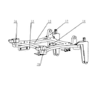
Fig. 4 is the structural representation of silicon chip silk-screen platform assembly support 30 of the present invention
Fig. 5 is the structural representation of silk-screen of the present invention mechanism driven unit 29.
Specific embodiment
Photovoltaic silicon chip automatic screen printer structure, comprise PLC and silicon chip silk-screen platform assembly 32, silicon chip silk-screen platform assembly 32 is arranged on above the silicon chip silk-screen platform assembly support 30, silicon chip silk-screen platform assembly support 30 is movably arranged on above the silk-screen mechanism driven unit 29 by translation back-up block 16, between silicon chip silk-screen platform assembly 32 and silicon chip silk-screen platform assembly support 30, be provided with vision location and silicon chip silk-screen workbench 31, in the medium pore of the table top 1 of silk-screen mechanism driven unit 29, be provided with the screw 2 of the precision ball screw mechanism that vertical direction up and down is provided with, the screw 2 of precision ball screw mechanism by synchronously with 4 with table top 1 bottom surface that is fixedly installed on silk-screen mechanism driven unit 29 on the output shaft of servomotor 5 on the synchronous pulley that is provided be connected, PLC control servomotor 5 rises or falls thereby drive leading screw 3 by with 4 the screw 2 of precision ball screw mechanism being rotated in the medium pore of the table top 1 of silk-screen mechanism driven unit 29 synchronously.The base plate of the top of the leading screw 3 of precision ball screw mechanism and vision location and silicon chip silk-screen workbench 31 links together, thereby also just realizes the lifting of vision location and silicon chip silk-screen workbench 31.On the table top 1 of silk-screen mechanism driven unit 29, be set with four leads 27 by bolt 11, the base plate of the splined shaft 28 in the lead 27 and vision location and silicon chip silk-screen workbench 31 is connected, and the precision when finishing vision location and 31 liftings of silicon chip silk-screen workbench leads.Vision location and silicon chip silk-screen workbench 31 are provided with four vision position observation windows 26, below each vision position observation window 26, be provided with vision positioning element 25, the connection lead of vision positioning element 25 is electrically connected with PLC by the circular hole 12 on the table top 1 that is arranged on silk-screen mechanism driven unit 29, vision positioning element 25 feeds back to PLC with the situation of silicon chip, and PLC adjusts silicon chip silk-screen platform assembly 32 according to these information.After passing from the centre bore 13 of silicon chip silk-screen platform assembly support 30, vision location and silicon chip silk-screen workbench 31 be arranged on below the silk screen of silicon chip silk-screen platform assembly 32; On the left and right horizontal direction of the table top 1 of silk-screen mechanism driven unit 29, be respectively arranged with an X to linear electric motors 6 and the 2nd X to linear electric motors 7, the one X is connected to guide plate to the X of output shaft 8 below being fixedly installed on silicon chip silk-screen platform assembly support 30 of linear electric motors 6, the 2nd X is connected to guide plate 14 to the 2nd X of output shaft below being fixedly installed on silicon chip silk-screen platform assembly support 30 of linear electric motors 7, the front and back horizontal direction of the table top 1 of silk-screen mechanism driven unit 29 is provided with Y to linear electric motors 9, and Y is connected to guide plate 15 to the Y of output shaft 10 below being fixedly installed on silicon chip silk-screen platform assembly support 30 of linear electric motors 9.PC is by an X is controlled realization to the position adjustment horizontal plane of silicon chip silk-screen platform assembly 32 on to linear electric motors 7 and Y to linear electric motors 9 to linear electric motors 6 and the 2nd X.
Described silicon chip silk-screen platform assembly support 30 is provided with hinge Connection Block 17, hinge Connection Block 17 is hinged with the hinge 20 that is arranged on silicon chip silk-screen platform assembly 32 base plates one side, be provided with suction iron block 19 at silicon chip silk-screen platform assembly 32 base plate opposite sides, inhale iron block 19 and flexibly connect with the electromagnet 18 that is fixedly installed on the silicon chip silk-screen platform assembly support 30, electromagnet 18 is electrically connected with PLC.PLC can control the energising and the outage of electromagnet 18, thereby realizes electromagnet 18 and the adhesive of inhaling iron block 19 and separate, make silicon chip silk-screen platform assembly 32 relatively silicon chip silk-screen platform assembly support 30 open.
Below the screen printing frame 21 of described silicon chip silk-screen platform assembly 32, be provided with silk screen 22, on screen printing frame 21, be provided with guide rail 23, be movably set with on guide rail 23 and scrape slurry and silk-screen parts 24, PLC drives slurry and 24 work of silk-screen parts of scraping automatically.
The present invention is machinery, electrical equipment and pneumatic composite design, vision system location, many motor-driven, software control mode.During work, when silicon chip is transported to vision location and silicon chip silk-screen workbench 31, PLC control servomotor 5 drives the vision location by leading screw 3 and silicon chip silk-screen workbench 31 arrival silicon slice placed seated position are carried out the negative-pressure adsorption location to silicon chip, being positioned at four cameras on the vision positioning element and light source simultaneously begins to start for silicon chip and takes pictures, with four of silicon chip how much edges and be positioned at four benchmark on the web plate of its top and indicate point and take simultaneously, above data can be transferred in the data exchange card of two interior triple IEEE 1394b communication channels of screen printer PLC before the silk-screen.Four benchmark according to four of the silicon chip that obtains how much edges and web plate indicate the relative positions of putting, the silk-screen software systems make the position of web plate align silicon chip by the accurate adjustment that calculating and process printing mechanism drive adjustment component, be that three X-Y-θ coordinates in printing mechanism's adjustment component are adjusted the motor projecting shafts and begun respectively to stretch, the live bearing that connects on it can promote two X on printing mechanism's adjustment component to guide rail and Y translation in guide rail is done X-Y plane, promptly form the adjustment of X-Y-θ coordinate, because four translation cushion blocks that printing mechanism supports below the member of translational lay respectively on four fulcrum ball bearings of printing mechanism's driving adjustment component, form the plane mechanism of 4 contacts, therefore, silicon chip silk-screen platform assembly support 30 can drive silicon chip silk-screen platform assembly 32 on it and make Three Degree Of Freedom X-Y-θ adjustment in the level and smooth plane freely.After adjustment finishes, leading screw 3 drives the vision location and silicon chip silk-screen workbench 31 continues the silk-screen position that rising arrives screen printing parts below, silicon chip silk-screen platform assembly 32 scrape the slurry and silk-screen parts 24 according to typography by the adjustment of scraper pressure control valve, the scraper lifting position is adjusted out by the stopper slot and the stop screw of two groups low friction cylinders on it simultaneously, the web plate of below is installed on the screen printing frame 21 in the screen printing parts and by four groups of clamping cylinders it is compressed, and scraper is carrying out silk-screen according to required silk-screen speed to the silicon chip on the silk-screen platform assembly by two closed slides guiding under the drive of motor synchronous band.
Claims (3)
1. photovoltaic silicon chip automatic screen printer structure, comprise PLC and silicon chip silk-screen platform assembly (32), silicon chip silk-screen platform assembly (32) is arranged on above the silicon chip silk-screen platform assembly support (30), silicon chip silk-screen platform assembly support (30) is movably arranged on above the silk-screen mechanism driven unit (29) by translation back-up block (16), between silicon chip silk-screen platform assembly (32) and silicon chip silk-screen platform assembly support (30), be provided with vision location and silicon chip silk-screen workbench (31), it is characterized in that, in the medium pore of the table top (1) of silk-screen mechanism driven unit (29), be provided with the screw (2) of the precision ball screw mechanism that vertical direction up and down is provided with, the synchronous pulley that is provided with on the output shaft of the screw of precision ball screw mechanism (2) by the servomotor (5) on synchronous band (4) and table top (1) bottom surface that is fixedly installed on silk-screen mechanism driven unit (29) is connected, the base plate of the top of the leading screw of precision ball screw mechanism (3) and vision location and silicon chip silk-screen workbench (31) links together, PLC control servomotor (5) is realized leading screw (3) and is arranged on the vision location on leading screw (3) top and the lifting of silicon chip silk-screen workbench (31) by being with (4) synchronously, table top (1) at silk-screen mechanism driven unit (29) upward is set with four leads (27) by bolt (11), splined shaft (28) in the lead (27) is connected with the base plate of vision location and silicon chip silk-screen workbench (31) to finish the precision guiding to vision location and silicon chip silk-screen workbench (31) lifting, vision location and silicon chip silk-screen workbench (31) are provided with four vision position observation windows (26), below each vision position observation window (26), be provided with vision positioning element (25), the connection lead of vision positioning element (25) is electrically connected with PLC by the circular hole (12) on the table top (1) that is arranged on silk-screen mechanism driven unit (29), is arranged on after vision location and silicon chip silk-screen workbench (31) pass from the centre bore (13) of silicon chip silk-screen platform assembly support (30) below the silk screen of silicon chip silk-screen platform assembly (32); On the left and right horizontal direction of the table top (1) of silk-screen mechanism driven unit (29), be respectively arranged with an X to linear electric motors (6) and the 2nd X to linear electric motors (7), the one X is connected to guide plate to the X of output shaft (8) below being fixedly installed on silicon chip silk-screen platform assembly support (30) of linear electric motors (6), the 2nd X is connected to guide plate (14) to the 2nd X of output shaft below being fixedly installed on silicon chip silk-screen platform assembly support (30) of linear electric motors (7), the front and back horizontal direction of the table top (1) of silk-screen mechanism driven unit (29) is provided with Y to linear electric motors (9), and Y is connected to guide plate (15) to the Y of output shaft (10) below being fixedly installed on silicon chip silk-screen platform assembly support (30) of linear electric motors (9).
2. a kind of photovoltaic silicon chip automatic screen printer structure according to claim 1, it is characterized in that, described silicon chip silk-screen platform assembly support (30) is provided with hinge Connection Block (17), hinge Connection Block (17) is hinged with the hinge (20) that is arranged on silicon chip silk-screen platform assembly (32) base plate one side, be provided with suction iron block (19) at silicon chip silk-screen platform assembly (32) base plate opposite side, inhale iron block (19) and flexibly connect with the electromagnet (18) that is fixedly installed on the silicon chip silk-screen platform assembly support (30), electromagnet (18) is electrically connected with PLC.
3. a kind of photovoltaic silicon chip automatic screen printer structure according to claim 1, it is characterized in that, below the screen printing frame (21) of described silicon chip silk-screen platform assembly (32), be provided with silk screen (22), on screen printing frame (21), be provided with guide rail (23), on guide rail (23), be movably set with and scrape slurry and silk-screen parts (24).
Priority Applications (1)
| Application Number | Priority Date | Filing Date | Title |
|---|---|---|---|
| CN2011102161042A CN102294879B (en) | 2011-07-30 | 2011-07-30 | Automatic silk screening mechanism of photovoltaic silicon wafers |
Applications Claiming Priority (1)
| Application Number | Priority Date | Filing Date | Title |
|---|---|---|---|
| CN2011102161042A CN102294879B (en) | 2011-07-30 | 2011-07-30 | Automatic silk screening mechanism of photovoltaic silicon wafers |
Publications (2)
| Publication Number | Publication Date |
|---|---|
| CN102294879A true CN102294879A (en) | 2011-12-28 |
| CN102294879B CN102294879B (en) | 2013-04-17 |
Family
ID=45355660
Family Applications (1)
| Application Number | Title | Priority Date | Filing Date |
|---|---|---|---|
| CN2011102161042A Active CN102294879B (en) | 2011-07-30 | 2011-07-30 | Automatic silk screening mechanism of photovoltaic silicon wafers |
Country Status (1)
| Country | Link |
|---|---|
| CN (1) | CN102294879B (en) |
Cited By (12)
| Publication number | Priority date | Publication date | Assignee | Title |
|---|---|---|---|---|
| CN102658716A (en) * | 2012-05-30 | 2012-09-12 | 东莞市科隆威自动化设备有限公司 | Novel vision alignment system |
| CN102673106A (en) * | 2012-05-09 | 2012-09-19 | 华中科技大学 | Silk screen print positioning equipment and method for photovoltaic solar silicon chip |
| CN105034559A (en) * | 2015-09-15 | 2015-11-11 | 深圳市和田古德自动化设备有限公司 | Correction device for printing technology of PCB plate with length of 600mm or more |
| CN105690982A (en) * | 2015-12-31 | 2016-06-22 | 东旭科技集团有限公司 | MPDP electrode printing system for glass assembly |
| CN105774198A (en) * | 2016-05-06 | 2016-07-20 | 东莞市科隆威自动化设备有限公司 | Steel screen adjusting method of photovoltaic solar screen printer and mechanism thereof |
| CN105799314A (en) * | 2016-05-06 | 2016-07-27 | 东莞市科隆威自动化设备有限公司 | Multifunctional printing machine |
| CN105835521A (en) * | 2016-05-06 | 2016-08-10 | 东莞市科隆威自动化设备有限公司 | Drilling printing machine |
| CN106965540A (en) * | 2017-04-28 | 2017-07-21 | 东莞市安达自动化设备有限公司 | A kind of multi-shaft interlocked adjusting apparatus |
| CN108674012A (en) * | 2018-06-21 | 2018-10-19 | 珠海镇东有限公司 | Screen printer stepper drive automatic aligning platform |
| CN109501443A (en) * | 2018-12-07 | 2019-03-22 | 江西普维智能科技有限公司 | A kind of automatic aligning high speed rotating plate screen printing device |
| CN110077098A (en) * | 2019-06-17 | 2019-08-02 | 四川航天职业技术学院 | Solder(ing) paste silk-screen plateform system |
| CN112060751A (en) * | 2020-09-15 | 2020-12-11 | 东莞光韵达光电科技有限公司 | Nano-coating laser template and plate splicing method thereof |
Citations (4)
| Publication number | Priority date | Publication date | Assignee | Title |
|---|---|---|---|---|
| JPH04331151A (en) * | 1991-01-14 | 1992-11-19 | Sony Corp | Screen automatic exchanging printer |
| CN201437294U (en) * | 2009-06-09 | 2010-04-14 | 深圳德森精密设备有限公司 | Full-automatic vision printing machine and lifting platform system thereof |
| CN201824623U (en) * | 2010-09-08 | 2011-05-11 | 东莞市凯格精密机械有限公司 | Guide rail lifting plate-thickness adjusting mechanism and full-automatic visual printing machine |
| CN202186103U (en) * | 2011-07-30 | 2012-04-11 | 太原风华信息装备股份有限公司 | Photovoltaic silicon wafer automatic silk-screen printing mechanism |
Family Cites Families (1)
| Publication number | Priority date | Publication date | Assignee | Title |
|---|---|---|---|---|
| JP4331151B2 (en) * | 2005-09-20 | 2009-09-16 | 日立建機株式会社 | Working fluid cooling control system for construction machinery |
-
2011
- 2011-07-30 CN CN2011102161042A patent/CN102294879B/en active Active
Patent Citations (4)
| Publication number | Priority date | Publication date | Assignee | Title |
|---|---|---|---|---|
| JPH04331151A (en) * | 1991-01-14 | 1992-11-19 | Sony Corp | Screen automatic exchanging printer |
| CN201437294U (en) * | 2009-06-09 | 2010-04-14 | 深圳德森精密设备有限公司 | Full-automatic vision printing machine and lifting platform system thereof |
| CN201824623U (en) * | 2010-09-08 | 2011-05-11 | 东莞市凯格精密机械有限公司 | Guide rail lifting plate-thickness adjusting mechanism and full-automatic visual printing machine |
| CN202186103U (en) * | 2011-07-30 | 2012-04-11 | 太原风华信息装备股份有限公司 | Photovoltaic silicon wafer automatic silk-screen printing mechanism |
Cited By (17)
| Publication number | Priority date | Publication date | Assignee | Title |
|---|---|---|---|---|
| CN102673106A (en) * | 2012-05-09 | 2012-09-19 | 华中科技大学 | Silk screen print positioning equipment and method for photovoltaic solar silicon chip |
| CN102673106B (en) * | 2012-05-09 | 2014-05-07 | 华中科技大学 | Silk screen print positioning equipment and method for photovoltaic solar silicon chip |
| CN102658716A (en) * | 2012-05-30 | 2012-09-12 | 东莞市科隆威自动化设备有限公司 | Novel vision alignment system |
| CN102658716B (en) * | 2012-05-30 | 2015-04-15 | 东莞市科隆威自动化设备有限公司 | Novel vision alignment system |
| CN105034559A (en) * | 2015-09-15 | 2015-11-11 | 深圳市和田古德自动化设备有限公司 | Correction device for printing technology of PCB plate with length of 600mm or more |
| CN105690982A (en) * | 2015-12-31 | 2016-06-22 | 东旭科技集团有限公司 | MPDP electrode printing system for glass assembly |
| CN105835521A (en) * | 2016-05-06 | 2016-08-10 | 东莞市科隆威自动化设备有限公司 | Drilling printing machine |
| CN105799314A (en) * | 2016-05-06 | 2016-07-27 | 东莞市科隆威自动化设备有限公司 | Multifunctional printing machine |
| CN105774198A (en) * | 2016-05-06 | 2016-07-20 | 东莞市科隆威自动化设备有限公司 | Steel screen adjusting method of photovoltaic solar screen printer and mechanism thereof |
| CN105774198B (en) * | 2016-05-06 | 2018-07-27 | 东莞市科隆威自动化设备有限公司 | A kind of the steel mesh method of adjustment and its mechanism of photovoltaic solar screen process press |
| CN106965540A (en) * | 2017-04-28 | 2017-07-21 | 东莞市安达自动化设备有限公司 | A kind of multi-shaft interlocked adjusting apparatus |
| CN106965540B (en) * | 2017-04-28 | 2023-10-03 | 广东安达智能装备股份有限公司 | Multi-axis linkage adjusting device |
| CN108674012A (en) * | 2018-06-21 | 2018-10-19 | 珠海镇东有限公司 | Screen printer stepper drive automatic aligning platform |
| CN109501443A (en) * | 2018-12-07 | 2019-03-22 | 江西普维智能科技有限公司 | A kind of automatic aligning high speed rotating plate screen printing device |
| CN110077098A (en) * | 2019-06-17 | 2019-08-02 | 四川航天职业技术学院 | Solder(ing) paste silk-screen plateform system |
| CN112060751A (en) * | 2020-09-15 | 2020-12-11 | 东莞光韵达光电科技有限公司 | Nano-coating laser template and plate splicing method thereof |
| CN112060751B (en) * | 2020-09-15 | 2021-10-26 | 东莞光韵达光电科技有限公司 | Nano-coating laser template and plate splicing method thereof |
Also Published As
| Publication number | Publication date |
|---|---|
| CN102294879B (en) | 2013-04-17 |
Similar Documents
| Publication | Publication Date | Title |
|---|---|---|
| CN102294879B (en) | Automatic silk screening mechanism of photovoltaic silicon wafers | |
| CN104191886B (en) | The two-sided engraving machine of a kind of wooden door leaf | |
| CN103496008B (en) | A kind of novel stamp lathe of FPC of automatic loading/unloading | |
| CN101293419B (en) | Digital full-automatic register system for glass screen painting | |
| CN103569641B (en) | Multifunction turning apparatus and method for turning | |
| CN104875514B (en) | Screen printer and screen printing method thereof | |
| CN101676102B (en) | Automatic aligning device | |
| CN205438075U (en) | Automatic board device that grinds of floating PCB board | |
| CN112644149A (en) | Battery piece printing device and printing method | |
| CN105479151A (en) | Automatic screen attaching machine | |
| CN202186103U (en) | Photovoltaic silicon wafer automatic silk-screen printing mechanism | |
| CN205058144U (en) | Automatic cutting device of PCB base plate | |
| CN104842634A (en) | Full-automatic solder paste printing machine | |
| CN204903717U (en) | Keyboard electrical property and sensitive test machine of mistake | |
| CN102756539B (en) | Pattern contraposition method based on double printing stations and device thereof | |
| CN203901916U (en) | Platform correction system of full-automatic solder paste printer | |
| CN204586087U (en) | A kind of high-precision full-automatic screen process press | |
| CN201227883Y (en) | Digital full-automatic register system of glass screen printing | |
| CN104582305A (en) | Glass circuit board based FPC (flexible printed circuit) board hot-pressing device, processing system and method | |
| CN205364798U (en) | Biplate glass screen printing's fine positioning printing platform | |
| CN204820617U (en) | Automatic silk screen printing production line of shoes material | |
| CN210426544U (en) | CCD vision counterpoint mechanism | |
| JP5895130B2 (en) | Screen printing machine and screen printing method | |
| CN204466067U (en) | Based on flexible circuit board hot-press arrangement and the system of processing of glass circuit board | |
| CN104723659A (en) | High-precision full-automatic screen printer and printing method |
Legal Events
| Date | Code | Title | Description |
|---|---|---|---|
| C06 | Publication | ||
| PB01 | Publication | ||
| C10 | Entry into substantive examination | ||
| SE01 | Entry into force of request for substantive examination | ||
| C14 | Grant of patent or utility model | ||
| GR01 | Patent grant | ||
| CP03 | Change of name, title or address |
Address after: 030024 Taiyuan, Shanxi Province, Berlin District, Heping Road, No. 115 Patentee after: CETC Fenghua information equipment Limited by Share Ltd Address before: 030024 Taiyuan Heping Road, Shanxi, No. 115 Patentee before: Taiyuan Fenghua Information Equipment Co., Ltd. |
|
| CP03 | Change of name, title or address |