CN102035552B - Parallel eight-channel high-speed analog signal acquisition device - Google Patents
Parallel eight-channel high-speed analog signal acquisition device Download PDFInfo
- Publication number
- CN102035552B CN102035552B CN 201010544692 CN201010544692A CN102035552B CN 102035552 B CN102035552 B CN 102035552B CN 201010544692 CN201010544692 CN 201010544692 CN 201010544692 A CN201010544692 A CN 201010544692A CN 102035552 B CN102035552 B CN 102035552B
- Authority
- CN
- China
- Prior art keywords
- pin
- fifo buffer
- modular converter
- analog signal
- buffer memory
- Prior art date
- Legal status (The legal status is an assumption and is not a legal conclusion. Google has not performed a legal analysis and makes no representation as to the accuracy of the status listed.)
- Expired - Fee Related
Links
- 238000006243 chemical reaction Methods 0.000 claims abstract description 117
- 239000000872 buffer Substances 0.000 claims abstract description 111
- 230000009466 transformation Effects 0.000 claims description 9
- 108010089790 Eukaryotic Initiation Factor-3 Proteins 0.000 claims description 4
- 102100033132 Eukaryotic translation initiation factor 3 subunit E Human genes 0.000 claims description 4
- 102100028043 Fibroblast growth factor 3 Human genes 0.000 claims description 4
- 102100024061 Integrator complex subunit 1 Human genes 0.000 claims description 4
- 101710092857 Integrator complex subunit 1 Proteins 0.000 claims description 4
- 108050002021 Integrator complex subunit 2 Proteins 0.000 claims description 4
- 101710092886 Integrator complex subunit 3 Proteins 0.000 claims description 4
- 101710092887 Integrator complex subunit 4 Proteins 0.000 claims description 4
- 102100039131 Integrator complex subunit 5 Human genes 0.000 claims description 4
- 101710092888 Integrator complex subunit 5 Proteins 0.000 claims description 4
- 102100030147 Integrator complex subunit 7 Human genes 0.000 claims description 4
- 101710092890 Integrator complex subunit 7 Proteins 0.000 claims description 4
- 102100025254 Neurogenic locus notch homolog protein 4 Human genes 0.000 claims description 4
- 102100037075 Proto-oncogene Wnt-3 Human genes 0.000 claims description 4
- 101100190527 Arabidopsis thaliana PIN5 gene Proteins 0.000 claims description 2
- 101100190528 Arabidopsis thaliana PIN6 gene Proteins 0.000 claims description 2
- 101100190529 Arabidopsis thaliana PIN7 gene Proteins 0.000 claims description 2
- 101100190530 Arabidopsis thaliana PIN8 gene Proteins 0.000 claims description 2
- 108010059419 NIMA-Interacting Peptidylprolyl Isomerase Proteins 0.000 claims description 2
- 101150087393 PIN3 gene Proteins 0.000 claims description 2
- 108010037490 Peptidyl-Prolyl Cis-Trans Isomerase NIMA-Interacting 4 Proteins 0.000 claims description 2
- 102100026114 Peptidyl-prolyl cis-trans isomerase NIMA-interacting 1 Human genes 0.000 claims description 2
- 102100031653 Peptidyl-prolyl cis-trans isomerase NIMA-interacting 4 Human genes 0.000 claims description 2
- 102000007315 Telomeric Repeat Binding Protein 1 Human genes 0.000 claims description 2
- 108010033711 Telomeric Repeat Binding Protein 1 Proteins 0.000 claims description 2
- 230000015654 memory Effects 0.000 claims 43
- 238000004891 communication Methods 0.000 abstract description 4
- 238000007781 pre-processing Methods 0.000 abstract description 3
- 238000000034 method Methods 0.000 description 9
- 238000010586 diagram Methods 0.000 description 3
- 230000005540 biological transmission Effects 0.000 description 2
- 230000009977 dual effect Effects 0.000 description 2
- 238000005516 engineering process Methods 0.000 description 2
- 230000007547 defect Effects 0.000 description 1
- 230000000694 effects Effects 0.000 description 1
- 238000004519 manufacturing process Methods 0.000 description 1
- 230000008054 signal transmission Effects 0.000 description 1
Images

Landscapes
- Design And Manufacture Of Integrated Circuits (AREA)
- Analogue/Digital Conversion (AREA)
Abstract
本发明一种八通道高速模拟信号并行采集装置属于电子通信领域,特别涉及一种带有先进先出缓存多通道高速变化的模拟信号采集,并转换成数字信号传送给外部总线进行处理。信号采集装置采用现场可编程门阵列器件作为八路高速拟信号的预处理单元,带有八个先进先出缓存,配合算术逻辑单元进行八通道高速模拟信号的并行采集。采集装置内置八个先进先出FIFO缓存,其整体结构由FPGA并行采集模块、八个A/D转换模块组成;FPGA并行采集模块由ALU单元、八个三态门和八个FIFO缓存组成。本发明采集速度快,能够保证采集的实时性,解决了八路高速模拟信号的并行采集问题,提高了装置的性能。
The invention relates to an eight-channel high-speed parallel acquisition device for analog signals, which belongs to the field of electronic communication, and particularly relates to an analog signal acquisition with first-in-first-out buffer and multi-channel high-speed change, which is converted into digital signals and transmitted to an external bus for processing. The signal acquisition device adopts the field programmable gate array device as the preprocessing unit of the eight-channel high-speed analog signal, with eight first-in-first-out buffers, and cooperates with the arithmetic logic unit to perform parallel acquisition of the eight-channel high-speed analog signal. The acquisition device has eight first-in-first-out FIFO buffers built in, and its overall structure is composed of FPGA parallel acquisition module and eight A/D conversion modules; FPGA parallel acquisition module is composed of ALU unit, eight tri-state gates and eight FIFO buffers. The invention has fast acquisition speed, can ensure real-time acquisition, solves the problem of parallel acquisition of eight high-speed analog signals, and improves the performance of the device.
Description
技术领域 technical field
本发明一种八通道高速模拟信号并行采集装置属于电子通信领域,特别涉及一种带有先进先出缓存多通道高速变化的模拟信号采集,并转换成数字信号传送给外部总线进行处理的信号采集装置。The invention relates to an eight-channel high-speed analog signal parallel acquisition device, which belongs to the field of electronic communication, and particularly relates to a signal acquisition with a first-in-first-out buffer multi-channel high-speed change, and converts it into a digital signal and transmits it to an external bus for processing. device.
背景技术 Background technique
在通信技术领域,数字信号传输稳定、易于控制和处理,是当前应用最多的通信方式。在实际应用中,很多信号源为模拟信号,例如从传感器感知的信号为连续变化的电压或电流信号,这些信号需要转换成数字信号。对于一般的低速模拟信号,可以通过一个微控制单元控制一个模拟/数字转换器(以下简称A/D)来实现,但是当所采集的模拟信号为多路并且变化特别快时,很难保证所采集的模拟信号不失真。在申请号为200710140206,发明人为蔡仁哲的发明专利“数字模拟转换器及转换方法”中,公告了一种数字模拟转换器,是基于单路的转换方法而提出的,不能对多路模拟信号进行分时高速采集处理。在申请号为201010217051.1的发明专利“双MCU控制多通道高速模拟信号采集器”中,发明人邱铁等提出了一种多通道数字模拟转换器,是基于双MCU协同处理采集信号,不能同时满足八路高速模拟信号的采集要求。In the field of communication technology, digital signal transmission is stable, easy to control and process, and it is currently the most widely used communication method. In practical applications, many signal sources are analog signals, for example, the signals sensed from sensors are continuously changing voltage or current signals, and these signals need to be converted into digital signals. For general low-speed analog signals, it can be realized by controlling an analog/digital converter (hereinafter referred to as A/D) through a micro control unit, but when the collected analog signals are multi-channel and change very fast, it is difficult to guarantee The analog signal is not distorted. In the invention patent "digital-analog converter and conversion method" with the application number 200710140206 and the inventor Cai Renzhe, a digital-analog converter is announced, which is based on a single-channel conversion method and cannot perform multi-channel analog signals. Time-sharing high-speed collection and processing. In the invention patent "dual MCU control multi-channel high-speed analog signal collector" with the application number 201010217051.1, the inventor Qiu Tie and others proposed a multi-channel digital-to-analog converter, which is based on the dual MCU cooperative processing of the acquisition signal, which cannot simultaneously meet the Acquisition requirements of eight high-speed analog signals.
发明内容 Contents of the invention
本发明要解决的技术难题是克服上述现有技术的缺陷,发明一种性能优越的多通道高速模拟信号并行采集装置。如果用传统的信号采集方法,采用单个处理器同时采集八路高速变化的模拟信号,无法保证信号不失真;如果采用多个处理器,会造成资源浪费。而本发明的一种八通道高速模拟信号并行采集装置是采用现场可编程门阵列器件(以下简称FPGA)作为八路高速拟信号的预处理单元,带有八个先进先出缓存,配合算术逻辑单元(以下简称ALU单元)进行八通道高速模拟信号的并行采集。采集速度快,能够保证采集的实时性,解决了八路高速模拟信号的并行采集问题,提高了装置的性能。The technical problem to be solved by the present invention is to overcome the defects of the above-mentioned prior art and to invent a multi-channel high-speed analog signal parallel acquisition device with superior performance. If the traditional signal acquisition method is used, a single processor is used to simultaneously acquire eight high-speed analog signals, which cannot guarantee that the signal will not be distorted; if multiple processors are used, resources will be wasted. And a kind of eight-channel high-speed analog signal parallel acquisition device of the present invention is to adopt field programmable gate array device (hereinafter referred to as FPGA) as the preprocessing unit of eight-way high-speed analog signal, with eight first-in-first-out buffers, cooperates arithmetic logic unit (hereinafter referred to as the ALU unit) for parallel acquisition of eight-channel high-speed analog signals. The collection speed is fast, which can ensure the real-time collection, solve the problem of parallel collection of eight high-speed analog signals, and improve the performance of the device.
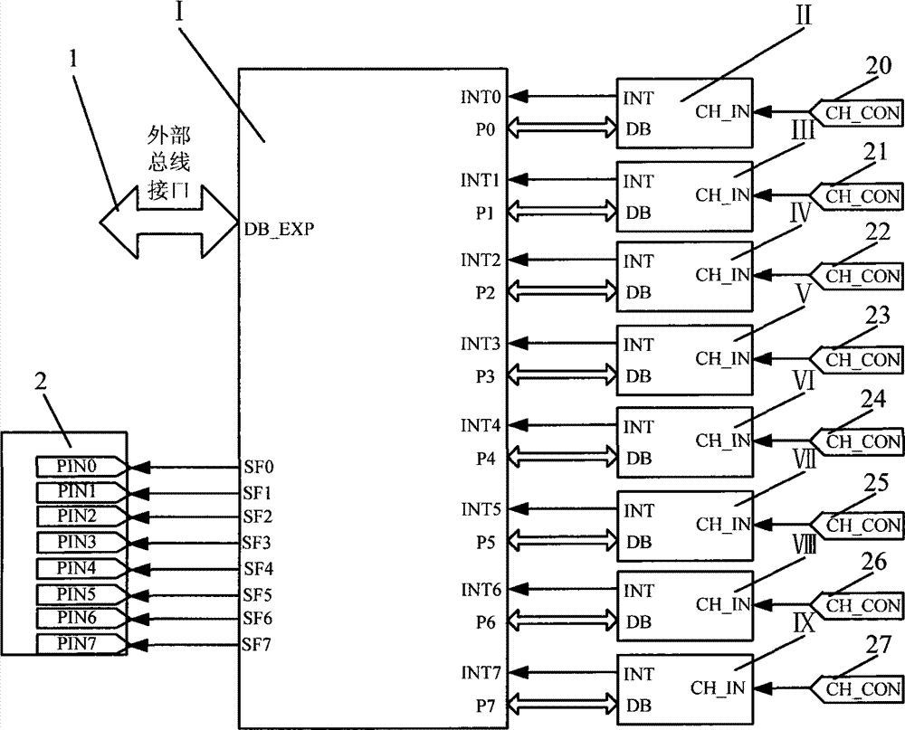
本发明采用的技术方案是一种八通道高速模拟信号并行采集装置,信号采集装置采用现场可编程门阵列器件作为八路高速拟信号的预处理单元,带有八个先进先出缓存,配合算术逻辑单元进行八通道高速模拟信号的并行采集;采集装置内置八个先进先出FIFO缓存,其整体结构由FPGA并行采集模块I、第一A/D转换模块II、第二A/D转换模块III、第三A/D转换模块IV、第四A/D转换模块V、第五A/D转换模块VI、第六A/D转换模块VII、第七A/D转换模块VIII和第八A/D转换模块IX组成。FPGA并行采集模块I由ALU单元3、第一三态门4、第一FIFO缓存5、第二三态门6、第二FIFO缓存7、第三三态门8、第三FIFO缓存9、第四三态门10、第四FIFO缓存11、第五三态门12、第五FIFO缓存13、第六三态门14、第六FIFO缓存15、第七三态门16、第七FIFO缓存17、第八三态门18、第八FIFO缓存19组成,其中每个FIFO缓存占有8个字节大小。The technical solution adopted by the present invention is an eight-channel high-speed analog signal parallel acquisition device. The signal acquisition device adopts a field programmable gate array device as a preprocessing unit for eight high-speed analog signals, and has eight first-in-first-out buffers, which cooperate with arithmetic logic The unit performs parallel acquisition of eight-channel high-speed analog signals; the acquisition device has eight first-in-first-out FIFO buffers built in, and its overall structure consists of FPGA parallel acquisition module I, the first A/D conversion module II, the second A/D conversion module III, The third A/D conversion module IV, the fourth A/D conversion module V, the fifth A/D conversion module VI, the sixth A/D conversion module VII, the seventh A/D conversion module VIII and the eighth A/D Transformation module IX composition. FPGA parallel collection module 1 is by ALU unit 3, the first tri-state gate 4, the first FIFO cache 5, the second tri-state gate 6, the second FIFO cache 7, the third tri-state gate 8, the third FIFO cache 9, the second tri-state gate Four tri-state gates 10, fourth FIFO buffer 11, fifth tri-state gate 12, fifth FIFO buffer 13, sixth tri-state gate 14, sixth FIFO buffer 15, seventh tri-state gate 16, seventh FIFO buffer 17 , an eighth tri-state gate 18, and an eighth FIFO buffer 19, wherein each FIFO buffer occupies 8 bytes in size.
FPGA并行采集模块I的中断第0引脚INT0与第一A/D转换模块II的A/D转换中断引脚INT相连,用于接收第一A/D转换模块II的转换完毕中断请求;FPGA并行采集模块I的通用输入输出第0端口P0与第一A/D转换模块II的A/D转换数据总线DB相连,用于接收第一A/D转换模块II的转换结果数据;第一A/D转换模块II的模拟信号输入通道CH_IN与第一模拟信号输入端20的模拟信号输入端接线引脚CH_CON相连,作为第一路模拟号的输入端;FPGA并行采集模块I的第一FIFO缓存状态引脚SF0与状态总线接线端子2的状态总线接线端子第0引脚PIN0相连,用于查询第一FIFO缓存5的状态信息。The interrupt 0th pin INT0 of the FPGA parallel acquisition module I is connected with the A/D conversion interrupt pin INT of the first A/D conversion module II, and is used to receive the conversion completion interrupt request of the first A/D conversion module II; FPGA The general input and output 0th port P0 of the parallel acquisition module I is connected with the A/D conversion data bus DB of the first A/D conversion module II, and is used to receive the conversion result data of the first A/D conversion module II; the first A The analog signal input channel CH_IN of the /D conversion module II is connected with the analog signal input connection pin CH_CON of the first analog
FPGA并行采集模块I的中断第1引脚INT1与第二A/D转换模块III的A/D转换中断引脚INT相连,用于接收第二A/D转换模块III的转换完毕中断请求;FPGA并行采集模块I的通用输入输出第1端口P1与第二A/D转换模块III的A/D转换数据总线DB相连,用于接收第二A/D转换模块III的转换结果数据;第二A/D转换模块III的模拟信号输入通道CH_IN与第二模拟信号输入端21的模拟信号输入端接线引脚CH_CON相连,作为第二路模拟号的输入端。FPGA并行采集模块I的第二FIFO缓存状态引脚SF1与状态总线接线端子2的状态总线接线端子第1引脚PIN1相连,用于查询第二FIFO缓存7的状态信息。The interrupt first pin INT1 of FPGA parallel acquisition module I is connected with the A/D conversion interrupt pin INT of the second A/D conversion module III, and is used to receive the conversion completion interrupt request of the second A/D conversion module III; FPGA The general input and output first port P1 of the parallel acquisition module I is connected with the A/D conversion data bus DB of the second A/D conversion module III, and is used to receive the conversion result data of the second A/D conversion module III; the second A The analog signal input channel CH_IN of the /D conversion module III is connected to the analog signal input terminal connection pin CH_CON of the second analog
FPGA并行采集模块I的中断第2引脚INT2与第三A/D转换模块IV的A/D转换中断引脚INT相连,用于接收第三A/D转换模块IV的转换完毕中断请求;FPGA并行采集模块I的通用输入输出第2端口P2与第三A/D转换模块IV的A/D转换数据总线DB相连,用于接收第三A/D转换模块IV的转换结果数据;第三A/D转换模块IV的模拟信号输入通道CH_IN与第三模拟信号输入端22的模拟信号输入端接线引脚CH_CON相连,作为第三路模拟号的输入端。FPGA并行采集模块I的第三FIFO缓存状态引脚SF2与状态总线接线端子2的状态总线接线端子第2引脚PIN2相连,用于查询第三FIFO缓存9的状态信息。The interrupt 2nd pin INT2 of FPGA parallel acquisition module 1 is connected with the A/D conversion interrupt pin INT of the 3rd A/D conversion module IV, is used to receive the conversion completion interrupt request of the 3rd A/D conversion module IV; FPGA The general input and output the 2nd port P2 of parallel acquisition module 1 is connected with the A/D conversion data bus DB DB of the 3rd A/D conversion module IV, is used to receive the conversion result data of the 3rd A/D conversion module IV; The analog signal input channel CH_IN of the /D conversion module IV is connected to the analog signal input terminal connection pin CH_CON of the third analog
FPGA并行采集模块I的中断第3引脚INT3与第四A/D转换模块V的A/D转换中断引脚INT相连,用于接收第四A/D转换模块V的转换完毕中断请求;FPGA并行采集模块I的通用输入输出第3端口P3与第四A/D转换模块V的A/D转换数据总线DB相连,用于接收第四A/D转换模块V的转换结果数据;第四A/D转换模块V的模拟信号输入通道CH_IN与第四模拟信号输入端23的模拟信号输入端接线引脚CH_CON相连,作为第四路模拟号的输入端。FPGA并行采集模块I的第四FIFO缓存状态引脚SF3与状态总线接线端子2的状态总线接线端子第3引脚PIN3相连,用于查询第四FIFO缓存11的状态信息。The interrupt 3rd pin INT3 of FPGA parallel acquisition module 1 is connected with the A/D conversion interrupt pin INT of the 4th A/D conversion module V, is used to receive the conversion completion interrupt request of the 4th A/D conversion module V; FPGA The 3rd general input and output port P3 of parallel acquisition module 1 is connected with the A/D conversion data bus DB of the 4th A/D conversion module V, is used to receive the conversion result data of the 4th A/D conversion module V; The analog signal input channel CH_IN of the /D conversion module V is connected to the analog signal input terminal connection pin CH_CON of the fourth analog
FPGA并行采集模块I的中断第4引脚INT4与第五A/D转换模块VI的A/D转换中断引脚INT相连,用于接收第五A/D转换模块VI的转换完毕中断请求;FPGA并行采集模块I的通用输入输出第4端口P4与第五A/D转换模块VI的A/D转换数据总线DB相连,用于接收第五A/D转换模块VI的转换结果数据;第五A/D转换模块VI的模拟信号输入通道CH_IN与第五模拟信号输入端24的模拟信号输入端接线引脚CH_CON相连,作为第五路模拟号的输入端。FPGA并行采集模块I的第五FIFO缓存状态引脚SF4与状态总线接线端子2的状态总线接线端子第4引脚PIN4相连,用于查询第五FIFO缓存13的状态信息。The interrupt 4th pin INT4 of FPGA parallel acquisition module 1 is connected with the A/D conversion interrupt pin INT of the 5th A/D conversion module VI, is used to receive the conversion completion interrupt request of the 5th A/D conversion module VI; FPGA The general input and output 4th port P4 of parallel acquisition module 1 is connected with the A/D conversion data bus DB of the 5th A/D conversion module VI, is used to receive the conversion result data of the 5th A/D conversion module VI; The 5th A The analog signal input channel CH_IN of the /D conversion module VI is connected to the analog signal input terminal connection pin CH_CON of the fifth analog
FPGA并行采集模块I的中断第5引脚INT5与第六A/D转换模块VII的A/D转换中断引脚INT相连,用于接收第六A/D转换模块VII的转换完毕中断请求;FPGA并行采集模块I的通用输入输出第5端口P5与第六A/D转换模块VII的A/D转换数据总线DB相连,用于接收第六A/D转换模块VII的转换结果数据;第六A/D转换模块VII的模拟信号输入通道CH_IN与第六模拟信号输入端25的模拟信号输入端接线引脚CH_CON相连,作为第六路模拟号的输入端。FPGA并行采集模块I的第六FIFO缓存状态引脚SF5与状态总线接线端子2的状态总线接线端子第5引脚PIN5相连,用于查询第六FIFO缓存15的状态信息。The interrupt 5th pin INT5 of FPGA parallel acquisition module 1 is connected with the A/D conversion interrupt pin INT of the 6th A/D conversion module VII, is used to receive the conversion completion interrupt request of the 6th A/D conversion module VII; FPGA The 5th port P5 of the universal input and output of the parallel acquisition module 1 is connected with the A/D conversion data bus DB of the sixth A/D conversion module VII, and is used to receive the conversion result data of the sixth A/D conversion module VII; the sixth A The analog signal input channel CH_IN of the /D conversion module VII is connected to the analog signal input terminal connection pin CH_CON of the sixth analog
FPGA并行采集模块I的中断第6引脚INT6与第七A/D转换模块VIII的A/D转换中断引脚INT相连,用于接收第七A/D转换模块VIII的转换完毕中断请求;FPGA并行采集模块I的通用输入输出第6端口P6与第七A/D转换模块VIII的A/D转换数据总线DB相连,用于接收第七A/D转换模块VIII的转换结果数据;第七A/D转换模块VIII的模拟信号输入通道CH_IN与第七模拟信号输入端26的模拟信号输入端接线引脚CH_CON相连,作为第七路模拟号的输入端。FPGA并行采集模块I的第七FIFO缓存状态引脚SF6与状态总线接线端子2的状态总线接线端子第6引脚PIN6相连,用于查询第七FIFO缓存17的状态信息。The interrupt 6th pin INT6 of FPGA parallel acquisition module 1 is connected with the A/D conversion interrupt pin INT of the seventh A/D conversion module VIII, and is used to receive the conversion completion interrupt request of the seventh A/D conversion module VIII; FPGA The 6th port P6 of the universal input and output of the parallel acquisition module 1 is connected with the A/D conversion data bus DB of the seventh A/D conversion module VIII, and is used to receive the conversion result data of the seventh A/D conversion module VIII; the seventh A The analog signal input channel CH_IN of the /D conversion module VIII is connected to the analog signal input terminal connection pin CH_CON of the seventh analog
FPGA并行采集模块I的中断第7引脚INT7与第八A/D转换模块IX的A/D转换中断引脚INT相连,用于接收第八A/D转换模块IX的转换完毕中断请求;FPGA并行采集模块I的通用输入输出第7端口P7与第八A/D转换模块IX的A/D转换数据总线DB相连,用于接收第八A/D转换模块IX的转换结果数据;第八A/D转换模块IX的模拟信号输入通道CH_IN与第八模拟信号输入端27的模拟信号输入端接线引脚CH_CON相连,作为第八路模拟号的输入端。FPGA并行采集模块I的第八FIFO缓存状态引脚SF7与状态总线接线端子2的状态总线接线端子第7引脚PIN7相连,用于查询第八FIFO缓存19的状态信息。The interrupt 7th pin INT7 of FPGA parallel acquisition module 1 is connected with the A/D conversion interrupt pin INT of the eighth A/D conversion module IX, and is used to receive the conversion completion interrupt request of the eighth A/D conversion module IX; FPGA The 7th port P7 of the universal input and output of the parallel acquisition module 1 is connected with the A/D conversion data bus DB of the eighth A/D conversion module IX, and is used to receive the conversion result data of the eighth A/D conversion module IX; the eighth A The analog signal input channel CH_IN of the /D conversion module IX is connected to the analog signal input terminal connection pin CH_CON of the eighth analog
在FPGA并行采集模块I中,通用输入输出第0端口P0与第一FIFO缓存5相连,第一FIFO缓存5通过第一三态门4连接到内部总线28,第一三态门4由ALU单元3的片选信号第0控制端CS0控制,第一FIFO缓存5是否为空由第一FIFO缓存状态引脚SF0进行标识,中断第0引脚INT0作为ALU单元3的输入信号;In the FPGA parallel acquisition module 1, the 0th port P0 of the general input and output is connected with the first FIFO buffer 5, and the first FIFO buffer 5 is connected to the internal bus 28 by the first tri-state gate 4, and the first tri-state gate 4 is controlled by the ALU unit The chip selection signal of 3 is controlled by the 0th control terminal CS0, whether the first FIFO buffer 5 is empty is identified by the first FIFO buffer status pin SF0, and the 0th pin INT0 is interrupted as the input signal of the ALU unit 3;
通用输入输出第1端口P1与第二FIFO缓存7相连,第二FIFO缓存7通过第二三态门6连接到内部总线28,第二三态门6由ALU单元3的片选信号第1控制端CS1控制,第二FIFO缓存7是否为空由第二FIFO缓存状态引脚SF1进行标识,中断第1引脚INT1作为ALU单元3的输入信号;The first general-purpose input and output port P1 is connected to the second FIFO buffer 7, and the second FIFO buffer 7 is connected to the internal bus 28 through the second tri-state gate 6, and the second tri-state gate 6 is controlled by the first chip selection signal of the ALU unit 3 Terminal CS1 control, whether the second FIFO cache 7 is empty is marked by the second FIFO cache status pin SF1, and interrupts the first pin INT1 as the input signal of the ALU unit 3;
通用输入输出第2端口P2与第三FIFO缓存9相连,第三FIFO缓存9通过第三三态门8连接到内部总线28,第三三态门8由ALU单元3的片选信号第2控制端CS2控制,第三FIFO缓存9是否为空由第三FIFO缓存状态引脚SF2进行标识,中断第2引脚INT2作为ALU单元3的输入信号;The second general-purpose input and output port P2 is connected to the third FIFO buffer 9, and the third FIFO buffer 9 is connected to the internal bus 28 through the third tri-state gate 8, and the third tri-state gate 8 is controlled by the chip select signal 2 of the ALU unit 3 Terminal CS2 control, whether the third FIFO cache 9 is empty is identified by the third FIFO cache status pin SF2, and the second pin INT2 is interrupted as the input signal of the ALU unit 3;
通用输入输出第3端口P3与第四FIFO缓存11相连,第四FIFO缓存11通过第四三态门10连接到内部总线28,第四三态门10由ALU单元3的片选信号第3控制端CS3控制,第四FIFO缓存11是否为空由第四FIFO缓存状态引脚SF3进行标识,中断第3引脚INT3作为ALU单元3的输入信号;The third general-purpose input and output port P3 is connected to the fourth FIFO buffer 11, and the fourth FIFO buffer 11 is connected to the internal bus 28 through the fourth tri-state gate 10, and the fourth tri-state gate 10 is controlled by the chip select signal 3 of the ALU unit 3 Controlled by terminal CS3, whether the fourth FIFO cache 11 is empty is identified by the fourth FIFO cache status pin SF3, and the third pin INT3 is interrupted as the input signal of the ALU unit 3;
通用输入输出第4端口P4与第五FIFO缓存13相连,第五FIFO缓存13通过第五三态门12连接到内部总线28,第五三态门12由ALU单元3的片选信号第4控制端CS4控制,第五FIFO缓存13是否为空由第五FIFO缓存状态引脚SF4进行标识,中断第4引脚INT4作为ALU单元3输入信号;The fourth general-purpose input and output port P4 is connected to the fifth FIFO buffer 13, and the fifth FIFO buffer 13 is connected to the internal bus 28 through the fifth tri-state gate 12, and the fifth tri-state gate 12 is controlled by the chip select signal 4 of the ALU unit 3. Controlled by terminal CS4, whether the fifth FIFO cache 13 is empty is identified by the fifth FIFO cache status pin SF4, and the fourth pin INT4 is interrupted as the ALU unit 3 input signal;
通用输入输出第5端口P5与第六FIFO缓存15相连,第六FIFO缓存15通过第六三态门14连接到内部总线28,第六三态门14由ALU单元3的片选信号第5控制端CS5控制,第六FIFO缓存15是否为空由第六FIFO缓存状态引脚SF5进行标识,中断第5引脚INT5作为ALU单元3的输入信号;The fifth general-purpose input and output port P5 is connected to the sixth FIFO buffer 15, the sixth FIFO buffer 15 is connected to the internal bus 28 through the sixth tri-state gate 14, and the sixth tri-state gate 14 is controlled by the chip selection signal 5 of the ALU unit 3 Controlled by end CS5, whether the sixth FIFO cache 15 is empty is marked by the sixth FIFO cache status pin SF5, and the fifth pin INT5 is interrupted as the input signal of ALU unit 3;
通用输入输出第6端口P6与第七FIFO缓存17相连,第七FIFO缓存17通过第七三态门16连接到内部总线28,第七三态门16由ALU单元3的片选信号第6控制端CS6控制,第七FIFO缓存17是否为空由第七FIFO缓存状态引脚SF6进行标识,中断第6引脚INT6作为ALU单元3的输入信号;The sixth general-purpose input and output port P6 is connected to the seventh FIFO buffer 17, and the seventh FIFO buffer 17 is connected to the internal bus 28 through the seventh tri-state gate 16, and the seventh tri-state gate 16 is controlled by the chip selection signal 6 of the ALU unit 3 End CS6 control, whether the seventh FIFO cache 17 is empty is identified by the seventh FIFO cache status pin SF6, and the 6th pin INT6 is interrupted as the input signal of the ALU unit 3;
通用输入输出第7端口P7与第八FIFO缓存19相连,第八FIFO缓存19通过第八三态门18连接到内部总线28,第八三态门18由ALU单元3的片选信号第7控制端CS7控制,第八FIFO缓存19是否为空由第八FIFO缓存状态引脚SF7进行标识,中断第7引脚INT7作为ALU单元3的输入信号;The seventh general-purpose input and output port P7 is connected to the eighth FIFO buffer 19, and the eighth FIFO buffer 19 is connected to the internal bus 28 through the eighth tri-state gate 18, and the eighth tri-state gate 18 is controlled by the chip selection signal 7 of the ALU unit 3. Terminal CS7 control, whether the eighth FIFO cache 19 is empty is identified by the eighth FIFO cache status pin SF7, and interrupts the seventh pin INT7 as the input signal of the ALU unit 3;
外部总线接口1与的内部总线28的外部总线端口DB_EXP连接,可以进行数据输入与输出。The external bus interface 1 is connected to the external bus port DB_EXP of the internal bus 28 for data input and output.
本发明的效果是采用FPGA设计八通道带有先进先出缓存的高速模拟信号并行采集装置,结构新颖,采集信号响应快,各个通道可以同时进行采集,在时间上无需等待,实时性好;总线接口灵活方便,易与控制和扩展;具有良好的可维护,较好的经济性,制造方便,成本低;相对传统多MCU采集方式,功耗低。The effect of the present invention is to adopt FPGA to design eight-channel high-speed analog signal parallel acquisition device with first-in-first-out buffer, novel structure, quick response of acquisition signal, each channel can be acquired simultaneously, no need to wait in time, good real-time performance; bus The interface is flexible and convenient, easy to control and expand; it has good maintainability, good economy, convenient manufacture, and low cost; compared with the traditional multi-MCU acquisition method, the power consumption is low.
附图说明 Description of drawings
图1为一种八通道高速模拟信号并行采集装置的总体结构图,图2为FPGA并行采集模块内部结构图。Figure 1 is an overall structure diagram of an eight-channel high-speed analog signal parallel acquisition device, and Figure 2 is an internal structure diagram of an FPGA parallel acquisition module.
其中,I-FPGA并行采集模块,II-第一A/D转换模块,III-第二A/D转换模块,IV-第三A/D转换模块,V-第四A/D转换模块,VI-第五A/D转换模块,VII-第六A/D转换模块,VIII-第七A/D转换模块,IX-第八A/D转换模块;1-外部总线接口,2-状态总线接线端子,3-ALU单元,4-第一三态门,5-第一FIFO状态缓存,6-第二三态门,7-第二FIFO缓存,8-第三三态门,9-第三FIFO缓存,10-第四三态门,11-第四FIFO缓存,12-第五三态门,13-第五FIFO缓存,14-第六三态门,15-第六FIFO缓存,16-第七三态门,17-第七FIFO缓存,18-第八三态门,19-第八FIFO缓存,20-第一模拟信号输入端,21-第二模拟信号输入端,22-第三模拟信号输入端,23-第四模拟信号输入端,24-第五模拟信号输入端,25-第六模拟信号输入端,26-第七模拟信号输入端,27-第八模拟信号输入端,28-内部总线;DB EXP-外部总线端口,INT0-中断第0引脚,INT1-中断第1引脚,INT2-中断第2引脚,INT3-中断第3引脚,INT4-中断第4引脚,INT5-中断第5引脚,INT6-中断第6引脚,INT7-中断第7引脚,P0-通用输入输出第0端口,P1-通用输入输出第1端口,P2-通用输入输出第2端口,P3-通用输入输出第3端口,P4-通用输入输出第4端口,P5-通用输入输出第5端口,P6-通用输入输出第6端口,P7-通用输入输出第7端口,INT-A/D转换中断引脚,DB-A/D转换模块数据总线,CH_IN-模拟信号输入通道,CH_CON-模拟信号输入端接线引脚,SF0-第-FIFO缓存状态引脚,SF1-第二FIFO缓存状态引脚,SF2-第三FIFO缓存状态引脚,SF3-第四FIFO缓存状态引脚,SF4-第五FIFO缓存状态引脚,SF5-第六FIFO缓存状态引脚,SF6-第七FIFO缓存状态引脚,SF7-第八FIFO缓存状态引脚,PIN0-状态总线接线端子第0引脚,PIN1-状态总线接线端子第1引脚,PIN2-状态总线接线端子第2引脚,PIN3-状态总线接线端子第3引脚,PIN4-状态总线接线端子第4引脚,PIN5-状态总线接线端子第5引脚,PIN6-状态总线接线端子第6引脚,PIN7-状态总线接线端子第7引脚。CS0-片选信号第0控制端,CS1-片选信号第1控制端,CS2-片选信号第2控制端,CS3-片选信号第3控制端,CS4-片选信号第4控制端,CS5-片选信号第5控制端,CS6-片选信号第6控制端,CS7-片选信号第7控制端。Among them, I-FPGA parallel acquisition module, II-the first A/D conversion module, III-the second A/D conversion module, IV-the third A/D conversion module, V-the fourth A/D conversion module, VI -The fifth A/D conversion module, VII-the sixth A/D conversion module, VIII-the seventh A/D conversion module, IX-the eighth A/D conversion module; 1-external bus interface, 2-status bus connection Terminal, 3-ALU unit, 4-first tri-state gate, 5-first FIFO state buffer, 6-second tri-state gate, 7-second FIFO buffer, 8-third tri-state gate, 9-third FIFO buffer, 10-fourth tri-state gate, 11-fourth FIFO buffer, 12-fifth tri-state gate, 13-fifth FIFO buffer, 14-sixth tri-state gate, 15-sixth FIFO buffer, 16- The seventh tri-state gate, 17-the seventh FIFO buffer, 18-the eighth tri-state gate, 19-the eighth FIFO buffer, 20-the first analog signal input terminal, 21-the second analog signal input terminal, 22-the third Analog signal input terminal, 23-fourth analog signal input terminal, 24-fifth analog signal input terminal, 25-sixth analog signal input terminal, 26-seventh analog signal input terminal, 27-eighth analog signal input terminal, 28-internal bus; DB EXP-external bus port, INT0-interrupt pin 0, INT1-interrupt pin 1, INT2-interrupt pin 2, INT3-interrupt pin 3, INT4-interrupt pin 4 Pin, INT5-interrupt pin 5, INT6-interrupt pin 6, INT7-interrupt pin 7, P0-general input and output port 0, P1-general input and output port 1, P2-general input and output port 2 ports, P3-GPIO 3rd port, P4-GPIO 4th port, P5-GPIO 5th port, P6-GPIO 6th port, P7-GPIO 7th port, INT- A/D conversion interrupt pin, DB-A/D conversion module data bus, CH_IN-analog signal input channel, CH_CON-analog signal input connection pin, SF0-first-FIFO cache status pin, SF1-second FIFO Cache status pin, SF2-third FIFO cache status pin, SF3-fourth FIFO cache status pin, SF4-fifth FIFO cache status pin, SF5-sixth FIFO cache status pin, SF6-seventh FIFO Cache status pin, SF7-8th FIFO cache status pin, PIN0-status bus terminal pin 0, PIN1-status bus terminal pin 1, PIN2-status bus terminal pin 2, PIN3- Status bus terminal pin 3, PIN4-status bus terminal pin 4, PIN5-status bus terminal pin 5, PIN6-status bus terminal pin 6, PIN7-status bus terminal pin 7 pin. CS0-the 0th control terminal of the chip selection signal, CS1-the 1st control terminal of the chip selection signal, CS2-the 2nd control terminal of the chip selection signal, CS3-the 3rd control terminal of the chip selection signal, CS4-the 4th control terminal of the chip selection signal, CS5-the 5th control terminal of the chip selection signal, CS6-the 6th control terminal of the chip selection signal, CS7-the 7th control terminal of the chip selection signal.
具体实施方式 Detailed ways
下面结合说明书附图和技术方案详细说明本发明的具体实施方式:The specific embodiment of the present invention is described in detail below in conjunction with description accompanying drawing and technical scheme:
一种八通道高速模拟信号并行采集装置的总体结构图,电路模块组成和连接关系,如说明书附图1所示,FPGA并行采集模块内部结构如图2所示。本发明可以同时采集八路模拟信号,并且此八路信号都可以独立进行,因此本实施例以第一A/D转换模块II采集过程为例,详细说明本发明的实施方式。An overall structure diagram of an eight-channel high-speed analog signal parallel acquisition device, circuit module composition and connection relationship, as shown in Figure 1 of the specification, and the internal structure of the FPGA parallel acquisition module is shown in Figure 2. The present invention can collect eight channels of analog signals at the same time, and these eight channels of signals can be performed independently, so this embodiment takes the acquisition process of the first A/D conversion module II as an example to describe the implementation of the present invention in detail.
模拟信号从第一模拟信号输入端20的模拟信号输入端接线引脚CH_CON输入,由经由模拟信号输入通道CH_IN进入第一A/D转换模块II。第一A/D转换模块II对模拟信号进行采样转换,转换完毕后存入第一FIFO缓存5,并由A/D转换中断引脚INT申请中断。此时,FPGA并行采集模块I的中断第0引脚INT0收到中断请求后,由ALU单元3进行处理。首先ALU单元3将第一FIFO缓存状态引脚SF0置为1,其真值表如下表所示,指示第一FIFO缓存5的数据进入内部总线28;接下来ALU单元3的片选信号第0控制端CS0控制第一三态门4处于开启状态,使第一A/D转换模块II连接到内部总线28,保证数据进行传输,将数据送到外部总线接口1,从而完成一次数据采集和传输。如果第一A/D转换模块II对模拟信号进行采样转换并存入第一FIFO缓存5后,在第一FIFO缓存5中的数据没有被及时取走,由于第一FIFO缓存5具有8个字节的缓存,可以暂时缓存数据。其余七路模拟信号的采集同第一A/D转换模块II的采集方式。The analog signal is input from the analog signal input terminal connection pin CH_CON of the first analog


本发明一种八通道高速模拟信号并行采集装置,FPGA并行采集模块I带有八个FIFO缓存,并实时监测八通道A/D转换模块的采集状态,能够对八路高速变化的模拟信号进行实时采集,信号采集和存缓存数据延迟时间短,效率高,能够适应高速变化的模拟信号采集和处理。采用FPGA硬件可编程技术设计的FPGA并行采集模块I,功率消耗低,响应快,能够进行高速的处理与通道实时切换,外部总线接口简单,具有很强的扩展性和可移植性。The present invention is an eight-channel high-speed analog signal parallel acquisition device. The FPGA parallel acquisition module 1 has eight FIFO caches, and monitors the acquisition status of the eight-channel A/D conversion module in real time, and can collect in real time the eight-way high-speed analog signal. , The delay time of signal acquisition and cache data is short, the efficiency is high, and it can adapt to high-speed changing analog signal acquisition and processing. The FPGA parallel acquisition module I designed with FPGA hardware programmable technology has low power consumption, fast response, high-speed processing and real-time channel switching, simple external bus interface, strong scalability and portability.
Claims (1)
Priority Applications (1)
| Application Number | Priority Date | Filing Date | Title |
|---|---|---|---|
| CN 201010544692 CN102035552B (en) | 2010-11-11 | 2010-11-11 | Parallel eight-channel high-speed analog signal acquisition device |
Applications Claiming Priority (1)
| Application Number | Priority Date | Filing Date | Title |
|---|---|---|---|
| CN 201010544692 CN102035552B (en) | 2010-11-11 | 2010-11-11 | Parallel eight-channel high-speed analog signal acquisition device |
Publications (2)
| Publication Number | Publication Date |
|---|---|
| CN102035552A CN102035552A (en) | 2011-04-27 |
| CN102035552B true CN102035552B (en) | 2013-04-17 |
Family
ID=43887968
Family Applications (1)
| Application Number | Title | Priority Date | Filing Date |
|---|---|---|---|
| CN 201010544692 Expired - Fee Related CN102035552B (en) | 2010-11-11 | 2010-11-11 | Parallel eight-channel high-speed analog signal acquisition device |
Country Status (1)
| Country | Link |
|---|---|
| CN (1) | CN102035552B (en) |
Families Citing this family (1)
| Publication number | Priority date | Publication date | Assignee | Title |
|---|---|---|---|---|
| CN118138043B (en) * | 2024-03-08 | 2025-02-07 | 广芯微电子(广州)股份有限公司 | ADC sampling data output method, device and chip |
Citations (3)
| Publication number | Priority date | Publication date | Assignee | Title |
|---|---|---|---|---|
| US5230071A (en) * | 1987-08-13 | 1993-07-20 | Digital Equipment Corporation | Method for controlling the variable baud rate of peripheral devices |
| CN1143869A (en) * | 1995-06-06 | 1997-02-26 | 环球星有限合伙人公司 | Two-system protocol conversion transceiver repeater |
| CN101551786A (en) * | 2009-05-05 | 2009-10-07 | 大连理工大学 | Manufacturing method of baud rate self-adaptive serial communication repeater |
-
2010
- 2010-11-11 CN CN 201010544692 patent/CN102035552B/en not_active Expired - Fee Related
Patent Citations (3)
| Publication number | Priority date | Publication date | Assignee | Title |
|---|---|---|---|---|
| US5230071A (en) * | 1987-08-13 | 1993-07-20 | Digital Equipment Corporation | Method for controlling the variable baud rate of peripheral devices |
| CN1143869A (en) * | 1995-06-06 | 1997-02-26 | 环球星有限合伙人公司 | Two-system protocol conversion transceiver repeater |
| CN101551786A (en) * | 2009-05-05 | 2009-10-07 | 大连理工大学 | Manufacturing method of baud rate self-adaptive serial communication repeater |
Non-Patent Citations (1)
| Title |
|---|
| 赵亮,冯林,吴振宇.基于FPGA的小型机器人无线通信系统.《计算机工程》.2010,第36卷(第13期), * |
Also Published As
| Publication number | Publication date |
|---|---|
| CN102035552A (en) | 2011-04-27 |
Similar Documents
| Publication | Publication Date | Title |
|---|---|---|
| CN104020691B (en) | It is applicable to the signals collecting board of multibus agreement, many expansion interfaces | |
| CN101350036B (en) | A High-Speed Real-time Data Acquisition System | |
| CN104657330A (en) | A high-performance heterogeneous computing platform based on x86 architecture processor and FPGA | |
| CN209388308U (en) | Universal data collection and signal processing system based on GPU and FPGA | |
| CN102521182B (en) | Extensible multichannel parallel real-time data acquisition device and method | |
| CN203480022U (en) | Super-high speed general radar signal processing board | |
| US11314457B2 (en) | Data processing method for data format conversion, apparatus, device, and system, storage medium, and program product | |
| WO2012000295A1 (en) | Dual-mcu controlling multi-channel analog signal acquisition device | |
| CN106126186A (en) | A kind of multi-channel audio signal parallel acquisition device | |
| CN102928821B (en) | Multi-functional radar signal processing plate | |
| CN202547697U (en) | Airborne sensor data acquisition system based on FPGA (field programmable gate array) | |
| CN107908587A (en) | Real-time data acquisition transmitting device based on USB3.0 | |
| CN110174672A (en) | Real time signal processing device is imaged in SAR based on RFSoC chip | |
| CN102035552B (en) | Parallel eight-channel high-speed analog signal acquisition device | |
| CN204479648U (en) | A kind of data acquisition monitoring system based on STM32 | |
| CN109669892A (en) | A kind of MCBSP interface circuit based on FPGA | |
| CN102013984B (en) | Two-dimensional net network-on-chip system | |
| CN102012948A (en) | Real-time Data Acquisition and Storage System and Method Based on USB | |
| CN103455367A (en) | Management unit and management method for realizing multi-task scheduling in reconfigurable system | |
| CN201904776U (en) | Multi-channel ADC synchronous sampling/processing circuit | |
| CN202563495U (en) | Direct memory access (DMA) transmission device | |
| CN115509970A (en) | A FPGA multi-channel high-speed signal acquisition and processing module | |
| CN207529165U (en) | A power grid data processing and acquisition system | |
| CN103914417A (en) | DSP-based (digital signal processor-based) data transmitting and processing method | |
| CN206258865U (en) | A kind of signal processor ASIC frameworks of restructural |
Legal Events
| Date | Code | Title | Description |
|---|---|---|---|
| C06 | Publication | ||
| PB01 | Publication | ||
| C10 | Entry into substantive examination | ||
| SE01 | Entry into force of request for substantive examination | ||
| C14 | Grant of patent or utility model | ||
| GR01 | Patent grant | ||
| CF01 | Termination of patent right due to non-payment of annual fee |
Granted publication date: 20130417 Termination date: 20151111 |
|
| EXPY | Termination of patent right or utility model |