CN101867157A - Multi-wavelength semiconductor laser device - Google Patents
Multi-wavelength semiconductor laser device Download PDFInfo
- Publication number
- CN101867157A CN101867157A CN201010165214A CN201010165214A CN101867157A CN 101867157 A CN101867157 A CN 101867157A CN 201010165214 A CN201010165214 A CN 201010165214A CN 201010165214 A CN201010165214 A CN 201010165214A CN 101867157 A CN101867157 A CN 101867157A
- Authority
- CN
- China
- Prior art keywords
- base
- counter
- base frame
- semiconductor laser
- laser device
- Prior art date
- Legal status (The legal status is an assumption and is not a legal conclusion. Google has not performed a legal analysis and makes no representation as to the accuracy of the status listed.)
- Pending
Links
Images


Classifications
-
- H—ELECTRICITY
- H01—ELECTRIC ELEMENTS
- H01S—DEVICES USING THE PROCESS OF LIGHT AMPLIFICATION BY STIMULATED EMISSION OF RADIATION [LASER] TO AMPLIFY OR GENERATE LIGHT; DEVICES USING STIMULATED EMISSION OF ELECTROMAGNETIC RADIATION IN WAVE RANGES OTHER THAN OPTICAL
- H01S5/00—Semiconductor lasers
- H01S5/40—Arrangement of two or more semiconductor lasers, not provided for in groups H01S5/02 - H01S5/30
- H01S5/4025—Array arrangements, e.g. constituted by discrete laser diodes or laser bar
-
- H—ELECTRICITY
- H01—ELECTRIC ELEMENTS
- H01L—SEMICONDUCTOR DEVICES NOT COVERED BY CLASS H10
- H01L2224/00—Indexing scheme for arrangements for connecting or disconnecting semiconductor or solid-state bodies and methods related thereto as covered by H01L24/00
- H01L2224/01—Means for bonding being attached to, or being formed on, the surface to be connected, e.g. chip-to-package, die-attach, "first-level" interconnects; Manufacturing methods related thereto
- H01L2224/42—Wire connectors; Manufacturing methods related thereto
- H01L2224/47—Structure, shape, material or disposition of the wire connectors after the connecting process
- H01L2224/48—Structure, shape, material or disposition of the wire connectors after the connecting process of an individual wire connector
- H01L2224/4805—Shape
- H01L2224/4809—Loop shape
- H01L2224/48091—Arched
-
- H—ELECTRICITY
- H01—ELECTRIC ELEMENTS
- H01S—DEVICES USING THE PROCESS OF LIGHT AMPLIFICATION BY STIMULATED EMISSION OF RADIATION [LASER] TO AMPLIFY OR GENERATE LIGHT; DEVICES USING STIMULATED EMISSION OF ELECTROMAGNETIC RADIATION IN WAVE RANGES OTHER THAN OPTICAL
- H01S5/00—Semiconductor lasers
- H01S5/02—Structural details or components not essential to laser action
- H01S5/022—Mountings; Housings
- H01S5/02208—Mountings; Housings characterised by the shape of the housings
- H01S5/02212—Can-type, e.g. TO-CAN housings with emission along or parallel to symmetry axis
-
- H—ELECTRICITY
- H01—ELECTRIC ELEMENTS
- H01S—DEVICES USING THE PROCESS OF LIGHT AMPLIFICATION BY STIMULATED EMISSION OF RADIATION [LASER] TO AMPLIFY OR GENERATE LIGHT; DEVICES USING STIMULATED EMISSION OF ELECTROMAGNETIC RADIATION IN WAVE RANGES OTHER THAN OPTICAL
- H01S5/00—Semiconductor lasers
- H01S5/02—Structural details or components not essential to laser action
- H01S5/022—Mountings; Housings
- H01S5/023—Mount members, e.g. sub-mount members
- H01S5/02325—Mechanically integrated components on mount members or optical micro-benches
- H01S5/02326—Arrangements for relative positioning of laser diodes and optical components, e.g. grooves in the mount to fix optical fibres or lenses
-
- H—ELECTRICITY
- H01—ELECTRIC ELEMENTS
- H01S—DEVICES USING THE PROCESS OF LIGHT AMPLIFICATION BY STIMULATED EMISSION OF RADIATION [LASER] TO AMPLIFY OR GENERATE LIGHT; DEVICES USING STIMULATED EMISSION OF ELECTROMAGNETIC RADIATION IN WAVE RANGES OTHER THAN OPTICAL
- H01S5/00—Semiconductor lasers
- H01S5/40—Arrangement of two or more semiconductor lasers, not provided for in groups H01S5/02 - H01S5/30
- H01S5/4025—Array arrangements, e.g. constituted by discrete laser diodes or laser bar
- H01S5/4087—Array arrangements, e.g. constituted by discrete laser diodes or laser bar emitting more than one wavelength
Abstract
The invention provides that a kind of optical design is simple, heat dissipation characteristics is good, and the multi-wavelength semiconductor laser device of making easily.Multi-wavelength semiconductor laser device (100) constitutes to be possessed: tabular base (10); The bottom surface is carried on the counter-base frame (21) of the column on the base (10); Be arranged on counter-base frame (21) side and the different a plurality of LD (31~33) of oscillation wavelength; And run through base and be provided with and be configured in (10) and the knuckle line of counter-base frame (21) side (pin terminals of opposed position (41~43) of 21a~21c), each luminous point of a plurality of LD (31~33) (31a~33a) equal in fact to the distance between the central shaft (10z) of base (10).
Description
Technical field
The present invention relates to launch the multi-wavelength semiconductor laser device of the light of different wave length.
Background technology
Blu-ray Disc) etc. now, (Blu-ray Disc: CD is adopted in a large number as jumbo recording medium for CD, DVD, BD.And be used for the record of these CDs and/or the laser diode of reproduction (below, be called " LD ") each oscillation wavelength be different, CD is 780nm wave band (infrared) with the oscillation wavelength of LD, DVD is 650nm wave band (redness) with the oscillation wavelength of LD, and BD is 405nm wave band (bluish violet) with the oscillation wavelength of LD.Therefore, in order to handle the information of CD, DVD and BD with an optical disc apparatus, need infrared, redness and these three kinds of light sources of bluish violet.
A kind of traditional multi-wavelength semiconductor laser device is arranged, and is bonding and put red LD and infrared LD on the bluish violet LD that is provided with on the radiator, thereby can use an optical disc apparatus to handle information (for example, referring to Patent Document 1) on CD, DVD and the BD.
In addition, the array that also has a kind of a plurality of LD is on flexible counter-base frame (submount) a plurality of LD to be installed, and the counter-base frame is bent to the LD that the makes installation triangular prism shape in the inboard, allow a plurality of LD light sources mutually near (for example, referring to Patent Document 2) with this.
Patent documentation 1: TOHKEMY 2006-59471 communique (Fig. 4)
Patent documentation 2: Japanese kokai publication hei 8-111562 communique (Fig. 2)
Summary of the invention
But, in the multi-wave length laser device of patent documentation 1 record, because infrared LD and red LD are configured on the bluish violet LD bondingly, so exist the heat that produces can't be with infrared LD and red LD action the time to reject heat to the problem of radiator effectively.In addition, exist to be difficult to make the luminous point of infrared LD, red LD and bluish violet LD equal to the distance at assembly center, and the optical design complicated problems that becomes.
In addition on the one hand, in patent documentation 2, in the LD array of record, each LD luminous point is equated to the distance at assembly center, but because LD is configured in the inboard of the counter-base frame that bends to the triangular prism shape, so the wiring operation to LD becomes complicated, exists the cloth line procedures to need the problem of time.
The present invention conceives in order to address the above problem, and provides that a kind of optical design is simple, heat dissipation characteristics is good, and the multi-wavelength semiconductor laser device of making easily.
Multi-wavelength semiconductor laser device of the present invention is characterized in that possessing: tabular base; The counter-base frame of column, its bottom surface are carried on the above-mentioned base; A plurality of (a plurality of) laser diode that oscillation wavelength is different is arranged on the side of above-mentioned counter-base frame; And pin terminals, this pin terminals runs through above-mentioned base ground and is provided with, and is configured in the opposed position of knuckle line with above-mentioned counter-base frame side, makes the distance of central shaft of the luminous point of above-mentioned a plurality of laser diodes and above-mentioned base equal in fact.
According to the present invention, can obtain that optical design is simple, heat dissipation characteristics is good, and the multi-wavelength semiconductor laser device of making easily.
Description of drawings
Fig. 1 is the oblique view of the structure of multi-wavelength semiconductor laser device in the expression embodiment of the present invention 1.
Fig. 2 is the vertical view of the structure of multi-wavelength semiconductor laser device in the expression embodiment of the present invention 1.
Fig. 3 is the vertical view of the structure of the variation of multi-wavelength semiconductor laser device in the expression embodiment of the present invention 1.
Fig. 4 is the vertical view of the structure of multi-wavelength semiconductor laser device in the expression embodiment of the present invention 2.
Fig. 5 is the vertical view of the structure of multi-wavelength semiconductor laser device in the expression embodiment of the present invention 3.
Embodiment
Execution mode 1
About the content of embodiments of the present invention 1, describe with reference to figure 1 and Fig. 2.
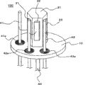
Multi-wavelength semiconductor laser device 100 among Fig. 1 possesses: the discoideus base (stem) 10 that utilizes sheet metal to form; The bottom surface is carried on the counter-base frame 21 of positive hexagonal column of the upper surface of base 10; Be arranged on 3 LD31~33 on counter-base frame 21 sides; Run through base 10 ground settings and with 3 pin terminals (lead pin) 41~43 of the opposed position configuration of knuckle line 21a~21c of counter-base frame 21; And the earth terminal 50 that is connected to base 10.
In addition, the central shaft 10z of base 10 is configured to almost consistent with the center of the semiconductor laser elements that comprises multi-wavelength semiconductor laser device 100 (package) (not having diagram).
Counter-base frame 21 metal materials by high thermal conductivity such as copper alloys form, and its central shaft 21z is set to consistent with the central shaft 10z of base 10.In addition, the knuckle line of side not necessarily will be made seamed edge (edge) shape, can chamfering or rounding.
3 LD31~33 are welded on respectively on 3 adjacent in counter-base frame 21 sides sides, and equal in fact to the distance of each luminous point 31a~33a in order to guarantee from the central shaft 10z of base 10, and LD31~33 are configured in the middle body on each limit.Here, " distance equal in fact " is meant the assembly error that can exist in the optical design to be allowed etc.Also have, each LD31~33 are configured to, the laser that makes each LD31~33 along with the parallel direction emission of central shaft 21z direction of the central shaft 10z and the counter-base frame of base.And the oscillation wavelength of LD31~33 is respectively 780nm wave band (infrared), 650nm wave band (redness), 405nm wave band (bluish violet), is not particularly limited the order of setting.
Earth terminal 50 engages by welding with base 10, and earth terminal 50 is via base 10 and counter-base frame 21, with the n lateral electrode electric connection (not diagram) of LD31~33.
By such formation multi-wavelength semiconductor laser device 100, can make the central shaft 10z of base 10, be between the luminous point 31a~33a of the center of semiconductor laser elements and 3 LD31~33 distance about equally, therefore comprise the Design for optical system of multi-wavelength semiconductor laser device 100 easily.
Particularly, counter-base frame 21 is formed the regular hexagon shape, and the central shaft 10z of central shaft 21z that is configured to make the counter-base frame and discoideus base 10 is almost consistent, therefore makes the distance between the luminous point 31a~33a of the central shaft 10z of base 10 and LD31~33 identical easily.
In addition, 3 LD31~33 all are welded on counter-base frame 21, and the heat that is produced during so LD31~33 actions just can pass through counter-base frame 21 and dispel the heat to the outside effectively.
And, by pin terminals 41~43 being configured in the opposed position of knuckle line 21a~21c with counter-base frame 21, carry out the wire-bonded between pin terminals 41~43 and LD31~33 easily, therefore the cloth line procedures can be significantly shortened compared with conventional art, and multi-wavelength semiconductor laser device 100 can be easily made.
Particularly, by pin terminals 41~43 being set to central shaft 21z rotation symmetry, can carry out wire-bonded more easily with respect to counter-base frame 21.
In addition, in the above-described embodiment, counter-base frame 21 forms positive hexagonal column, but the shape of counter-base frame 21 need not be confined to positive hexagonal column, can adopt positive n corner post (n is the integer more than 3) shape, for example, can form counter-base frame 21 by triangle-section cylinder as shown in Figure 3, and be configured to make the central shaft 10z of the central shaft 21z of counter-base frame and base 10 consistent.By such formation counter-base frame 21, can be with each luminous point 31a~33a of LD31~33 central shaft 10z near base 10, be the center of semiconductor laser elements, therefore can comprise the Design for optical system of multi-wavelength semiconductor laser device 100 easily.
In addition, even counter-base frame 21 is not just polygonal column, as long as can make the central shaft 10z of base 10, promptly the distance between each luminous point 31a~33a of the center of semiconductor laser elements and diode 31~33 equates in fact just can.In addition, the knuckle line of side not necessarily will be made the seamed edge shape, can chamfering or rounding.
According to present embodiment, multi-wavelength semiconductor laser device 100 is possessed: tabular base 10; The bottom surface is carried on the counter-base frame 21 of the column on the base 10; Be arranged on counter-base frame 21 sides and different a plurality of LD31~33 of oscillation wavelength; And run through base 10 ground settings and be configured in pin terminals 41~43 with the opposed position of knuckle line 21a~21c of the side of counter-base frame 21.And the distance that multi-wavelength semiconductor laser device 100 constitutes between the central shaft 10z of each the luminous point 31a~33a that makes a plurality of LD31~33 and base 10 is equal in fact.Like this, just can obtain that optical design is simple, heat dissipation characteristics is good, and the multi-wavelength semiconductor laser device of making easily.
Execution mode 2
About the content of embodiments of the present invention 2, describe with reference to figure 4.In the multi-wavelength semiconductor laser device in the present embodiment, constitute among a plurality of LD one by dual laser.
Multi-wavelength semiconductor laser device 200 possesses in Fig. 4: the discoideus base 10 that utilizes sheet metal to form; The bottom surface is carried on the counter-base frame 22 of triangle-section cylinder shape of the upper surface of this base 10; Be arranged on 2 LD34,35 on counter-base frame 22 sides; Run through base 10 ground settings and be configured in 3 pin terminals 41~43 with the opposed position of counter-base frame 22 knuckle line 22a~22c; And the earth terminal 50 that joins base 10 to.
And the central shaft 10z of base 10 is configured to almost consistent with the center of the semiconductor laser elements that comprises multi-wavelength semiconductor laser device 200 (not having diagram).
In 2 LD34,35, a LD34 is that oscillation wavelength is single wavelength LD of 405nm wave band (bluish violet), and another LD35 can launch the dual wavelength LD that oscillation wavelength is the laser of 780nm wave band (infrared) and 650nm wave band (redness).Again, LD34, LD35 are welded on respectively on 2 sides in counter-base frame 22 sides, and LD34,35 is configured in the middle body on each limit, so that the luminous point 34a of single wavelength LD34 equates in fact the distance of the central shaft 10z of base 10 2 luminous point 35a, the 35b of the distance of the central shaft 10z of base 10 and dual wavelength LD35.In addition, each LD34,35 be configured to make each LD34,35 laser along with the parallel direction emission of central shaft 22z direction of the central shaft 10z and the counter-base frame of base.
In addition, earth terminal 50 and execution mode 1 similarly engage with base 10 by welding, and earth terminal 50 is via base 10 and counter-base frame 22, with LD34,35 n lateral electrode (not illustrating) electric connection.
By such formation multi-wavelength semiconductor laser device 200, can make the central shaft 10z of base 10, be semiconductor laser elements the center to the distance between luminous point 35a, the 35b of the luminous point 34a of single wavelength LD34 and dual wavelength LD35 about equally, therefore comprise the Design for optical system of multi-wavelength semiconductor laser device 200 easily.
Particularly, counter-base frame 22 forms the triangle-section cylinder shape, and the central shaft 10z of central shaft 22z that is configured to make the counter-base frame and discoideus base 10 is set to almost consistent, therefore is more prone to make LD34,35 luminous point 34a, 35a, 35b identical with respect to the distance of the central shaft 10z of base 10.
In addition, 2 LD34,35 all are welded on counter-base frame 22, so the heat that is produced when LD34,35 actions just can pass through counter-base frame 22 and dispel the heat to the outside effectively.
And, by pin terminals 41~43 being configured in the opposed position of knuckle line 22a~22c with counter-base frame 22, make pin terminals 41~43 and LD34,35 wire-bonded become simple, therefore the cloth line procedures can be significantly shortened compared with conventional art, and multi-wavelength semiconductor laser device 200 can be easily made.
Particularly, by pin terminals 41~43 being set to central shaft 22z rotation symmetry, can carry out wire-bonded more easily with respect to counter-base frame 22.
According to present embodiment, multi-wavelength semiconductor laser device 200 is possessed: discoideus base 10; The bottom surface is carried on the counter-base frame 22 of the column on the base 10; Be arranged on counter-base frame 22 sides and the different a plurality of LD34,35 of oscillation wavelength; Run through base 10 ground settings and be configured in pin terminals 41~43 with the opposed position of knuckle line 22a~22c of counter-base frame 22 sides.And the distance that multi-wavelength semiconductor laser device 200 constitutes between the central shaft 10z that makes a plurality of LD34, each luminous point 34a, 35a of 35 and base 10 is equal in fact.Like this, just can obtain that optical design is simple, heat dissipation characteristics is good, and the multi-wavelength semiconductor laser device of making easily.
Execution mode 3
About the content of embodiments of the present invention 3, describe with reference to figure 5.The structure of the multi-wavelength semiconductor laser device in the present embodiment is, constitutes among a plurality of LD one by dual wavelength LD, and by will these a plurality of LD being configured near the knuckle line of counter-base frame, the luminous point that makes each LD is near the assembly center.
In the multi-wavelength semiconductor laser device 300 in the present embodiment of Fig. 5, the dual wavelength LD35 that sends single wavelength LD34 of bluish violet color laser and send red and infrared laser is configured in two sides of the counter-base frame 23 of triangle-section cylinder shape respectively, and LD34,35 is configured near 1 knuckle line 23b.In addition, be arranged to make luminous point 34a, 35a, the 35b of each LD central shaft 10z to base 10, promptly the distance between the center of semiconductor laser elements is almost equal.Except these points, the multi-wavelength semiconductor device 300 in the execution mode 3 has and the identical structure of multi-wavelength semiconductor device 200 in the execution mode 2.
By such formation multi-wavelength semiconductor laser device 300, can make the central shaft 10z of base 10, the center that is semiconductor laser elements is equal in fact to the distance between luminous point 35a, the 35b of the luminous point 34a of single wavelength LD34 and dual wavelength LD35, can make luminous point 34a, the 35a of each LD, the center of the close assembly of 35b in the case, therefore comprise the Design for optical system of multi-wavelength semiconductor laser device 300 more easily.
According to present embodiment, multi-wavelength semiconductor laser device 300 is comprised: discoideus base 10; The bottom surface is carried on the counter-base frame 23 of the column on the base 10; Be arranged on counter-base frame 23 sides and the different a plurality of LD34,35 of oscillation wavelength; Run through base 10 ground settings and be configured in pin terminals 41~43 with the opposed position of knuckle line 23a~23c of counter-base frame 23 sides.And the distance that multi-wavelength semiconductor laser device 300 constitutes between the central shaft 10z that makes a plurality of LD34,35 each luminous point 34a, 35a, 35b and base 10 is equal in fact, and pin terminals 41~43 is the rotation symmetry with respect to the central shaft 23z of counter-base frame 23, and makes LD34,35 luminous point 34a, 35a, the central shaft 10z of the close base 10 of 35b.Like this, just can obtain that optical design is simple, heat dissipation characteristics is good, and the multi-wavelength semiconductor laser device of making easily.
Though no longer describe, but the present invention is not limited to above-mentioned execution mode, in the scope of technological thought of the present invention, has comprised various variation or extended example.
Symbol description:
10 bases; The central shaft of 10z base; 21~23 counter-base framves; 21a~21c, 22a~22c, 23a~23c knuckle line; The central shaft of 21z~23z counter-base frame; 31~35 LD; 31a~35a, 35b luminous point; 41~43 pin terminals; 41a~43a insulator; 50 ground terminals; 100,200,300 multi-wavelength semiconductor laser devices.
Claims (7)
1. multi-wavelength semiconductor laser device is characterized in that comprising:
Tabular base;
The counter-base frame of column, its bottom surface are carried on the above-mentioned base;
A plurality of laser diodes that oscillation wavelength is different are arranged on the side of above-mentioned counter-base frame; And
Pin terminals runs through above-mentioned base ground and is provided with and is configured in the opposed position of knuckle line with above-mentioned counter-base frame side,
The luminous point of above-mentioned a plurality of laser diodes is equal in fact to the distance of the central shaft of above-mentioned base.
2. multi-wavelength semiconductor laser device as claimed in claim 1 is characterized in that: above-mentioned counter-base frame is just polygonal column.
3. multi-wavelength semiconductor laser device as claimed in claim 1 is characterized in that: above-mentioned counter-base frame is the triangle-section cylinder shape.
4. multi-wavelength semiconductor laser device as claimed in claim 1 is characterized in that: above-mentioned pin terminals is the rotation symmetry with respect to the central shaft of above-mentioned counter-base frame.
5. multi-wavelength semiconductor laser device as claimed in claim 1 is characterized in that: the central shaft of above-mentioned counter-base frame is consistent with the central shaft of above-mentioned base.
6. multi-wavelength semiconductor laser device as claimed in claim 1 is characterized in that: at least one in above-mentioned a plurality of laser diodes is dual wavelength laser diode.
7. multi-wavelength semiconductor laser device as claimed in claim 6 is characterized in that: above-mentioned a plurality of laser diodes are configured near the knuckle line of above-mentioned counter-base frame side.
Applications Claiming Priority (2)
| Application Number | Priority Date | Filing Date | Title |
|---|---|---|---|
| JP2009-098949 | 2009-04-15 | ||
| JP2009098949A JP2010251502A (en) | 2009-04-15 | 2009-04-15 | Multi-wavelength semiconductor laser device |
Publications (1)
| Publication Number | Publication Date |
|---|---|
| CN101867157A true CN101867157A (en) | 2010-10-20 |
Family
ID=42958764
Family Applications (1)
| Application Number | Title | Priority Date | Filing Date |
|---|---|---|---|
| CN201010165214A Pending CN101867157A (en) | 2009-04-15 | 2010-04-14 | Multi-wavelength semiconductor laser device |
Country Status (3)
| Country | Link |
|---|---|
| US (1) | US8322879B2 (en) |
| JP (1) | JP2010251502A (en) |
| CN (1) | CN101867157A (en) |
Cited By (3)
| Publication number | Priority date | Publication date | Assignee | Title |
|---|---|---|---|---|
| CN104852274A (en) * | 2014-02-13 | 2015-08-19 | 三菱电机株式会社 | Semiconductor laser light source |
| CN112582874A (en) * | 2019-09-29 | 2021-03-30 | 山东华光光电子股份有限公司 | Composite laser for laser light moxibustion and packaging method |
| WO2021098841A1 (en) * | 2019-11-21 | 2021-05-27 | 深圳市中光工业技术研究院 | Laser light source |
Families Citing this family (6)
| Publication number | Priority date | Publication date | Assignee | Title |
|---|---|---|---|---|
| GB2477458B (en) * | 2009-06-09 | 2012-03-07 | Mitsubishi Electric Corp | Multi-wavelength semiconductor laser device |
| JP5522977B2 (en) | 2009-06-09 | 2014-06-18 | 三菱電機株式会社 | Multi-wavelength semiconductor laser device |
| US9927611B2 (en) | 2010-03-29 | 2018-03-27 | Soraa Laser Diode, Inc. | Wearable laser based display method and system |
| JP6722474B2 (en) * | 2016-03-09 | 2020-07-15 | フォトンリサーチ株式会社 | Multi-wavelength laser light source module and multi-wavelength laser light source module with multiplexer |
| DE102018009383A1 (en) * | 2018-11-30 | 2020-06-04 | Diehl Defence Gmbh & Co. Kg | Method for manufacturing a multi-beam laser |
| DE102018009384B4 (en) * | 2018-11-30 | 2022-01-20 | Diehl Defence Gmbh & Co. Kg | Laser Detector System |
Citations (5)
| Publication number | Priority date | Publication date | Assignee | Title |
|---|---|---|---|---|
| US5648977A (en) * | 1994-10-11 | 1997-07-15 | Mitsubishi Denki Kabushiki Kaisha | Laser array device and method of fabricating the device |
| US5668822A (en) * | 1994-08-05 | 1997-09-16 | Mitsubishi Denki Kabushiki Kaisha | Integrated semiconductor laser device |
| JP3240794B2 (en) * | 1993-11-25 | 2001-12-25 | 株式会社デンソー | Semiconductor laser |
| CN1677781A (en) * | 2004-03-30 | 2005-10-05 | 三洋电机株式会社 | Semiconductor laser apparatus |
| CN1838494A (en) * | 2005-03-25 | 2006-09-27 | 三洋电机株式会社 | Semiconductor laser apparatus and optical pickup apparatus |
Family Cites Families (5)
| Publication number | Priority date | Publication date | Assignee | Title |
|---|---|---|---|---|
| JPS63287085A (en) * | 1987-05-19 | 1988-11-24 | Omron Tateisi Electronics Co | Multi-beam light source |
| JPH11186669A (en) | 1997-12-22 | 1999-07-09 | Victor Co Of Japan Ltd | Semiconductor laser device |
| JPH11186658A (en) * | 1997-12-24 | 1999-07-09 | Victor Co Of Japan Ltd | Semiconductor laser device |
| JP2006059471A (en) | 2004-08-20 | 2006-03-02 | Sony Corp | Laser emitting apparatus and optical head |
| JP2007115724A (en) * | 2005-10-18 | 2007-05-10 | Matsushita Electric Ind Co Ltd | Semiconductor laser device |
-
2009
- 2009-04-15 JP JP2009098949A patent/JP2010251502A/en active Pending
-
2010
- 2010-04-02 US US12/753,136 patent/US8322879B2/en active Active
- 2010-04-14 CN CN201010165214A patent/CN101867157A/en active Pending
Patent Citations (5)
| Publication number | Priority date | Publication date | Assignee | Title |
|---|---|---|---|---|
| JP3240794B2 (en) * | 1993-11-25 | 2001-12-25 | 株式会社デンソー | Semiconductor laser |
| US5668822A (en) * | 1994-08-05 | 1997-09-16 | Mitsubishi Denki Kabushiki Kaisha | Integrated semiconductor laser device |
| US5648977A (en) * | 1994-10-11 | 1997-07-15 | Mitsubishi Denki Kabushiki Kaisha | Laser array device and method of fabricating the device |
| CN1677781A (en) * | 2004-03-30 | 2005-10-05 | 三洋电机株式会社 | Semiconductor laser apparatus |
| CN1838494A (en) * | 2005-03-25 | 2006-09-27 | 三洋电机株式会社 | Semiconductor laser apparatus and optical pickup apparatus |
Cited By (5)
| Publication number | Priority date | Publication date | Assignee | Title |
|---|---|---|---|---|
| CN104852274A (en) * | 2014-02-13 | 2015-08-19 | 三菱电机株式会社 | Semiconductor laser light source |
| CN104852274B (en) * | 2014-02-13 | 2018-11-27 | 三菱电机株式会社 | Semiconductor laser light resource |
| CN112582874A (en) * | 2019-09-29 | 2021-03-30 | 山东华光光电子股份有限公司 | Composite laser for laser light moxibustion and packaging method |
| CN112582874B (en) * | 2019-09-29 | 2021-10-01 | 山东华光光电子股份有限公司 | Composite laser for laser light moxibustion and packaging method |
| WO2021098841A1 (en) * | 2019-11-21 | 2021-05-27 | 深圳市中光工业技术研究院 | Laser light source |
Also Published As
| Publication number | Publication date |
|---|---|
| US20100265702A1 (en) | 2010-10-21 |
| US8322879B2 (en) | 2012-12-04 |
| JP2010251502A (en) | 2010-11-04 |
Similar Documents
| Publication | Publication Date | Title |
|---|---|---|
| CN101867157A (en) | Multi-wavelength semiconductor laser device | |
| US8687668B2 (en) | Multi-wavelength semiconductor laser device | |
| CN100502177C (en) | Two-beam semiconductor laser apparatus | |
| US20070177648A1 (en) | Multiple wavelengths semiconductor laser device | |
| JP2005116700A (en) | Semiconductor laser | |
| JP4583128B2 (en) | Semiconductor laser device | |
| JP2007035854A (en) | Semiconductor laser array and semiconductor laser device | |
| JP2002109774A (en) | Optical pickup | |
| JP5799727B2 (en) | Multi-wavelength semiconductor laser device and method for manufacturing multi-wavelength semiconductor laser device | |
| JP3980037B2 (en) | Semiconductor device | |
| JP2008021754A (en) | Frame package type semiconductor laser device | |
| JP6221733B2 (en) | Semiconductor laser | |
| JP4204581B2 (en) | Semiconductor laser device | |
| JP5216807B2 (en) | Semiconductor laser device | |
| CN100373717C (en) | Lead frame for semiconductor element and semiconductor device using same | |
| GB2477458A (en) | Multi-wavelength semiconductor laser device | |
| JP2013016585A (en) | Multi-wavelength semiconductor laser device | |
| JP2006013551A (en) | Semiconductor laser apparatus | |
| JP2021048234A (en) | Semiconductor laser light source device | |
| JP2010183111A5 (en) | ||
| JP2006049767A (en) | Semiconductor laser device and optical pick-up device | |
| JP2006295223A (en) | Semiconductor device | |
| JP2008016714A (en) | Frame package type semiconductor laser device | |
| JP2013080781A (en) | Multi-wavelength semiconductor laser device | |
| JP2005064162A (en) | Semiconductor laser equipment loading frame, semiconductor laser equipment, manufacturing method thereof and optical pickup equipment |
Legal Events
| Date | Code | Title | Description |
|---|---|---|---|
| C06 | Publication | ||
| PB01 | Publication | ||
| C10 | Entry into substantive examination | ||
| SE01 | Entry into force of request for substantive examination | ||
| C12 | Rejection of a patent application after its publication | ||
| RJ01 | Rejection of invention patent application after publication |
Application publication date: 20101020 |