CN101699552B - Grid output control method and corresponding grid pulse modulator - Google Patents
Grid output control method and corresponding grid pulse modulator Download PDFInfo
- Publication number
- CN101699552B CN101699552B CN2009102119160A CN200910211916A CN101699552B CN 101699552 B CN101699552 B CN 101699552B CN 2009102119160 A CN2009102119160 A CN 2009102119160A CN 200910211916 A CN200910211916 A CN 200910211916A CN 101699552 B CN101699552 B CN 101699552B
- Authority
- CN
- China
- Prior art keywords
- control signal
- gate
- adjusted
- angle
- gate control
- Prior art date
- Legal status (The legal status is an assumption and is not a legal conclusion. Google has not performed a legal analysis and makes no representation as to the accuracy of the status listed.)
- Active
Links
- 238000000034 method Methods 0.000 title claims abstract description 25
- 238000007599 discharging Methods 0.000 claims description 3
- 230000007704 transition Effects 0.000 claims 3
- 230000007547 defect Effects 0.000 abstract description 6
- 238000010586 diagram Methods 0.000 description 11
- 239000000758 substrate Substances 0.000 description 4
- 238000009966 trimming Methods 0.000 description 3
- 238000005516 engineering process Methods 0.000 description 2
- 230000005540 biological transmission Effects 0.000 description 1
- 239000004973 liquid crystal related substance Substances 0.000 description 1
- 238000012986 modification Methods 0.000 description 1
- 230000004048 modification Effects 0.000 description 1
Images


Landscapes
- Control Of Indicators Other Than Cathode Ray Tubes (AREA)
- Transforming Electric Information Into Light Information (AREA)
Abstract
本发明公开了一种栅极输出控制方法及相应的栅极脉冲调制器,该栅极输出控制方法包括:提供栅极控制信号;提供削角控制信号对栅极控制信号进行削角调制而产生具有削角的栅极控制信号;对具有削角的栅极控制信号进行调制处理而得到调整后的栅极控制信号;以及输出调整后的栅极控制信号至多个栅极驱动集成电路。其中调整后的栅极控制信号的下降缘包括削角变化期及垂直变化期,在削角变化期内,调整后的栅极控制信号先以第一斜率变化至预定电压,再以第二斜率变直至垂直变化期,且调整后的栅极控制信号在垂直变化期内以接近垂直的方式变化电压。通过本发明可有效克服现有技术中存在的垂直面亮度不均的缺陷。
The present invention discloses a gate output control method and a corresponding gate pulse modulator, the gate output control method comprising: providing a gate control signal; providing a chamfer control signal to chamfer and modulate the gate control signal to generate a chamfered gate control signal; modulating the chamfered gate control signal to obtain an adjusted gate control signal; and outputting the adjusted gate control signal to a plurality of gate drive integrated circuits. The falling edge of the adjusted gate control signal comprises a chamfered change period and a vertical change period, during which the adjusted gate control signal first changes to a predetermined voltage with a first slope, and then changes to a vertical change period with a second slope, and the adjusted gate control signal changes voltage in a nearly vertical manner during the vertical change period. The present invention can effectively overcome the defect of uneven vertical surface brightness existing in the prior art.
Description
技术领域 technical field
本发明是有关于显示技术领域,且特别是有关于一种栅极输出控制方法及相应的栅极脉冲调制器。The present invention relates to the field of display technology, and in particular to a grid output control method and a corresponding grid pulse modulator.
背景技术 Background technique
平面显示器(例如,液晶显示器)具有高画质、体积小、重量轻及应用范围广等优点,因此被广泛地应用于行动电话、笔记型电脑、桌上型显示器以及电视等各种消费性电子产品中,并已经逐渐取代传统的阴极射线管显示器而成为显示器的主流。Flat panel displays (such as liquid crystal displays) have the advantages of high image quality, small size, light weight and wide application range, so they are widely used in various consumer electronics such as mobile phones, notebook computers, desktop monitors and televisions. Products, and has gradually replaced the traditional cathode ray tube display and become the mainstream of the display.
参见图1,其示出现有技术中的一种平面显示器的结构框图。如图1所示,平面显示器100包括显示基板110、印刷电路板120及多个软性电路板130。显示基板110上设置有多个栅极驱动集成电路GD1及GD2、多个源极驱动集成电路(图未示)以及显示区块111及112。栅极驱动集成电路GD1及GD2分别控制显示区块111及112并透过阵列上导线(WOA,Wire-On-Array)彼此串联耦接。印刷电路板120透过软性电路板130与显示基板110相电性耦接,其上设置有时序控制器140及栅极脉冲调制器150。时序控制器140向栅极驱动集成电路GD1及GD2提供栅极输出使能信号YOE_Y1及YOE_Y2,并输出栅极控制信号VGH1及削角控制信号YV1C至栅极脉冲调制器150以使栅极脉冲调制器150输出调整后的栅极控制信号VGH至栅极驱动集成电路GD1及GD2。然后,调整后的栅极控制信号VGH与栅极输出使能信号YOE_Y1及YOE_Y2相配合,产生相应的栅极驱动信号Gate Pulse_Y1及GatePulse_Y2。Referring to FIG. 1 , it shows a structural block diagram of a flat panel display in the prior art. As shown in FIG. 1 , the
参见图2,其绘示出现有技术中的一种栅极脉冲调制器的示意图。如图2所示,栅极脉冲调制器150为一个脉冲宽度调制电路(PWM IC),其包括栅极控制信号端151、削角控制信号端152、放电电路153及输出端154。栅极控制信号端151接收栅极控制信号VGH1,削角控制信号端152接收削角控制信号YV1C,栅极脉冲调制器150根据削角控制信号YV1C来决定是否利用放电电路153对栅极控制信号VGH1进行放电从而产生调整后的栅极控制信号VGH,并利用输出端154输出至栅极驱动集成电路GD1及GD2。Referring to FIG. 2 , it shows a schematic diagram of a gate pulse modulator in the prior art. As shown in FIG. 2 , the
参见图3,其绘示为图2所示的栅极脉冲调制器的栅极控制信号VGH1、削角控制信号YV1C及调整后的栅极控制信号VGH以及图1所示的栅极输出使能信号YOE_Y1及YOE_Y2、栅极驱动信号Gate Pulse_Y1及Gate Pulse_Y2的时序图。如图3所示,栅极脉冲调制器150所输出的调整后的栅极控制信号VGH为一个具有削角的栅极控制信号,其以某一斜率下降至某一电压后,再以垂直的方式变化电压。此外,由于阵列上导线的阻抗较大,因此调整后的栅极控制信号VGH及栅极输出使能信号YOE_Y1及YOE_Y2在传输至栅极驱动集成电路GD1及GD2的过程中因导线衰减而产生波形变化,使得驱动栅极驱动集成电路GD1及GD2的栅极驱动信号Gate Pulse_Y1及GatePulse_Y2的削角截止电压V1及V2之间存在电压落差ΔV0,进而导致显示区块111及112的亮度有所差异而产生交界的水平淡线,亦即存在垂直面亮度不均的缺陷。Referring to FIG. 3 , it shows the gate control signal VGH1 , the chamfering control signal YV1C and the adjusted gate control signal VGH of the gate pulse modulator shown in FIG. 2 , and the gate output enable shown in FIG. 1 Timing diagram of signals YOE_Y1 and YOE_Y2, gate drive signals Gate Pulse_Y1 and Gate Pulse_Y2. As shown in FIG. 3 , the adjusted gate control signal VGH output by the
发明内容 Contents of the invention
本发明的目的就是在提供一种栅极输出控制方法,以有效克服现有技术中平面显示器垂直面亮度不均的缺陷。The purpose of the present invention is to provide a gate output control method to effectively overcome the defect of uneven brightness in the vertical plane of the flat panel display in the prior art.
本发明的再一目的是提供一种栅极脉冲调制器,以有效克服现有技术中平面显示器垂直面亮度不均的缺陷。Another object of the present invention is to provide a grid pulse modulator to effectively overcome the defect of uneven brightness in the vertical plane of the flat panel display in the prior art.
本发明提出一种适用于平面显示器的栅极输出控制方法,平面显示器包括第一栅极驱动集成电路及第二栅极驱动集成电路。栅极输出控制方法包括:提供栅极控制信号;提供削角控制信号对栅极控制信号进行削角调制而产生具有削角的栅极控制信号;对具有削角的栅极控制信号进行调制处理而得到调整后的栅极控制信号,其中调整后的栅极控制信号的下降缘包括削角变化期及垂直变化期,在削角变化期内,调整后的栅极控制信号先以第一斜率变化至预定电压,再以第二斜率变直至垂直变化期,且调整后的栅极控制信号在垂直变化期内以接近垂直的方式变化电压;以及输出调整后的栅极控制信号至第一栅极驱动集成电路及第二栅极驱动集成电路,以依序控制第一栅极驱动集成电路及第二栅极驱动集成电路的栅极输出。The invention proposes a gate output control method suitable for a flat panel display, and the flat panel display includes a first gate driving integrated circuit and a second gate driving integrated circuit. The grid output control method includes: providing a grid control signal; providing a chamfered control signal to modulate the grid control signal to generate a grid control signal with a chamfered angle; and performing modulation processing on the chamfered grid control signal And the adjusted gate control signal is obtained, wherein the falling edge of the adjusted gate control signal includes a chamfering change period and a vertical change period, and in the chamfering change period, the adjusted gate control signal first slopes Change to a predetermined voltage, and then change to a vertical change period with a second slope, and the adjusted gate control signal changes the voltage in a nearly vertical manner during the vertical change period; and output the adjusted gate control signal to the first gate A pole driving integrated circuit and a second gate driving integrated circuit are used to sequentially control the gate output of the first gate driving integrated circuit and the second gate driving integrated circuit.
在本发明的较佳实施例中,上述的提供削角控制信号对栅极控制信号进行削角调制而产生具有削角的栅极控制信号的步骤包括:根据削角控制信号来决定是否利用第一放电电路对栅极控制信号进行放电。In a preferred embodiment of the present invention, the step of providing the angle-cutting control signal to perform angle-cutting modulation on the gate control signal to generate a gate control signal with a cut-off angle includes: determining whether to use the first A discharge circuit discharges the gate control signal.
在本发明的较佳实施例中,上述的调整后的栅极控制信号的第二斜率约为0以使调整后的栅极控制信号持续维持于预定电压附近。In a preferred embodiment of the present invention, the second slope of the adjusted gate control signal is about 0 so that the adjusted gate control signal is maintained near the predetermined voltage.
在本发明的较佳实施例中,上述的对具有削角的栅极控制信号进行调制处理而得到调整后的栅极控制信号的步骤是利用削角定压电路而实现。其中上述的步骤包括:藉由预定电压源提供预定电压;以及于削角变化期内,当具有削角的栅极控制信号小于预定电压时,使预定电压源提供的预定电压作为调整后的栅极控制信号。In a preferred embodiment of the present invention, the above step of modulating the gate control signal with a chamfered angle to obtain the adjusted gate control signal is realized by using a chamfered angle constant voltage circuit. Wherein the above-mentioned steps include: providing a predetermined voltage by a predetermined voltage source; and during the angle-cutting variation period, when the gate control signal with a cut-off angle is less than a predetermined voltage, using the predetermined voltage provided by the predetermined voltage source as the adjusted grid pole control signal.
在本发明的较佳实施例中,上述的对具有削角的栅极控制信号进行调制处理而得到调整后的栅极控制信号的步骤亦可包括:根据控制信号来决定是否利用第二放电电路对具有削角的栅极控制信号进行进一步放电,从而在削角变化期内使调整后的栅极控制信号的第二斜率约为0以使调整后的栅极控制信号持续维持于预定电压附近。其中,当利用第二放电电路对具有削角的栅极控制信号进行进一步放电时,第一放电电路继续进行放电。或者,当利用第二放电电路对具有削角的栅极控制信号进行进一步放电时,第一放电电路停止放电。In a preferred embodiment of the present invention, the step of modulating the gate control signal with chamfered angles to obtain the adjusted gate control signal may also include: deciding whether to use the second discharge circuit according to the control signal further discharging the gate control signal with the chamfered angle, so that the second slope of the adjusted gate control signal is about 0 during the chamfered angle change period so that the adjusted gate control signal is continuously maintained near the predetermined voltage . Wherein, when the second discharge circuit is used to further discharge the gate control signal with chamfered angles, the first discharge circuit continues to discharge. Alternatively, when the second discharge circuit is used to further discharge the chamfered gate control signal, the first discharge circuit stops discharging.
在本发明的较佳实施例中,上述的栅极输出控制方法进一步包括:分别输出第一使能信号及第二使能信号至第一栅极驱动集成电路及第二栅极驱动集成电路以与调整后的栅极控制信号配合而产生第一栅极驱动信号及第二栅极驱动信号,其中第一栅极驱动信号及第二栅极驱动信号的削角截止电压相同。In a preferred embodiment of the present invention, the above gate output control method further includes: respectively outputting the first enable signal and the second enable signal to the first gate drive integrated circuit and the second gate drive integrated circuit to Cooperating with the adjusted gate control signal to generate a first gate drive signal and a second gate drive signal, wherein the cut-off voltages of the first gate drive signal and the second gate drive signal are the same.
本发明还提出一种适用于平面显示器的栅极脉冲调制器。平面显示器包括第一栅极驱动集成电路及第二栅极驱动集成电路,栅极脉冲调制器包括栅极控制信号端、削角控制信号端、第一放电电路、削角输出端、削角定压电路及输出端。栅极控制信号端用以接收栅极控制信号,削角控制信号端用以接收削角控制信号,削角输出端用以输出具有削角的栅极控制信号,而输出端用以输出调整后的栅极控制信号至第一栅极驱动集成电路及第二栅极驱动集成电路。其中,栅极脉冲调制器依据削角控制信号以决定是否利用第一放电电路对栅极控制信号进行放电而产生具有削角的栅极控制信号,且利用削角定压电路对具有削角的栅极控制信号进行调制处理而得到调整后的栅极控制信号。调整后的栅极控制信号的下降缘包括削角变化期及垂直变化期,该削角变化期内,调整后的栅极控制信号先以第一斜率变化至预定电压,再以第二斜率变化直至垂直变化期,且调整后的栅极控制信号在垂直变化期内以接近垂直的方式变化电压。The invention also proposes a gate pulse modulator suitable for a flat panel display. The flat panel display includes a first gate drive integrated circuit and a second gate drive integrated circuit, and the gate pulse modulator includes a gate control signal terminal, an angle trimming control signal end, a first discharge circuit, an angle trimming output terminal, and an angle trimming output terminal. Voltage circuit and output terminal. The grid control signal end is used to receive the grid control signal, the angle-cutting control signal end is used to receive the angle-cutting control signal, the angle-cutting output terminal is used to output the grid control signal with the angle-cutting, and the output terminal is used to output the adjusted The gate control signal is sent to the first gate driving integrated circuit and the second gate driving integrated circuit. Wherein, the gate pulse modulator determines whether to use the first discharge circuit to discharge the gate control signal to generate a gate control signal with a chamfered angle according to the chamfered angle control signal, and uses the chamfered angle constant voltage circuit to discharge the gate control signal with a chamfered angle. The gate control signal is modulated to obtain an adjusted gate control signal. The falling edge of the adjusted gate control signal includes a chamfering change period and a vertical change period. During the chamfering change period, the adjusted gate control signal first changes to a predetermined voltage with a first slope, and then changes with a second slope until the vertical change period, and the adjusted gate control signal changes the voltage in a nearly vertical manner during the vertical change period.
在本发明的较佳实施例中,上述的削角定压电路包括预定电压源以及二极管。预定电压源提供预定电压,而二极管的正端电性耦接于预定电压,其负端电性耦接于削角输出端以接收具有削角的栅极控制信号。其中,在削角变化期内,当具有削角的栅极控制信号小于预定电压时,使预定电压源提供的预定电压作为调整后的栅极控制信号。In a preferred embodiment of the present invention, the above-mentioned chamfering constant voltage circuit includes a predetermined voltage source and a diode. The predetermined voltage source provides a predetermined voltage, and the positive end of the diode is electrically coupled to the predetermined voltage, and the negative end of the diode is electrically coupled to the clipped output end to receive the clipped gate control signal. Wherein, during the angle-cutting change period, when the gate control signal with the cut-off angle is less than a predetermined voltage, the predetermined voltage provided by the predetermined voltage source is used as the adjusted gate control signal.
在本发明的较佳实施例中,上述的削角定压电路亦可包括开关及第二放电电路。开关用以接收控制信号,而第二放电电路电性耦接于开关。其中,栅极脉冲调制器根据控制信号来决定是否利用第二放电电路对具有削角的栅极控制信号进行进一步放电,从而在削角变化期内使调整后的栅极控制信号的第二斜率约为0以使调整后的栅极控制信号持续维持于预定电压附近。In a preferred embodiment of the present invention, the above-mentioned chamfering constant voltage circuit may also include a switch and a second discharge circuit. The switch is used for receiving the control signal, and the second discharge circuit is electrically coupled to the switch. Wherein, the gate pulse modulator determines whether to use the second discharge circuit to further discharge the gate control signal with the chamfered angle according to the control signal, so that the second slope of the adjusted gate control signal can be adjusted during the chamfered angle change period It is about 0 so that the adjusted gate control signal can be kept near the predetermined voltage.
本发明是藉由使调整后的栅极控制信号在削角变化期内下降至预定电压后能够持续维持在预定电压附近,使得用于控制不同栅极驱动集成电路的栅极驱动信号具有相同的削角截止电压,进而使得控制各个栅极驱动集成电路的栅极驱动信号之间不存在电压落差;因此本发明可有效克服现有技术中存在的垂直面亮度不均的缺陷。The present invention keeps the adjusted gate control signal close to the predetermined voltage after falling to the predetermined voltage during the chamfering change period, so that the gate drive signals used to control different gate drive integrated circuits have the same The cut-off voltage is cut off, so that there is no voltage drop between the gate drive signals controlling each gate drive integrated circuit; therefore, the present invention can effectively overcome the defect of uneven brightness in the vertical plane existing in the prior art.
为让本发明的上述和其他目的、特征和优点能更明显易懂,下面结合实施例和附图,作详细说明如下。In order to make the above and other objects, features and advantages of the present invention more comprehensible, the following will be described in detail in conjunction with the embodiments and accompanying drawings.
附图说明 Description of drawings
图1为现有技术中一种平面显示器的结构框图;Fig. 1 is a structural block diagram of a flat panel display in the prior art;
图2为现有技术中一种栅极脉冲调制器的示意图;2 is a schematic diagram of a grid pulse modulator in the prior art;
图3为图2所示的栅极脉冲调制器的栅极控制信号、削角控制信号及调整后的栅极控制信号以及图1所示的栅极输出使能信号、栅极驱动信号的时序图;Fig. 3 is the timing sequence of the gate control signal, chamfering control signal and adjusted gate control signal of the gate pulse modulator shown in Fig. 2 and the gate output enable signal and gate drive signal shown in Fig. 1 picture;
图4为本发明一实施例所揭示的栅极脉冲调制器的示意图;FIG. 4 is a schematic diagram of a grid pulse modulator disclosed by an embodiment of the present invention;
图5为本发明一实施例所揭示的栅极输出控制方法的各种信号的时序图。FIG. 5 is a timing diagram of various signals of the gate output control method disclosed by an embodiment of the present invention.
图6为本发明另一实施例所揭示的栅极脉冲调制器的示意图;FIG. 6 is a schematic diagram of a gate pulse modulator disclosed in another embodiment of the present invention;
图7为本发明另一实施例所揭示的栅极输出控制方法的各种信号的时序图。FIG. 7 is a timing diagram of various signals of a gate output control method disclosed by another embodiment of the present invention.
主要元件符号说明:Description of main component symbols:
100:平面显示器100: flat panel display
110:显示基板110: display substrate
111、112:显示区块111, 112: display blocks
120:印刷电路板120: printed circuit board
130:软性电路板130: flexible circuit board
140:时序控制器140: timing controller
150、200、300:栅极脉冲调制器150, 200, 300: Gate pulse modulator
151、210:栅极控制信号端151, 210: gate control signal terminal
152、220:削角控制信号端152, 220: chamfering control signal terminal
153、240、340、352:放电电路153, 240, 340, 352: discharge circuit
154、260:输出端154, 260: output terminal
230:削角输出端230: chamfer output
250、350:削角定压电路250, 350: chamfering constant voltage circuit
2401、3521:电阻2401, 3521: resistance
2402:放电端2402: discharge terminal
251:二极管251: diode
252:预定电压源252: Predetermined voltage source
280、380:削角变化期280, 380: Changing period of chamfering
281、381:第一斜率281, 381: first slope
282、382:第二斜率282, 382: second slope
290、390:垂直变化期290, 390: vertical change period
351:开关351: switch
GD1、GD2:栅极驱动集成电路GD1, GD2: gate drive integrated circuits
VGH1:栅极控制信号VGH1: gate control signal
YV1C:削角控制信号YV1C: chamfering control signal
VGH2:具有削角的栅极控制信号VGH2: Gate control signal with chamfering
VGH:调整后的栅极控制信号VGH: adjusted gate control signal
Vfix:预定电压Vfix: predetermined voltage
YOE_Y1、YOE_Y2:栅极输出使能信号YOE_Y1, YOE_Y2: gate output enable signal
Gate Pulse_Y1、Gate Pulse_Y2:栅极驱动信号Gate Pulse_Y1, Gate Pulse_Y2: gate drive signal
V1、V2:栅极驱动信号的削角截止电压V1, V2: cut-off cut-off voltage of gate drive signal
ΔV:栅极驱动信号的削角截止电压之间的电压落差ΔV: The voltage drop between the chamfered cut-off voltage of the gate drive signal
YV1C2:控制信号YV1C2: control signal
具体实施方式 Detailed ways
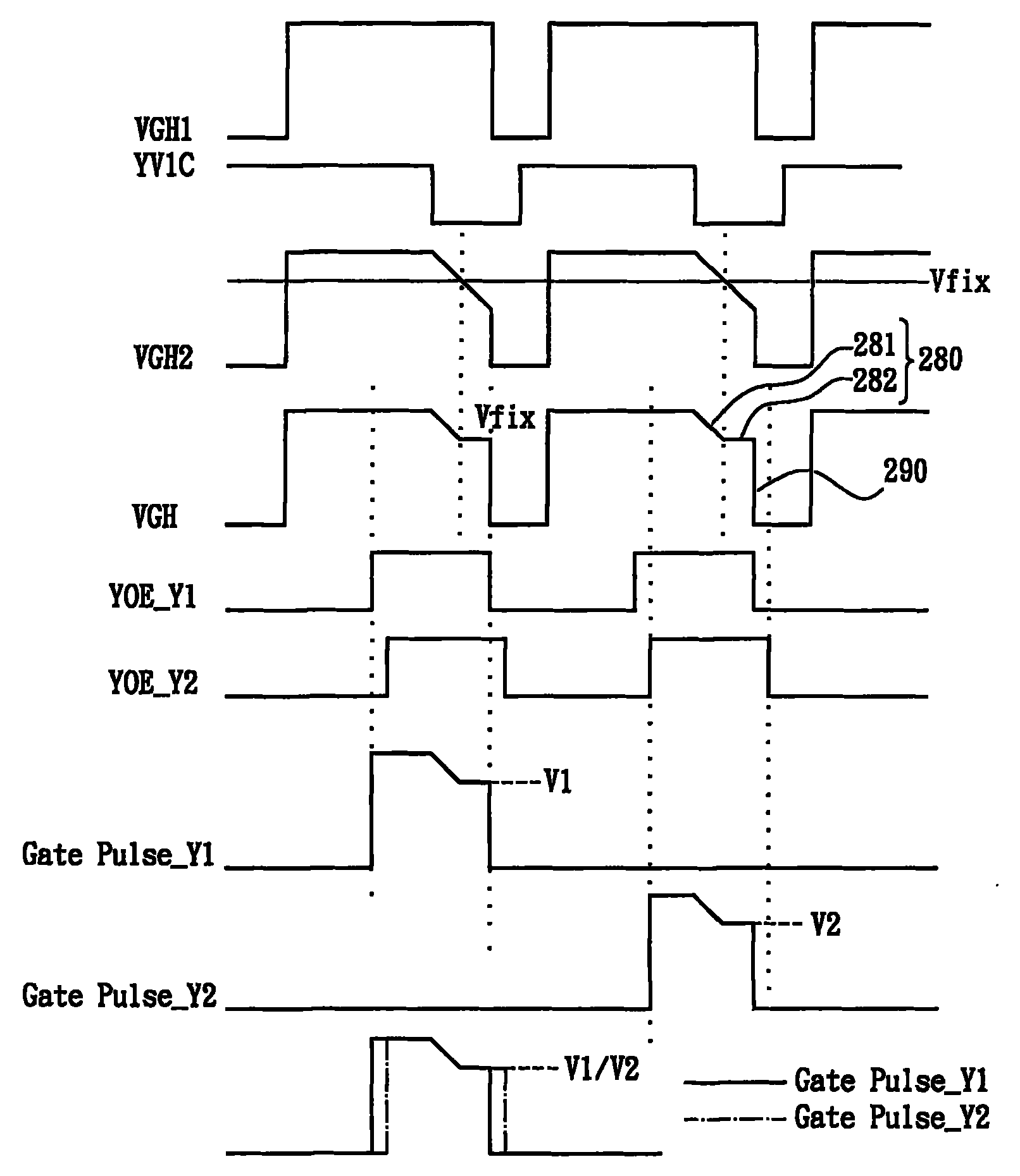
下面将结合图1、图4及图5具体描述本发明一实施例所揭示的一种栅极脉冲调制器及相应的栅极输出控制方法调制,其中图4为本发明实施例所揭示的栅极脉冲调制器的示意图,而图5为本发明实施例所揭示的栅极输出控制方法的各种信号的时序图。本实施例所揭示的栅极脉冲调制器200适用于图1所示的具有栅极驱动集成电路GD1及GD2的平面显示器100,平面显示器100的结构配置可参见上文,在此不再赘述。如图4所示,本实施例所揭示的栅极脉冲调制器200包括栅极控制信号端210、削角控制信号端220、削角输出端230、放电电路240、削角定压电路250及输出端260。A gate pulse modulator disclosed by an embodiment of the present invention and the corresponding gate output control method modulation will be described in detail below with reference to FIG. 1, FIG. 4 and FIG. 5, wherein FIG. 5 is a timing diagram of various signals of the gate output control method disclosed in the embodiment of the present invention. The
请一并参阅图1及图4、图5,栅极控制信号端210接收栅极控制信号VGH1,削角控制信号端220接收削角控制信号YV1C,栅极脉冲调制器200依据削角控制信号YV1C以决定是否利用放电电路240对栅极控制信号VGH1进行放电而于削角输出端230处产生具有削角的栅极控制信号VGH2。放电电路240包括电阻2401,其电性耦接于放电端2402与地之间。其中,具有削角的栅极控制信号VGH2与图2及图3所示的调整后的栅极控制信号VGH相同,此技术为本领域技术人员所熟知,在此不再赘述。Please refer to FIG. 1, FIG. 4, and FIG. 5 together. The grid
削角定压电路250对具有削角的栅极控制信号VGH2进行调制处理而得到调整后的栅极控制信号VGH,其中,调整后的栅极控制信号VGH的下降缘包括削角变化期280及垂直变化期290。在削角变化期280内,调整后的栅极控制信号VGH先以第一斜率281变化至预定电压Vfix,然后再以第二斜率282变化至垂直变化期290,且调整后的栅极控制信号VGH在垂直变化期290内以接近垂直的方式变化电压。The angle-cutting and constant-
在本实施例中,调整后的栅极控制信号VGH的第二斜率为0以使调整后的栅极控制信号VGH持续维持于预定电压Vfix。具体地,本实施例的削角定压电路250包括二极管251及预定电压源252。二极管251的正端电性耦接于预定电压源252以接收预定电压源252所提供的预定电压Vfix,而二极管251的负端电性耦接于削角输出端240以接收具有削角的栅极控制信号VGH2。在削角变化期280内,当具有削角的栅极控制信号VGH2大于预定电压Vfix时,二极管251截止,此时栅极脉冲调制器200的输出端260输出具有削角的栅极控制信号VGH2以作为调整后的栅极控制信号VGH;当具有削角的栅极控制信号VGH2小于预定电压Vfix时,二极管251导通,此时栅极脉冲调制器200的输出端260输出预定电压源252所提供的预定电压Vfix以作为调整后的栅极控制信号VGH。因此,本实施例的削角定压电路250可使调整后的栅极控制信号VGH的第二斜率为0从而使调整后的栅极控制信号VGH持续维持于预定电压Vfix。In this embodiment, the second slope of the adjusted gate control signal VGH is 0 so that the adjusted gate control signal VGH is continuously maintained at the predetermined voltage Vfix. Specifically, the angle-cutting
调整后的栅极控制信号VGH然后输出至图1所示的平面显示器100的栅极驱动集成电路GD1及GD2,其与分别输入至栅极驱动集成电路GD1及GD2的使能信号YOE_Y1及YOE_Y2相配合从而产生相应的栅极驱动信号GatePulse_Y1及Gate Pulse_Y2。如图5所示,由于调整后的栅极控制信号VGH在削角变化期280内,其下降至预定电压Vfix后以其第二斜率为0的方式持续维持于预定电压Vfix,因此栅极驱动信号Gate Pulse_Y1及Gate Pulse_Y2的削角截止电压V1及V2相同,其均维持在预定电压Vfix,即V1=V2=Vfix。也就是说,栅极驱动信号Gate Pulse_Y1及Gate Pulse_Y2的削角截止电压V1及V2之间不存在电压落差,亦即V1-V2=ΔV=0。The adjusted gate control signal VGH is then output to the gate driving integrated circuits GD1 and GD2 of the
请参阅图6及图7,其绘示出本发明另一实施例所揭示的一种栅极脉冲调制器及相应的栅极输出控制方法的示意图。如图6、图7所示,本实施例的栅极脉冲调制器300与图4所示的栅极脉冲调制器200相似,其不同在于:本实施例的栅极脉冲调制器300的削角定压电路350包括开关351及电性耦接于开关351的放电电路352。开关351接收控制信号YV1C2,并依据控制信号YV1C2来决定是否利用放电电路352对具有削角的栅极控制信号VGH2进行进一步地放电,从而于削角变化期380内使调整后的栅极控制信号VGH以第二斜率382变化至垂直变化期390。放电电路352包括电阻3521,其电性耦接于开关351及地之间。通过调整电阻3521的电阻值大小,可更改第二斜率的大小。在本实施例中,可通过设定电阻3521的电阻值从而使第二斜率约为0以使调整后的栅极控制信号持续维持于预定电压Vfix附近。也就是说,本实施例的栅极脉冲调制器300是利用放电电路340及350而进行二次放电操作,从而使调整后的栅极控制信号VGH先以第一斜率381进行变化,再以趋近于0的第二斜率382进行变化以使调整后的栅极控制信号VGH持续维持于预定电压Vfix附近。Please refer to FIG. 6 and FIG. 7 , which illustrate a schematic diagram of a gate pulse modulator and a corresponding gate output control method disclosed in another embodiment of the present invention. As shown in Fig. 6 and Fig. 7, the
此外,如图7所示,在本实施例中,在利用放电电路352对具有削角的栅极控制信号VGH2进行放电的时候,放电电路340同时继续对具有削角的栅极控制信号VGH2进行放电。当然,本领域技术人员可知,本发明亦可在放电电路352对具有削角的栅极控制信号VGH2进行放电的时候,放电电路340停止其放电动作,仅由放电电路352进行放电动作。In addition, as shown in FIG. 7 , in this embodiment, when the
另外,本发明实施例的栅极驱动集成电路GD1及GD2并不限于彼此串联相接,其亦可透过阵列上导线彼此并联联接。需要说明的是,本发明实施例提出的栅极输出控制方法及栅极脉冲调制器并不限于适用于包括两个栅极驱动集成电路的平面显示器,其同样适用于包括更多个(例如三个及以上)栅极驱动集成电路的平面显示器,藉由使调整后的栅极控制信号VGH在削角变化期内下降至预定电压Vfix后能够持续维持在预定电压Vfix附近即可实现到达各个栅极驱动集成电路的栅极驱动信号之间不存在电压落差的目的。In addition, the gate driving integrated circuits GD1 and GD2 of the embodiment of the present invention are not limited to being connected in series, and they can also be connected in parallel through the wires on the array. It should be noted that the gate output control method and the gate pulse modulator proposed in the embodiments of the present invention are not limited to be applicable to a flat panel display including two gate driving integrated circuits, and are also applicable to a flat panel display including more (for example, three For a flat panel display of gate drive integrated circuits, the adjusted gate control signal VGH can be continuously maintained near the predetermined voltage Vfix after the adjusted gate control signal VGH falls to the predetermined voltage Vfix during the chamfering change period to reach each gate. There is no voltage drop between the gate drive signals of the pole drive integrated circuit.
综上所述,本发明是藉由使调整后的栅极控制信号在削角变化期内下降至预定电压后能够持续维持在预定电压附近,使得用于控制不同栅极驱动集成电路的栅极驱动信号具有相同的削角截止电压,进而使得控制各个栅极驱动集成电路的栅极驱动信号之间不存在电压落差;因此本发明可有效克服先前技术中存在的垂直面亮度不均的缺陷。To sum up, the present invention enables the adjusted gate control signal to continue to maintain near the predetermined voltage after falling to the predetermined voltage during the chamfering change period, so that the gates of different gate drive integrated circuits can be controlled. The driving signals have the same cut-off voltage, so that there is no voltage drop between the gate driving signals controlling each gate driving integrated circuit; therefore, the present invention can effectively overcome the defect of uneven brightness in the vertical plane existing in the prior art.
虽然本发明已以较佳实施例揭露如上,然其并非用以限定本发明,任何本领域的技术人员,在不脱离本发明的精神和范围内,当可作些许的更动与润饰,因此本发明的保护范围当以本发明权利要求所界定者为准。Although the present invention has been disclosed above with preferred embodiments, it is not intended to limit the present invention. Any person skilled in the art may make some changes and modifications without departing from the spirit and scope of the present invention. Therefore The protection scope of the present invention shall be defined by the claims of the present invention.
Claims (13)
Priority Applications (1)
| Application Number | Priority Date | Filing Date | Title |
|---|---|---|---|
| CN2009102119160A CN101699552B (en) | 2009-11-16 | 2009-11-16 | Grid output control method and corresponding grid pulse modulator |
Applications Claiming Priority (1)
| Application Number | Priority Date | Filing Date | Title |
|---|---|---|---|
| CN2009102119160A CN101699552B (en) | 2009-11-16 | 2009-11-16 | Grid output control method and corresponding grid pulse modulator |
Publications (2)
| Publication Number | Publication Date |
|---|---|
| CN101699552A CN101699552A (en) | 2010-04-28 |
| CN101699552B true CN101699552B (en) | 2012-04-18 |
Family
ID=42148010
Family Applications (1)
| Application Number | Title | Priority Date | Filing Date |
|---|---|---|---|
| CN2009102119160A Active CN101699552B (en) | 2009-11-16 | 2009-11-16 | Grid output control method and corresponding grid pulse modulator |
Country Status (1)
| Country | Link |
|---|---|
| CN (1) | CN101699552B (en) |
Families Citing this family (21)
| Publication number | Priority date | Publication date | Assignee | Title |
|---|---|---|---|---|
| CN101866608B (en) * | 2010-06-01 | 2012-06-27 | 友达光电(苏州)有限公司 | Grid power supply control circuit and liquid crystal display driving circuit |
| CN101937640B (en) * | 2010-08-30 | 2012-08-29 | 友达光电股份有限公司 | Grid pulse wave modulation circuit and modulation method thereof |
| TWI433089B (en) | 2010-10-29 | 2014-04-01 | Chunghwa Picture Tubes Ltd | Clip system of a display and timing-clip control method thereof |
| CN102237061B (en) * | 2010-11-16 | 2013-12-04 | 华映视讯(吴江)有限公司 | Angle cutting system of display and timing sequence angle cutting control method thereof |
| CN102184699A (en) * | 2010-12-30 | 2011-09-14 | 友达光电股份有限公司 | Reset circuit |
| CN102136259B (en) * | 2011-03-28 | 2012-08-22 | 华映视讯(吴江)有限公司 | Chamfering circuit for generating chamfering voltage of liquid crystal display and method thereof |
| US9013385B2 (en) | 2012-09-29 | 2015-04-21 | Shenzhen China Star Optoelectronics Technology Co., Ltd | Driving circuit of LCD panel, LCD panel, and LCD device |
| CN102855862B (en) * | 2012-09-29 | 2014-07-30 | 深圳市华星光电技术有限公司 | Driving circuit of liquid crystal panel, liquid crystal panel and liquid crystal display device |
| CN102956216A (en) * | 2012-11-23 | 2013-03-06 | 深圳市华星光电技术有限公司 | Corner cutting circuit in liquid crystal panel driving system and levelness adjusting system and method |
| US9135879B2 (en) | 2012-11-23 | 2015-09-15 | Shenzhen China Star Optoelectronics Technology Co., Ltd | Chamfer circuit of driving system for LCD panel, uniformity regulating system and method thereof |
| CN103247280B (en) * | 2013-05-14 | 2016-02-03 | 深圳市华星光电技术有限公司 | Top rake circuit and control method thereof |
| CN105096857B (en) | 2015-07-24 | 2018-03-27 | 深圳市华星光电技术有限公司 | A kind of gate driving circuit and liquid crystal display |
| CN105118454A (en) * | 2015-08-28 | 2015-12-02 | 深超光电(深圳)有限公司 | Liquid crystal display panel |
| CN106558288B (en) * | 2015-09-25 | 2019-08-09 | 天钰科技股份有限公司 | Gate driving circuit, display device and gate pulse modulating method |
| CN105609080B (en) * | 2016-03-16 | 2018-03-06 | 深圳市华星光电技术有限公司 | The top rake circuit of adjustable top rake waveform and the adjusting method of top rake waveform |
| CN105869592B (en) * | 2016-06-01 | 2018-09-07 | 深圳市华星光电技术有限公司 | Display panel and corner cutting circuit |
| CN106128402B (en) * | 2016-08-31 | 2019-09-17 | 京东方科技集团股份有限公司 | A kind of display base plate driving method, display panel and display device |
| KR102306579B1 (en) * | 2017-03-16 | 2021-09-29 | 삼성디스플레이 주식회사 | Display apparatus and method of driving the same |
| CN111146943B (en) * | 2018-11-05 | 2022-02-18 | 瑞昱半导体股份有限公司 | Voltage stabilizer and control method thereof |
| CN109584828A (en) * | 2018-12-25 | 2019-04-05 | 惠科股份有限公司 | Display panel driving method, display device and storage medium |
| CN113096612B (en) * | 2021-04-08 | 2022-10-25 | 福州京东方光电科技有限公司 | Chamfered IC, display panel and display device |
Citations (4)
| Publication number | Priority date | Publication date | Assignee | Title |
|---|---|---|---|---|
| CN101226714A (en) * | 2008-02-02 | 2008-07-23 | 友达光电股份有限公司 | Flat panel display device and control circuit and control method thereof |
| CN100407281C (en) * | 2005-01-31 | 2008-07-30 | 友达光电股份有限公司 | Gate driving method and circuit of liquid crystal display |
| CN101430853A (en) * | 2008-12-10 | 2009-05-13 | 友达光电股份有限公司 | Driving method of display panel with half-source driving framework |
| CN101520998A (en) * | 2009-04-02 | 2009-09-02 | 友达光电股份有限公司 | Liquid crystal display capable of improving image flicker and related driving method |
-
2009
- 2009-11-16 CN CN2009102119160A patent/CN101699552B/en active Active
Patent Citations (4)
| Publication number | Priority date | Publication date | Assignee | Title |
|---|---|---|---|---|
| CN100407281C (en) * | 2005-01-31 | 2008-07-30 | 友达光电股份有限公司 | Gate driving method and circuit of liquid crystal display |
| CN101226714A (en) * | 2008-02-02 | 2008-07-23 | 友达光电股份有限公司 | Flat panel display device and control circuit and control method thereof |
| CN101430853A (en) * | 2008-12-10 | 2009-05-13 | 友达光电股份有限公司 | Driving method of display panel with half-source driving framework |
| CN101520998A (en) * | 2009-04-02 | 2009-09-02 | 友达光电股份有限公司 | Liquid crystal display capable of improving image flicker and related driving method |
Also Published As
| Publication number | Publication date |
|---|---|
| CN101699552A (en) | 2010-04-28 |
Similar Documents
| Publication | Publication Date | Title |
|---|---|---|
| CN101699552B (en) | Grid output control method and corresponding grid pulse modulator | |
| TWI405177B (en) | Gate output control method and corresponding gate pulse modulator | |
| CN101593496B (en) | Grid output control method | |
| US9953561B2 (en) | Array substrate of display apparatus and driving method thereof and display apparatus | |
| EP2017817A1 (en) | Liquid crystal display device and driving method thereof | |
| CN105788502A (en) | Display apparatus and method of driving display panel using the same | |
| TWI489435B (en) | Gate output control method | |
| CN103544927A (en) | Display drive circuit, display device and display drive method | |
| US10446100B2 (en) | Array substrate, liquid crystal display and display device | |
| US10074337B2 (en) | Chamfering circuit of adjustable chamfered waveform and adjust method of chamfered waveform | |
| CN111383570B (en) | Method for avoiding ghost image on display panel | |
| WO2020168600A1 (en) | Liquid crystal display improving light and dark bands caused by change in backlighting frequency | |
| CN105118450A (en) | Liquid crystal display with avoidance of GOA substrate burning | |
| KR101549291B1 (en) | Display device | |
| CN105448270A (en) | A display driving system and a display apparatus | |
| US10825402B2 (en) | Display apparatus and driving method therefor | |
| KR20170065088A (en) | Display-device, apparatus and method for processing spread spectrum signal of the display-device | |
| KR102364096B1 (en) | Display Device | |
| CN104978942B (en) | Drive circuit, driving method and display device | |
| CN103268748B (en) | A kind of voltage control method of electrode and device | |
| CN100592371C (en) | Liquid crystal display and its driving method | |
| US20140340291A1 (en) | Chamfered Circuit and Control Method Thereof | |
| CN103345905B (en) | Method of Operating an Electrophoretic Display | |
| CN108399905B (en) | Display driving circuit and display driving method | |
| US20180322839A1 (en) | Display panel and display apparatus using same |
Legal Events
| Date | Code | Title | Description |
|---|---|---|---|
| C06 | Publication | ||
| PB01 | Publication | ||
| C10 | Entry into substantive examination | ||
| SE01 | Entry into force of request for substantive examination | ||
| C14 | Grant of patent or utility model | ||
| GR01 | Patent grant |