US10825402B2 - Display apparatus and driving method therefor - Google Patents
Display apparatus and driving method therefor Download PDFInfo
- Publication number
- US10825402B2 US10825402B2 US16/329,158 US201816329158A US10825402B2 US 10825402 B2 US10825402 B2 US 10825402B2 US 201816329158 A US201816329158 A US 201816329158A US 10825402 B2 US10825402 B2 US 10825402B2
- Authority
- US
- United States
- Prior art keywords
- brightness adjusting
- display
- control signal
- display apparatus
- adjusting module
- Prior art date
- Legal status (The legal status is an assumption and is not a legal conclusion. Google has not performed a legal analysis and makes no representation as to the accuracy of the status listed.)
- Active
Links
- 238000000034 method Methods 0.000 title claims abstract description 22
- 239000000523 sample Substances 0.000 claims abstract description 22
- RYGMFSIKBFXOCR-UHFFFAOYSA-N Copper Chemical compound [Cu] RYGMFSIKBFXOCR-UHFFFAOYSA-N 0.000 claims description 3
- 229910000881 Cu alloy Inorganic materials 0.000 claims description 3
- 239000000956 alloy Substances 0.000 claims description 3
- 229910052802 copper Inorganic materials 0.000 claims description 3
- 239000010949 copper Substances 0.000 claims description 3
- 239000007769 metal material Substances 0.000 claims description 3
- 238000010586 diagram Methods 0.000 description 10
- 230000002159 abnormal effect Effects 0.000 description 9
- 238000002360 preparation method Methods 0.000 description 9
- 239000010408 film Substances 0.000 description 7
- 230000005856 abnormality Effects 0.000 description 4
- 239000010409 thin film Substances 0.000 description 3
- 230000000694 effects Effects 0.000 description 2
- 238000002474 experimental method Methods 0.000 description 2
- 239000004973 liquid crystal related substance Substances 0.000 description 2
- 238000012986 modification Methods 0.000 description 2
- 230000004048 modification Effects 0.000 description 2
- 230000002035 prolonged effect Effects 0.000 description 2
- 230000000630 rising effect Effects 0.000 description 2
- 230000006835 compression Effects 0.000 description 1
- 238000007906 compression Methods 0.000 description 1
- 230000005484 gravity Effects 0.000 description 1
- 230000001960 triggered effect Effects 0.000 description 1
Images


Classifications
-
- G—PHYSICS
- G09—EDUCATION; CRYPTOGRAPHY; DISPLAY; ADVERTISING; SEALS
- G09G—ARRANGEMENTS OR CIRCUITS FOR CONTROL OF INDICATING DEVICES USING STATIC MEANS TO PRESENT VARIABLE INFORMATION
- G09G3/00—Control arrangements or circuits, of interest only in connection with visual indicators other than cathode-ray tubes
- G09G3/20—Control arrangements or circuits, of interest only in connection with visual indicators other than cathode-ray tubes for presentation of an assembly of a number of characters, e.g. a page, by composing the assembly by combination of individual elements arranged in a matrix no fixed position being assigned to or needed to be assigned to the individual characters or partial characters
-
- G—PHYSICS
- G09—EDUCATION; CRYPTOGRAPHY; DISPLAY; ADVERTISING; SEALS
- G09G—ARRANGEMENTS OR CIRCUITS FOR CONTROL OF INDICATING DEVICES USING STATIC MEANS TO PRESENT VARIABLE INFORMATION
- G09G3/00—Control arrangements or circuits, of interest only in connection with visual indicators other than cathode-ray tubes
- G09G3/006—Electronic inspection or testing of displays and display drivers, e.g. of LED or LCD displays
-
- G—PHYSICS
- G09—EDUCATION; CRYPTOGRAPHY; DISPLAY; ADVERTISING; SEALS
- G09G—ARRANGEMENTS OR CIRCUITS FOR CONTROL OF INDICATING DEVICES USING STATIC MEANS TO PRESENT VARIABLE INFORMATION
- G09G3/00—Control arrangements or circuits, of interest only in connection with visual indicators other than cathode-ray tubes
- G09G3/20—Control arrangements or circuits, of interest only in connection with visual indicators other than cathode-ray tubes for presentation of an assembly of a number of characters, e.g. a page, by composing the assembly by combination of individual elements arranged in a matrix no fixed position being assigned to or needed to be assigned to the individual characters or partial characters
- G09G3/34—Control arrangements or circuits, of interest only in connection with visual indicators other than cathode-ray tubes for presentation of an assembly of a number of characters, e.g. a page, by composing the assembly by combination of individual elements arranged in a matrix no fixed position being assigned to or needed to be assigned to the individual characters or partial characters by control of light from an independent source
- G09G3/3406—Control of illumination source
- G09G3/3413—Details of control of colour illumination sources
-
- G—PHYSICS
- G09—EDUCATION; CRYPTOGRAPHY; DISPLAY; ADVERTISING; SEALS
- G09G—ARRANGEMENTS OR CIRCUITS FOR CONTROL OF INDICATING DEVICES USING STATIC MEANS TO PRESENT VARIABLE INFORMATION
- G09G3/00—Control arrangements or circuits, of interest only in connection with visual indicators other than cathode-ray tubes
- G09G3/20—Control arrangements or circuits, of interest only in connection with visual indicators other than cathode-ray tubes for presentation of an assembly of a number of characters, e.g. a page, by composing the assembly by combination of individual elements arranged in a matrix no fixed position being assigned to or needed to be assigned to the individual characters or partial characters
- G09G3/34—Control arrangements or circuits, of interest only in connection with visual indicators other than cathode-ray tubes for presentation of an assembly of a number of characters, e.g. a page, by composing the assembly by combination of individual elements arranged in a matrix no fixed position being assigned to or needed to be assigned to the individual characters or partial characters by control of light from an independent source
- G09G3/36—Control arrangements or circuits, of interest only in connection with visual indicators other than cathode-ray tubes for presentation of an assembly of a number of characters, e.g. a page, by composing the assembly by combination of individual elements arranged in a matrix no fixed position being assigned to or needed to be assigned to the individual characters or partial characters by control of light from an independent source using liquid crystals
- G09G3/3611—Control of matrices with row and column drivers
- G09G3/3696—Generation of voltages supplied to electrode drivers
-
- G—PHYSICS
- G09—EDUCATION; CRYPTOGRAPHY; DISPLAY; ADVERTISING; SEALS
- G09G—ARRANGEMENTS OR CIRCUITS FOR CONTROL OF INDICATING DEVICES USING STATIC MEANS TO PRESENT VARIABLE INFORMATION
- G09G2320/00—Control of display operating conditions
- G09G2320/06—Adjustment of display parameters
- G09G2320/0626—Adjustment of display parameters for control of overall brightness
- G09G2320/064—Adjustment of display parameters for control of overall brightness by time modulation of the brightness of the illumination source
-
- G—PHYSICS
- G09—EDUCATION; CRYPTOGRAPHY; DISPLAY; ADVERTISING; SEALS
- G09G—ARRANGEMENTS OR CIRCUITS FOR CONTROL OF INDICATING DEVICES USING STATIC MEANS TO PRESENT VARIABLE INFORMATION
- G09G2330/00—Aspects of power supply; Aspects of display protection and defect management
- G09G2330/02—Details of power systems and of start or stop of display operation
- G09G2330/026—Arrangements or methods related to booting a display
Definitions
- This application relates to the display field, and in particular, to a display apparatus and a driving method therefor.
- a thin film transistor display apparatus (TFT-LCD, Thin Film Transistor Liquid Crystal Display) is one of the main types of current flat display apparatuses and has become an important display platform of modern IT and video products.
- a main principle for driving the thin film transistor display apparatus is that a system board connects an R/G/B compression signal, a control signal and power to a connector on a printed circuit board (PCB) by using a wire. After data is processed by a timing controller (TCON) on the PCB, the data passes through the PCB and is connected to a display area by using a source-chip on film (S-COF) and a gate-chip on film (G-COF), so that the display apparatus obtains required power and signals.
- S-COF source-chip on film
- G-COF gate-chip on film
- the objectives of this application are to provide a display apparatus and a driving method therefor, so as to ensure that a brightness adjusting module is turned on after preparations of a timing controller are finished. This can prevent, when abnormality occurs, an abnormal image from being viewed by a viewer due to that a preparation time of the timing controller is longer than a preset value.
- a display apparatus comprises: a storage module, configured to provide display data; a timing controller, configured to: convert the display data to image data, and output the image data and a control signal; a brightness adjusting module, configured to adjust a working state of the brightness adjusting module according to the control signal; and a display module, configured to receive the image data output by the timing controller and present a corresponding image, where the brightness adjusting module is connected to the timing controller by using a spring and a probe of a fan-out area; and after finishing configuring the image data of the display module and receiving a feedback signal sent by the display module, the timing controller controls the brightness adjusting module to be adjusted from an off working state to an on working state.
- the spring and a part of the probe are arranged within a base, where the spring, the probe and the base are arranged in a front frame of the display apparatus.
- the brightness adjusting module detects a potential status of the control signal by using the probe.
- potentials of the control signal and potentials of the feedback signal each comprise a high potential and a low potential
- the control signal and the feedback signal are square wave signals, triangular wave signals or sine wave signals.
- the brightness adjusting module when the control signal received by the brightness adjusting module is at a high potential, the brightness adjusting module is in the on working state.
- the brightness adjusting module when the control signal received by the brightness adjusting module is at a low potential, the brightness adjusting module is in the off working state.
- the probe is made of a metal material, and may be, for example, made of copper and a copper alloy material.
- Another objective of this application is to provide a method for driving a display apparatus.
- the method comprises: powering on the display apparatus; reading, by a timing controller, display data in a storage module, converting the display data to image data, and outputting the image data and a control signal; receiving, by a display module, the image data, and presenting a corresponding image; receiving, by a brightness adjusting module, the control signal, and adjusting a working state of the brightness adjusting module according to the control signal; and after finishing configuring the image data of the display module and receiving a feedback signal sent by the display module, controlling, by the timing controller, the brightness adjusting module to be adjusted from an off working state to an on working state.
- potentials of the control signal and potentials of the feedback signal each comprise a high potential and a low potential, where the control signal and the feedback signal are square wave signals, triangular wave signals or sine wave signals.
- the brightness adjusting module when the control signal received by the brightness adjusting module is at a high potential, the brightness adjusting module is in the on working state.
- the brightness adjusting module when the control signal received by the brightness adjusting module is at a low potential, the brightness adjusting module is in the off working state.
- the display apparatus comprises: a storage module, configured to provide display data; a timing controller, configured to: read the display data, convert the display data to image data, and output the image data and a control signal, where potentials of the control signal and potentials of the feedback signal each comprise a high potential and a low potential, and the control signal and the feedback signal are square wave signals; a brightness adjusting module, configured to adjust a working state of the brightness adjusting module according to the control signal; and a display module, configured to receive the image data output by the timing controller and present a corresponding image, where after finishing configuring the image data of the display module and receiving a feedback signal sent by the display module, the timing controller outputs a high-potential square wave signal to the brightness adjusting module by using a source-chip on film and a fan-out area, and controls the brightness adjusting module to be adjusted from an off working state to an on working state.
- the brightness adjusting module is turned on after preparations of the timing controller are finished. This can prevent, when abnormality occurs, an abnormal image from being viewed by a viewer due to that a preparation time of the timing controller is longer than a preset value.
- FIG. 1 is a schematic diagram of an exemplary display apparatus
- FIG. 2 is a schematic diagram of a display apparatus according to an embodiment of this application.
- FIG. 3 is a schematic diagram of a module connection according to an embodiment of this application.
- FIG. 4 is a schematic structural diagram of a module connection according to an embodiment of this application.
- FIG. 5 is a schematic diagram of a flip-flop connection according to an embodiment of this application.
- FIG. 6 is a flowchart of a method for driving a display apparatus according to an embodiment of this application.
- FIG. 7 is a schematic waveform graph of a display apparatus according to an embodiment of this application.
- the word “include” is understood as including the component, but not excluding any other component.
- “on” means that one is located above or below a target component and does not necessarily mean that one is located on the top based on a gravity direction.
- FIG. 1 is a schematic diagram of an exemplary display apparatus.
- the exemplary display apparatus 10 includes: a printed circuit board (PCB) 110 , including a connector 115 ; a timing controller (not shown); a display panel 100 , where the display panel 100 includes a display area 118 and a wiring area 116 ; a plurality of source-chip on films 112 and a plurality of gate-chip on films 114 arranged relative to each other on the wiring area 116 of the display panel 100 ; and a brightness adjusting module (not shown), providing a required light source to the display panel 100 for displaying.
- the brightness adjusting module of the display apparatus 10 is turned on after a power-on time during which the configuration of a voltage parameter of the timing controller has been finished.
- a power-on time for delaying turning on of the brightness adjusting module of the display apparatus 10 depends on experiments or experience of each manufacturer, and there are differences between power-on times of different manufacturers.
- a power-on time of the timing controller is correspondingly prolonged, while the brightness adjusting module is automatically turned on after a preset time period.
- a time point at which the brightness adjusting module is turned on is before a power-on time during which preparations of the timing controller are finished.
- FIG. 2 is a schematic diagram of a display apparatus according to an embodiment of this application
- FIG. 3 is a schematic diagram of a module connection according to an embodiment of this application
- FIG. 4 is a schematic structural diagram of a module connection according to an embodiment of this application
- FIG. 5 is a schematic diagram of a flip-flop connection according to an embodiment of this application.
- a display apparatus 20 includes: a storage module 21 , configured to: provide display data; a timing controller 22 , configured to read the display data, convert the display data to image data, and output the image data and a control signal A; a brightness adjusting module 23 , configured to: provide a light source, adjust a working state of the brightness adjusting module 23 according to the control signal A; a display module 24 , configured to receive the image data output by the timing controller 22 , and present a corresponding image, where after the timing controller 22 finishes configuring the image data for the display module 24 by configuring an input signal (which may be, for example, a data voltage or a scanning voltage) and reading the display data in the storage module 21 , and after receiving a feedback signal B sent by the display module 24 , the timing controller 22 controls the brightness adjusting module 23 to be adjusted from an initial off working state to an on working state and emit light rays to the display module 24 .
- a storage module 21 configured to: provide display data
- a timing controller 22 configured to read the display data
- the brightness adjusting module 23 is connected to the timing controller 22 by using a source-chip on film 112 and a fan-out area 113 (as shown in FIG. 3 ).
- the brightness adjusting module 23 is connected to a crimp area 205 (Pad area) of the fan-out area 113 by using the source-chip on film 112 .
- the brightness adjusting module 23 is connected to the crimp area 205 by using a wire, a spring 251 , and a probe 252 , so that the control signal A is transmitted to the brightness adjusting module 23 .
- the spring 251 and a part of the probe 252 are arranged within a base 253 .
- the base 253 is configured to fix and protect the spring 251 and the probe 252 .
- the spring 251 , the probe 252 and the base 253 are arranged in a front frame 25 of the display apparatus 20 .
- the probe 252 may be made of a metal material, and may be, for example, made of copper and a copper alloy material.
- the brightness adjusting module 23 detects a potential status of the control signal A by using the probe 252 .
- the brightness adjusting module 23 may be, for example, a backlight component or an organic light emitting layer.
- the backlight component is used as an example.
- the type of the brightness adjusting module 23 is not limited thereto.
- potentials of the control signal A or the feedback signal B each include a high potential H and a low potential L.
- the control signal A or the feedback signal B may be, for example, a square wave signal, a triangular wave signal or a sine wave signal.
- a receive end of the brightness adjusting module 23 is a rising edge-triggered D flip-flop.
- the control signal A is transmitted to the brightness adjusting module 23 by the D flip-flop, and the working state of the brightness adjusting module 23 is controlled.
- the brightness adjusting module 23 when the control signal A received by the brightness adjusting module 23 is at the high potential H, the brightness adjusting module 23 is in the on working state.
- the brightness adjusting module 23 when the control signal A received by the brightness adjusting module 23 is at the low potential L, the brightness adjusting module 23 is in the off working state.
- FIG. 6 is a flowchart of a method for driving a display apparatus according to an embodiment of this application
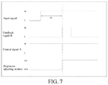
- FIG. 7 is a schematic waveform graph of a display apparatus according to an embodiment of this application.
- a method for driving a display apparatus provides the display apparatus 20 described in the foregoing embodiments.
- the method for driving the display apparatus 20 includes: After the display apparatus 20 is powered on, where the display apparatus 20 may be, for example, turned on, the timing controller 22 reads display data in the storage module 21 , converts the display data to image data for image displaying, and outputs the image data to the display module 24 .
- the display module 24 receives the image data and presents a corresponding displayed image (where in this case, the brightness adjusting module 23 is not lightened, so that there is no light rays to the display module 24 , and the “displayed image” is a working state of each element, for example, a pixel electrode, an active switch, a data line and a scanning line of the display module 24 , instead of an image viewed by a viewer).
- the timing controller 22 finishes configuring an input signal (which may be, for example, a data voltage or a scanning voltage) and reading the display data in the storage module 21 , where a preparation time is T 1 (as shown in FIG.
- the timing controller 22 finishes configuring the image data of the display module 24 , the timing controller 22 receives a feedback signal B sent by the display module 24 , and sends the control signal A to the brightness adjusting module 23 by using the feedback signal B.
- the brightness adjusting module 23 is adjusted from an initial off working state OFF to an on working state ON, and provides a corresponding light source, that is, emits light rays to the display module 24 . In this way, the display apparatus 20 displays a corresponding image for a viewer.
- the method for driving a display apparatus includes the following steps:
- Step S 101 The display apparatus is powered on.
- Step S 102 A timing controller reads display data in a storage module, converts the display data to image data, and outputs the image data and a control signal.
- Step S 103 A display module receives image data, and presents a corresponding image.
- Step S 104 A brightness adjusting module receives the control signal, and adjusts a working state of the brightness adjusting module according to the control signal.
- Step S 105 The timing controller finishes configuring the image data of the display module, and receives a feedback signal sent by the display module.
- Step S 106 The brightness adjusting module is adjusted from an off working state to an on working state.
- the brightness adjusting module 23 receives the control signal A, and the working state of the brightness adjusting module 23 is adjusted according to a potential of the control signal A.
- the potential of the control signal A includes a high potential H and a low potential L, where a high-potential H control signal A may be, for example, a high-potential H square wave signal, a high-potential H triangular wave signal or a high-potential H sine wave signal.
- the brightness adjusting module 23 when the control signal A received by the brightness adjusting module 23 is at the high potential H, the brightness adjusting module 23 is in the on working state.
- the brightness adjusting module 23 when the control signal A received by the brightness adjusting module 23 is at the low potential L, the brightness adjusting module 23 is in the off working state.
- the brightness adjusting module 23 is turned on after preparations of the display module 24 are finished. This can ensure that an abnormal image caused by abnormality of the timing controller 22 is not viewed by a viewer.
- the control signal A may be maintained at a high-potential H all the time.
- the high potential H of the control signal A is transmitted to the brightness adjusting module 23 , causing the brightness adjusting module 23 to be in the ON state.
- the display apparatus 20 of this application includes a display panel.
- the display panel may be equivalent to the display module 24 .
- the display panel may be, for example, a liquid crystal display panel, but is not limited thereto.
- the display panel may alternatively be an OLED display panel, a W-OLED display panel, a QLED display panel, a plasma display panel, a curved surface type display panel, or a display panel of another type.
- the brightness adjusting module 23 is turned on after preparations of the timing controller 22 are finished. This can prevent, when abnormality occurs, an abnormal image from being viewed by a viewer due to that a preparation time of the timing controller 22 is longer than a preset value. In this way, a structure of the display apparatus is optimized and viewer experience is improved.
Landscapes
- Engineering & Computer Science (AREA)
- Physics & Mathematics (AREA)
- Computer Hardware Design (AREA)
- General Physics & Mathematics (AREA)
- Theoretical Computer Science (AREA)
- Chemical & Material Sciences (AREA)
- Crystallography & Structural Chemistry (AREA)
- Control Of Indicators Other Than Cathode Ray Tubes (AREA)
Abstract
Description
Claims (20)
Applications Claiming Priority (4)
| Application Number | Priority Date | Filing Date | Title |
|---|---|---|---|
| CN201810264696.7 | 2018-03-28 | ||
| CN201810264696 | 2018-03-28 | ||
| CN201810264696.7A CN108447452B (en) | 2018-03-28 | 2018-03-28 | Display device and driving method thereof |
| PCT/CN2018/093373 WO2019184115A1 (en) | 2018-03-28 | 2018-06-28 | Display device and driving method therefor |
Publications (2)
| Publication Number | Publication Date |
|---|---|
| US20200013350A1 US20200013350A1 (en) | 2020-01-09 |
| US10825402B2 true US10825402B2 (en) | 2020-11-03 |
Family
ID=63197659
Family Applications (1)
| Application Number | Title | Priority Date | Filing Date |
|---|---|---|---|
| US16/329,158 Active US10825402B2 (en) | 2018-03-28 | 2018-06-28 | Display apparatus and driving method therefor |
Country Status (3)
| Country | Link |
|---|---|
| US (1) | US10825402B2 (en) |
| CN (1) | CN108447452B (en) |
| WO (1) | WO2019184115A1 (en) |
Families Citing this family (4)
| Publication number | Priority date | Publication date | Assignee | Title |
|---|---|---|---|---|
| CN109377957B (en) * | 2018-12-03 | 2020-05-05 | 惠科股份有限公司 | Driving method, driving circuit and display device |
| CN109903713B (en) * | 2019-03-06 | 2020-11-24 | 深圳市华星光电技术有限公司 | Display compensation circuit and display compensation method |
| KR20200130607A (en) * | 2019-05-10 | 2020-11-19 | 삼성디스플레이 주식회사 | Display device and driving method of the same |
| CN111580291B (en) * | 2020-04-24 | 2023-12-22 | 深圳市华星光电半导体显示技术有限公司 | Signal driving plate, production module and production method of display module |
Citations (10)
| Publication number | Priority date | Publication date | Assignee | Title |
|---|---|---|---|---|
| US20080284720A1 (en) * | 2007-05-18 | 2008-11-20 | Semiconductor Energy Laboratory Co., Ltd. | Liquid crystal display device, electronic device, and driving methods thereof |
| CN101389177A (en) | 2007-09-14 | 2009-03-18 | 群康科技(深圳)有限公司 | Light regulating circuit |
| CN101388195A (en) | 2008-08-26 | 2009-03-18 | 矽创电子股份有限公司 | Control chip of color sequential LCD equipment |
| KR20120023233A (en) | 2010-09-01 | 2012-03-13 | 엘지디스플레이 주식회사 | Liquid crystal display device and method for driving the same |
| KR101143602B1 (en) | 2010-01-14 | 2012-05-09 | (주)엠씨테크놀로지 | Liquid crystal display |
| CN102737602A (en) | 2012-06-26 | 2012-10-17 | 青岛海信电器股份有限公司 | Liquid crystal display device and display control method |
| CN102810298A (en) | 2011-06-01 | 2012-12-05 | 仁宝电脑工业股份有限公司 | Method and device for controlling signal-processing of the backlight module of the display device |
| US20140267444A1 (en) * | 2012-10-22 | 2014-09-18 | Shenzen China Star Optoelectronics Technology Co., Ltd. | AMOLED Display Device and Method for Precisely Compensating Aging Thereof |
| US20150187246A1 (en) * | 2013-12-26 | 2015-07-02 | Seiko Epson Corporation | Image display device and control method of image display device |
| US20190064217A1 (en) * | 2017-08-23 | 2019-02-28 | Boe Technology Group Co., Ltd. | Test device and test method |
Family Cites Families (2)
| Publication number | Priority date | Publication date | Assignee | Title |
|---|---|---|---|---|
| CN101989401A (en) * | 2009-07-31 | 2011-03-23 | 晨星软件研发(深圳)有限公司 | Time schedule controller for display device and relevant method thereof |
| CN106205508A (en) * | 2016-09-22 | 2016-12-07 | 昆山龙腾光电有限公司 | Backlight adjusting method and backlight adjusting means for liquid crystal indicator |
-
2018
- 2018-03-28 CN CN201810264696.7A patent/CN108447452B/en active Active
- 2018-06-28 WO PCT/CN2018/093373 patent/WO2019184115A1/en active Application Filing
- 2018-06-28 US US16/329,158 patent/US10825402B2/en active Active
Patent Citations (10)
| Publication number | Priority date | Publication date | Assignee | Title |
|---|---|---|---|---|
| US20080284720A1 (en) * | 2007-05-18 | 2008-11-20 | Semiconductor Energy Laboratory Co., Ltd. | Liquid crystal display device, electronic device, and driving methods thereof |
| CN101389177A (en) | 2007-09-14 | 2009-03-18 | 群康科技(深圳)有限公司 | Light regulating circuit |
| CN101388195A (en) | 2008-08-26 | 2009-03-18 | 矽创电子股份有限公司 | Control chip of color sequential LCD equipment |
| KR101143602B1 (en) | 2010-01-14 | 2012-05-09 | (주)엠씨테크놀로지 | Liquid crystal display |
| KR20120023233A (en) | 2010-09-01 | 2012-03-13 | 엘지디스플레이 주식회사 | Liquid crystal display device and method for driving the same |
| CN102810298A (en) | 2011-06-01 | 2012-12-05 | 仁宝电脑工业股份有限公司 | Method and device for controlling signal-processing of the backlight module of the display device |
| CN102737602A (en) | 2012-06-26 | 2012-10-17 | 青岛海信电器股份有限公司 | Liquid crystal display device and display control method |
| US20140267444A1 (en) * | 2012-10-22 | 2014-09-18 | Shenzen China Star Optoelectronics Technology Co., Ltd. | AMOLED Display Device and Method for Precisely Compensating Aging Thereof |
| US20150187246A1 (en) * | 2013-12-26 | 2015-07-02 | Seiko Epson Corporation | Image display device and control method of image display device |
| US20190064217A1 (en) * | 2017-08-23 | 2019-02-28 | Boe Technology Group Co., Ltd. | Test device and test method |
Also Published As
| Publication number | Publication date |
|---|---|
| WO2019184115A1 (en) | 2019-10-03 |
| CN108447452B (en) | 2020-03-27 |
| US20200013350A1 (en) | 2020-01-09 |
| CN108447452A (en) | 2018-08-24 |
Similar Documents
| Publication | Publication Date | Title |
|---|---|---|
| US10825402B2 (en) | Display apparatus and driving method therefor | |
| KR20190137658A (en) | Display panel | |
| US8982030B2 (en) | Gate output control method and corresponding gate pulse modulator | |
| KR20190136882A (en) | Display panel and driving method of the display panel | |
| CN109523957B (en) | Drive circuit, backlight module and display panel | |
| US10446100B2 (en) | Array substrate, liquid crystal display and display device | |
| US9548723B1 (en) | Current mode DVR or PVCOM with integrated impedances | |
| KR102487518B1 (en) | Data driving circuit and display apparatus having the same | |
| JP2008191535A (en) | Display device | |
| JP4905635B2 (en) | Display drive device | |
| EP3174040B1 (en) | Display device and driving method thereof | |
| JP4916244B2 (en) | Liquid crystal display | |
| US11468862B2 (en) | Drive circuit and method for display apparatus | |
| US10962845B1 (en) | Driving system of display device, driving method and display device | |
| TWI440002B (en) | Driving circuit of liquid crystal panel and liquid crystal device | |
| US20180322839A1 (en) | Display panel and display apparatus using same | |
| WO2016165164A1 (en) | Multi-voltage generation apparatus and liquid crystal display | |
| US8395603B2 (en) | Electronic device including display device and driving method thereof | |
| KR20220089230A (en) | Display Device Including Data Driving Part | |
| KR101610371B1 (en) | Driver IC for liquid crystal display apparatus | |
| US10037740B2 (en) | GOA circuit and liquid crystal display device | |
| KR101216172B1 (en) | Liquid crystal display | |
| CN113053327B (en) | Display driving device, display driving method and display equipment | |
| US20120229441A1 (en) | Liquid crystal display panel | |
| KR102340939B1 (en) | Display device and driving method thereof |
Legal Events
| Date | Code | Title | Description |
|---|---|---|---|
| FEPP | Fee payment procedure |
Free format text: ENTITY STATUS SET TO UNDISCOUNTED (ORIGINAL EVENT CODE: BIG.); ENTITY STATUS OF PATENT OWNER: LARGE ENTITY |
|
| AS | Assignment |
Owner name: HKC CORPORATION LIMITED, CHINA Free format text: ASSIGNMENT OF ASSIGNORS INTEREST;ASSIGNOR:HUANG, XIAOYU;REEL/FRAME:048469/0938 Effective date: 20180712 Owner name: CHONGQING HKC OPTOELECTRONICS TECHNOLOGY CO., LTD. Free format text: ASSIGNMENT OF ASSIGNORS INTEREST;ASSIGNOR:HUANG, XIAOYU;REEL/FRAME:048469/0938 Effective date: 20180712 Owner name: CHONGQING HKC OPTOELECTRONICS TECHNOLOGY CO., LTD., CHINA Free format text: ASSIGNMENT OF ASSIGNORS INTEREST;ASSIGNOR:HUANG, XIAOYU;REEL/FRAME:048469/0938 Effective date: 20180712 |
|
| STPP | Information on status: patent application and granting procedure in general |
Free format text: DOCKETED NEW CASE - READY FOR EXAMINATION |
|
| STPP | Information on status: patent application and granting procedure in general |
Free format text: NON FINAL ACTION MAILED |
|
| STPP | Information on status: patent application and granting procedure in general |
Free format text: RESPONSE TO NON-FINAL OFFICE ACTION ENTERED AND FORWARDED TO EXAMINER |
|
| STPP | Information on status: patent application and granting procedure in general |
Free format text: NOTICE OF ALLOWANCE MAILED -- APPLICATION RECEIVED IN OFFICE OF PUBLICATIONS |
|
| STPP | Information on status: patent application and granting procedure in general |
Free format text: PUBLICATIONS -- ISSUE FEE PAYMENT VERIFIED |
|
| STCF | Information on status: patent grant |
Free format text: PATENTED CASE |
|
| MAFP | Maintenance fee payment |
Free format text: PAYMENT OF MAINTENANCE FEE, 4TH YEAR, LARGE ENTITY (ORIGINAL EVENT CODE: M1551); ENTITY STATUS OF PATENT OWNER: LARGE ENTITY Year of fee payment: 4 |