CN101271870B - Silicon epitaxial wafer - Google Patents
Silicon epitaxial wafer Download PDFInfo
- Publication number
- CN101271870B CN101271870B CN2008100955430A CN200810095543A CN101271870B CN 101271870 B CN101271870 B CN 101271870B CN 2008100955430 A CN2008100955430 A CN 2008100955430A CN 200810095543 A CN200810095543 A CN 200810095543A CN 101271870 B CN101271870 B CN 101271870B
- Authority
- CN
- China
- Prior art keywords
- silicon substrate
- monocrystalline silicon
- silicon
- vapor phase
- peripheral part
- Prior art date
- Legal status (The legal status is an assumption and is not a legal conclusion. Google has not performed a legal analysis and makes no representation as to the accuracy of the status listed.)
- Active
Links
Images


Classifications
-
- E—FIXED CONSTRUCTIONS
- E04—BUILDING
- E04D—ROOF COVERINGS; SKY-LIGHTS; GUTTERS; ROOF-WORKING TOOLS
- E04D11/00—Roof covering, as far as not restricted to features covered by only one of groups E04D1/00 - E04D9/00; Roof covering in ways not provided for by groups E04D1/00 - E04D9/00, e.g. built-up roofs, elevated load-supporting roof coverings
- E04D11/02—Build-up roofs, i.e. consisting of two or more layers bonded together in situ, at least one of the layers being of watertight composition
-
- E—FIXED CONSTRUCTIONS
- E04—BUILDING
- E04D—ROOF COVERINGS; SKY-LIGHTS; GUTTERS; ROOF-WORKING TOOLS
- E04D13/00—Special arrangements or devices in connection with roof coverings; Protection against birds; Roof drainage; Sky-lights
- E04D13/17—Ventilation of roof coverings not otherwise provided for
Landscapes
- Engineering & Computer Science (AREA)
- Architecture (AREA)
- Civil Engineering (AREA)
- Structural Engineering (AREA)
- Weting (AREA)
- Chemical Vapour Deposition (AREA)
- Crystals, And After-Treatments Of Crystals (AREA)
Abstract
The invention provides a silicon extension sheet, which has monocrystal line silicon uropatagia. The silicon extension sheet is formed on the silicon filam on the back of the monocrystal line silicon uropatagia, and formed on silicon extension layer of the main surface of the monocrystal line silicon uropatagia, characterized in that the periphery filam which extents from the back of the monocrystal line silicon uropatagia to at least the outer edge of the periphery of the monocrystal line silicon uropatagia onle exists on part of the periphery potion.
Description
The application is to be that May 21, application number in 2004 are dividing an application of 200410045706.6 Chinese invention patent application the applying date.
Technical field
The present invention relates to the surface treatment method of monocrystalline silicon substrate, the manufacture method and the silicon epitaxial wafer of silicon epitaxial wafer.
Background technology
In the past, as the device of vapor phase growth silicon epitaxy layer on the first type surface of monocrystalline silicon substrate, what for example use is the cylinder type epitaxially growing equipment.This epitaxially growing equipment has the pedestal that is polygonal pyramid platform shape in the inside of reacting furnace.On the outer peripheral face of pedestal, be formed with spot-facing portion, when carrying out vapor phase growth monocrystalline silicon substrate be upright state and be positioned over wherein.
But, when adopting the silicon epitaxy layer of this epitaxially growing equipment vapor phase growth high resistivity on the first type surface of the monocrystalline silicon substrate of low-resistivity, dopant in the monocrystalline silicon substrate takes place easily from once be discharged into the phenomenon that is doped to the gas phase in the silicon epitaxy layer, i.e. auto-doping phenomenon such as the back side of monocrystalline silicon substrate etc.For this reason, before carrying out vapor phase growth, form the silicon oxide layer that anti-autodoping is used at the back side of monocrystalline silicon substrate.
Yet, when adopting the CVD method to form above-mentioned silicon oxide layer, silicon oxide layer is that first type surface one side that the back side from monocrystalline silicon substrate is extended to peripheral part forms, therefore, during vapor phase growth on the main surface side of the peripheral part of monocrystalline silicon substrate, can produce dough 5 as shown in Figure 9, i.e. Kuai Zhuan polysilicon.And this dough 5 can cause coming off and producing particle from silicon epitaxial wafer.For this reason, as the method that prevents to produce above-mentioned dough, the past attempts proposition is carried out vapor phase growth under the removed state of silicon oxide layer of the whole peripheral part of monocrystalline silicon substrate method (for example can open flat 1-248527 communique) with reference to the spy.
But, adopt above-mentioned spy to open the disclosed method of flat 1-248527 communique, during with the thicker silicon epitaxy layer of for example cylinder type epitaxially growing equipment vapor phase growth on the first type surface of monocrystalline silicon substrate, this phenomenon takes place sometimes, promptly, this silicon epitaxy layer of the two sandwich of said base and monocrystalline silicon substrate sticks together, and cracks on silicon epitaxial wafer.For this reason, as the method that prevents to produce above-mentioned crackle, once proposed under the state that the speed of growth of silicon epitaxy layer is controlled, to carry out the method (for example can open flat 8-279470 communique) of vapor phase growth with reference to the spy.
And adopt above-mentioned spy to open the method for flat 8-279470 communique, though can prevent the generation of crackle, because the speed of growth of silicon epitaxy layer is lower, the productivity ratio of silicon epitaxial wafer will reduce significantly.
Summary of the invention
Task of the present invention is, provide a kind of under the state that the generation of auto-doping phenomenon, particle and crackle is suppressed, while can keep the surface treatment method of higher speed of growth vapor phase growth silicon epitaxy layer on the first type surface of monocrystalline silicon substrate, the manufacture method and the silicon epitaxial wafer of silicon epitaxial wafer.
According to an aspect of of the present present invention, a kind of silicon epitaxial wafer is provided, has monocrystalline silicon substrate, be formed at the silicon oxide layer at the back side of this monocrystalline silicon substrate, and be formed at silicon epitaxy layer on the first type surface of above-mentioned monocrystalline silicon substrate, it is characterized in that, be extended to the periphery oxide-film of outer most edge at least of the peripheral part of this monocrystalline silicon substrate from the above-mentioned back side of above-mentioned monocrystalline silicon substrate, exist only on the part of above-mentioned peripheral part.
According to silicon epitaxial wafer of the present invention, its feature is that also above-mentioned periphery oxide-film is formed at the zone below 1/4 of the peripheral part of above-mentioned monocrystalline silicon substrate.
According to the present invention, by monocrystalline silicon substrate is immersed in the hydrofluoric acid (aqueous hydrogen fluoride solution) with the covered state of the silicon oxide layer at the monocrystalline silicon substrate back side, the silicon oxide layer at the monocrystalline silicon substrate back side is not corroded and remains, therefore, generation that can the inhibition of self-doped phenomenon when carrying out vapor phase growth.
Why produce dough this moment, be because the silicon oxide layer of the peripheral part of the monocrystalline silicon substrate that under the state of uneven thickness, forms than unfertile land, when vapor phase growth, corroded and cause the monocrystalline silicon substrate locality to expose, and silicon is in the cause of this exsertion part vapor phase growth by hydrogen.For this reason, by monocrystalline silicon substrate is immersed in the hydrofluoric acid with the state that the part of the peripheral part of monocrystalline silicon substrate is exposed on the liquid level, can make the part beyond the residual periphery oxide-film in the hydrofluoric acid treatment operation among the peripheral part of monocrystalline silicon substrate, be in the state that is not covered, can prevent the generation of dough by silicon oxide layer.In addition, even if residual periphery oxide-film in the hydrofluoric acid treatment operation, it is easy to generate the part of dough, it is silicon oxide layer thinner thickness among the territory, first type surface one lateral areas of monocrystalline silicon substrate peripheral part, corrode the part that sparsely to be removed through hydrogen, can be evaporated hydrofluoric acid vapor from hydrofluoric acid corrodes in advance and removes, and thicker silicon oxide layer left behind, therefore, when carrying out vapor phase growth, can prolong the residual silicon oxide-film is corroded by hydrogen and causes the monocrystalline silicon substrate part to expose the needed time, correspondingly, can make the generation of dough become difficult.Its result can suppress the generation of the particle that caused by dough.
And why can on silicon epitaxial wafer, crack, be since be deposited in polysilicon layer and vapor phase growth on the monocrystalline silicon substrate first type surface on the base-plates surface silicon epitaxy layer the two, near pedestal and the contacted position of monocrystalline silicon substrate, become one, and when cooling off, produce the cause of thermal stress in this part., contact with pedestal for this reason, can make between the peripheral part of monocrystalline silicon substrate and the pedestal to be in contactless state by making the residual periphery oxide-film of a part.In addition, because can the vapor phase growth silicon epitaxy layer on the silicon oxide layer, therefore, under this state, carry out vapor phase growth, the silicon epitaxy layer that is deposited in polysilicon layer and vapor phase growth on the monocrystalline silicon substrate first type surface on the base-plates surface can not become one, therefore, after vapor phase growth finishes, can suppress the generation of crackle on the silicon epitaxial wafer.
According to above way, even do not reduce the speed of growth of silicon epitaxy layer, also under the state that can be suppressed in the generation of auto-doping phenomenon, particle and crackle, vapor phase growth silicon epitaxy layer on through the first type surface of the monocrystalline silicon substrate after the above-mentioned surface treatment.
In addition, according to the 2nd aspect of the present invention, as the surface treatment method of monocrystalline silicon substrate of the present invention, be to form operation and make the order of the hydrofluoric acid treatment operation that hydrofluoric acid vapor contacts with the peripheral part of first type surface one side of monocrystalline silicon substrate carry out above-mentioned operation according to the oxide-film that forms silicon oxide layer with chemical vapor deposition (CVD) method at the back side of monocrystalline silicon substrate.
According to the present invention, by forming silicon oxide layer at the back side of monocrystalline silicon substrate, can make the back side of monocrystalline silicon substrate be in the state that covers by silicon oxide layer with the CVD method, therefore, generation that can the inhibition of self-doped phenomenon when carrying out vapor phase growth.
In addition, by hydrofluoric acid vapor is contacted with the peripheral part of first type surface one side of monocrystalline silicon substrate, can the part of dough will be easy to generate among the formed silicon oxide layer on first type surface one side of monocrystalline silicon substrate peripheral part, the part that is the silicon oxide layer thinner thickness, can be sparsely removed through hydrogen corrosion, erode in advance, and thicker silicon oxide layer be left behind.Therefore, when carrying out vapor phase growth, can prolong residual silicon oxide layer and be corroded by hydrogen and cause the monocrystalline silicon substrate part to expose the needed time, correspondingly, can make the generation of the dough difficulty that becomes.Its result can suppress the generation of the particle that caused by dough.
In addition, when being placed into monocrystalline silicon substrate on the pedestal, contact with pedestal, can make between the peripheral part of monocrystalline silicon substrate and the pedestal to be in contactless state by making the silicon oxide layer on the peripheral part that remains in monocrystalline silicon substrate.In addition, because can the vapor phase growth silicon epitaxy layer on the silicon oxide layer, therefore, under this state, carry out vapor phase growth, the silicon epitaxy layer that is deposited in polysilicon layer and vapor phase growth on the first type surface of monocrystalline silicon substrate on the base-plates surface can not become one, therefore, after vapor phase growth finishes, can suppress the generation of crackle on the silicon epitaxial wafer.
According to above way, even do not reduce the speed of growth of silicon epitaxy layer, also under the state that can be suppressed in the generation of auto-doping phenomenon, particle and crackle, vapor phase growth silicon epitaxy layer on through the first type surface of the monocrystalline silicon substrate after the above-mentioned surface treatment.
In addition, according to the 3rd aspect of the present invention,, carry out in order forming operation at the oxide-film that the back side of monocrystalline silicon substrate forms silicon oxide layer with the CVD method as the manufacture method of silicon epitaxial wafer of the present invention; Be immersed in the hydrofluoric acid by monocrystalline silicon substrate is formed at the state that the part of the peripheral part of the silicon oxide layer at the monocrystalline silicon substrate back side and monocrystalline silicon substrate is exposed on the liquid level with covering, make the periphery oxide-film that is extended to the outer most edge at least of peripheral part from the back side of monocrystalline silicon substrate only residue in the hydrofluoric acid treatment operation on the part of peripheral part; And in making the hydrofluoric acid treatment operation under the state of the contacts side surfaces of the spot-facing portion of residual periphery oxide-film and pedestal, the vapor phase growth operation of vapor phase growth silicon epitaxy layer on the first type surface of monocrystalline silicon substrate.
With the zone 1/4 below of the peripheral part of monocrystalline silicon substrate be exposed to state liquid level on preferably in the hydrofluoric acid treatment operation this moment, and monocrystalline silicon substrate is immersed in the hydrofluoric acid.
According to the present invention, by monocrystalline silicon substrate is immersed in the hydrofluoric acid by the state that the CVD method is formed at the silicon oxide layer at the monocrystalline silicon substrate back side with covering, the silicon oxide layer at the monocrystalline silicon substrate back side is not corroded and remains, therefore, generation that can the inhibition of self-doped phenomenon when carrying out the vapor phase growth operation.
In addition, adopt the CVD method on the territory, first type surface one lateral areas of the peripheral part that centers on monocrystalline silicon substrate, also can form silicon oxide layer, but by with monocrystalline silicon substrate with the part of the peripheral part of monocrystalline silicon substrate, preferably 1/4 state that is exposed on the liquid level with lower area of peripheral part is immersed in the hydrofluoric acid, can make the part beyond the residual periphery oxide-film in the hydrofluoric acid treatment operation among the peripheral part of monocrystalline silicon substrate, be in the state that is not covered, thereby prevent the generation of dough by silicon oxide layer.And, even if the residual periphery oxide-film of part in the hydrofluoric acid treatment operation, when particularly being exposed on the hydrofluoric acid liquid level in the zone below 1/4 of peripheral part, whole periphery oxide-film residual in the hydrofluoric acid treatment operation contacts with hydrofluoric acid vapor, it is easy to generate the part of dough, it is silicon oxide layer thinner thickness among the territory, first type surface one lateral areas of monocrystalline silicon substrate peripheral part, and the part that can sparsely be removed through hydrogen corrosion, the hydrofluoric acid vapor that can be evaporated from hydrofluoric acid erodes in advance, and thicker silicon oxide layer left behind.Therefore, when carrying out the vapor phase growth operation, can prolong residual silicon oxide layer and be corroded by hydrogen and cause the monocrystalline silicon substrate part to expose the needed time, correspondingly, can make the territory, first type surface one lateral areas of the peripheral part of monocrystalline silicon substrate be difficult to produce dough.Its result can suppress the generation of the particle that caused by dough.
When the vapor phase growth silicon epitaxy layer, contact with pedestal by making periphery oxide-film residual in the hydrofluoric acid treatment operation, can make to be in contactless state between the peripheral part of monocrystalline silicon substrate and the pedestal.In addition, because can the vapor phase growth silicon epitaxy layer on the silicon oxide layer, therefore, under this state, carry out the vapor phase growth operation, the silicon epitaxy layer that is deposited in polysilicon layer and vapor phase growth on the first type surface of monocrystalline silicon substrate on the base-plates surface can not become one, therefore, can suppress the generation of crackle on the silicon epitaxial wafer.
According to above way, even do not reduce the speed of growth of silicon epitaxy layer, also under the state that can be suppressed in the generation of auto-doping phenomenon, particle and crackle, vapor phase growth silicon epitaxy layer on the first type surface of monocrystalline silicon substrate.
According to the present invention, be the state that is formed with silicon oxide layer at the back side of monocrystalline silicon substrate, promptly under the state that is suppressed of auto-doping phenomenon, on the first type surface of monocrystalline silicon substrate, form silicon epitaxy layer.Therefore, when on the first type surface of monocrystalline silicon substrate, forming silicon epitaxy layer, be under the back side of monocrystalline silicon substrate is formed with the state of silicon oxide layer, to carry out vapor phase growth, thereby can be under the situation about being suppressed of auto-doping phenomenon the vapor phase growth silicon epitaxy layer.
In addition, owing to be extended to the periphery oxide-film of outer most edge at least of the peripheral part of this monocrystalline silicon substrate from the back side of monocrystalline silicon substrate, exist only in the part of above-mentioned peripheral part, the zone below 1/4 of peripheral part preferably, therefore, when on the first type surface of monocrystalline silicon substrate, forming silicon epitaxy layer, by the periphery oxide-film is contacted with pedestal, can be at the peripheral part of monocrystalline silicon substrate and pedestal and carry out vapor phase growth under the non-contacting state.In addition, because can the vapor phase growth silicon epitaxy layer on the silicon oxide layer, therefore, the silicon epitaxy layer that is deposited in polysilicon layer and vapor phase growth on the first type surface of monocrystalline silicon substrate on the base-plates surface can not become one, therefore, can suppress the generation of crackle on the silicon epitaxial wafer.In addition, the part beyond the periphery oxide-film among the peripheral part of monocrystalline silicon substrate is in the state that is not covered by silicon oxide layer, i.e. can not produce the state of dough during vapor phase growth.Therefore, when on the first type surface of monocrystalline silicon substrate, forming silicon epitaxy layer, be under the state that the part in addition of the periphery oxide-film among the peripheral part of monocrystalline silicon substrate is not covered by silicon oxide layer, to carry out vapor phase growth, therefore, vapor phase growth silicon epitaxy layer under the situation that can be suppressed in the generation of the particle that causes by dough.
According to above way, can access a kind of like this silicon epitaxial wafer, promptly, even do not reduce the speed of growth of silicon epitaxy layer, also can be under the state that the auto-doping phenomenon that produces on the first type surface of monocrystalline silicon substrate, particle and crackle are suppressed, vapor phase growth silicon epitaxy layer on the first type surface of monocrystalline silicon substrate.
Description of drawings
Can fully understand the present invention by following detailed description and accompanying drawing, but this only is in order to describe, and is not that scope of the present invention is limited.
Figure 1A, 1B are the figure of expression silicon epitaxial wafer involved in the present invention, and Figure 1A is a longitudinal sectional view, and Figure 1B is the vertical view of first type surface one side.
Fig. 2 A~2C is to be used for the figure that manufacture method to silicon epitaxial wafer involved in the present invention describes.
Fig. 3 is the longitudinal sectional view of hydrofluoric acid treatment apparatus.
Fig. 4 is the longitudinal sectional view of the general configuration of expression epitaxially growing equipment.
Fig. 5 A, 5B are the vertical view and the longitudinal sectional views of other form of implementation of expression silicon epitaxial wafer involved in the present invention.
Fig. 6 is the longitudinal sectional view of hydrofluoric acid treatment apparatus.
Fig. 7 is the figure that concerns between expression cracking frequency and the vapor phase growth speed.
Fig. 8 is the figure that concerns between the expression generation number of particle and vapor phase growth speed and the periphery oxide-film residual quantity.
Fig. 9 is the longitudinal sectional view that is formed with the silicon epitaxial wafer of dough.
Embodiment
Below, to form of implementation of the present invention in conjunction with the accompanying drawings.
<the 1 form of implementation 〉
At first, the form of implementation to silicon epitaxial wafer involved in the present invention describes.
Figure 1A, 1B are the figure of expression silicon epitaxial wafer 1.As shown in the drawing, silicon epitaxial wafer 1 has the monocrystalline silicon substrate 10 that approximately is the disk shape.Shown in Figure 1B, be formed with location flat part (below be called flat part) 11 on the monocrystalline silicon substrate 10.On the first type surface 12 of monocrystalline silicon substrate 10, be formed with silicon epitaxy layer 13, be formed with silicon oxide layer 15 at the back side 14 of monocrystalline silicon substrate 10.Silicon oxide layer 15 has periphery oxide-film 110 among the peripheral part 16 of monocrystalline silicon substrate 10 and parts flat part 11 opposite sides.This periphery oxide-film 110 forms on the zone below 1/4 of peripheral part 16, is to form on 1/8 zone in this form of implementation, is central angle and is 45 ° circular-arc.And the X of outer most edge at least that is extended to the peripheral part 16 of this monocrystalline silicon substrate 10 from the back side 14 of monocrystalline silicon substrate 10 forms this periphery oxide-film 110.
Below, the manufacture method of silicon epitaxial wafer involved in the present invention 1 is described.
When making silicon epitaxial wafer 1, at first, the monocrystal silicon to for example making with methods such as FZ method or CZ methods carries out slicing process, chamfering process, grinding step and corrosion process in order, generates the monocrystalline silicon substrate 10 shown in Fig. 2 A.
Secondly, form silicon oxide layer 15 at the back side 14 of monocrystalline silicon substrate 10, generate the substrate 17 (oxide-film formation operation) shown in Fig. 2 B with methods such as normal CVD methods.Specifically, in that monocrystalline silicon substrate 10 is heated in 350~450 ℃, unstrpped gas is blown on its back side 14 with vector gas.Thus, on the back side 14 of monocrystalline silicon substrate 10, form silicon oxide layer 15.And this silicon oxide layer 15 also forms on the territory, first type surface 12 1 lateral areas among the peripheral part 16 of monocrystalline silicon substrate 10, becomes periphery oxide-film 110.As unstrpped gas, preferably use silane (SiH
4) mist of gas and oxygen, as vector gas, preferably use inert gases such as nitrogen.
Secondly, the peripheral part 16 of substrate 17 is implemented hydrofluoric acid (HF) handle, generate the substrate 18 (hydrofluoric acid treatment operation) shown in Fig. 2 C.Substrate 18, overleaf 14 and the zone below 1/4 of peripheral part 16 (among Fig. 2 left side peripheral part 16), be to have periphery oxide-film 110 on 1/8 the zone in this form of implementation, but the zone at other peripheral part 16 (peripheral part 16 on right side among Fig. 2) does not have periphery oxide-film 110.The central angle of periphery oxide-film 110 formed circular arcs is 45 °.And the central angle of above-mentioned circular arc, preferably more than 3 °.
In this hydrofluoric acid treatment operation, for example can use hydrofluoric acid treatment apparatus shown in Figure 32.Hydrofluoric acid treatment apparatus 2 is full of in the bath 20 of diluted hydrofluoric acid (aqueous hydrogen fluoride solution) F in inside, has the clamping device 21 that a plurality of substrates 17 are carried out clamping.Clamping device 21 can be to carrying out clamping by be corrosion-resistant plate 22 and the substrate 17 alternately laminated duplexers that form 23 that the shape identical substantially with substrate 17 form with materials such as vinyl chloride.More particularly, clamping device 21 under the state that the flat part 11 of the monocrystalline silicon substrate 10 of substrate 17 aligns down, carries out clamping and they is closely contacted each other with corrosion-resistant plate 22 substrate 17.As this hydrofluoric acid treatment apparatus 2, for example there is the spy to open the disclosed device of flat 1-248527 communique.On the top of bath 20, have hydrofluoric acid vapor V by diluted hydrofluoric acid F evaporation.
State in the use in the hydrofluoric acid treatment operation of hydrofluoric acid treatment apparatus 2, at first,, duplexer 23 is immersed among the diluted hydrofluoric acid F in the bath 20 with flat part 11 state down of substrate 17 with clamping device 21 clamping duplexers 23.At this moment, make the upper end of duplexer 23, the part with peripheral parts 16 flat part 11 opposite sides promptly substrate 17 is exposed on the liquid level of diluted hydrofluoric acid F.The central angle of the formed circular arc of a part of peripheral part 16 that is exposed to the substrate 17 on the liquid level is preferably in (below 1/4 of peripheral part 16) more than 3 °, below 90 °.In this case, the part of the peripheral part 16 of substrate 17 is exposed on the diluted hydrofluoric acid F and is exposed among the hydrofluoric acid vapor V.
So, on among the territory, first type surface 12 1 lateral areas of the peripheral part 16 of substrate 17 and parts flat part 11 opposite sides, will be shown in the left side peripheral part 16 of Fig. 2 C residual periphery oxide-film 110, and the part beyond this periphery oxide-film 110, to shown in the right side peripheral part 16 of Fig. 2 C, be in the state that no silicon oxide layer covers.More particularly, even if periphery oxide-film 110, it is easy to generate the part of dough, the part that is the thinner thickness of periphery oxide-film 110, in vapor phase growth operation described later, can be sparsely removed through the hydrogen corrosion, can be eroded by hydrofluoric acid vapor V, and thicker silicon oxide layer left behind by diluted hydrofluoric acid F evaporation.,, thereby have the zone that is not exposed among the hydrofluoric acid vapor V here, then should be easy to generate dough 5 on the peripheral part 16 in zone if the central angle of peripheral part 16 formed circular arcs that is exposed to the substrate 17 on the liquid level of diluted hydrofluoric acid F is greater than 90 °.
In addition, the silicon oxide layer 15 at the back side 14 of substrate 17 can not be corroded and remain.
Secondly, the substrate 18 that is generated is carried out mirror ultrafinish and cleaning.
Then, form silicon epitaxy layer 13 (vapor phase growth operation) on the top of the first type surface 12 of substrate 18.
In this vapor phase growth operation, for example can use cylinder type epitaxially growing equipment 3 shown in Figure 4.This epitaxially growing equipment 3 has the reacting furnace 30 that a plurality of substrates 18 can be placed in inside.The sidewall 30a of reacting furnace 30 forms by light transmission is quartzy, is formed with air supply opening 30b on this sidewall 30a.On the diapire 30c of reacting furnace 30, be formed with exhaust outlet 30d.In the side of reacting furnace 30, dispose a plurality of heaters 31 that carry out radiation through sidewall 30a to reacting furnace 30 inside.In the inside of reacting furnace 30, dispose the pedestal 32 that is polygonal pyramid platform shape of the state configuration of suspending in midair with roof 30e from reacting furnace 30.This pedestal 32 can rotate under the driving of rotating driving device (not shown), on its each outer peripheral face 32a, is formed with for example a plurality of spot-facing such as epimere, stage casing, hypomere portion 33.In each spot-facing portion 33, can be upright state and place substrate 18.
State in the use in the vapor phase growth operation of epitaxially growing equipment 3, at first, substrate 18 is placed in each spot-facing portion 33 of pedestal 32.At this moment, make periphery oxide-film 110 be positioned at the below, with the contacts side surfaces of the spot-facing portion 33 of pedestal 32.So, because periphery oxide-film 110 is between the side of the peripheral part 16 of the monocrystalline silicon substrate 10 of substrate 18 and spot-facing portion 33, thereby the side of peripheral part 16 and spot-facing portion 33 is in contactless state.And, when the central angle of periphery oxide-film 110 formed circular arcs more than 3 ° the time, can make periphery oxide-film 110 really between the side of peripheral part 16 and spot-facing portion 33.Secondly, substrate 18 is being heated in 1100~1200 ℃, is driving pedestal 32 rotations with above-mentioned rotating driving device with heater 31.And, under this state, by with trichlorosilane (SiHCl
3) reacting gas such as gas supplies with in reacting furnace 30 with vector gas such as hydrogen, makes silicon epitaxy layer 13 vapor phase growths.Carry out the vapor phase growth operation under the non-contacting state by being in the side of the peripheral part 16 of substrate 18 and spot-facing portion 33 as mentioned above, can make the silicon epitaxy layer 13 of vapor phase growth on the first type surface 12 of the lip-deep polysilicon layer that is deposited in pedestal 32 and substrate 18 be in the state that can not become one.In addition, though this moment, periphery oxide-film 110 was subjected to the corrosion of hydrogen because periphery oxide-film 110 is to be made of thicker silicon oxide layer, even thereby be corroded, also be not easy to make monocrystalline silicon substrate 10 to expose.
According to the manufacture method of aforesaid silicon epitaxial wafer 1, can make the silicon oxide layer 15 at the back side 14 of monocrystalline silicon substrate 10 not be corroded and remain, therefore, generation that can the inhibition of self-doped phenomenon when carrying out the vapor phase growth operation.
In addition, can make the part beyond the periphery oxide-film 110 residual in the hydrofluoric acid treatment operation among the peripheral part 16 of monocrystalline silicon substrate 10, be in the state that is not covered by silicon oxide layer, and, even if residual periphery oxide-film 110 in the hydrofluoric acid treatment operation, it is easy to generate the part of dough, it is the part of silicon oxide layer thinner thickness among the territory, first type surface 12 1 lateral areas of peripheral part 16, can be eroded in advance by hydrofluoric acid vapor V, and thicker silicon oxide layer left behind by diluted hydrofluoric acid F evaporation.Therefore, when carrying out the vapor phase growth operation, can prolong residual silicon oxide layer is corroded by hydrogen and causes the monocrystalline silicon substrate part to expose the needed time, correspondingly, make the generation of dough become difficult, therefore, can suppress dough comes off and the phenomenon that becomes particle takes place from silicon epitaxial wafer 1.
In addition, even do not reduce the speed of growth of silicon epitaxy layer, in the vapor phase growth operation, the silicon epitaxy layer 13 that is deposited in vapor phase growth on the first type surface 12 of pedestal 32 lip-deep polysilicon layers and monocrystalline silicon substrate 10 can not become one yet.
According to above way, can accomplish that keep higher vapor phase growth speed, under the state that the generation of auto-doping phenomenon, particle and crackle is suppressed, vapor phase growth goes out silicon epitaxy layer 13 on the first type surface 12 of monocrystalline silicon substrate 10.
<the 2 form of implementation 〉
Below, the 2nd form of implementation of the present invention is described.The same inscape of all and above-mentioned the 1st form of implementation is given identical numbering, and its explanation is omitted.
Silicon epitaxial wafer 1A in this 2nd form of implementation is formed with silicon oxide layer 15A at the back side 14 of monocrystalline silicon substrate 10 shown in Fig. 5 A, 5B.Silicon oxide layer 15A has periphery oxide-film 110A on the complete cycle of the peripheral part 16 of monocrystalline silicon substrate 10; The X of outer most edge at least that is extended to the peripheral part 16 of this monocrystalline silicon substrate 10 at the back side 14 from monocrystalline silicon substrate 10 forms this periphery oxide-film 110A.
Below, the manufacture method of silicon epitaxial wafer 1A involved in the present invention is described.The manufacture method of silicon epitaxial wafer 1A in this 2nd form of implementation, have with above-mentioned the 1st form of implementation in the different hydrofluoric acid treatment operation of hydrofluoric acid treatment operation.Below, be elaborated with regard to this point.
Hydrofluoric acid treatment operation in this 2nd form of implementation is exposed among the hydrofluoric acid vapor V first type surface 12 1 sides of the substrate 17 that is formed with silicon oxide layer 15A on the back side 14 and carries out.
More particularly, the hydrofluoric acid treatment operation can utilize hydrofluoric acid treatment apparatus 2A for example shown in Figure 6 to carry out.Hydrofluoric acid treatment apparatus 2A has the bath 20 that inside is full of diluted hydrofluoric acid F.Have the hydrofluoric acid vapor V that evaporates by diluted hydrofluoric acid F on the top of bath 20.
In using the hydrofluoric acid treatment operation of this hydrofluoric acid treatment apparatus 2A, the state that substrate 17 is arranged in the below with first type surface 12 is placed on the hydrofluoric acid vapor V on the top of hydrofluoric acid treatment apparatus 2A.Thus, the first type surface 12 of substrate 17 is exposed among the hydrofluoric acid vapor V, the part of silicon oxide layer thinner thickness among the silicon oxide layer 15A of first type surface 12 1 sides on the peripheral part 16 of substrate 17, the part that promptly is easy to generate dough is corroded.And the silicon oxide layer 15A at the back side 14 of monocrystalline silicon substrate 10 can not be corroded and remain.
According to the manufacture method of aforesaid silicon epitaxial wafer 1A, can make the back side of monocrystalline silicon substrate 10 be in the state that is covered by silicon oxide layer 15A, therefore, generation that can the inhibition of self-doped phenomenon when carrying out vapor phase growth.
And, the partial corrosion that is easy to generate dough among the silicon oxide layer of first type surface 12 1 sides on the peripheral part 16 of monocrystalline silicon substrate 10 can be fallen, and the thicker silicon oxide layer of thickness be left behind.So, when carrying out vapor phase growth, can prolong the residual silicon oxide-film and be corroded by hydrogen and cause monocrystalline silicon substrate 10 parts to expose the needed time, correspondingly, the generation of the dough difficulty that becomes can be made, therefore, the generation of the particle that causes by dough can be suppressed.
In addition, when carrying out the vapor phase growth operation, on the complete cycle of the peripheral part 16 by making monocrystalline silicon substrate 10 the contacts side surfaces of spot-facing portion 33 of residual periphery oxide-film 110A and pedestal 32, can make periphery oxide-film 110A really between the side of the peripheral part 16 of monocrystalline silicon substrate 10 and spot-facing portion 33, thereby can make the peripheral part 16 and the side of spot-facing portion 33 be in contactless state.Therefore, carry out vapor phase growth under this state, the silicon epitaxy layer 13 that is deposited in vapor phase growth on the first type surface 12 of pedestal 32 lip-deep polysilicon layers and monocrystalline silicon substrate 10 can not become one, and therefore, can suppress the generation that silicon epitaxial wafer 1A goes up crackle.And, owing on the complete cycle of the peripheral part 16 of monocrystalline silicon substrate 10, be formed with periphery oxide-film 110A, therefore, compare with the removed occasion of periphery oxide-film 110A, can more effectively prevent the generation of auto-doping phenomenon.
According to above way, even do not reduce the speed of growth of silicon epitaxy layer, also under the state that can be suppressed in the generation of auto-doping phenomenon, particle and crackle, vapor phase growth goes out silicon epitaxial wafer 1A on the first type surface of the monocrystalline silicon substrate 10 after the above-mentioned surface treatment of process.
In the above-mentioned the 1st and the 2nd form of implementation, be illustrated as example to use cylinder type epitaxially growing equipment 3 in the vapor phase growth operation, but also can use vertical or one chip epitaxially growing equipment.In these occasions, monocrystalline silicon substrate need be placed with the state of the contacts side surfaces of the spot-facing portion of periphery oxide-film and pedestal.
In addition, in the 2nd form of implementation, it is that example is illustrated that the hydrofluoric acid vapor that is present in the top of hydrofluoric acid treatment apparatus 2A with utilization is removed silicon oxide layer 15A, but also can with in other place in addition the hydrofluoric acid vapor of preparation brush on the substrate and silicon oxide layer 15A is removed.
[embodiment]
Below, enumerate embodiment and Comparative Examples, the present invention is further detailed explanation.
<embodiment 〉
In an embodiment, be the silicon epitaxial wafer manufacture method of utilizing in above-mentioned the 1st form of implementation, on the first type surface 12 of a plurality of monocrystalline silicon substrates 10, form silicon epitaxy layer 13 with the set speed of growth respectively, thereby produce a plurality of silicon epitaxial wafers 1.In oxide-film forms operation, formed silicon oxide layer 15 at the back side 14 of monocrystalline silicon substrate 10 with the thickness of about 500nm.In addition, in the hydrofluoric acid treatment operation, periphery oxide-film 110 is remained in 1/2,1/4,1/8 the zone of peripheral part 16 of monocrystalline silicon substrate 10 respectively.And in the vapor phase growth operation, periphery oxide-film 110 is contacted with the side of the spot-facing portion 33 of pedestal 32, go out the thick silicon epitaxy layer 13 of 40 μ m with the speed of growth vapor phase growth of 1,1.25,1.5 μ m/min.
<Comparative Examples 〉
In Comparative Examples, be under the state that the silicon oxide layer 15 of the peripheral part 16 of monocrystalline silicon substrate 10 is removed fully, on the first type surface 12 of monocrystalline silicon substrate 10, form silicon epitaxy layer 13, thereby produce silicon epitaxial wafer with the set speed of growth.The thickness of the silicon oxide layer 15 on the back side 14 of monocrystalline silicon substrate 10 is about 500nm.In addition, in the vapor phase growth operation, go out the thick silicon epitaxy layer 13 of 40 μ m with the speed of growth vapor phase growth of 1,1.25,1.5 μ m/min.
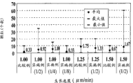
Result at experimentizing with the foregoing description and the produced silicon epitaxial wafer of the said silicon epitaxial wafer manufacture method of Comparative Examples is shown in following Fig. 7 and Fig. 8.
Fig. 7 illustrates, the vapor phase growth speed of silicon epitaxy layer (μ m/min), and, the relation in the silicon epitaxial wafer 1 between the incidence (%) of crackle.In the figure, as embodiment, what showed is 1/2 cracking frequency that the zone is residual when periphery oxide-film 110 is arranged at the peripheral part 16 of monocrystalline silicon substrate 10, and periphery oxide-film 110 has also obtained same result when residuing in 1/4,1/8 zone.
As shown in the drawing, embodiment is different with Comparative Examples, does not also crack even the speed of growth is higher.That is, can under the state that suppresses the crackle generation, go out silicon epitaxy layer with higher speed of growth vapor phase growth.
Fig. 8 illustrates, the relation between the residual ratio of the quantity (number) of the particle that is produced on 1 silicon epitaxial wafer and the vapor phase growth speed (μ m/min) of silicon epitaxy layer and periphery oxide-film 110.In the figure, the top numeric representation speed of growth (μ m/min) of transverse axis, the ratio of residual periphery oxide-film 110 in the fraction representation hydrofluoric acid treatment operation in the following bracket.
As shown in the drawing, when periphery oxide-film 110 on the peripheral part 16 of monocrystalline silicon substrate 10 residues in 1/4,1/8 the zone, the particle that is produced is below 15, reached the effect that the inhibition particle with the Comparative Examples equal extent that does not have periphery oxide-film 110 produces.Yet, when on the monocrystalline silicon substrate 10 that residues at periphery oxide-film 110 in 1/2 zone during vapor phase growth silicon epitaxy layer, having produced more dough, the generation rate of particle also increases.That is, when using periphery oxide-film 110 to residue in 1/4 during with the monocrystalline silicon substrate 10 of lower area, under the state that can be suppressed in the generation of dough with higher speed of growth vapor phase growth silicon epitaxy layer.
According to the present invention, even do not reduce the speed of growth of silicon epitaxy layer, also under the state that can be suppressed in the generation of auto-doping phenomenon, particle and crackle, vapor phase growth goes out silicon epitaxy layer on the first type surface of monocrystalline silicon substrate.
Claims (1)
1. silicon epitaxial wafer, has monocrystalline silicon substrate, be formed at this monocrystalline silicon substrate the back side silicon oxide layer and be formed at silicon epitaxy layer on the first type surface of above-mentioned monocrystalline silicon substrate, it is characterized in that, in the time of in the spot-facing portion that above-mentioned monocrystalline silicon substrate is placed on pedestal with upright state, the periphery oxide-film of outer most edge that is extended to the peripheral part of this monocrystalline silicon substrate from the above-mentioned back side of above-mentioned monocrystalline silicon substrate be formed at the zone below 1/4 of the peripheral part of above-mentioned monocrystalline silicon substrate~with zone that pedestal contacts between, described pedestal is polygonal pyramid platform shape, under the roof suspention, on the outer peripheral face of pedestal, has a plurality of spot-facing portion in the inside of the reacting furnace of epitaxially growing equipment.
Applications Claiming Priority (2)
| Application Number | Priority Date | Filing Date | Title |
|---|---|---|---|
| JP2003-143633 | 2003-05-21 | ||
| JP2003143633A JP4066881B2 (en) | 2003-05-21 | 2003-05-21 | Surface treatment method, silicon epitaxial wafer manufacturing method, and silicon epitaxial wafer |
Related Parent Applications (1)
| Application Number | Title | Priority Date | Filing Date |
|---|---|---|---|
| CNB2004100457066A Division CN100401483C (en) | 2003-05-21 | 2004-05-21 | Surface processing method, manufacturing method of silicon epitaxial wafer and silicon epitaxial wafer |
Publications (2)
| Publication Number | Publication Date |
|---|---|
| CN101271870A CN101271870A (en) | 2008-09-24 |
| CN101271870B true CN101271870B (en) | 2010-12-08 |
Family
ID=33531359
Family Applications (2)
| Application Number | Title | Priority Date | Filing Date |
|---|---|---|---|
| CN2008100955430A Active CN101271870B (en) | 2003-05-21 | 2004-05-21 | Silicon epitaxial wafer |
| CNB2004100457066A Active CN100401483C (en) | 2003-05-21 | 2004-05-21 | Surface processing method, manufacturing method of silicon epitaxial wafer and silicon epitaxial wafer |
Family Applications After (1)
| Application Number | Title | Priority Date | Filing Date |
|---|---|---|---|
| CNB2004100457066A Active CN100401483C (en) | 2003-05-21 | 2004-05-21 | Surface processing method, manufacturing method of silicon epitaxial wafer and silicon epitaxial wafer |
Country Status (4)
| Country | Link |
|---|---|
| JP (1) | JP4066881B2 (en) |
| KR (1) | KR101050679B1 (en) |
| CN (2) | CN101271870B (en) |
| TW (1) | TW200509224A (en) |
Families Citing this family (5)
| Publication number | Priority date | Publication date | Assignee | Title |
|---|---|---|---|---|
| CN100365889C (en) * | 2006-05-18 | 2008-01-30 | 中微光电子(潍坊)有限公司 | Method for preventing vertical-cavity-face emitting semiconductor laser from cracking while wet oxidation |
| CN101311340B (en) * | 2008-03-19 | 2010-06-02 | 南京国盛电子有限公司 | Method for preparing silicon inverse epitaxial wafer and special equipment thereof |
| JP5273150B2 (en) * | 2008-09-26 | 2013-08-28 | 信越半導体株式会社 | Manufacturing method of silicon epitaxial wafer |
| JP5141541B2 (en) * | 2008-12-24 | 2013-02-13 | 株式会社Sumco | Epitaxial wafer manufacturing method |
| KR101022567B1 (en) * | 2009-02-02 | 2011-03-16 | 주식회사 엘지실트론 | The method for manufacturing epitaxial wafer |
Citations (2)
| Publication number | Priority date | Publication date | Assignee | Title |
|---|---|---|---|---|
| US20010037761A1 (en) * | 2000-05-08 | 2001-11-08 | Ries Michael J. | Epitaxial silicon wafer free from autodoping and backside halo and a method and apparatus for the preparation thereof |
| US20010055863A1 (en) * | 1998-06-04 | 2001-12-27 | Masatake Nakano | Methods for manufacturing soi wafer and soi wafer |
Family Cites Families (3)
| Publication number | Priority date | Publication date | Assignee | Title |
|---|---|---|---|---|
| JPH04245431A (en) * | 1991-01-30 | 1992-09-02 | Kyushu Electron Metal Co Ltd | Method and apparatus for removal of oxide film from semiconductor substrate |
| JP2970499B2 (en) * | 1995-10-30 | 1999-11-02 | 日本電気株式会社 | Method for manufacturing semiconductor device |
| JP3727602B2 (en) * | 2002-03-11 | 2005-12-14 | 大日本スクリーン製造株式会社 | Substrate peripheral processing apparatus and substrate peripheral processing method |
-
2003
- 2003-05-21 JP JP2003143633A patent/JP4066881B2/en not_active Expired - Fee Related
-
2004
- 2004-05-11 TW TW093113228A patent/TW200509224A/en unknown
- 2004-05-17 KR KR1020040034749A patent/KR101050679B1/en active IP Right Grant
- 2004-05-21 CN CN2008100955430A patent/CN101271870B/en active Active
- 2004-05-21 CN CNB2004100457066A patent/CN100401483C/en active Active
Patent Citations (2)
| Publication number | Priority date | Publication date | Assignee | Title |
|---|---|---|---|---|
| US20010055863A1 (en) * | 1998-06-04 | 2001-12-27 | Masatake Nakano | Methods for manufacturing soi wafer and soi wafer |
| US20010037761A1 (en) * | 2000-05-08 | 2001-11-08 | Ries Michael J. | Epitaxial silicon wafer free from autodoping and backside halo and a method and apparatus for the preparation thereof |
Non-Patent Citations (3)
| Title |
|---|
| JP平1-248527A 1989.10.04 |
| JP平4-245431A 1992.09.02 |
| JP平8-279470A 1996.10.22 |
Also Published As
| Publication number | Publication date |
|---|---|
| KR101050679B1 (en) | 2011-07-22 |
| TW200509224A (en) | 2005-03-01 |
| JP4066881B2 (en) | 2008-03-26 |
| CN1574247A (en) | 2005-02-02 |
| JP2004349405A (en) | 2004-12-09 |
| TWI334167B (en) | 2010-12-01 |
| KR20040100937A (en) | 2004-12-02 |
| CN100401483C (en) | 2008-07-09 |
| CN101271870A (en) | 2008-09-24 |
Similar Documents
| Publication | Publication Date | Title |
|---|---|---|
| KR101300586B1 (en) | Silicon film formation apparatus and method for using same | |
| JP2008532315A (en) | Baffle wafer and randomly oriented polycrystalline silicon used therefor | |
| WO2009081720A1 (en) | Method for manufacturing epitaxial silicon wafer | |
| US7479187B2 (en) | Method for manufacturing silicon epitaxial wafer | |
| CN101271870B (en) | Silicon epitaxial wafer | |
| KR20170059211A (en) | Method of fabricating semiconductor device | |
| KR20190054958A (en) | Cleaning method and film forming method | |
| JP7221187B2 (en) | Film forming method and film forming apparatus | |
| TWI626730B (en) | Method of manufacturing epitaxial wafer | |
| JP2009064913A (en) | Substrate processing apparatus and method for manufacturing semiconductor device | |
| WO2011003366A1 (en) | Method for forming substrate with insulating buried layer | |
| US6965149B2 (en) | Epitaxial semiconductor wafer and a manufacturing method thereof | |
| JP2652759B2 (en) | Wafer pocket of barrel type susceptor for vapor phase growth equipment | |
| JP2002231634A (en) | Silicon epitaxial wafer and method of manufacturing the same | |
| JP5272377B2 (en) | Epitaxial wafer manufacturing method | |
| JPH08186076A (en) | Vapor phase growing method | |
| CN111719136A (en) | Substrate for MOCVD and method for growing buffer layer on substrate | |
| KR102416913B1 (en) | Semiconductor wafers with epitaxial layers | |
| JP2011187887A (en) | Method of manufacturing epitaxial wafer | |
| KR20180068618A (en) | Method of forimng a nitride semiconductor substrate | |
| JP5206613B2 (en) | Epitaxial wafer susceptor, manufacturing method thereof, and epitaxial growth apparatus using the same | |
| JP2689985B2 (en) | Semiconductor device manufacturing method and manufacturing apparatus | |
| JP2019091848A (en) | Method for cleaning component in furnace of vapor phase growth device | |
| JP2004343095A (en) | Cleaning method of heat processing equipment | |
| JPS61214515A (en) | Susceptor for semiconductor substrate |
Legal Events
| Date | Code | Title | Description |
|---|---|---|---|
| C06 | Publication | ||
| PB01 | Publication | ||
| C10 | Entry into substantive examination | ||
| SE01 | Entry into force of request for substantive examination | ||
| C14 | Grant of patent or utility model | ||
| GR01 | Patent grant |