CN101248505B - Apparatus and method for controlled particle beam manufacturing - Google Patents
Apparatus and method for controlled particle beam manufacturing Download PDFInfo
- Publication number
- CN101248505B CN101248505B CN2006800307085A CN200680030708A CN101248505B CN 101248505 B CN101248505 B CN 101248505B CN 2006800307085 A CN2006800307085 A CN 2006800307085A CN 200680030708 A CN200680030708 A CN 200680030708A CN 101248505 B CN101248505 B CN 101248505B
- Authority
- CN
- China
- Prior art keywords
- bundle
- digitlization
- chamber
- workpiece
- charged particle
- Prior art date
- Legal status (The legal status is an assumption and is not a legal conclusion. Google has not performed a legal analysis and makes no representation as to the accuracy of the status listed.)
- Expired - Fee Related
Links
- 239000002245 particle Substances 0.000 title claims abstract description 332
- 238000000034 method Methods 0.000 title claims description 284
- 238000004519 manufacturing process Methods 0.000 title description 26
- 230000008569 process Effects 0.000 claims description 103
- 238000012545 processing Methods 0.000 claims description 73
- 238000000151 deposition Methods 0.000 claims description 54
- 238000002347 injection Methods 0.000 claims description 45
- 239000007924 injection Substances 0.000 claims description 45
- 230000003287 optical effect Effects 0.000 claims description 44
- 239000000463 material Substances 0.000 claims description 43
- 230000008021 deposition Effects 0.000 claims description 42
- 230000008859 change Effects 0.000 claims description 40
- 210000003205 muscle Anatomy 0.000 claims description 40
- 238000005530 etching Methods 0.000 claims description 39
- 238000009826 distribution Methods 0.000 claims description 25
- 239000000126 substance Substances 0.000 claims description 23
- 239000007789 gas Substances 0.000 claims description 22
- 230000015572 biosynthetic process Effects 0.000 claims description 21
- 239000004065 semiconductor Substances 0.000 claims description 21
- 238000006073 displacement reaction Methods 0.000 claims description 20
- 238000000059 patterning Methods 0.000 claims description 16
- 238000012546 transfer Methods 0.000 claims description 16
- 238000012937 correction Methods 0.000 claims description 15
- 239000000758 substrate Substances 0.000 claims description 15
- 238000001514 detection method Methods 0.000 claims description 14
- 230000004075 alteration Effects 0.000 claims description 13
- XUIMIQQOPSSXEZ-UHFFFAOYSA-N Silicon Chemical compound [Si] XUIMIQQOPSSXEZ-UHFFFAOYSA-N 0.000 claims description 12
- 238000000137 annealing Methods 0.000 claims description 12
- 230000001965 increasing effect Effects 0.000 claims description 12
- 230000033001 locomotion Effects 0.000 claims description 12
- 239000010703 silicon Substances 0.000 claims description 12
- 230000005670 electromagnetic radiation Effects 0.000 claims description 11
- 229910052710 silicon Inorganic materials 0.000 claims description 11
- 230000004913 activation Effects 0.000 claims description 10
- 238000001994 activation Methods 0.000 claims description 10
- 230000006978 adaptation Effects 0.000 claims description 10
- 238000013461 design Methods 0.000 claims description 10
- 230000001902 propagating effect Effects 0.000 claims description 10
- 230000001360 synchronised effect Effects 0.000 claims description 10
- 238000002955 isolation Methods 0.000 claims description 8
- 239000011248 coating agent Substances 0.000 claims description 7
- 238000000576 coating method Methods 0.000 claims description 7
- 239000002019 doping agent Substances 0.000 claims description 7
- 230000005684 electric field Effects 0.000 claims description 7
- 238000002360 preparation method Methods 0.000 claims description 7
- 238000006243 chemical reaction Methods 0.000 claims description 6
- 238000003384 imaging method Methods 0.000 claims description 6
- 150000001875 compounds Chemical class 0.000 claims description 5
- 238000013016 damping Methods 0.000 claims description 5
- 239000012634 fragment Substances 0.000 claims description 5
- 230000007935 neutral effect Effects 0.000 claims description 5
- 230000009467 reduction Effects 0.000 claims description 5
- 238000000926 separation method Methods 0.000 claims description 5
- 229910001338 liquidmetal Inorganic materials 0.000 claims description 4
- 238000002161 passivation Methods 0.000 claims description 4
- 230000004044 response Effects 0.000 claims description 4
- OKTJSMMVPCPJKN-UHFFFAOYSA-N Carbon Chemical compound [C] OKTJSMMVPCPJKN-UHFFFAOYSA-N 0.000 claims description 3
- 238000010521 absorption reaction Methods 0.000 claims description 3
- 239000000654 additive Substances 0.000 claims description 3
- 230000000996 additive effect Effects 0.000 claims description 3
- 230000004907 flux Effects 0.000 claims description 3
- 238000012360 testing method Methods 0.000 claims description 3
- 206010010071 Coma Diseases 0.000 claims description 2
- 230000004888 barrier function Effects 0.000 claims description 2
- 239000002041 carbon nanotube Substances 0.000 claims description 2
- 229910021393 carbon nanotube Inorganic materials 0.000 claims description 2
- 230000000295 complement effect Effects 0.000 claims description 2
- 230000006835 compression Effects 0.000 claims description 2
- 238000007906 compression Methods 0.000 claims description 2
- 239000006185 dispersion Substances 0.000 claims description 2
- 239000003574 free electron Substances 0.000 claims description 2
- 238000010791 quenching Methods 0.000 claims description 2
- 230000000171 quenching effect Effects 0.000 claims description 2
- 238000004626 scanning electron microscopy Methods 0.000 claims description 2
- 238000001931 thermography Methods 0.000 claims description 2
- 238000011946 reduction process Methods 0.000 claims 5
- 239000002131 composite material Substances 0.000 claims 4
- 238000005137 deposition process Methods 0.000 claims 4
- 239000002243 precursor Substances 0.000 claims 4
- 238000005381 potential energy Methods 0.000 claims 3
- 238000003672 processing method Methods 0.000 claims 3
- 230000005611 electricity Effects 0.000 claims 2
- 238000002679 ablation Methods 0.000 claims 1
- 230000003044 adaptive effect Effects 0.000 claims 1
- 238000007664 blowing Methods 0.000 claims 1
- 230000003750 conditioning effect Effects 0.000 claims 1
- 238000005096 rolling process Methods 0.000 claims 1
- 238000005516 engineering process Methods 0.000 description 93
- 150000002500 ions Chemical class 0.000 description 54
- 235000012431 wafers Nutrition 0.000 description 19
- 229910001218 Gallium arsenide Inorganic materials 0.000 description 16
- 239000010408 film Substances 0.000 description 16
- JBRZTFJDHDCESZ-UHFFFAOYSA-N AsGa Chemical compound [As]#[Ga] JBRZTFJDHDCESZ-UHFFFAOYSA-N 0.000 description 15
- 230000008901 benefit Effects 0.000 description 15
- 230000000694 effects Effects 0.000 description 14
- 238000010899 nucleation Methods 0.000 description 11
- 230000006911 nucleation Effects 0.000 description 11
- 239000010410 layer Substances 0.000 description 10
- 238000011161 development Methods 0.000 description 9
- 230000018109 developmental process Effects 0.000 description 9
- 230000006870 function Effects 0.000 description 9
- 238000010884 ion-beam technique Methods 0.000 description 9
- 238000010586 diagram Methods 0.000 description 7
- 230000006872 improvement Effects 0.000 description 7
- 238000004377 microelectronic Methods 0.000 description 7
- 241000894007 species Species 0.000 description 7
- HEMHJVSKTPXQMS-UHFFFAOYSA-M Sodium hydroxide Chemical compound [OH-].[Na+] HEMHJVSKTPXQMS-UHFFFAOYSA-M 0.000 description 6
- 238000009434 installation Methods 0.000 description 6
- 238000005259 measurement Methods 0.000 description 6
- 238000001259 photo etching Methods 0.000 description 6
- 238000005229 chemical vapour deposition Methods 0.000 description 5
- 239000000460 chlorine Substances 0.000 description 5
- 238000011960 computer-aided design Methods 0.000 description 5
- 229910052751 metal Inorganic materials 0.000 description 5
- 239000002184 metal Substances 0.000 description 5
- 238000003801 milling Methods 0.000 description 5
- 229920002120 photoresistant polymer Polymers 0.000 description 5
- 230000005855 radiation Effects 0.000 description 5
- VYPSYNLAJGMNEJ-UHFFFAOYSA-N Silicium dioxide Chemical compound O=[Si]=O VYPSYNLAJGMNEJ-UHFFFAOYSA-N 0.000 description 4
- 230000001133 acceleration Effects 0.000 description 4
- 238000007385 chemical modification Methods 0.000 description 4
- 239000000470 constituent Substances 0.000 description 4
- 230000002950 deficient Effects 0.000 description 4
- 230000014509 gene expression Effects 0.000 description 4
- 238000011065 in-situ storage Methods 0.000 description 4
- 238000005457 optimization Methods 0.000 description 4
- 229910021420 polycrystalline silicon Inorganic materials 0.000 description 4
- 229920005591 polysilicon Polymers 0.000 description 4
- 229910004298 SiO 2 Inorganic materials 0.000 description 3
- 230000007547 defect Effects 0.000 description 3
- 230000009977 dual effect Effects 0.000 description 3
- 238000001704 evaporation Methods 0.000 description 3
- 230000008020 evaporation Effects 0.000 description 3
- 239000000203 mixture Substances 0.000 description 3
- 238000005240 physical vapour deposition Methods 0.000 description 3
- 238000001020 plasma etching Methods 0.000 description 3
- 238000004151 rapid thermal annealing Methods 0.000 description 3
- 239000000376 reactant Substances 0.000 description 3
- 238000004544 sputter deposition Methods 0.000 description 3
- 230000002123 temporal effect Effects 0.000 description 3
- WFKWXMTUELFFGS-UHFFFAOYSA-N tungsten Chemical compound [W] WFKWXMTUELFFGS-UHFFFAOYSA-N 0.000 description 3
- 229910052721 tungsten Inorganic materials 0.000 description 3
- 239000010937 tungsten Substances 0.000 description 3
- 229910021521 yttrium barium copper oxide Inorganic materials 0.000 description 3
- 241000226585 Antennaria plantaginifolia Species 0.000 description 2
- ZAMOUSCENKQFHK-UHFFFAOYSA-N Chlorine atom Chemical compound [Cl] ZAMOUSCENKQFHK-UHFFFAOYSA-N 0.000 description 2
- GQPLMRYTRLFLPF-UHFFFAOYSA-N Nitrous Oxide Chemical compound [O-][N+]#N GQPLMRYTRLFLPF-UHFFFAOYSA-N 0.000 description 2
- 238000005275 alloying Methods 0.000 description 2
- 238000004458 analytical method Methods 0.000 description 2
- 238000013459 approach Methods 0.000 description 2
- QVGXLLKOCUKJST-UHFFFAOYSA-N atomic oxygen Chemical compound [O] QVGXLLKOCUKJST-UHFFFAOYSA-N 0.000 description 2
- 229910052790 beryllium Inorganic materials 0.000 description 2
- ATBAMAFKBVZNFJ-UHFFFAOYSA-N beryllium atom Chemical compound [Be] ATBAMAFKBVZNFJ-UHFFFAOYSA-N 0.000 description 2
- 229910052801 chlorine Inorganic materials 0.000 description 2
- 238000004140 cleaning Methods 0.000 description 2
- 230000006378 damage Effects 0.000 description 2
- 230000006735 deficit Effects 0.000 description 2
- 238000003795 desorption Methods 0.000 description 2
- 238000010894 electron beam technology Methods 0.000 description 2
- 238000000609 electron-beam lithography Methods 0.000 description 2
- 239000000284 extract Substances 0.000 description 2
- 230000005669 field effect Effects 0.000 description 2
- 229910001385 heavy metal Inorganic materials 0.000 description 2
- 238000002513 implantation Methods 0.000 description 2
- 238000001459 lithography Methods 0.000 description 2
- 238000013507 mapping Methods 0.000 description 2
- 239000011159 matrix material Substances 0.000 description 2
- 230000005012 migration Effects 0.000 description 2
- 238000013508 migration Methods 0.000 description 2
- 230000004048 modification Effects 0.000 description 2
- 238000012986 modification Methods 0.000 description 2
- 238000012544 monitoring process Methods 0.000 description 2
- -1 monovalence Chemical class 0.000 description 2
- 238000010606 normalization Methods 0.000 description 2
- 230000003647 oxidation Effects 0.000 description 2
- 238000007254 oxidation reaction Methods 0.000 description 2
- 239000001301 oxygen Substances 0.000 description 2
- 229910052760 oxygen Inorganic materials 0.000 description 2
- 230000003071 parasitic effect Effects 0.000 description 2
- 238000000623 plasma-assisted chemical vapour deposition Methods 0.000 description 2
- BASFCYQUMIYNBI-UHFFFAOYSA-N platinum Chemical compound [Pt] BASFCYQUMIYNBI-UHFFFAOYSA-N 0.000 description 2
- 230000001105 regulatory effect Effects 0.000 description 2
- 230000008521 reorganization Effects 0.000 description 2
- 229920006395 saturated elastomer Polymers 0.000 description 2
- 238000007493 shaping process Methods 0.000 description 2
- 229910021332 silicide Inorganic materials 0.000 description 2
- FVBUAEGBCNSCDD-UHFFFAOYSA-N silicide(4-) Chemical compound [Si-4] FVBUAEGBCNSCDD-UHFFFAOYSA-N 0.000 description 2
- 239000000377 silicon dioxide Substances 0.000 description 2
- 235000012239 silicon dioxide Nutrition 0.000 description 2
- 239000000243 solution Substances 0.000 description 2
- 238000004528 spin coating Methods 0.000 description 2
- 230000009897 systematic effect Effects 0.000 description 2
- 238000013519 translation Methods 0.000 description 2
- 238000012935 Averaging Methods 0.000 description 1
- ZOXJGFHDIHLPTG-UHFFFAOYSA-N Boron Chemical compound [B] ZOXJGFHDIHLPTG-UHFFFAOYSA-N 0.000 description 1
- WKBOTKDWSSQWDR-UHFFFAOYSA-N Bromine atom Chemical compound [Br] WKBOTKDWSSQWDR-UHFFFAOYSA-N 0.000 description 1
- QPLDLSVMHZLSFG-UHFFFAOYSA-N Copper oxide Chemical compound [Cu]=O QPLDLSVMHZLSFG-UHFFFAOYSA-N 0.000 description 1
- 241001269238 Data Species 0.000 description 1
- 102100029012 Dysbindin Human genes 0.000 description 1
- 208000035126 Facies Diseases 0.000 description 1
- YCKRFDGAMUMZLT-UHFFFAOYSA-N Fluorine atom Chemical compound [F] YCKRFDGAMUMZLT-UHFFFAOYSA-N 0.000 description 1
- GYHNNYVSQQEPJS-UHFFFAOYSA-N Gallium Chemical compound [Ga] GYHNNYVSQQEPJS-UHFFFAOYSA-N 0.000 description 1
- 101000838672 Homo sapiens Dysbindin Proteins 0.000 description 1
- ZOKXTWBITQBERF-UHFFFAOYSA-N Molybdenum Chemical compound [Mo] ZOKXTWBITQBERF-UHFFFAOYSA-N 0.000 description 1
- 241001025261 Neoraja caerulea Species 0.000 description 1
- KWYUFKZDYYNOTN-UHFFFAOYSA-M Potassium hydroxide Chemical compound [OH-].[K+] KWYUFKZDYYNOTN-UHFFFAOYSA-M 0.000 description 1
- 208000034189 Sclerosis Diseases 0.000 description 1
- BTGZYWWSOPEHMM-UHFFFAOYSA-N [O].[Cu].[Y].[Ba] Chemical compound [O].[Cu].[Y].[Ba] BTGZYWWSOPEHMM-UHFFFAOYSA-N 0.000 description 1
- 230000009471 action Effects 0.000 description 1
- 230000002776 aggregation Effects 0.000 description 1
- 238000004220 aggregation Methods 0.000 description 1
- 229910045601 alloy Inorganic materials 0.000 description 1
- 239000000956 alloy Substances 0.000 description 1
- 230000003321 amplification Effects 0.000 description 1
- 229910052785 arsenic Inorganic materials 0.000 description 1
- RQNWIZPPADIBDY-UHFFFAOYSA-N arsenic atom Chemical compound [As] RQNWIZPPADIBDY-UHFFFAOYSA-N 0.000 description 1
- OEYOHULQRFXULB-UHFFFAOYSA-N arsenic trichloride Chemical compound Cl[As](Cl)Cl OEYOHULQRFXULB-UHFFFAOYSA-N 0.000 description 1
- 238000004380 ashing Methods 0.000 description 1
- 201000009310 astigmatism Diseases 0.000 description 1
- 210000003323 beak Anatomy 0.000 description 1
- 230000006399 behavior Effects 0.000 description 1
- 229910052796 boron Inorganic materials 0.000 description 1
- GDTBXPJZTBHREO-UHFFFAOYSA-N bromine Substances BrBr GDTBXPJZTBHREO-UHFFFAOYSA-N 0.000 description 1
- 229910052794 bromium Inorganic materials 0.000 description 1
- 229910052799 carbon Inorganic materials 0.000 description 1
- 230000015556 catabolic process Effects 0.000 description 1
- 230000001413 cellular effect Effects 0.000 description 1
- 238000003486 chemical etching Methods 0.000 description 1
- 239000003153 chemical reaction reagent Substances 0.000 description 1
- 239000003795 chemical substances by application Substances 0.000 description 1
- XOYLJNJLGBYDTH-UHFFFAOYSA-M chlorogallium Chemical compound [Ga]Cl XOYLJNJLGBYDTH-UHFFFAOYSA-M 0.000 description 1
- 239000012141 concentrate Substances 0.000 description 1
- 239000004020 conductor Substances 0.000 description 1
- 238000010276 construction Methods 0.000 description 1
- 230000001276 controlling effect Effects 0.000 description 1
- 238000007796 conventional method Methods 0.000 description 1
- 239000010949 copper Substances 0.000 description 1
- 230000007797 corrosion Effects 0.000 description 1
- 238000005260 corrosion Methods 0.000 description 1
- 230000001186 cumulative effect Effects 0.000 description 1
- 238000000354 decomposition reaction Methods 0.000 description 1
- 238000003745 diagnosis Methods 0.000 description 1
- 229910003460 diamond Inorganic materials 0.000 description 1
- 239000010432 diamond Substances 0.000 description 1
- 230000003467 diminishing effect Effects 0.000 description 1
- 230000002708 enhancing effect Effects 0.000 description 1
- 238000001914 filtration Methods 0.000 description 1
- 239000012530 fluid Substances 0.000 description 1
- 229910052731 fluorine Inorganic materials 0.000 description 1
- 239000011737 fluorine Substances 0.000 description 1
- 229910052733 gallium Inorganic materials 0.000 description 1
- UPWPDUACHOATKO-UHFFFAOYSA-K gallium trichloride Chemical compound Cl[Ga](Cl)Cl UPWPDUACHOATKO-UHFFFAOYSA-K 0.000 description 1
- CKHJYUSOUQDYEN-UHFFFAOYSA-N gallium(3+) Chemical compound [Ga+3] CKHJYUSOUQDYEN-UHFFFAOYSA-N 0.000 description 1
- XLYOFNOQVPJJNP-UHFFFAOYSA-M hydroxide Chemical compound [OH-] XLYOFNOQVPJJNP-UHFFFAOYSA-M 0.000 description 1
- 238000003780 insertion Methods 0.000 description 1
- 230000037431 insertion Effects 0.000 description 1
- 239000012212 insulator Substances 0.000 description 1
- 230000003993 interaction Effects 0.000 description 1
- 239000011229 interlayer Substances 0.000 description 1
- 238000002164 ion-beam lithography Methods 0.000 description 1
- 238000000608 laser ablation Methods 0.000 description 1
- 239000007788 liquid Substances 0.000 description 1
- 230000007774 longterm Effects 0.000 description 1
- 238000003754 machining Methods 0.000 description 1
- 230000013011 mating Effects 0.000 description 1
- 230000007246 mechanism Effects 0.000 description 1
- 230000005055 memory storage Effects 0.000 description 1
- 229910044991 metal oxide Inorganic materials 0.000 description 1
- 150000004706 metal oxides Chemical class 0.000 description 1
- 238000002156 mixing Methods 0.000 description 1
- 229910052750 molybdenum Inorganic materials 0.000 description 1
- 239000011733 molybdenum Substances 0.000 description 1
- 239000001272 nitrous oxide Substances 0.000 description 1
- 238000003199 nucleic acid amplification method Methods 0.000 description 1
- 239000013618 particulate matter Substances 0.000 description 1
- 230000010363 phase shift Effects 0.000 description 1
- 239000004033 plastic Substances 0.000 description 1
- 229920003023 plastic Polymers 0.000 description 1
- 229910052697 platinum Inorganic materials 0.000 description 1
- 238000006116 polymerization reaction Methods 0.000 description 1
- 238000007639 printing Methods 0.000 description 1
- 238000011002 quantification Methods 0.000 description 1
- 230000008439 repair process Effects 0.000 description 1
- 230000027756 respiratory electron transport chain Effects 0.000 description 1
- 238000005070 sampling Methods 0.000 description 1
- 238000004062 sedimentation Methods 0.000 description 1
- 230000011218 segmentation Effects 0.000 description 1
- 230000035945 sensitivity Effects 0.000 description 1
- 229910052814 silicon oxide Inorganic materials 0.000 description 1
- 238000004088 simulation Methods 0.000 description 1
- 239000002904 solvent Substances 0.000 description 1
- 238000004611 spectroscopical analysis Methods 0.000 description 1
- 238000003860 storage Methods 0.000 description 1
- 239000002887 superconductor Substances 0.000 description 1
- 239000000725 suspension Substances 0.000 description 1
- 229910052715 tantalum Inorganic materials 0.000 description 1
- GUVRBAGPIYLISA-UHFFFAOYSA-N tantalum atom Chemical compound [Ta] GUVRBAGPIYLISA-UHFFFAOYSA-N 0.000 description 1
- 230000002277 temperature effect Effects 0.000 description 1
- 238000007725 thermal activation Methods 0.000 description 1
- 238000000427 thin-film deposition Methods 0.000 description 1
- 210000001519 tissue Anatomy 0.000 description 1
- 230000007704 transition Effects 0.000 description 1
- 238000009966 trimming Methods 0.000 description 1
Images


Classifications
-
- H—ELECTRICITY
- H01—ELECTRIC ELEMENTS
- H01J—ELECTRIC DISCHARGE TUBES OR DISCHARGE LAMPS
- H01J37/00—Discharge tubes with provision for introducing objects or material to be exposed to the discharge, e.g. for the purpose of examination or processing thereof
- H01J37/30—Electron-beam or ion-beam tubes for localised treatment of objects
- H01J37/305—Electron-beam or ion-beam tubes for localised treatment of objects for casting, melting, evaporating, or etching
- H01J37/3053—Electron-beam or ion-beam tubes for localised treatment of objects for casting, melting, evaporating, or etching for evaporating or etching
- H01J37/3056—Electron-beam or ion-beam tubes for localised treatment of objects for casting, melting, evaporating, or etching for evaporating or etching for microworking, e. g. etching of gratings or trimming of electrical components
-
- H—ELECTRICITY
- H01—ELECTRIC ELEMENTS
- H01L—SEMICONDUCTOR DEVICES NOT COVERED BY CLASS H10
- H01L21/00—Processes or apparatus adapted for the manufacture or treatment of semiconductor or solid state devices or of parts thereof
- H01L21/02—Manufacture or treatment of semiconductor devices or of parts thereof
- H01L21/04—Manufacture or treatment of semiconductor devices or of parts thereof the devices having potential barriers, e.g. a PN junction, depletion layer or carrier concentration layer
- H01L21/18—Manufacture or treatment of semiconductor devices or of parts thereof the devices having potential barriers, e.g. a PN junction, depletion layer or carrier concentration layer the devices having semiconductor bodies comprising elements of Group IV of the Periodic Table or AIIIBV compounds with or without impurities, e.g. doping materials
- H01L21/30—Treatment of semiconductor bodies using processes or apparatus not provided for in groups H01L21/20 - H01L21/26
- H01L21/302—Treatment of semiconductor bodies using processes or apparatus not provided for in groups H01L21/20 - H01L21/26 to change their surface-physical characteristics or shape, e.g. etching, polishing, cutting
- H01L21/306—Chemical or electrical treatment, e.g. electrolytic etching
- H01L21/3065—Plasma etching; Reactive-ion etching
-
- B—PERFORMING OPERATIONS; TRANSPORTING
- B82—NANOTECHNOLOGY
- B82Y—SPECIFIC USES OR APPLICATIONS OF NANOSTRUCTURES; MEASUREMENT OR ANALYSIS OF NANOSTRUCTURES; MANUFACTURE OR TREATMENT OF NANOSTRUCTURES
- B82Y10/00—Nanotechnology for information processing, storage or transmission, e.g. quantum computing or single electron logic
-
- B—PERFORMING OPERATIONS; TRANSPORTING
- B82—NANOTECHNOLOGY
- B82Y—SPECIFIC USES OR APPLICATIONS OF NANOSTRUCTURES; MEASUREMENT OR ANALYSIS OF NANOSTRUCTURES; MANUFACTURE OR TREATMENT OF NANOSTRUCTURES
- B82Y40/00—Manufacture or treatment of nanostructures
-
- H—ELECTRICITY
- H01—ELECTRIC ELEMENTS
- H01J—ELECTRIC DISCHARGE TUBES OR DISCHARGE LAMPS
- H01J37/00—Discharge tubes with provision for introducing objects or material to be exposed to the discharge, e.g. for the purpose of examination or processing thereof
- H01J37/02—Details
- H01J37/04—Arrangements of electrodes and associated parts for generating or controlling the discharge, e.g. electron-optical arrangement or ion-optical arrangement
- H01J37/045—Beam blanking or chopping, i.e. arrangements for momentarily interrupting exposure to the discharge
-
- H—ELECTRICITY
- H01—ELECTRIC ELEMENTS
- H01J—ELECTRIC DISCHARGE TUBES OR DISCHARGE LAMPS
- H01J37/00—Discharge tubes with provision for introducing objects or material to be exposed to the discharge, e.g. for the purpose of examination or processing thereof
- H01J37/30—Electron-beam or ion-beam tubes for localised treatment of objects
- H01J37/3002—Details
- H01J37/3007—Electron or ion-optical systems
-
- H—ELECTRICITY
- H01—ELECTRIC ELEMENTS
- H01J—ELECTRIC DISCHARGE TUBES OR DISCHARGE LAMPS
- H01J37/00—Discharge tubes with provision for introducing objects or material to be exposed to the discharge, e.g. for the purpose of examination or processing thereof
- H01J37/30—Electron-beam or ion-beam tubes for localised treatment of objects
- H01J37/304—Controlling tubes by information coming from the objects or from the beam, e.g. correction signals
-
- H—ELECTRICITY
- H01—ELECTRIC ELEMENTS
- H01J—ELECTRIC DISCHARGE TUBES OR DISCHARGE LAMPS
- H01J37/00—Discharge tubes with provision for introducing objects or material to be exposed to the discharge, e.g. for the purpose of examination or processing thereof
- H01J37/30—Electron-beam or ion-beam tubes for localised treatment of objects
- H01J37/317—Electron-beam or ion-beam tubes for localised treatment of objects for changing properties of the objects or for applying thin layers thereon, e.g. for ion implantation
- H01J37/3171—Electron-beam or ion-beam tubes for localised treatment of objects for changing properties of the objects or for applying thin layers thereon, e.g. for ion implantation for ion implantation
- H01J37/3172—Maskless patterned ion implantation
-
- H—ELECTRICITY
- H01—ELECTRIC ELEMENTS
- H01J—ELECTRIC DISCHARGE TUBES OR DISCHARGE LAMPS
- H01J37/00—Discharge tubes with provision for introducing objects or material to be exposed to the discharge, e.g. for the purpose of examination or processing thereof
- H01J37/30—Electron-beam or ion-beam tubes for localised treatment of objects
- H01J37/317—Electron-beam or ion-beam tubes for localised treatment of objects for changing properties of the objects or for applying thin layers thereon, e.g. for ion implantation
- H01J37/3174—Particle-beam lithography, e.g. electron beam lithography
- H01J37/3177—Multi-beam, e.g. fly's eye, comb probe
-
- H—ELECTRICITY
- H01—ELECTRIC ELEMENTS
- H01L—SEMICONDUCTOR DEVICES NOT COVERED BY CLASS H10
- H01L21/00—Processes or apparatus adapted for the manufacture or treatment of semiconductor or solid state devices or of parts thereof
- H01L21/02—Manufacture or treatment of semiconductor devices or of parts thereof
- H01L21/04—Manufacture or treatment of semiconductor devices or of parts thereof the devices having potential barriers, e.g. a PN junction, depletion layer or carrier concentration layer
- H01L21/18—Manufacture or treatment of semiconductor devices or of parts thereof the devices having potential barriers, e.g. a PN junction, depletion layer or carrier concentration layer the devices having semiconductor bodies comprising elements of Group IV of the Periodic Table or AIIIBV compounds with or without impurities, e.g. doping materials
- H01L21/26—Bombardment with radiation
- H01L21/263—Bombardment with radiation with high-energy radiation
- H01L21/265—Bombardment with radiation with high-energy radiation producing ion implantation
- H01L21/26506—Bombardment with radiation with high-energy radiation producing ion implantation in group IV semiconductors
- H01L21/26513—Bombardment with radiation with high-energy radiation producing ion implantation in group IV semiconductors of electrically active species
-
- H—ELECTRICITY
- H01—ELECTRIC ELEMENTS
- H01L—SEMICONDUCTOR DEVICES NOT COVERED BY CLASS H10
- H01L29/00—Semiconductor devices specially adapted for rectifying, amplifying, oscillating or switching and having potential barriers; Capacitors or resistors having potential barriers, e.g. a PN-junction depletion layer or carrier concentration layer; Details of semiconductor bodies or of electrodes thereof ; Multistep manufacturing processes therefor
- H01L29/66—Types of semiconductor device ; Multistep manufacturing processes therefor
- H01L29/66007—Multistep manufacturing processes
- H01L29/66075—Multistep manufacturing processes of devices having semiconductor bodies comprising group 14 or group 13/15 materials
- H01L29/66227—Multistep manufacturing processes of devices having semiconductor bodies comprising group 14 or group 13/15 materials the devices being controllable only by the electric current supplied or the electric potential applied, to an electrode which does not carry the current to be rectified, amplified or switched, e.g. three-terminal devices
- H01L29/66409—Unipolar field-effect transistors
- H01L29/66446—Unipolar field-effect transistors with an active layer made of a group 13/15 material, e.g. group 13/15 velocity modulation transistor [VMT], group 13/15 negative resistance FET [NERFET]
- H01L29/66462—Unipolar field-effect transistors with an active layer made of a group 13/15 material, e.g. group 13/15 velocity modulation transistor [VMT], group 13/15 negative resistance FET [NERFET] with a heterojunction interface channel or gate, e.g. HFET, HIGFET, SISFET, HJFET, HEMT
-
- H—ELECTRICITY
- H01—ELECTRIC ELEMENTS
- H01L—SEMICONDUCTOR DEVICES NOT COVERED BY CLASS H10
- H01L29/00—Semiconductor devices specially adapted for rectifying, amplifying, oscillating or switching and having potential barriers; Capacitors or resistors having potential barriers, e.g. a PN-junction depletion layer or carrier concentration layer; Details of semiconductor bodies or of electrodes thereof ; Multistep manufacturing processes therefor
- H01L29/66—Types of semiconductor device ; Multistep manufacturing processes therefor
- H01L29/66007—Multistep manufacturing processes
- H01L29/66075—Multistep manufacturing processes of devices having semiconductor bodies comprising group 14 or group 13/15 materials
- H01L29/66227—Multistep manufacturing processes of devices having semiconductor bodies comprising group 14 or group 13/15 materials the devices being controllable only by the electric current supplied or the electric potential applied, to an electrode which does not carry the current to be rectified, amplified or switched, e.g. three-terminal devices
- H01L29/66409—Unipolar field-effect transistors
- H01L29/66477—Unipolar field-effect transistors with an insulated gate, i.e. MISFET
- H01L29/66568—Lateral single gate silicon transistors
- H01L29/66659—Lateral single gate silicon transistors with asymmetry in the channel direction, e.g. lateral high-voltage MISFETs with drain offset region, extended drain MISFETs
-
- H—ELECTRICITY
- H01—ELECTRIC ELEMENTS
- H01J—ELECTRIC DISCHARGE TUBES OR DISCHARGE LAMPS
- H01J2237/00—Discharge tubes exposing object to beam, e.g. for analysis treatment, etching, imaging
- H01J2237/04—Means for controlling the discharge
- H01J2237/043—Beam blanking
- H01J2237/0432—High speed and short duration
-
- H—ELECTRICITY
- H01—ELECTRIC ELEMENTS
- H01J—ELECTRIC DISCHARGE TUBES OR DISCHARGE LAMPS
- H01J2237/00—Discharge tubes exposing object to beam, e.g. for analysis treatment, etching, imaging
- H01J2237/04—Means for controlling the discharge
- H01J2237/047—Changing particle velocity
-
- H—ELECTRICITY
- H01—ELECTRIC ELEMENTS
- H01J—ELECTRIC DISCHARGE TUBES OR DISCHARGE LAMPS
- H01J2237/00—Discharge tubes exposing object to beam, e.g. for analysis treatment, etching, imaging
- H01J2237/30—Electron or ion beam tubes for processing objects
- H01J2237/304—Controlling tubes
- H01J2237/30472—Controlling the beam
-
- H—ELECTRICITY
- H01—ELECTRIC ELEMENTS
- H01J—ELECTRIC DISCHARGE TUBES OR DISCHARGE LAMPS
- H01J2237/00—Discharge tubes exposing object to beam, e.g. for analysis treatment, etching, imaging
- H01J2237/30—Electron or ion beam tubes for processing objects
- H01J2237/317—Processing objects on a microscale
- H01J2237/31701—Ion implantation
- H01J2237/31706—Ion implantation characterised by the area treated
- H01J2237/3171—Ion implantation characterised by the area treated patterned
- H01J2237/31713—Focused ion beam
-
- H—ELECTRICITY
- H01—ELECTRIC ELEMENTS
- H01J—ELECTRIC DISCHARGE TUBES OR DISCHARGE LAMPS
- H01J2237/00—Discharge tubes exposing object to beam, e.g. for analysis treatment, etching, imaging
- H01J2237/30—Electron or ion beam tubes for processing objects
- H01J2237/317—Processing objects on a microscale
- H01J2237/31732—Depositing thin layers on selected microareas
-
- H—ELECTRICITY
- H01—ELECTRIC ELEMENTS
- H01J—ELECTRIC DISCHARGE TUBES OR DISCHARGE LAMPS
- H01J2237/00—Discharge tubes exposing object to beam, e.g. for analysis treatment, etching, imaging
- H01J2237/30—Electron or ion beam tubes for processing objects
- H01J2237/317—Processing objects on a microscale
- H01J2237/31735—Direct-write microstructures
- H01J2237/31737—Direct-write microstructures using ions
-
- H—ELECTRICITY
- H01—ELECTRIC ELEMENTS
- H01J—ELECTRIC DISCHARGE TUBES OR DISCHARGE LAMPS
- H01J2237/00—Discharge tubes exposing object to beam, e.g. for analysis treatment, etching, imaging
- H01J2237/30—Electron or ion beam tubes for processing objects
- H01J2237/317—Processing objects on a microscale
- H01J2237/3174—Etching microareas
-
- H—ELECTRICITY
- H01—ELECTRIC ELEMENTS
- H01J—ELECTRIC DISCHARGE TUBES OR DISCHARGE LAMPS
- H01J2237/00—Discharge tubes exposing object to beam, e.g. for analysis treatment, etching, imaging
- H01J2237/30—Electron or ion beam tubes for processing objects
- H01J2237/317—Processing objects on a microscale
- H01J2237/31749—Focused ion beam
-
- H—ELECTRICITY
- H01—ELECTRIC ELEMENTS
- H01J—ELECTRIC DISCHARGE TUBES OR DISCHARGE LAMPS
- H01J2237/00—Discharge tubes exposing object to beam, e.g. for analysis treatment, etching, imaging
- H01J2237/30—Electron or ion beam tubes for processing objects
- H01J2237/317—Processing objects on a microscale
- H01J2237/3175—Lithography
- H01J2237/31761—Patterning strategy
- H01J2237/31766—Continuous moving of wafer
-
- H—ELECTRICITY
- H01—ELECTRIC ELEMENTS
- H01L—SEMICONDUCTOR DEVICES NOT COVERED BY CLASS H10
- H01L21/00—Processes or apparatus adapted for the manufacture or treatment of semiconductor or solid state devices or of parts thereof
- H01L21/70—Manufacture or treatment of devices consisting of a plurality of solid state components formed in or on a common substrate or of parts thereof; Manufacture of integrated circuit devices or of parts thereof
- H01L21/71—Manufacture of specific parts of devices defined in group H01L21/70
- H01L21/76—Making of isolation regions between components
- H01L21/762—Dielectric regions, e.g. EPIC dielectric isolation, LOCOS; Trench refilling techniques, SOI technology, use of channel stoppers
- H01L21/7624—Dielectric regions, e.g. EPIC dielectric isolation, LOCOS; Trench refilling techniques, SOI technology, use of channel stoppers using semiconductor on insulator [SOI] technology
- H01L21/76264—SOI together with lateral isolation, e.g. using local oxidation of silicon, or dielectric or polycristalline material refilled trench or air gap isolation regions, e.g. completely isolated semiconductor islands
- H01L21/76267—Vertical isolation by silicon implanted buried insulating layers, e.g. oxide layers, i.e. SIMOX techniques
-
- H—ELECTRICITY
- H01—ELECTRIC ELEMENTS
- H01L—SEMICONDUCTOR DEVICES NOT COVERED BY CLASS H10
- H01L21/00—Processes or apparatus adapted for the manufacture or treatment of semiconductor or solid state devices or of parts thereof
- H01L21/70—Manufacture or treatment of devices consisting of a plurality of solid state components formed in or on a common substrate or of parts thereof; Manufacture of integrated circuit devices or of parts thereof
- H01L21/77—Manufacture or treatment of devices consisting of a plurality of solid state components or integrated circuits formed in, or on, a common substrate
- H01L21/78—Manufacture or treatment of devices consisting of a plurality of solid state components or integrated circuits formed in, or on, a common substrate with subsequent division of the substrate into plural individual devices
- H01L21/82—Manufacture or treatment of devices consisting of a plurality of solid state components or integrated circuits formed in, or on, a common substrate with subsequent division of the substrate into plural individual devices to produce devices, e.g. integrated circuits, each consisting of a plurality of components
- H01L21/84—Manufacture or treatment of devices consisting of a plurality of solid state components or integrated circuits formed in, or on, a common substrate with subsequent division of the substrate into plural individual devices to produce devices, e.g. integrated circuits, each consisting of a plurality of components the substrate being other than a semiconductor body, e.g. being an insulating body
-
- H—ELECTRICITY
- H01—ELECTRIC ELEMENTS
- H01L—SEMICONDUCTOR DEVICES NOT COVERED BY CLASS H10
- H01L27/00—Devices consisting of a plurality of semiconductor or other solid-state components formed in or on a common substrate
- H01L27/02—Devices consisting of a plurality of semiconductor or other solid-state components formed in or on a common substrate including semiconductor components specially adapted for rectifying, oscillating, amplifying or switching and having potential barriers; including integrated passive circuit elements having potential barriers
- H01L27/04—Devices consisting of a plurality of semiconductor or other solid-state components formed in or on a common substrate including semiconductor components specially adapted for rectifying, oscillating, amplifying or switching and having potential barriers; including integrated passive circuit elements having potential barriers the substrate being a semiconductor body
- H01L27/06—Devices consisting of a plurality of semiconductor or other solid-state components formed in or on a common substrate including semiconductor components specially adapted for rectifying, oscillating, amplifying or switching and having potential barriers; including integrated passive circuit elements having potential barriers the substrate being a semiconductor body including a plurality of individual components in a non-repetitive configuration
- H01L27/0611—Devices consisting of a plurality of semiconductor or other solid-state components formed in or on a common substrate including semiconductor components specially adapted for rectifying, oscillating, amplifying or switching and having potential barriers; including integrated passive circuit elements having potential barriers the substrate being a semiconductor body including a plurality of individual components in a non-repetitive configuration integrated circuits having a two-dimensional layout of components without a common active region
- H01L27/0617—Devices consisting of a plurality of semiconductor or other solid-state components formed in or on a common substrate including semiconductor components specially adapted for rectifying, oscillating, amplifying or switching and having potential barriers; including integrated passive circuit elements having potential barriers the substrate being a semiconductor body including a plurality of individual components in a non-repetitive configuration integrated circuits having a two-dimensional layout of components without a common active region comprising components of the field-effect type
- H01L27/0629—Devices consisting of a plurality of semiconductor or other solid-state components formed in or on a common substrate including semiconductor components specially adapted for rectifying, oscillating, amplifying or switching and having potential barriers; including integrated passive circuit elements having potential barriers the substrate being a semiconductor body including a plurality of individual components in a non-repetitive configuration integrated circuits having a two-dimensional layout of components without a common active region comprising components of the field-effect type in combination with diodes, or resistors, or capacitors
-
- Y—GENERAL TAGGING OF NEW TECHNOLOGICAL DEVELOPMENTS; GENERAL TAGGING OF CROSS-SECTIONAL TECHNOLOGIES SPANNING OVER SEVERAL SECTIONS OF THE IPC; TECHNICAL SUBJECTS COVERED BY FORMER USPC CROSS-REFERENCE ART COLLECTIONS [XRACs] AND DIGESTS
- Y10—TECHNICAL SUBJECTS COVERED BY FORMER USPC
- Y10T—TECHNICAL SUBJECTS COVERED BY FORMER US CLASSIFICATION
- Y10T428/00—Stock material or miscellaneous articles
- Y10T428/24—Structurally defined web or sheet [e.g., overall dimension, etc.]
- Y10T428/24802—Discontinuous or differential coating, impregnation or bond [e.g., artwork, printing, retouched photograph, etc.]
- Y10T428/24893—Discontinuous or differential coating, impregnation or bond [e.g., artwork, printing, retouched photograph, etc.] including particulate material
Landscapes
- Engineering & Computer Science (AREA)
- Physics & Mathematics (AREA)
- Chemical & Material Sciences (AREA)
- Analytical Chemistry (AREA)
- Microelectronics & Electronic Packaging (AREA)
- Power Engineering (AREA)
- Manufacturing & Machinery (AREA)
- Condensed Matter Physics & Semiconductors (AREA)
- General Physics & Mathematics (AREA)
- Computer Hardware Design (AREA)
- High Energy & Nuclear Physics (AREA)
- Nanotechnology (AREA)
- Crystallography & Structural Chemistry (AREA)
- Ceramic Engineering (AREA)
- Health & Medical Sciences (AREA)
- Toxicology (AREA)
- Plasma & Fusion (AREA)
- Theoretical Computer Science (AREA)
- Mathematical Physics (AREA)
- Exposure And Positioning Against Photoresist Photosensitive Materials (AREA)
- Electron Beam Exposure (AREA)
- Powder Metallurgy (AREA)
- Particle Accelerators (AREA)
Abstract
A chamber for exposing a workpiece to charged particles includes a charged particle source for generating a stream of charged particles, a collimator configured to collimate and direct the stream of charged particles from the charged particle source along an axis, a beam digitizer downstream of the collimator configured to create a digital beam including groups of at least one charged particle by adjusting longitudinal spacing between the charged particles along the axis, a deflector downstream of the beam digitizer including a series of deflection stages disposed longitudinally along the axis to deflect the digital beams, and a workpiece stage downstream of the deflector configured to hold the workpiece.
Description
Cross reference
The sequence number under 35U.S.C. § 119 (e) that the present invention requires on July 8th, 2005 to submit is that 60/697,780 denomination of invention is the provisional application of " manufacturing of controlled ion bundle semiconductor ", this by reference integral body incorporate this paper into.
Technical field
The present invention relates to the semiconductor manufacturing, relate more specifically to be used to guide the method and apparatus of writing the semiconductor manufacturing.
Background technology
Photoetching has the patterning step of the key in most of ic manufacturing process.Resist, the photaesthesia plastics are spin-coated on the workpiece, and quilt is toasted by ultraviolet light usually in pattern and is exposed.Develop and baking for the second time after, the inertia organic film of the various processing that described surface stood by the described workpiece of opposing is partly covered.This processing comprises by wet chemical etch or by the gaseous plasma etching removes material, injects (for example wide beam injection) by ion and mixes and material additional (for example emission (lift-off)).The preparation of resist, exposure, development, cleaning, keeping and peel off and can increase by ten times number of steps need expensive equipment and facility is stable to set up, the processing of quantification and high yield.
Photoetching has had the main lithography tool that is used to handle little resist pattern to 45 nanometers (nm).Yet present and microelectronics future will need the minimum feature size below the 45nm.Although multiple photoetching technique (for example, ultraviolet, extreme ultraviolet appearance, maskless appearance, laser, phase shift, projection ion and electron beam lithography (EBL)) development can make it possible to down these sizes are being produced at high proportion, but their are all near the theoretical limit with respect to wavelength, overlapping accuracy and/or cost.Along with being advanced to the described limit, the shortcoming of every kind of technology causes a difficult problem, and the pattern defect that obtains can cause very big production loss.
Summary of the invention
In certain embodiment, be used for charged particle the chamber that workpiece exposes being comprised: charged particle source is used to generate charged particle stream; Collimater, configuration are used for along the alignment of axe and the charged particle stream of guiding from charged particle source; Be positioned at the bundle digitalizer in collimater downstream, configuration is used for forming the digitlization bundle of the group that comprises at least one charged particle by adjusting along the longitudinal pitch between the charged particle of described axis; Be positioned at the deflecting reflection device of described bundle digitalizer, comprise a series of deflection platform that vertically is provided with along described axis, with the group of the described charged particle of deflection; And the work stage that is positioned at the downstream of deflecting reflection device, configuration is used to keep described workpiece.In certain embodiments, Workpiece treating apparatus comprises selected described chamber, compartment (loadlock chamber) and process chamber from deposition, etching and temperature adjustment chamber.
In certain embodiment, be used for workpiece is processed into the state of finishing substantially from initial condition, and the equipment that does not need to remove in the described workpiece slave unit comprises compartment, exposure room and process chamber.
In certain embodiment, the method for handling workpiece in equipment comprises partly exposes with charged particle workpiece in exposure room.Described exposure comprises: form charged particle stream; With described stream along the alignment of axe and propagation; Described streaming digital is turned to the digitlization bundle, and described digitlization bundle comprises at least one charged particle; Employing is along the group of the vertical described charged particle of a series of deflection platform deflections that is provided with of described axis; Dwindle described group; And reduced group is directed on the described workpiece.
In certain embodiment, the method that is used to handle workpiece comprises: the described workpiece that exposes, described workpiece are no resist in exposure process; At the described workpiece of post-exposure processes, wherein said processing is selected from deposition, etching and short annealing; After handling, the described workpiece that exposes for the second time, described workpiece are no resist in exposure for the second time; And after exposure for the second time, described workpiece is carried out the second time handle, wherein said processing is selected from deposition, etching and short annealing.
In certain embodiment, be used at least a dopant is injected the method for workpiece, be included in guiding, change in the process of at least one parameter of described bundle, the bundle that will contain at least one ion is directed on the described workpiece.
In certain embodiment, be used for that the method for etching material comprises from the workpiece: the surface that the bundle that will contain charged particle is directed to described workpiece to be carrying out chemical modification to described surface portion, and the surface of described workpiece is in the pattern in first Room; With described workpiece transfer in second Room; And etchant is applied in the described workpiece, described etchant reacts with the part through chemical modification, so that material is removed.
In certain embodiment, the method that is used to deposit a material on the workpiece comprises: the surface that the bundle that will contain charged particle is directed to described workpiece to be carrying out chemical modification to described surface portion, and the surface of described workpiece is in the pattern in first Room; With described workpiece transfer in second Room; And etchant is applied in the described workpiece, described etchant reacts with the part through chemical modification, so that the material deposition.
For the purpose of the advantage of summing up the present invention and realizing in the prior art being had, certain target of the present invention and advantage are being described before.Of course it is to be understood that according to accordance with any particular embodiment of the present invention, do not need to realize all these purposes or advantage.So, for example, it should be appreciated by those skilled in the art that the present invention can realize or carry out as follows: with an advantage or one group of advantage as described herein or the mode of suggestion realize or optimize, and do not need to realize or optimize as described herein or other purpose or advantage of the mode of suggestion.
All these embodiment attempt to fall into protection scope of the present invention disclosed herein.These and other embodiment are conspicuous according to the following detailed description of the preferred embodiment of reference accompanying drawing for those skilled in the art, and the present invention does not attempt to limit disclosed any specific preferred embodiment.
Description of drawings
The present invention this disclosed these and other feature, aspect and advantage be described with reference to the accompanying drawing of preferred embodiment hereinafter, described preferred embodiment attempt the explanation rather than the restriction the present invention.
Figure 1A is the perspective view that is used for the typical equipment of controlled particle beams manufacturing;
Figure 1B is the schematic top plan view of the equipment of Figure 1A;
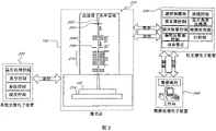
Fig. 2 is the schematic block diagram of typical charged particle exposure room;
Fig. 3 A is typical charged particle column;
The schematically illustrated charged particle pack of Fig. 3 B;
The schematically illustrated typical buncher of Fig. 3 C;
The schematically illustrated typical extinguishing means of Fig. 3 D;
What Fig. 4 A illustrated cycle in time typically writes strategy;
Fig. 4 B is the schematic block diagram of typical work stage and control electronic component;
Fig. 4 C and 4D are the schematic block diagrams of typically restrainting measuring technique;
Fig. 5 illustrates the intrafascicular typical set of charged particles of digitlization;
Fig. 6 A illustrates the schematic top plan view of deflecting reflection device;
Fig. 6 B is the fragmentary, perspective view of upper right 1/4th quadrants of the deflecting reflection device of Fig. 6 A;
Fig. 7 is the schematic block diagram of another typical charged particle column;
Fig. 8 illustrates and typically writes strategy;
The cross section of the workpiece under the various different phases of the typical digitlization bundle of the schematically illustrated assistant chemical etch process of Fig. 9 A to 9C;
The cross section of the workpiece under the various different phases of the typical digitlization bundle of the schematically illustrated assistant depositing technology of Figure 10 A to 10C;
The cross section of the workpiece under the various different phases of the schematically illustrated typical digitlization bundle injection technology of Figure 11 A to 11C;
Figure 11 E to 11I is illustrated in the typical improvement in the digitlization Shu Gaijin technical process;
Figure 12 A to 12C illustrates the typical cross section of the lightly doped drain structure of handling with the controlled particle beams;
Figure 13 A to 13B illustrates respectively the typical cross section with the lateral channel doped structure of the controlled particle beams and its doping content distribution process;
Figure 14 A to 14B illustrates the typical cross section of the heterojunction of the gate field effect tubular construction handled with the controlled particle beams of being used to insulate;
Figure 15 illustrates the gallium arsenide diode structure typical cross section of handling with the controlled particle beams in time;
Figure 16 A to 16K illustrates the typical cross section that GaAs microwave monolithic integrated circuit structure changed along with the time of being handled by the controlled particle beams;
Figure 17 illustrates the typical cross section of the heterojunction double-pole transistor of handling with the controlled particle beams;
Figure 18 illustrates the typical cross section that semiconductor structure changed along with the time of being handled by the controlled particle beams;
Figure 19 A illustrates the typical vertical view of the radioresistance structure of handling with the controlled particle beams;
Figure 19 B is the schematic cross sectional views of the radioresistance structure of Figure 19 A of obtaining along line 19B-19B;
Figure 20 illustrates the decomposition generalized section of objective lens unit;
The schematically illustrated bundle of Figure 21 A to 21G is write strategy.
Embodiment
Although hereinafter will disclose certain preferred embodiment and example,, should be appreciated that the present invention expands and surpass disclosed embodiment specifically and/or the present invention and the obvious improvement and the use of equivalent for those skilled in the art.Therefore, the restriction of the disclosed embodiment specifically under this disclosed scope of the present invention should not be subjected to hereinafter.
By obtaining littler device geometries with the direct inscription of charged particle beam.Focused ion beam (FIB) system does not have abundant ion exposure usually to support the manufacturing of high-throughput.And then only the deflection of low speed adopts existing ion optical element/deflection electronic component methodology to obtain relatively, inscribes with the effectively direct of patterned layer that prevents double conductor device.Equally, FIB has been subject to mask (for example mask) and semiconductor repairing.Along with the FIB development of technology, under the situation of not using resist, on workpiece, directly deposit simultaneously, the ability of etching and injection pattern is supported.Yet remaining problem comprises having from little and inscribes the minimum beam current density of the low energy systems of software, no tolerance system and needs and deflection speed to be supported on the photoetching under the height manufacturing scaling to the wafer that does not have (little-to-no).According to embodiment described herein for the improvement of FIB system with improve to handle and do not have in the resist processing and can obtain suitable manufacturing output at the resist of semiconductor workpiece and other media (for example, mask, CD CD, DVD CD, high definition DVD (HD DVD), Blu-ray Disc (Blue-Ray) etc.).
Advance and the physical attribute that has with the charged particle beam of the cross direction profiles of described axle can be changed with the inscription bundle that provides at a high speed, numeral (pulse) formula distributes along axis.The whole bag of tricks can be used to form by high density charged particle node and low-density (or not having density) antinode in time with the space on the ripple that defines, described ripple moves along the longitudinal path (being called " digitlization bundle " at this) of accelerated particle.For example, buncher can be used to form the partial groups (or " dodging bundle (flash) " or " bag ") of charged particle.The group of these charged particles can comprise at least one charged particle.The digitlization bundle is by the deflecting reflection device then, and thereon, the variation of voltage makes the group of described charged particle change the position with respect to the direction of propagation.The change of voltage can be carried out effective deflection thus with the timing on phase place of particle node.The sharp edge of described antinode extinguishes for directly inscribing to provide to restraint fast effectively.Described digitlization bundle is applied to surface of the work allows no resist patterned process, described no resist patterned process to comprise and/or be injected into the surface of workpiece, and/or high-resolution photoresist exposes material deposition, etching.
Figure 1A is according to the perspective view at the typical equipment 100 of this disclosed certain embodiment.Figure 1B is the vertical view of the equipment 100 of Figure 1A.Equipment 100 comprises exposure room 102, compartment 104, transportation module 106 and a plurality of process chamber 108.Although not shown, should be appreciated that equipment 100 comprises gas aggregation system and automatic processing controller, this will be described in detail hereinafter.
In certain embodiments, transportation module 106 comprises the workpiece prealigner, is in the orientation that preparation is handled so that betransported the workpiece 101 that arm 110 takes away and put into subsequently in exposure room 102 or the process chamber 108 in exposure room 102 or process chamber 108.For example, described prealigner can adopt plane, breach or other recognizable features of charge-coupled device (CCD) or other image devices location workpiece 101.In certain embodiments, described prealigner configuration is used for determining the overlapping parameter of the alignment characteristics on the workpiece 101.Described overlapping parameter can comprise x and y skew, rotation etc.
Depend on the type and the size of workpiece 101, various vacuum and conveying system can be used in the equipment 100.Can carry the optimum system choosing ground of various workpiece to adopt the high speed Work conveyance system.By on the work stage under vacuum alignment pieces rather than can increase the throughput that workpiece enters vacuum at vacuum system external alignment workpiece.The workpiece retainer of standard (for example wafer clamp) can be pumped into high vacuum in a few minutes.The aligning of workpiece 101 under vacuum can increase the throughput that wafer enters vacuum.
In certain embodiments, transportation module 106 comprises at least one processing substation, for example comprises at least one transition region, particle pollution detector, temperature quenching station and/or the tolerance station that are used for keeping workpiece 101 between treatment step.Described tolerance station can be selected from any instrument of the described type that is suitable for workpiece, described measuring station can include but not limited to EDA (energydispersive spectrometry, EDS), wavelength dispersion analyzer (WDS), ion microprobe (SIMS), scanning electron microscopy (SEM), two dimensional laser scanning imager, three-dimensional laser imaging radar (LADAR), thermal imaging system, mm-wave imaging instrument, workpiece imager and camera.
Liquid metals ion source (liquid metal ion source, LMIS) the feasible charged particle beam that forms high current density of technology.The typical technology that is used to form LMIS is heated liquid metal memory, and pin stretches out downwards from described memory.Metal is flowed along described pin by capillarity.To suck sharp tip (" taylor cone ") at the liquid on the tip of described pin from the electric field that extracts electrode, ion is sent from described tip.Described point source very bright (for example, about 10
9A/steradian/cm
2), and under suitable optical element condition, described point source allows described beam diameter little of 2nm.Various alloys provide semiconductor machining shared a plurality of ionic speciess.
The distribution energy of acceleration and focused ion can cause aberration, and described aberration causes the loss of the current density efficient of ion-optic system.Ion beam energy distributes and can measuredly make the halfwidth (FWHM) of described bundle, and can be assigned to nearly 12%.Current density efficient being provided and decomposing length item stability problem can be so that the LMIS performance be enough to satisfy the requirement of semiconductor processes instrument.An aspect among a plurality of embodiment of the present invention is to realize: charged particle beam is made up of the distribution of height energy track, and described energy track can advantageously be made up.
At least two kinds of mechanism can help the broadening of described Energy distribution: the first, about the effect of ion formation; And the second, the space-charge force after ion forms.From the emission of ions in LMIS source by the attached effect of direct field desorption of the ion on the reflector tip or by forming in field ionization by the atom of desorption from a distance, described reflector tip.The ion that generates at the tip near surface can with the neutral atom exchange charge in downstream, and force the zero energy ion at that point.Because the electric field very high (for example, between about 20 and 50 volts/nm) in described emitter region can have different energy at the ion that forms from described reflector different distance place.The Energy distribution of the described bundle of space charge effect broadening is especially under the situation of low speed.Therefore, described post 200 preferably disposes and is used for directly accelerating to described ion formation all-round afterwards.The use of low quality kind under the use of described kind is suitable situation, can be quickened by assisting ion.
Space charge effect is also by higher electric current aggravation.For the LMIS source, the width of Energy distribution preferably is proportional to the electric current at 2/3 power place.Equally, traditional LMIS source is applied to photoetching and demonstrate the behavior that is similar to electron beam.
The restriction of the maximum current density that can obtain for the system based on LMIS is caused by the Energy distribution of ion beam, and the Energy distribution of described ion beam is caused by the aberration in the top ion-optic system.Yet, the bundle digitalizer 206 that employing is positioned at the downstream of charged particle source 202 can slow down mobile particle faster effectively and can quicken to move slower particle to obtain consistent speed, and therefore every group of intrafascicular Energy distribution (accelerating voltage) that obtains unanimity of digitlization, reduce the effect of charged particle source aberration thus, shown in Fig. 3 B, described bundle Aristogrid 206 configurations are used to adjust the longitudinal separation between the charged particle, so that form the set of charged particles of decomposing along described propagation axis on time and space.
Be similar to the drift of electron beam, the unpredictable ground of LMIS taylor cone emission drifted about in the pattern in Fig. 8 about one hour cycle.Under after testing situation not, this drift may cause the displacement error of pattern.The life-span in source and current stability are the guarantees for the practical application of the production throughput handling implement that adopts traditional LMIS source.Further improvement on charged particle source 202 can provide stability and life-span, has reduced frequent source thus and has more changed jobs.The broadening that forms the Energy distribution that is associated with particle can be reduced or minimize by operating LMIS at low temperatures, reduces the neutral atom density of described tip near zone thus.Described Energy distribution also can be by the kind of selecting low evaporation to press, for example be reduced or minimize by the kind of selecting to be had the benefit of little empty radiation source by dual Ionized kind and employing, described had low charge-exchange cross section by dual Ionized kind, and on the surface of described tip, form, known have a narrow Energy distribution.
In certain embodiment, the life-time dilatation of charged particle source 202 can realize by regulated the source driving parameters before operation.Equally, the merging of automatic control program can help the life-span of charged particle source 202 and the prolongation of stability.Additionally, continuous mobile strategy (the saturated electrode type pin that for example has the tip of sclerosis), the life span that can further prolong charged particle source 202.The second level effect of the life span that process improves can comprise that emission current and positional stability improve.Source transmitting site stability can be adjusted and successfully be corrected from the Error Feedback of the Shu Chonghe of chance and to the servomotor in source by employing.Although the preferred ion beam current density is increased, the post 200 in exposure room 102 does not need to increase the current density of described bundle.
Other charged particle sources 202 also can be used to the embodiment disclosed herein.Such as but not limited to, charged particle source 202 can comprise plasma ion source (plasma ion source, PIS), volume plasma ion source (volume plasma ion source, VPIS), gas field ion source (gas field ionization source, GFIS), the carbon nano-tube field emission device, free electron laser and target, pulsed laser ablation ion source, magnetically confined plasma anode (magnetically confined plasma anode source, MAP) and the thermal field emission electron sources (thermal field emission electron source, TFE).
The collimated device 204 of charged particle stream that penetrates from charged particle source 202 is along the alignment of axe and guiding.The various collimaters 204 that comprise optical element combination are applicable to post 200.For example, in the case of unrestricted, collimater 204 can comprise at least two lens or lens and a reflective optical devices.Collimater 204 can also comprise that configuration is used for described charged particle beam is carried out the hole of shaping.Under certain embodiment, described collimator configuration is used for guiding described charged particle stream with the accelerating potential at about 5 and 30 kiloelectron-volts (keV).In certain embodiment, exposure room 102 configuration be used for about 5 and the accelerating potential of 500keV guide described charged particle stream.In certain embodiments, the voltage of collimater 204 can be attached to for example by on the auxiliary voltage that column outlet applies down.
Dispose the embodiment that is used for generating a plurality of ionic speciess at charged particle source 202, each ionic species can be selected at concrete processing application by filtering charged particle stream with particle filter (for example spectrometer filter).For example, mass-separator can dispose and be used to make selected ionic species to be deflected into the mass-separator aperture plate.Described mass-separator preferably is arranged between collimater 204 and the bundle digitalizer 206.In certain embodiments, mass-separator comprises reflective optical devices.In certain embodiments, described mass-separator comprises the ExB lens.In certain embodiments, described mass-separator comprises electromagnetic alternating field analyzer (Wein filter).
206 configurations of bundle digitalizer are used to form the digitlization bundle, and described digitlization bundle comprises at least one discrete charged particle of many groups by adjusting along the longitudinal pitch between the charged particle of propagation axis.In certain embodiment, 206 configurations of bundle digitalizer are used to form group, described group comprises about 1 to 7,000, a charged particle, about 1 to 100 between 000, a charged particle between the charged particle or about 1 to 50,000 between the charged particle, about 1 to 10,000 between 000.In certain embodiments, the configuration of bundle Aristogrid 206 be used for the Shu Yidong between the set of charged particles less than about 10 meters, less than about 1 meter, less than about 10 centimetres, less than about 10 millimeters, less than about 1 millimeter, less than about 500 microns, less than about 300 microns, less than about 100 microns, less than about 10 microns, form the longitudinal pitch D between the set of charged particles under less than about 100 nanometers, less than about 10 nanometers, less than the situation of about 1 nanometer.In certain embodiments, the configuration of bundle Aristogrid 206 is used at the Shu Hangcheng between the set of charged particles between about 1 nanometer to 10 meter, less than between about 1 nanometer to 1 meter, less than between about 1 nanometer to 10 centimetre, less than between about 1 nanometer to 10 millimeter, less than between about 1 nanometer to 1 millimeter, less than between about 1 nanometer to 500 micron, less than between about 1 nanometer to 300 micron, less than between about 1 nanometer to 100 micron, less than between about 1 nanometer to 10 micron, less than about 1 nanometer between 100 nanometers, form longitudinal pitch between the set of charged particles under the situation between 10 nanometers less than about 1 nanometer.Longitudinal pitch between described set of charged particles can be about equally, unequal, the cycle, harmonic wave etc.
In certain embodiment, bundle digitalizer 206 comprises buncher.In radio frequency (RF) buncher, charged particle stream is by the gap of described buncher, and in described gap, described charged particle is applied in alternating potential, RF or a plurality of modulated potentials waveform, claps ripple, harmonic wave, argument or its combination.Velocity modulation is compressed to described band point particle together, so that they form on the space and the time is gone up the discrete set of charged particles of decomposing.In certain embodiment, the configuration of frequency and buncher gap length is used to mate the average speed of the group of described charged particle.The electromotive force that is applied longitudinal velocity to each charged particle by described buncher the time is modulated, so that some charged particles (for example, be lower than the charged particle of average speed) be accelerated and other charged particles (for example, the charged particle that is higher than average speed) is decelerated (for example, shown in Fig. 3 B).The flight time (TOF) of the amplitude of the gap length in described buncher gap, the electromotive force that is applied and frequency and the charged particle by post 200 is determined the digitlization bundle and in the final response of the lip-deep set of charged particles of workpiece 101.
The schematically illustrated charged particle stream that moves by buncher of Fig. 3 C.The electrode 302,304 that electromotive force can pass buncher applies, and described buncher is separated by the buncher clearance G.If this after-potential is non-alternation, described charged particle begins the formation group, and described group length L and interval (spacing) D depend on described charged particle and how far moved after by described buncher.In certain embodiments, described buncher configuration is used at moving process described charged particle being compressed into described group.In certain embodiments, described buncher configuration is used to apply electric field longitudinally to compress the group of described charged particle.Described charged particle is preferably when arriving workpiece 101, in the vertical by fully compression (for example, shown in Fig. 3 C).By energy that described buncher applied can by the primary power of charged particle stream and in time and the difference between the final energy of the set of charged particles that is decomposed on the space determine.
In certain embodiment, described buncher comprises a plurality of buncher electrodes, and therefore comprises a plurality of bunchers gap.Described electromotive force can optionally be applied between two electrodes, so that change the characteristic of digitlization bundle.For example, electromotive force can, and under the situation of 3 centimetres buncher clearance G, be applied between the electrode, have the node of higher charged particle densities with formation.
Relation between buncher input parameter (for example beam energy and buncher energy, frequency and gap length) and buncher output characteristic (for example interval D, length L and density) is known.Buncher is preferably operated the charged particle that is used to every group to offer determined number.At first, it is constant that buncher gap, frequency and beam energy can be held, and electric current is adjusted.The second, beam energy and buncher electric current can be held constant, and described buncher gap, frequency are adjusted.
In certain embodiments, described buncher comprises helical coil, and described helical coil is modulated with power frequency, obtains magnetic field.In the longitudinal pitch between the circle of described coil (" gap "), the flight time (TOF) of the amplitude of the electric current that is applied and frequency and the charged particle by post 200 is determined the final response at the lip-deep digitlization bundle of workpiece 101.In certain embodiment, the longitudinal pitch configuration between frequency and the coil turn is used to mate the average speed of described digitlization bundle.
The permission of polymerization charged particle changes the dosage on the charged particle level by change buncher frequency, amplitude and duty factor writes policy optimization, and described duty factor changes the density of charged particle as mentioned above successively.Therefore, strategy adjustment is write according to described in buncher parametric optimization ground.
In certain embodiment, bundle digitalizer 206 comprises bundle extinguishing means (for example, can be enough to form the bundle extinguishing means of operating under the speed of digitlization bundle).For example, under not limited situation, the high speed extinguishing means can comprise that configuration is used for absorbing at certain intervals the aperture plate of charged particle.Described aperture plate is carried out initial alignment, so that described stream flows through the hole near the aperture plate of the internal edge of aperture plate.Electrode configuration is used for described stream is deflected into described aperture plate, described aperture plate intercepting particle flux, with form in time with the space on the digitlization bundle that decomposes.The schematically illustrated charged particle stream that moves by the high speed extinguishing means of Fig. 3 D.Aperture plate 316 is positioned near the described charged particle stream.Electrode 312,314 configuration is used for electromotive force is applied to described charged particle stream, with form in time with the space on the set of charged particles of the digitlization bundle that decomposes.If after this described electromotive force is not an alternation, charged particle continues to move with length L and interval D, and no matter how far described charged particle moves after by described high speed extinguishing means.
The embodiment of other of bundle digitalizer 206 also is fine.In certain embodiments, 206 configurations of bundle digitalizer are used to modulate the on/off state of charged particle source 202.In certain embodiments, 206 configurations of bundle digitalizer are used to modulate the lengthwise position of charged particle source 202 along axis, so that described set of charged particles is offset.
In certain embodiments, the configuration of bundle digitalizer 206 is used to apply electromagnetic radiation, for example has frequency between about 1 megahertz (MHz) and 100 gigahertz (GHZ)s (GHz) or the frequency between about 1MHz and the 25GHz.In such an embodiment, bundle digitalizer 206 can dispose the frequency of the amplitude that is used to modulate for example electromagnetic radiation, electromagnetic radiation and combination thereof etc.In certain embodiments, 206 configurations of bundle digitalizer are used for being applied to the plasma that comprises charged particle with clapping ripple.In certain embodiments, 206 configurations of bundle digitalizer are used for space charge is applied to the coda wave field.In such an embodiment, bundle digitalizer 206 can dispose and be used for resonance ground absorption space charge.In certain embodiments, 206 configurations of bundle digitalizer are used to extinguish the bundle by sucking.In certain embodiments, 206 configurations of bundle digitalizer are used for the incident neutral beam of pulsed is applied to charged particle source 202.In certain embodiments, 206 configurations of bundle digitalizer are used for pulsed laser beam is applied to charged particle source 202.
In certain embodiment, parts described here are advantageously made up.In an embodiment, post 200 comprises bundle extinguishing means that is positioned at collimater 204 downstreams and the buncher that is positioned at the downstream of described bundle extinguishing means.Can be further used in time with on the space from described bundle extinguishing means and the digitlization bundle that enters described buncher and to decompose each intrafascicular group of described digitlization.In another embodiment, post 200 comprises buncher that is positioned at collimater 204 downstreams and the bundle extinguishing means that is positioned at described buncher downstream.Other configurations also are fine.
In certain embodiment, at the average speed of the intrafascicular set of charged particles of digitlization about 1 * 10
4Meter per second (m/s) and 3 * 10
8Between the m/s.In certain embodiments, the electromotive force configuration that is applied by each deflecting electrode platform is used for the average speed of set of charged particles by described deflecting reflection device synchronous.Apply voltage during when for example, the deflecting electrode platform can dispose the group that only is used for when a charged particle under normal conditions by the deflecting reflection device and under special circumstances by specific deflecting electrode platform.In certain embodiments, the electromotive force configuration that is applied by each deflecting electrode platform is used for the average speed of set of charged particles by described deflecting reflection device synchronous in the harmonic wave mode.Apply voltage during when for example, each the deflecting electrode platform at least a portion of deflecting reflection device can dispose the group that only is used for when specific under normal conditions charged particle by the deflecting reflection device and under special circumstances by specific deflecting electrode platform.In certain embodiments, the electromotive force configuration that is applied by each deflecting electrode platform is used for the average speed of set of charged particles by described deflecting reflection device synchronous randomly.As used herein, be given to term random its most possible implication synchronously, include but not limited to, by the deflecting electrode platform voltage is applied to have on the set of charged particles of random pitch synchronously or by deflecting electrode platform at random voltage is applied to have at random or the set of charged particles of other spacings on synchronously.
In certain embodiment, when the charged particle of every group of digitlization bundle passed through, the electrode of deflection platform applied electromotive force about equally.The amount of deflection of the group of each charged particle depends on the number of electrodes that is activated in proper order.In certain embodiments, when the group of each charged particle was passed through, variable potential was applied on each deflecting electrode platform.For example, the first deflecting electrode platform has minimum voltage, and follow-up electrode has gradually the voltage that increases, along with electrode is activated and causes linear deflection.Vice versa, and in this case, the first deflecting electrode platform has maximum voltage and follow-up electrode has the voltage that reduces gradually.The quantity of the deflecting electrode platform that is activated limits the amount of deflection of the charged particle of every group of digitlization bundle.The signal time and the nominal voltage that are applied on the described deflecting reflection device can be calibrated at each deflecting electrode platform, even calibrate at each electrode in each deflecting electrode platform.The incident (" phase matched ") (for example because error, technology in the variation of charged particle speed, kind and quality, deflection platform position, pattern resolution, pattern field error, object space deflection field specifically compensate, write strategy and combination thereof etc.) of mating the charged particle of every group of digitlization bundle if desired then can postpone to trigger the voltage that is adopted of each deflecting electrode platform.In certain embodiment, the center that the circumference of the field of described deflecting electrode platform is defined as the propagation axis is offset on x or y direction less than 4mm, less than 2mm, less than 1mm or less than the inferior deflection field of 100 μ m.
In certain embodiment, the electromotive force of each deflecting electrode platform configuration is used for partly the group of described charged particle is moved towards the track of anticipation.Every group by each 1/N of the deflection distance of deflection anticipation partly in N the deflecting electrode platform.In certain embodiment, the first deflecting electrode platform or any single deflecting electrode platform configuration are used for roughly fully making at least one group of (for example whole) charged particle to move towards the track of anticipation, and other deflecting electrode platform is used to the deflection of described group of accurate adjustment.Other combination also is fine.
In certain embodiments, the deflecting reflection device that for example aforesaid quilt is synchronous harmoniously, at least a portion deflecting reflection device comprises N group deflecting electrode platform, wherein every group of deflecting electrode platform comprises N deflecting electrode, in described deflecting electrode platform, every N deflecting electrode platform configuration is used for the group of specific charged particle is moved towards the track of anticipation.If at least a portion deflecting reflection device comprises two groups of deflecting electrode platforms, then per two the deflecting electrode platforms in described group of deflecting electrode platform can dispose and be used for the group of the specific charged particle track towards anticipation is moved.If at least a portion deflecting reflection device comprises three groups of deflecting electrode platforms, then per three the deflecting electrode platform in described group of deflecting electrode platform can dispose and be used for the group of the specific charged particle track towards anticipation is moved.Other variant and configuration also are fine.
Fig. 6 A illustrates the vertical view of the deflecting reflection device 210 that is included at least one electrode in each deflecting electrode platform.The digitlization bundle configuration that comprises charged particle be used to the to flow through centre bore of deflecting reflection device 602.Described group of electrode 604,606 and 608,610 can positively charged or negative electrical charge, and the group of these charged particles is by longitudinal axis and path deflection perpendicular to the deflecting reflection device.Preferably, the electrode on relative both sides, for example electrode 604 and 606 are electrically charged opposite.Fig. 6 B is the fragmentary, perspective view of upper right 1/4th quadrants of deflecting reflection device 210.Electrode 606 is insulated part 612 in this embodiment keeps apart.The insulating part material comprises SiO
2, SiN
x, SiO
xN
yAnd combination etc.Should be appreciated that deflecting reflection device 210 can comprise a series of deflecting reflection devices, wherein each deflecting reflection device comprises at least one deflecting electrode platform, rather than single deflecting reflection device comprises a plurality of deflecting electrode platforms.For example, deflecting reflection device 210 can comprise three groups of deflecting reflection devices.Shown in Fig. 6 B, when the group of described charged particle during along path movement, they are by each deflecting electrode platform deflection.Other deflecting reflection devices and electrode configuration are fine.
In certain embodiment, 210 configurations of deflecting reflection device are used for the group of described charged particle is set into three-dimensional time space (" self adaptation virtual digit masterplate ").In certain embodiment, deflecting reflection device 210 disposes the pattern of the group of the described charged particle that is used to form cross direction profiles.In certain embodiments, deflecting reflection device 210 comprises that also configuration is used to dwindle the deflecting reflection device lens of described pattern or described virtual masterplate.Described deflecting reflection device lens can comprise electrostatic lens, electromagnetic lens, mirror lens, reflection and refraction compound lens, reflection and deflecting reflection compound lens, deflecting reflection and refraction compound lens and combination thereof etc.Fig. 7 is the theory diagram of post 200, in described block diagram, is set in the virtual digit masterplate 702 from the group of the described charged particle of deflecting reflection device 210, and the group of each charged particle is through all previous field deflection.The combination of the motion of described field deflection, home court deflection and workpiece 101 can be used to the pattern of the charged particle on the workpiece 101 is exposed.
In certain embodiment, along the phase configuration of the charged particle of described longitudinally group of digitlization bundle of axis become about equally, single harmonic, multiple harmonic, at random and combination etc.Spacing between the deflection platform can be configured to synchronous, and can be configured to the group homophase with described charged particle.In certain embodiments, the lengthwise position of deflecting electrode platform is adjustable.In certain embodiments, deflecting reflection device 210 comprises digital feedback system, and for example described digital feedback system is used to adjust the spacing between the described deflecting electrode platform.Piezoelectric elements etc. can be used to locate described electrode or deflection platform.
In certain embodiments, post 200 also comprises the objective lens unit 212 that is arranged between deflecting reflection device 210 and the work stage 214.Described objective lens unit 212 can comprise the combination of combination, deflecting electrode and refractor of combination, reflective optical devices and deflecting electrode of lens, speculum, reflective optical devices, reflective optical devices and refractor and combination thereof etc.In certain embodiments, objective lens unit 212 comprises the lens subassembly or the deflecting reflection device electrode assemblie of impairment, and the configuration of the lens subassembly of described impairment or deflecting reflection device electrode assemblie is used to dwindle, the group or the described self adaptation virtual digit masterplate of focusing and/or the described charged particle of deflection.For example, in certain but not limited embodiment, the set of charged particles with diameter (or " spot size ") of about 200nm is reduced 10 times of diameters that become about 20nm.Objective lens unit 212 also can dispose and be used for 100 times or 1000 times of described group or described masterplates.Dispose the embodiment that is used for deflection virtual digit masterplate at objective lens unit 212, described deflection can be called as " home court " deflection.In certain embodiments, the circumference of the field of objective lens unit 212 center that is defined as the propagation axis is offset on x or y direction less than 10mm, less than 5mm, less than 1mm or less than the inferior deflection field of 100 μ m.In certain embodiment, outlet comprises an outlet.
Referring again to Fig. 2, exposure room 102 comprises that work stage 214. work stage 214 configurations in the downstream that is positioned at following objective lens unit 212 are used to keep workpiece 101. preferably, work stage 214 comprises the interferometer platform, and wherein said relative position adopts optical interference to measure.Work stage 214 can be controlled the fault in enlargement that reduces in the workpiece by temperature, and described fault in enlargement may cause aliasing error.Work stage preferably is configured to move continuously, and workpiece 101 is exposed by the group of described charged particle simultaneously.For example, work stage 214 can be configured to move continuously on 25 centimetres the yardstick in 1 second cycle in exposure process.Again for example, described work stage can dispose and be used for moving exposure process paused the state that was no more than for 5 nanoseconds in per 0.5 second under.The ability of continuous exposure can increase efficient and output in travelling workpiece platform 214 without a break.
In certain embodiment, work stage 214 comprises interferometer, and described interferometer configurations is used for determining the position of work stage 214 at horizontal plane.Described x/y relative position can adopt optical interference to measure.Also can adopt additive method, for example described work stage can comprise telltale mark, grid or feature, the backscattered electron element that can be detected by ion microprobe (SIMS) or be arranged on Faraday cup below the grid of location.Described telltale mark preferably is included in and can be parallel in the assembly that post 200 moves, so that the specifically labelled working depth with respect to described workpiece is optimized, reduces post calibration and position error thus.Described digitlization bundle can be guided towards described telltale mark periodically or randomly, to check the aligning of described post.Described telltale mark also can be used to the described post 200 of calibration before the exposure workpiece, afterwards and/or in the process.
In certain embodiments, chamber 102 also comprises height control system, described height control system measuring workpieces platform 214 and/or specifically labelled height.Described height control system can comprise for example laser; A plurality of detectors, configuration are used to receive the light that sends and reflected by described workpiece from described laser; The surface that work stage 214 and/or workpiece move.Described height control system can compensate the variation of the height that measures of work stage by the lifting (for example by adopting electrostatic chuck, piezoelectric element etc.) of adjusting platform.In certain embodiments, described height control system configuration is used to compensate the height change less than 1 μ m.Electrostatic clamp can be used to be fixed to described workpiece on the work stage 214 and guarantee enough thermo-contacts and the flatness of workpiece.
Write dynamically entirely that (full motion writing FMW) can eliminate overhead time in the work stage motion of exposure during workpiece.In FMW, deflecting reflection device 210 systems upgrade in real time, to follow the trail of the motion of work stage 214, allow described system to write pattern thus when described work stage is in the motion.This optimal process ground adopts high speed optical controller (for example laser) to follow the trail of the position of work stage 214.For example, the circuit on controller can convert the laser deflection measurement of Doppler frequency shift to can be stored in the platform location register laser pulse.Interferometer, the position that laser deflection is measured or other optical technologies can be used to follow the trail of described workpiece.Therefore, the output of etching system can be improved by reducing or eliminating in the process of operation is reorientated and adjusted to platform.
In the exposure workpiece, the center of each deflection field is defined by window of opportunity (WOO).Be in the motion and deflection field when ignoring the WOO that does not inscribe in described work stage, the platform controller sends signal to tilt controller, so that initialization is carried out in exposure.During this period, described deflection system is upgraded by the work stage location register of the physical location of work stage.
Work stage can allow real-time deflection correction.By changing size or the frame size of WOO, perhaps, can dynamically optimize described system at continuous inscription by level and smooth pattern data frame by frame.Typical frame/WOO density is shown in Fig. 4 A.
Work stage can dispose and be used to provide the proper speed performance speed of 100 cels (for example with).Described work stage can dispose and be used in exposure to change (rpm) rotational workpieces up to about per minute 40,000.For example, described work stage can have as far as possible little inertia, and compatible work stage design of electrical motor can be provided.Use vacuum can compatible air bearing guide rail and linear electric machine can provide enough vibration dampings to vibration source.As additional example, described work stage motor can place vacuum system, and light material can use at described work stage, and described workpiece can be aligned on platform, eliminates described workpiece cassette and box clamping hardware thus.Additionally, three derivatives (speed, acceleration and acceleration) at first of platform position can be limited by electronic hardware and decay, correctly to control the motion of described work stage.Fig. 4 B is the schematic diagram of typical work stage and control electronic installation.
The typical application of system described herein is carried out processing of original position workpiece or resist exposure by directly inscribing on workpiece.Preferably, realize the accurate location of optical element, but displacement (WIS) error that displacement that instrument causes (TIS) and workpiece cause may cause owing to temperature effect, workpiece Treatment Effects and optical skew to target workpiece.Typical solution is the initial pattern of measuring on workpiece (for example at least one alignment mark), and with measurement data be used for accurately will new patterning image place workpiece (for example by the adjustment exposure parameter).
Alignment sensor is the various location of detection and Identification automatically and alignment key pattern, material and pattern and do not influence the quantity of exposure output preferably.The example that is used to obtain this transducer includes but not limited to: adopt high-resolution, speed positioning system for high with existing hardware; Determine the restriction and the flexibility (for example by shining upon workpiece to the location of tube core) of positioning strategy and merge the adjustment platform with tube core; And the introducing tube core is to high speed More's (grating) interferometer system of the location of tube core; And combination etc.Also can adopt other approach.
High-resolution, speed positioning system for high can adopt existing hardware, and can be similar to existing positioning of beam, but can adopt a plurality of imaging patterns.Surface with digitlization bundle scanning target (for example, location or alignment mark) produces secondary, secondary ion emission and ion sputtering.Twin shaft or cylindrical microchannel plate can be used to detect secondary electron (for example by the voltage on the biasing target voltage) and secondary ion (for example by the voltage under the biasing target voltage).Also can adopt other configuration.Image can influence each secondary ion of putting at target place and the signal productive rate of secondary electron by measuring at described bundle.The variation of the surface topology or the composition of workpiece is represented in the variation of productive rate.The position resolution of this signal is the measured beam spot size in position fixing process and the product of deflected pixels size, and is increased by the tolerance of statistics.The ion of institute's sputter provides bigger mark recognition capability, and this is because this ion can be collected and carry out quality analysis by ion microprobe (SIMS).The SIMS location technology develops finely, and can be used for mark detection and process exploitation diagnosis.Atom with spatial resolution of described beam spot size distributes and can provide very high precision for mark detects.
For the location is optimized, the product of the computer generated image of detector vision signal and described location or alignment mark can be used to strengthen or reproduce other unrecognizable echo signal from the background of strong noise.This can be by realizing to realize the enhancing of initialize signal described video gain is automatically relevant with biasing.In case described characteristic is correctly adjusted, then described signal can be associated by positioning image or the alignment mark with computer generation (CAD), so that the marking image that is enhanced to be provided.Other signals are to detect from the interaction of digitlization bundle mark.Can be used to this technology such as those signals from secondary electron and backscattered electron.Additionally, can be adopted in the differential mode from the signal of secondary electron and backscattered electron, to improve detection limit (for example, signal to noise ratio).For example, final detection signal can be the difference between SIMS and other signals.Locating speed can be limited by the localized electron device, but merging modern electronics (for example, Digital Signal Processing (DSP)) can reduce positioning time several magnitude, and does not sacrifice positioning resolution.
Quantity and the another kind in the speed in the location consider it is the configuration that was used for the register of workpiece before exposure.Depend on workpiece through regulating in advance and temperature stability in technology, multiple strategy can be used for compensation distortion and output problem.Singulated dies is aimed in the workpiece mapping usually, provide the spending of system throughput that be reduced or minimum, but the pattern deformation that unsteadiness by temperature is not caused in exposure process is proofreaied and correct.The tube core that carried out immediately before die exposure adopts four telltale marks of every grade of each tube core usually to the location (for example being used to minimize the temperature deformation effect) of tube core.This technology is eliminated the ability of inscribing with spiral fashion, has greatly been limited the output of system overhead time by memory load.Yet, on a plurality of tube cores, position simultaneously and can remain on the ability of inscribing with spiral fashion in the field that comprises a plurality of tube cores, making thus increases when reducing or minimizing pattern deformation or the maximization output.
It is more and more important that overlapping accuracy becomes along with diminishing of device geometries.For the digitlization beam tool, multistage pattern directly exposed comprises accurate interlayer location to the single workpiece that is used to make required integrated circuit.Typical workpiece alignment technology has three features: according to the generation of enough signals of the surface action of digitlization bundle; Be used to handle the detection algorithm of detected signal; And alignment characteristics process technology.
Charged particle can form medium (for example secondary electron, backscattered electron, photon and secondary ion) to the influence of workpiece, and wherein each has certain advantage on detection efficiency.Yet, select specific medium to depend on the kind of described charged particle, the energy of charged particle and the current density of described bundle for the purpose of location.Signal detector can be optimized at given medium.For example, electronic photomultiplier is generally suitable for secondary electron, and solid-state diode is generally suitable for backscattered electron, and the secondary ion mass detector is generally suitable for photon and secondary ion.
Digital signal processor processes is from the information of signal detector, so that determine the position of alignment mark.Traditional detection method comprises with digitlization Shu Jinhang one dimension line sweep.Along with the digitlization bundle passes alignment mark by the deflection migration, detected vision signal is modulated.Modulation appears because of the difference of the profile of alignment mark and workpiece.Actual alignment mark position can be by handling the distribution through the signal of ovennodulation via digital signal processing module.Another kind of detection method comprises the X/Y scan pattern of digitlization bundle, to require the video image of alignment mark.In order to obtain accurate rim detection, adopt digital signal processing algorithm.The detection at improved alignment characteristics edge realizes that by two-dimensional imaging method described method is average with the multi-frame video data, and handles the physical location of determining described alignment mark by grey scale signal.
Preferably, alignment mark happy event with equally spaced two dimensional grid on the whole working region of workpiece forms.A kind of constructive method is the structure of the multilayer semiconductor structure that is raised, and described structure constitutes silicon, silicon dioxide (SiO
2) and polysilicon layer, on the polysilicon layer of wafer, form alignment mark.In another kind of constructive method, alignment mark is etched into the surface of silicon wafer, and one deck heavy metal (for example tantalum or tungsten) is deposited in the raceway groove.The alignment mark that contains heavy metal sends the high-caliber back scattering with respect to silicon substrate, provides the profile details for low-yield back scattering ion detection thus.The selection of suitable alignment characteristics constructive method depends on by processing step indicated signal media and signal detector.
The minimum value of three alignment marks is optimised, so that accurately distinguish translation, rotation and fault in enlargement.The error that measures is fed back to the work stage control system to proofread and correct, and reduces the displacement error that workpiece and instrument cause thus.The processing of global alignment mark can allow the detection of faster and more accurate local alignment mark by removing overall error.No matter when workpiece is inserted into exposure room, and no matter when slave unit is removed workpiece, and registration process can be repeated between important treatment step etc.Also can adopt other technologies.
Patterned tool shifts a large amount of microelectronic circuit pattern datas with the form that can be operated (for example, becoming simulation from digital translation) in the short time (for example nanosecond).Described data are generally the form at ultra-large integrated (VLSI) computer-aided design (CAD), and are as described below.These data for example are used to the mobile control deflection by deflecting reflection device 210, deflecting reflection device lens, object lens 212 and/or work stage 214, and can be adjusted the aberration that is used for adjusting optical element.The charged particle exposure room may have defective (for example aberration, offset error), for example because the physical restriction of manufacturing or defective mounting and optical system.As example, if system is installed with the fine rotation with respect to work stage 214, then beam steering will be rotated with respect to the motion of work stage 214.Also can have more complicated error, for example the trial of following the trail of the outline of big square with described bundle may produce pincushion or tubular pattern.The amplitude of these effects is proportional to the amplitude of the deflection of digitlization bundle, and this can limit the size of deflection field, and can the formation system inscribes the nonlinear deformation of quality.Therefore, adopt the high-resolution inscription of digitlization bundle preferably can increase the data of conversion with the distortion of compensation deflection field, wafer distortion pattern displacement error, platform position etc.
In addition, may introduce process errors.Pattern deformation or deflection distortion may be caused by the multiple factor with digitlization bundle exposure workpiece the time.For example, in exposure room 102 or the temperature fluctuation in the workpiece 101 may cause fault in enlargement.Again for example, workpiece 101 is clamped to regularly also may causes rotation error on the work stage 214 or may cause the stress that causes image cut.And more for example, expendable non-linear pattern distortion may be caused by subsequent treatment (for example annealing).Again for example, the manufacturing of optical element or installation may be defective (for example with respect to the work stage fine rotation), and optical element has the certain physical restriction.More complicated error may cause by certain technology, such as but not limited to, follow the trail of big square with the digitlization bundle and may cause pincushion or tubular pattern.The amplitude of error may be proportional to the amplitude of beam steering, so that they can limit the size of deflection field and can the formation system inscribe the nonlinear deformation of quality.Self adaptation virtual digit masterplate is represented with software code on any given time point.Equally, when described masterplate was deflected in the home court, described masterplate can be proofreaied and correct time skew, gain, rotation and the correction of an interior non-linear pattern in time with on the space adaptively in real time.These corrections can be carried out in feature, tube core, perhaps can carry out on whole work-piece.
Digitlization bundle etching system preferably can be realized pattern and beam alignment, the sum of errors optical parallax (for example, coma, astigmatism, the pure distortion of image, aberration, spherical aberration, the curvature of field etc.) that causes with the processing of compensation on workpiece.This administration can improve the output of inscribing quality and enhanced system.
Pattern and deflection distortion problem can be integrated with in the system by electronic installation (hardware and software) that data manipulation is setovered and be corrected.For example, technology controlling and process software can adopt metrology to measure to proofread and correct the deflection of described digitlization bundle.This metrology is measured and was preferably carried out before workpiece is exposed.The quality of digitlization bundle can be in the measurement that initially is optimized to provide from the improved of follow-up tolerance or optimization.(for example shown in Fig. 4 C) in certain embodiments, the microporous mesh thing grid of blade-like is placed on the diode detector, and described grid is digitized bundle scanning.Second dervative with respect to the beam electronic current of scanning position provides high-resolution bundle profile (for example, shown in Fig. 4 D).Be optimized the focusing that (for example Automatic Optimal) allows described bundle with optical element control system halved tie profile.
In case the digitlization bundle is by with little or minimum deflection angle optimization, then proofread and correct the digitlization bundle profile in the bigger available deflection field a plurality of positions in the outer limit of the deflection field that system can be by moving to work stage 214 distortion.Then, the digitlization bundle is deflected to Shu Youhua and scans on the position at grid place.Described operation is repeated on the propagation size of deflection field.Then, other position monitoring system of Shu Youhua data and interferometer or work stage 214 can be associated.In certain embodiment, when nonlinearity erron was used as pure memory storage, the linear distribution of error was used as the argument storage.Also the distortion that depends on the bundle of inferior position in the home court can be associated.In inferior, the home court deflection that the use of grid calibration deflection distortion can be by self adaptation virtual digit masterplate to be adapting to the scanning on grid, carries out under the situation of travelling workpiece platform not.Therefore, the Automatic Optimal of bundle profile or improvement can realize in the deflection system of expansion, allow to inscribe the raising of quality and output performance thus.
Because workpiece 101 can be rotated and twist owing to handling temperature or the stress effect caused, so final measurement can be carried out before the part of workpiece 101 (for example independently tube core) is exposed.If the pattern of the pattern level before having contained is scribed on the workpiece 101, the level before then new level can be adjusted to and overlap goes up (for example three by the location tube core or four angles and adopt then and amplify or rotation correction) in each tube core.For example, calibration software can automatically be measured the feature on each die edge before exposure, and adopted to measure in aligning, processing or transmitting workpiece the arbitrary graphic pattern displacement, amplification or the rotation that are caused are proofreaied and correct.
As mentioned above, exposure room 102 can be by providing integrated circuit (IC) the design data form of CAD chart (for example with) to generate and the pattern of exposure on workpiece.The user of equipment 100 is along any specific alignment configuration and/or processing parameter output required pattern to be inscribed.In case the design (for example integrated circuit) at device is developed, a plurality of patterned layer that then can arrange described design are to cover workpiece (for example covering whole work-piece) as required.Complete exposure data preparation (EDP) bag that has user interface can be used to original design (for example with CAD or viewdata system (GDSII)) is converted to the form (for example, form (ERF) is prepared in exposure) that exposure room 102 can be used.Before being loaded into pattern data in the system, the variation of multiple form (for example similar pattern characteristics being compressed and merge and reduce the program of overlapping) can be used to increase or maximize the output of exposure room.In case described pattern data has been compressed into size that reduce or minimum, the primary and secondary deflection field that a segmentation procedure can the define pattern data and adopt level and smooth program that the density in every frame data is carried out normalization then.The acceleration of the platform when normalization has reduced to inscribe the adjacent a plurality of density pattern that repeats.After carrying out aforesaid location, pattern is not known on workpiece, adopts locator data that required bundle pattern and actual workpiece pattern are calibrated, and adopts any compensation to improve overlapping accuracy.
In various embodiments, for example the pattern data of GDSII, OASIS or other forms when is imported in the system.Then, described input data are divided into the son field, and distinguish that they are with " by inscribing " or " not inscribed ".The mapping of the son field of being inscribed is fed to the datapath module that is used for rasterisation (for example converting bitmap to).By the travelling workpiece platform, and inscribed sub-field deflection with described Shu Congyi and to a non-conterminous son of being inscribed and the son do not inscribed is exposed.Spended time is not handled the son field of not inscribed that does not have pattern data.
Can adopt various deflection techniques workpiece to be exposed with charged particle.Raster scan be bundle on whole work-piece backward and the scan pattern that moves forward; Described bundle is connected on the appointed area and is turned off up to next appointed area.Vector scan is the scan pattern that the digitlization bundle only scans selecteed zone, and on described selecteed zone, pattern will be placed; After the scanning in selected zone was finished, described bundle was turned off and is moved to the selected zone of generation scanning.Mixing the vector grating technology, to be used for the vector of the home court between the datagram case field approximate, and adopt a wide dark scanning technique deflection interior Gauss or the digitlization bundle of shaping.Output improves can be by only work stage being moved on the position of accepting exposure.The vector grating of another kind of form is included in the deflection vector in the home court, the deflection vector between the pattern characteristics in inferior, and the raster image of the feature in inferior.An amount of ability of vector optical-mechanical system can provide the output higher than pure raster scanning system, and the rasterization capability of vector optical-mechanical system allows good pattern fidelity and the high electric current with little time of staying.
As mentioned above, in certain preferred embodiment, the inferior field deflection of digitlization bundle realizes by the deflecting reflection device, why feasible this be because, on the space of the group of described charged particle and temporal longitudinal pitch allow every group independent deflection.In certain embodiment, put on each deflecting electrode platform voltage by timing with the speeds match of the group of each charged particle.
Spacing between the group of described charged particle can provide effectively to be extinguished.Especially, this extinguishing between group adopted continuous or near the fluxoid of continuous band point particle flux effectively.Temporal spacing between group allows offset error to proofread and correct (the error correction signal summation can compensate layout, deflection aberration, optical aberration and the WriteMode of platform and handle adjustment).The improvement of output can maximize by the time to digitlization bundle exposure workpiece and realize.
In certain preferred embodiment, the digitlization bundle can be realized multiple pattern exposure strategy.This strategy can be designed for beam energy, described group beam energy in batch and the beam energy that is used for self adaptation virtual digit masterplate of the group of revising exposure dose, kind, pattern quality, each charged particle.Equipment also can be discretely at specific beam energy, described group beam energy in batch and the beam energy that is used for self adaptation virtual digit masterplate of writing the group of modification exposure dose in the strategy, kind, pattern quality, each charged particle, to optimize the specific strategy of writing of specific technology.
In writing the implementation of strategies example, the whole zone that bundle passes workpiece in the mode of grating is scanned.In certain embodiment, the size of bundle spot is greater than the grid distance in the grating (for example, shown in Figure 21 A).In certain embodiment, the size of bundle spot is substantially equal to the grid distance (for example, shown in Figure 21 B) in the grating.That is, described pattern is the vector that is scanned in the vector that is scanned in the home court, inferior and the grating that is scanned in the single passage in feature to be exposed.When carrying out etching, injection and deposition, the dosage that can adjust each pixel with the characteristic processing of digitlization Shu Jinhang changes, to improve the quality of edge feature.In certain embodiments, the displacement of the group that the digitlization beam spot size greater than one and the ratio of pixel can average described charged particles, and can reduce the exposure process error.Big digitlization bundle class size improves the roughness at line edge with the ratio of pixel, and allows because the higher dosage deposition that the cumulative dose of the bundle that overlaps causes.This technology also can be carried out under the situation of resist resist being arranged or do not have.
In another embodiment that writes strategy, carry out the rapid alternation of row and column with the ratio of big spot size and little Pixel Dimensions.Produce and the same wide pixel exposure half-breadth of selected feature with digitlization bundle exposure pixel alternately, be increased in the critical dimension (for example, shown in Figure 21 C) of two features on the desired value on the axle thus.That is the grating that is scanned in the described pattern pixel that to be the vector that is scanned in the vector that is scanned in the home court, inferior and the quilt in the single passage in feature to be exposed replace along x and y direction.The quantity of the charged particle by reducing each moment effectively, output is increased, but has sacrificed the cost of critical dimension control.For adopting this inscription pattern to have advantage, for example when not having resist etching, injection and depositing operation, each pixel dosage is changed or the exposure of multiple class is used to improve device performance, edge feature quality and output at the digitlization bundle.Because system throughput is along with the square of effective inscription grid increases, so the raising of output may be very big.This technology can be carried out under the situation of resist resist being arranged or do not have.
And another embodiment that writes strategy will separate with pixel separation matrix (or " constituent "), and will be in series of passages the exposure of combination of the constituent that intersects of interlacing overlapping, each passage along x and y direction all with other the fragment of a write address of channel offset.That is, described pattern is that the vector that is scanned in the vector that is scanned in the home court, inferior and the pixel that makes in feature to be exposed are intersected the grating that is scanned in the series of passages of interlacing.The bundle size can be configured to than the big 25-100% of Pixel Dimensions, so that restraint averaging to dodging, and reduces by every group number of charged particles (for example, shown in Figure 21 D).The bigger beam spot size of Pixel Dimensions helps to reduce the roughness at line edge by systematic error is averaged relatively, to allow bigger dosage deposition (for example, shown in Figure 21 E).Should the inscription pattern have advantage at digitlization Shu Caiyong, for example can be when carrying out direct etching, injection and depositing operation, the variation of each pixel dosage is used to improve the edge feature quality, improve the edge feature quality thus.This technology also can be carried out under the condition of resist resist being arranged or do not have.Characteristic mass is enhanced, but a plurality of passages are realized under or the situation that not have to influence very little to output influence.
Another embodiment realization of writing strategy has the sampling matrix of the cellular array of predetermined Input Address size.Each passage produces the inscription grid that is limited by the distance between the beam displacement in the single passage.That is, described pattern is the vector that is scanned in the vector that is scanned in the home court, inferior and makes pixel intersect the grating that is scanned in the series of passages of a plurality of skew constituent characteristic patterns of interlacing along x and the skew of y direction with formation in feature to be exposed.The constituent of all passages forms effective exposure grid (for example, shown in Figure 21 F).The dosage of described bundle also can freely be changed in the operation envelope of system.Should the inscription pattern have advantage at digitlization Shu Caiyong, for example can be when carrying out direct etching, injection and depositing operation, the variation of each pixel dosage is used to improve the edge feature quality, improve the edge feature quality thus.This technology also can be carried out under the pixel rate greater than about 400MHz resist being arranged or do not have under the condition of resist.Well balanced between characteristic mass and output can realize thus.Change (for example, shown in Figure 21 G) in the operation envelope that the dosage of described bundle also can limit in the technology of system.This can realize with multiple technologies, and described technology comprises modulated the work period of buncher.Multistage pixel intensity is provided from 0% to 100% of beam intensity.The pixel of part intensity is used along edge feature, so that described edge is positioned between the line of Descartes's raster scan grid.Dose-modulated can be specified via the pattern data file by the user.Handle to adopt this inscription pattern to have advantage at the digitlization bundle, for example can be when not having resist etching, injection and depositing operation, the variation of each pixel dosage is used to improve the edge feature quality, improve the edge feature quality thus.This technology also can be carried out under the condition of resist resist being arranged or do not have.Well balanced between characteristic mass and output can realize thus.
Fig. 8 illustrates and adopts the typical vector grating of digitlization bundle to write strategy.Workpiece is divided into square pixel 1 to 44.Shu Tongchang passes workpiece with spiralling and inscribes, and from 1 to 4, then from 5 to 12, then from 13 to 22 etc.Each pixel is divided into band, and each band is divided into the field, and described field is divided into the son field.Described Shu Tongchang passes the inscription of each band, field and son with spiralling.In each son field, described bundle can only be inscribed on the position that the feature of being inscribed exists.Be similar to vector scan, the digitlization bundle only scans selected zone, but described bundle does not need to be turned off for moving to another zone, and the time that described at least bundle is turned off reduces owing to the dead band between the group of described charged particle can be used for this purpose.
Along with reducing of device geometries, has accurate overlapping patterning preferably at least than minimum dimension or the low magnitude of critical dimension.Workpiece is handled and is transported the error that may cause the pattern on workpiece, and described error has contribution for displacement error, especially when physical dimension falls into below 0.25 micron.Yet the patterning equipment (exposure room that for example has the digitlization bundle) of series connection has the flexibility that is used for increasing by location and pattern data these errors of correction.The tolerance program requires described digitlization bundle from alignment fully automatically, horizontal deflection/the workpiece of going forward side by side is located calibration, and wafer pattern distortion proofreaied and correct, described tolerance program fully automatically not only can be eliminated the pattern defect on level recently, and can eliminate other pattern errors.
As mentioned above, bundle measurement and laser interferometer system have several dusts with interior precision.Use these to measure, system calibration software can be collected deflection gain, the linearity, skew and the rotation at the primary and secondary deflection field.Described deflection is calibrated by laser interferometer, and the yaw motion that runs well and the distribution of the digitlization bundle in deflection field are provided.Described digitlization bundle distributes also can measured and correction with respect to the linearity of described beam steering and nonlinearity erron.Because each tube core was positioned before exposure, so can by increase to the correction of pattern software and under the state that is corrected this tube core of exposure, and carry out temperature-compensating, the described temperature-compensating system that makes reduces or eliminates pattern deformation, and described pattern deformation is caused by annealing, vacuum radiation leakage and evaporation and incorrect adjusting.
The flexibility of electronic data preparation (EDP) software allows pattern to change the changing capability of handling to obtain.The flexibility that pattern editor, tone reversal and feature skew will increase offers the user of equipment 100.In addition, characteristic boundary, can under little physical dimension, improve digitlization bundle assistant chemical etching (DBACE) and digitlization Shu Chenghe deposition (DBND) according to the dosage of size and according to the dosage of type.
Preferably, the data manipulation offset system for example will be applied to the pattern data of optical element control system through the data of overcorrect by increasing, and pattern and deflection distortion are proofreaied and correct.The data operator system applied deflection for final pattern data before optical element control, and therefore can comprise very fast electronic component (for example, the fastest electronic component in the system).This system is added to pattern data correction, deflection distortion correction and work stage motion correction the front end of optical element control system.Digital analog converter on the front end of described optical element control system will be changed from the digital signal of data operator.In a single day these analog signals are exaggerated, and then drive post 200.
Overlapping accuracy can limit submicron lithography.For example, traditional etching system can not be proofreaied and correct the distortion of the non-linear pattern that caused by processing of wafers, and the reducing of this increase by workpiece size and device geometries aggravates.Yet, can not change in exposure process because described pattern is fixed on the mask, so certain digitlization beam system described herein can advantageously be proofreaied and correct these errors.Self adaptation virtual digit masterplate is on temporal any set point with the form of software code.Therefore, in the home court, in the deflection, can proofread and correct in real time adaptively for biasing, gain, rotation and the correction of inferior interior non-linear pattern in time with on the space.These corrections can or be carried out in entire wafer at feature, tube core.
The method of handling workpiece 101 in exposure room 102 comprises the digitlization Shu Jinhang exposure of workpiece 101 with charged particle.In certain embodiment, workpiece 101 exposed to be comprised: form charged particle stream; With described stream along the alignment of axe and propagation; Described streaming digital is turned to the digitlization bundle, and described digitlization bundle comprises group (or bag or sudden strain of a muscle bundle), and described group comprises at least one charged particle; Employing is along the group of the vertical described charged particle of a series of deflection platform deflections that is provided with of described axis; Dwindle described group; And the group of reduced charged particle focused on the workpiece 101.Exposure dose is preferably less than about 1 * 10
17Individual charged particle/centimetre
2. as mentioned above, for example can comprise pack, extinguish and combination etc. at a high speed described Shu Jinhang digitlization.
In certain embodiments, the group deflection with described charged particle comprises that voltage is optionally striden across the deflecting electrode platform to be applied on each deflecting electrode platform.Optionally applying voltage can comprise to the first deflecting electrode platform and apply big voltage and apply less voltage for other deflecting electrode platforms.Optionally applying voltage also can comprise to the first deflecting electrode platform and apply small voltage and apply bigger voltage for other deflecting electrode platforms.Optionally applying voltage also can be included on each deflecting electrode platform and apply approximately equalised voltage.The dwindling of the group of described charged particle preferably produces less than about 200nm, less than about 50nm, less than about 10nm, less than about 5nm or less than the about bag diameter of 1nm.Described work stage can move in exposure process continuously.For example, described work stage can move in 1 second time cycle on the yardstick of about 100cm continuously.Again for example, described work stage can be no more than the mode of 5 nanoseconds to pause in per 0.5 second and moves.
Fig. 5 illustrates the group 502,504 of a plurality of charged particles.In certain embodiments, occur in the dead band 512 of the deflection of set of charged particles on workpiece, so that not exposure appearance in deflection.The rise time 509 of saturated beam pulse can be used for blank and edge non-blank-white.In certain embodiments, the physical dimension of the group of described charged particle is Gauss on perpendicular to the x of time and y dimension, and also is Gauss for the speed of propagating axis.In certain embodiments (for example, as shown in Figure 5), the trapezoid cross section that the group 502,504 of described charged particle has along the longitudinal axis.In Fig. 5, the group 502 and 504 of two charged particles is illustrated.Each digitlization bundle has density distribution rise time 506 and fall time 508.Time between the peak density that does not have electric charge charged particle and charged particle is the fast-pulse rise time 509.The time that has the peak density place of charged particle for every group 502,504 is between the digitized sudden strain of a muscle bundle light time 510.In the full concentration of charged particle with not have the time between the charged particle be quick fall time 511.The time that does not have charged particle is dead band 512 (antinode zone).Time between the last moment of the charged particle of the initial concentration in the charged particle of the full concentration in first group (for example organizing 502) and the subsequent group (for example organizing 504) is deflection period 514.Time between the charged particle of the initial concentration in the charged particle of first concentration in first group (for example organizing 502) and second subsequent group (for example organizing 504) is to dodge to restraint the light work period (or " dodging bundle hot spot speed ") 516, and is used for the deflection period of a time interior feature to feature.Yet, in certain embodiments, on a plurality of duty cycle, can occur extinguishing.Can adopt extinguishing means.
Referring again to Figure 1A and 1B, equipment 100 can also comprise at least one special-purpose process chamber 108.Additional process chamber can according to circumstances be used for processing in advance.Process chamber 108 can comprise the workpiece processing equipment of any kind.Such as but not limited to, process chamber 108 can comprise etching, deposition (for example oxidation, nucleation etc.), rapid thermal annealing (RTA) and combination thereof etc.Some process chambers 108 can dispose and be used for handling the workpiece 101 that has been exposed at exposure room 102, and simultaneously other process chamber 108 can dispose and be used for before or after other process chambers 108 are handled, workpiece 101 is handled before the processing of exposure room 108 etc. the time.In certain embodiment, process chamber 108 can comprise calibration or measurement facility.In certain embodiment, equipment 100 comprises a plurality of process chambers 108, so that workpiece 101 can be transformed into the product of roughly finishing from naked substrate.Preferably, workpiece 101 can be handled fully, and is not removed in the slave unit 100.In certain embodiment, from begin to make substrate to the duration of roughly finishing product less than a week, more preferably less than two days, or even more preferably less than one day, perhaps more preferably less than one hour.
In typical embodiment, two process chambers 108 are specifically designed to nucleation and oxide deposition, and the 3rd process chamber 108 is specifically designed to rapid thermal annealing, and the 4th process chamber 108 is specifically designed to chemical auxiliary figure beam etching (CADBE).Be used to carry out all these processing although a process chamber 108 can dispose, contribution allows, and for example adopts firm material to avoid the corrosion in the CADBE chamber.
Automatically process software can be used to monitor and analyze the systematic function of all aspects, carrying out the automatic control of all functions operation, and each technology that is realized by system is optimized.Software can carry out the data collection program on all the sensors of system, and described result's tissue is become report operation and state performance-relevant reading system.Software also can prepare mabage report at each workpiece of the processing of the system by comprising the target process of comparing with actual process, and described report can be used to determine defect analysis and handle the border.Processing parameter is fed back into the automatic control ring program of knowledge (for example based on) allows on stream high leverage.Software can merge the data of collecting from least one metrology process to strengthen this process exploitation, for example is used for monitoring and adjusts etch-rate, deposit thickness and pollution.Although pattern exposure can be by pattern generation system control, software can preferably move all systemic-functions, comprises treatment process, at the processing parameter of each operation etc.Also can adopt other configurations.In certain embodiment, also adopt the user to control and adjust.
Etching is to be used for the processing that semiconductor circuit is made.The microelectronic integrated circuit of high lever (leverage) utilizes the high-resolution etching of the material in critical dimension and position usually.The etching metal of the accurate control on depths of features, consistency, anisotropy and reproducibility, partly lead with dielectric and need for many application.Standard process techniques typically utilizes the patterning step relevant with resist to remove to carry out material, and wet or dry chemical etch is followed after the described patterning step relevant with resist.
The resist patterning has limited pattern, size, the degree of depth and the consistency of etch process.Do not used resist by the high-resolution removal that provides material through the milling after the ion beam exposure that focuses on or etching.Yet high dose and low sensitivity cause the deceleration of equipment, and milling does not also successfully realize commercial.Chemistry auxiliary process (for example, chemically assisted ion beam etching (CAIBE) and reactive ion etching (RIE)) is introduced into to strengthen milling, still because a plurality of parts in gas and the exposure room react, so they can not be integrated with in the FIB equipment.On the contrary, as described here, and provide quality pattern and high-throughput in the low dosage technology that can combine with the charged particle that concentrates in the group of the processing compatibility of no resist.
In certain embodiment, the etching of workpiece, injection and deposition can be carried out at exposure room 102.The multiple activation that is digitized bundle and the exposure of processing gas can greatly improve the efficient of all three kinds of technologies.From the angle of energy, kind and electric current is that the parameter of the specific described digitlization bundle of the custom-designed digitlization Shu Yinwei of technology is adjustable and can realize that described digitlization bundle can influence and decompose a part of process gas molecule.Through the atomic surface of the molecules strike workpiece that decomposes with new atom sputtering or inject workpiece, perhaps with new atomic deposition at surface of the work.In certain embodiments, the part of workpiece and/or all in exposure process, be heated.
The new family of etching technique is ideally suited in the high-resolution that adopts no resist technology, the microelectronics manufacturing of high-throughput.This new technology family is called as the digitlization bundle assistant chemical moment (DBACE) and reaches 10 to 100 times than milling to the ion exposure is responsive.Described technology comprises at least two steps, and described step comprises exposes pattern to treating on the etched zone with the digitlization bundle.The target surface of workpiece forms for the chemical reagents reaction zone with very low dosage ion energy exposure.Then, workpiece is introduced in the reacting gas in the isolation ward.Therefore, the high-resolution dry chemical etch process is removed the material in the desired position actively, and as the parallel process that is used for the exposure on digitlization bundle pattern other workpiece in exposure room.As example, DBACE can have chlorine (Cl
2) or fluorine gas (F
2) silicon and silicon dioxide (SiO
2) go up, have Cl
2GaAs (GaAs) go up, have oxygen (O for example
2) nitrous oxide (N
2O
3) carbon (for example diamond) go up, have three fluorocarbons bromine (CBrF
3) tungsten and molybdenum on and have the high-temperature superconductor thing of wet type hydroxide chemical substance (for example NaOH (NaOH), potassium hydroxide (KOH)) (for example, cuprate be as La
1.85Ba
0.15CuO
4, YBa
2Cu
3O
7-x(yttrium barium copper oxide, YBCO, Y123, yttrium barium cuprate) and the perovskite copper oxygen pottery that has or do not have normal metallic region) on carry out.DBACE successfully has been applied to the grid recessed devices of etching GaAs field effect transistor (FET) and has not been destroyed potential active device zone.
The schematically illustrated typical digitlization bundle assistant chemical etch process of Fig. 9 A-9C.In Fig. 9 A, oxide skin(coating) 902 has been deposited on the GaAs.In Fig. 9 B, oxide skin(coating) 902 in exposure room 102 by gallium ion (Ga for example
+) exposure, shown in arrow 904.Then, workpiece is transferred to the etchant chamber.In Fig. 9 C, chlorine (Cl
2) etching removes the oxide skin(coating) be exposed in exposure room 102, and respectively with gallium chloride (GaCl
2) and arsenic chloride (AsCl
2) the potential gallium and the arsenic of form.The result obtains the groove in the GaAs, shown in Fig. 9 C.The ionic species and the etch species that should be appreciated that other can depend on and treat that etched material selects.
Thin film deposition has become the conventional process in the microelectronics processing.Many technology have been used to deposit film, comprise evaporation, physical vapor deposition (PVD) (for example sputtering sedimentation), chemical vapor deposition (CVD), atomic laser deposition (ALD), electroplate (for example metallide) and apply (for example spin coating).In the processing of routine, these technology are deposited on material on the whole surface of workpiece usually, and by adopting lifting of resist Patternized technique or milling process that material is formed pattern.Because cost, complexity and the physical restriction of resist Patternized technique, other no resist technology is preferred usually in semiconductor technology.Deposition technique can by before using depositing operation, among or expose with the particle beams afterwards and advantageously avoid the resist Patternized technique, described deposition technique comprises the particle beams and thermal activation deposition, such as but not limited to, digitlization bundle activation CVD, digitlization bundle heat of activation nucleation, digitlization bundle activation ALD and chemical auxiliary figure bundle deposition.
Directly two examples of pattern deposition are ion beam nucleation deposition (IBND) and chemical assisting ion bundle deposition (CAIBD).Two kinds of technology are decomposed the lip-deep atom of workpiece or are made the lip-deep atom nucleation of workpiece, but can be restrainted the inscription technology slowly limits.CAIBD is described with respect to the advantage that adopts the digitlization bundle above, but it can be without digitlization Shu Shixian.IBND is many PVD/CVD technology, and in described technology, organic gas is introduced on the workpiece after by particle beams exposure.Growth occurs from nucleation (exposure) position that is similar to ALD.IBND usually adopts approximately the dosage than low five magnitudes of CAIBD, and this can make IBND than CAIBD fast 100,000 times.
In-situ deposition technology is that machine silicon complementary metal oxide semiconductors (CMOS) (CMOS), GaAs and other devices provide various required materials.Yet deposition output and film quality all require very high for these technologies.Before IBND, the rational output deposition of wafer process can not adopt the original position bundle to handle.As example, adopt heavy ion dosage (for example 4 * 10
6Ions/cm
2) the film deposition rate of CAIBD will be restricted to about 100A/cm by beam electronic current
2, the thick layer of 500 dusts that deposits a square centimeter will expend above 20 years.Yet IBND can produce required film thickness, also satisfies output and relationship between quality simultaneously.For example, workpiece (the about 200cm that causes the 300mm diameter
2) usable surface covered 30% technology by the deposition materials of 2.5 dusts and will expend about 5 seconds and have 10A/cm with employing
2 Exposure room 102 exposure of beam current density, this can be at 10cm
2On the magnitude of/s nucleation site is exposed.Then, workpiece can be transported to the nucleation chamber that is used for depositing, and another workpiece is exposed in exposure room 102 simultaneously.
The schematically illustrated typical digitlization bundle assistant depositing technology of Figure 10 A-10C.Begin with the untreated work-piece among Figure 10 A, the part of described workpiece is by the set of charged particles exposure of the digitlization bundle of 1002 expressions of the arrow among Figure 10 B.Then, workpiece is transferred to the settling chamber, and in described settling chamber, it is by reactant (for example reactant fluid, preferred reaction agent gas) exposure.Described reactant with react through exposed areas so that material nucleation or deposition automatically, the result obtains having the workpiece of Figure 10 C in the zone 1104 of the material that is deposited.
The flowability that the integrated micro manufacturing of silicon, GaAs and other electronic devices adopts ion to be infused in change device on the transistor adjoining edge distributes.Traditional injection technique generally includes resist deposition, patterning, development and baking, is that ion injects afterwards, resist removes (for example by ashing and/or peel off) and clean.Device fabrication adopts a series of these injection techniques, needs a large amount of patterning step thus.Patterning can be reduced by adopting serial to inject, but be used for gradient inject, lightly doped drain (LDD) and inject the device that merges altogether and can obtain more performance, and be generally the performance of increase device and simplify technology.For example, the displacement accuracy of high-resolution injection can cause the increase of device reliability and/or technology robustness.The device that the output restriction that is associated with traditional injection technique is required a large amount of injections worsens.The CMOS technology that adopts routine is as example, and injecting (that is, resist deposition, patterning, development and baking are that ion injects, resist is removed and cleaning afterwards) separately may need about 70 processing steps.Therefore, the cost of the electronic device of high lever of future generation is very high.
The exploitation of this injecting scheme can be carried out with low especially cost.For example, the processing of the mask that uses in the resist patterning step may spend a plurality of months and ten hundreds of dollars.Process exploitation (the resist conditions of exposure that for example, is suitable for mask, resist type, resist thickness etc.) may expend a plurality of months again.In case exploitation is finished, guiding processing may spend many weeks or many months.If test exposure the defective in mask design or processing step, then described technology may need to start anew, and can be formed reliably to function element repeatedly always.This long-term exploitation is unpractiaca or or even impossible (for example, the specific military device of the limited device of production quantity) for certain device.
Adopt the direct inscription injection of no resist can provide manufacturing flexibility and rapid development time to produce and the environment facies combination of production fully with advanced technology (for example, single-stage gradient injection, LDD and common injection), the guiding that will study.This system can obtain to distribute with interior, the vertical injection of scope from about 5 kilo electron volts (keV) to about 500keV at for example about 20nm.These systems can have flexibility, and with the kind of selecting ion beam with described bundle is placed in himself the 9nm of gradient energy or dose distribution, this can be used to realize advanced injection technology, for example single-stage gradient injection, LDD and common injection.
Figure 11 A directly inscribes the cross section that injects the workpiece of handling to the schematically illustrated process of 11D.Begin with the untreated work-piece among Figure 11 A, described workpiece is injected by the 1100 first group of represented digitlization bundle exposure distribution of the arrow among Figure 11 B.The result obtains having the workpiece of Figure 11 C in the zone 1102 of dopant material.Then, carry out injection by the second digitlization bundle exposure distribution with arrow 1104 expression among Figure 11 C.The result obtains having the workpiece of Figure 11 D of doped region 1102 and doped region 1106.Described workpiece can or be annealed after a series of injection after each the injection with the activation dopant.In certain embodiment, the workpiece shown in Figure 11 D can inject with single and carry out (for example adopting as Figure 11 E to the technology shown in the 11I).
In Figure 11 E, the charged particle densities of the group of described charged particle is passed workpiece scanning along with them and is changed shown in arrow 1108.The zone 1110 of workpiece is lightly doped (n for example
-), and zone 1120 is heavily doped (n for example
++).Figure 11 F is dosage and the logarithmic chart that is similar to the location of workpiece of the workpiece among Figure 11 E.Dose distribution can for example overlap by the Shu Jinhang with Figure 11 E becomes linearity.In Figure 11 G, the energy of described bundle is along with the workpiece that it passes by arrow 1122 expressions is scanned and changes.The zone 1124 of workpiece is shallow doping (a for example similar lightly doped drain), and zone 1134 is dark (for example n traps) that mix.Figure 11 H is the logarithmic chart of the location of workpiece of the injection degree of depth and the workpiece that is similar to Figure 11 G.Dose distribution can for example overlap by the Shu Jinhang with Figure 11 G becomes linearity.In certain embodiments, energy about 5 and 500keV between, perhaps more preferably about 5 and 200keV between change.In Figure 11 I, the energy of described group charged particle densities and described group passes workpiece along with described digitlization bundle and changes shown in arrow 1136.The zone 1138 of workpiece is that light dope and shallow doping have, and to be heavy doping and dark doping have in zone 1148.Although not shown, should be appreciated that the bundle parameter that also can change other, for example kind.In certain embodiment, bundle passes transistor, passes tube core or passes workpiece and changed.In certain embodiment, changed in the zone of about 20nm of bundle on workpiece.The change of described bundle also can strengthen etching, deposition and other technology.
Being used in the standard way that the device of the grid length with 1.5 μ m obtains acceptable reliability level is that use with lightly doped drain (LDD) technology merges.The injection technology of these two steps forms source electrode and drain region, described source electrode and drain region have reduced the electric field of trench edges, this has reduced impact ionization rate, and causes hot carrier still less can move into gate oxide, thus the long-time stability of enhance device.Bundle injects and can form the correct horizontal slope that source/drain injects, and this makes whole LDD technology finish in a step.Equally, bundle injects the needs can eliminate two photoresists steps and oppose side wall keeper and relevant etch process thereof, this can be especially owing to the damage of silicon substrate influences productivity ratio.
It is about 10% that LDD technology may reduce the mutual conductance peak value of the device of 1 μ m grid length, and the mutual conductance peak value of the device of 0.5 μ m grid length is reduced by 20% more than.Yet, on a side, eliminate ion and inject the large increase that may cause device performance.With the processing of routine, this will need the patterning step of adding, and covering source side, and therefore can carry out hardly.Yet bundle injects and makes LDD only be placed on the drain side of transistor channel, and wherein electric field height, and ion injects and can be left in the basket from source side.Figure 12 A is illustrated in the typical cross sectional representation of the injecting structure in the workpiece to 12C.
Bundle injects and also can be used to improve device size.The limited resource of control device size is the junction depth of source/drain.Tie shallowly more, short-channel effect is just more little, and can estimate just big more.Yet shallow junction causes the impedance of parasitic source/drain to increase.The influence of this source electrode/impedance is suitable for the deep-submicron device.The transverse gradients electromotive force of bundle exposure especially can be used under this situation, for example by being produced near very shallow and very dark drain electrode below the transistor contact transistor channel.Near the trench edges shallow junction causes reducing of short-channel effect, and the dark knot below described contact has promoted low serial impedance.Another option be knot is deeply placed source side and knot that will be step by step as on the drain side.This can remain on described serial impedance on the source side with minimum value when the barrier on the drain side that the negative effect that reduces to drain causes reduces, and wherein this is most important.
Inject the lateral channel doping that produces by the digitlization bundle and change permission structure high-performance, large-duty planar gate FET.The LDD zone increases transistorized output impedance and breakdown voltage, and this has increased capacity of power.As shown in FIG. 13A, increase the doping in (zone 1302 of Figure 13 A) below the doping and grid of source electrode and can reduce impedance between the source gate, with by increasing the mutual conductance that channel current improves FET.These required horizontal doping change, and shown in the chart of Figure 13 B, can produce along the implantation dosage in the section of channel length by change.The quantity of the different section that can adopt only is digitized the size restrictions of bundle.
Although GaAs FET is the key element of many microwaves (or millimeter wave) monolithic integrated circuits (MIMIC), other elements (for example Schottky (Schottky) diode) are being used for repeatedly processing on the identical workpiece of high performance device.Yet the FET grid can not be used as desirable diode, and this is because cut-off frequency is more much lower than high-quality Schottky diode.The FET on identical workpiece and the processing of Schottky diode are to be difficult to realize for the growth or the covering injection processing of extension.The optionally ion that the digitlization bundle is handled the FET be well suited on the identical workpiece and diode injects to be handled, and this is because be used for carrying out the ability of discrete processes on the diverse location on the workpiece, as shown in figure 15.The device that obtains is a general planar, and this has improved productivity ratio.Because all technologies described herein are genuine, so other treatment step can combine with traditional technology.
GaAs MIMIC is being to adopt covering injection and deposition step and batch etching and the making of Alloying Treatment step traditionally.Photoresists are used to optionally to cover and are limited to device and the circuit pattern on each grade.In a word, conventional method adopts 25 the different processing steps that surpass that comprise 12 mask level.Front end (top side) technology expends 240 hours separately usually to finish 6 workpiece batch.Because need a large amount of overhead times and contact work, described technological effect is very poor.By the digitlization bundle technology based on the pixel of injection, deposition and etching design alternative, GaAs MIMIC handles and can greatly be improved and simplify to increase productivity ratio and to reduce cost.The digitlization bundle is handled the very big benefit be provided at the simplification of GaAs MIMIC technology and improve the aspect, causes circulation timei faster, higher circuit productivity ratio and lower new film cost thus.In-situ treatment can be eliminated common needs and expend nearly a dozen processing steps that carried out in 100 hours, and can carry out main process modification, to improve device performance, productivity ratio in the acceptable time framework, reduces cost and extended capability.For example, digitlization bundle technology can comprise only 9 steps and 19 operations, will be reduced to each wafer 40 minutes circulation timei.Shown in Figure 16 A to 16K, typical GaAs MIMIC digitlization bundle technology comprises the raceway groove optionally and the injection that contacts before annealing.Ohm contact is described and slider material deposits by the digitlization bundle, and the digitlization bundle is isolated injection and followed after described digitlization bundle deposition.Described contact is by annealing by alloying.Film resistor, FET grid, metal interconnected, insulator and passivation layer are digitized the bundle deposition.
Multi-functional MIMIC (MFIC) is integrated in multiple function in the individual devices.Traditionally, GaAsMFIC is processed under the situation that the integrated horizontal of receiver function increases, with analog-and digital-function combination, and with the function combination of transmitter and receiver.MFIC reduces system cost by reducing number of spare parts, size, weight and assembling/adjusting cost.Wafer-scale integrated (WSI) can integrated many dissimilar functions on wafer, to form complete system, be applicable to the microelectronic element in many futures in generation well.MFIC needs advanced phased array antenna system usually, and it is integrated that described advanced person's phased array antenna system will have the radio-frequency enabled of complexity of optics control and Digital Signal Processing.Example is system on a ship (SLIC).Most of parts of developing for phased array applications are used and mix mounting technology and design independently.Enough support functions are not integrated, therefore, and can not be by direct insertion system.Integrated number of spare parts, size, weight and the assembly cost of having reduced of the monolithic of circuit function.
The mobile transistor of high electronics (HEMT) has the heterojunction FET that has improved a lot of performances on the GaAs of routine FET.HEMT is normally used for high-speed digital circuit and the low noise amplifier operated under millimeter-wave frequency.Highly, extremely lower powered digital circuit typically has the n raceway groove and the p channel fet of complementation processed on identical workpiece, this is even also be difficult under the condition of epitaxial material growing technology optionally.The digitlization bundle is handled to inject and is well suited for processing heterojunction insulated gate electrode (HIG) FET of the complementation on the identical wafer.The n on basis and the cross section of p raceway groove HIGFET device are respectively shown in Figure 14 A and 14B.Described device is roughly smooth, and is embedded into semi-insulated substrate.The digitlization bundle that comprises silicon can be used to the injection of n channel device, and comprises that the digitlization bundle of beryllium can be used to the injection of p channel device.Metal silicide (for example conductivity gate) and ohm contact (for example, comprising AuGe and AuZn) can deposit by the digitlization bundle.This operation allows the original position device manufacturing process of two steps.Therefore, the exclusive feature of device will become the dual approximate printing of the high-resolution with minimal step technology.
In the device that heterojunction bipolar transistor (HBT) is generally used for having high linearity, the analog digital/digital quantizer of precision and microwave power are used.Yet the current gain of vibration and peak frequency are limited by the electric capacity of parasitic base impedance and collector electrode respectively.The performance of GaAs HBT device and productivity ratio can be injected by digitlization bundle optionally and be enhanced.At first, beryllium injected substrate before contact metal reduction contact resistance.The base contact that base layer is identical relatively can have lower doping content, and this increases current gain by the electron transfer that promotes by p type base stage.The second, the oxygen between emitter and base stage and the injection of boron are isolated and the restriction electric current passes through device perpendicular flow rather than laterally reorganization.The frequency of operation that this has reduced stray capacitance and has improved.Increase the surface reorganization because the little and photoresists of size are handled, and described race reduces gain, so this processing technology is for being difficult with standard photoresists treatment technology.
The horizontal doping ability that bundle injects also can be improved the measurability that device injects by the raceway groove blocking-up.The blocking-up of this raceway groove is injected and is reduced narrow transistorized effective device widths usually, reduces the electric capacity of knot and increases the performance of technology.Under the injection of routine, can cause than entering the needed more injection in active region along the edge trimming doping content of field oxide.Under the bundle exposure status, injection Be Controlled in time is used to keep along the enough of field oxide edge but the surface concentration of exceeding.
Change the raceway groove blocking-up and inject to comprise along beak being that raceway groove blocking-up or guard ring injection are provided with the gradient, to prevent from the field reversing that the ionization radiation causes.Because the required implantation dosage of hardness is enough high, to improve from n
+/ p
+The crash issue of the near zone in zone is so the mode of guard ring causes big space wastage usually.At described guard ring and n
+Keep the space between the implanted layer and can solve this crash issue (for example, shown in Figure 19 A).Although this mode is effective, may cause big density loss, especially when device is measured the sub-micron pattern.Adopt the exposure of digitlization bundle, horizontal doping gradient can reduce near the ion dose in edge of knot, near the edge of described knot, field oxide is thin and the susceptibility to radiation is lower thus, and can be increased in the ion dose under the thicker part of field oxide.Adopt this strategy can obtain excellent radiation hardness, simultaneously again not can owing to preceding crash issue harm layout density.The injection of non-conductive layer can be used to form very low-density isolation approach.Enough dosage is (for example, about 1 * 10
15Charged particle/centimetre
2With 1 * 10
17Charged particle/centimetre
2Between) injection form amorphous domain (for example, shown in Figure 19 B) with in fact infinitely-great resistivity.Therefore, device can be isolated mutually by this high resistant zone.The size of this area of isolation can be minimum, and is for example much smaller than oxide-isolated guard ring, causes current densities to be improved greatly.
In the application of number of C MOS, it may be in demand adopting bipolar transistor.This has caused the extensive interest to the BICMOS technology.Many this application do not need the high frequency bipolar device, and the process complexity that therefore not necessarily is associated with BICMOS can greatly increase.The lateral bipolar device is present in each CMOS technology, to such an extent as to but performance is too poor usually can not be extensive use of.Adopt the bundle exposure to inject the performance that can greatly improve this lateral bipolar transistor technology.Horizontal slope in raceway groove (base stage) zone may cause the electric field of auxiliary minority carrier transportation, improves transistorized beta (beta) value and migration frequency (F
t).LDD technology is destroyed the emitter efficiency of this bipolar device, therefore, is used for optionally LDD being placed on ability on the drain side of described raceway groove and allows described source region not to be used as LDD as emitter to handle.
Should be appreciated that the digitlization bundle injects the application and the device that can be used to other, and embodiment described herein only is an example.The combination that also should be appreciated that the digitlization bundle technology that comprises etching, injection and deposition can be used to form the semiconductor device of type widely, and embodiment described herein only is an example.For example, Figure 18 illustrates the operation that is used to set up the semiconductor device of roughly finishing.Some steps can realize and combine with the processing of digitlization bundle with traditional method, and perhaps, preferably, each processing step adopts digitlization bundle to handle and realizes.
Annealing is a kind of technology, by described technology, atom in the material layer or molecule are heated or are excited, so that activation dopant, change film arrives wafer substrates to film or film interface, increase the density of the film of deposition, change the state of the film of growth, repair the breakage that ion injects, mobile dopant, dopant is driven into another film or from film from a film is driven into the wafer substrates, excessive solvent is distillated (for example, from the spin coating on resist deposition, the dielectric etc.) and other.Equally, annealed combination is directly inscribed technology and is particularly useful.Yet, should be appreciated that before short annealing workpiece need not be exposed in the bundle exposure room.
The combination of above-mentioned technology and other technologies can be used to produce workpiece, described workpiece in single handling implement by naked substrate (for example, the monocrystal wafer, have the workpiece of deposition field oxide) machine (for example, prepare to carry out passivation, prepare to carry out die separation etc.) substantially.
To drive development in the wide scope of the integrated circuit of the logical block of using same or similar form constantly for military and commercial electronic component.In in the past a lot of years, the multiple-exposure technology has been used to satisfy the needs of the critical geometry that reduces later node.Usually, the quantity that increases treatment step reduces makes productivity ratio and output, causes the expedient cost of each new design rule to increase.Promising manufacturing technology at the future development of new unit does not also exist at present, and described promising manufacturing technology realizes the raising of cost, resolution and output and craft rate of production simultaneously.Thus, may be that solution will be provided in future of industry with semiconductor technology and photoetching combination with the pattern process that the digitlization bundle is provided.
In conjunction with the full-automatic exposure of maskless digitlization bundle assistant depositing, etching and injection technology, high-throughput bunch handling implement may make the remarkable reduction of manufacturing cost of high-performance and/or high density integrated circuit.For example, the manufacturing of part original position 15nm source/drain BICMOS device can comprise tungsten, Si oxide respectively, be used for aiming at or metallized platinum, dielectric and silicide.Deep-submicron polysilicon gradient is injected the quantity that the source/drain technology can be used to will to inject grade and is minimized in the maximizing performance of device.DBACE can be used to the formation of LOCOS and gate oxide.Be used for injecting, the polysilicon of grid and the passivation utmost point can be deposited over the entire wafer of the CVD chamber on the equipment.Field oxide can be the technology of only finishing in the system outside before every other technology outside the position.
The combination of a plurality of different pixels/digitlization beam spot size can be used to expose on different workpiece grades, simultaneously the resolution and the output of handling implement is maximized on one side.The exposure strategy also can be used to compensate the nucleation deposition of above-mentioned unanimity.In order to increase the susceptibility of digitlization bundle exposure assistant depositing technology, a plurality of grades can be exposed with the beam current density that is reduced under the situation of the output that does not reduce system.In order to realize complete in-situ process, instrument can comprise the oxidation (for example, plasma enhanced CVD (PECVD)) and the nucleation chamber of at least a special use.
The variation of wide range of types can appear.Can increase, remove or rearrange parts.Can substitute different parts.Arrange that with structure can be different.Similarly, treatment step can be increased, removes or rearrange.
Be apparent, however, to one skilled in the art that, above-mentioned method and relate to and have other application, and relevant application is not limited to above specific description.The present invention also can embody with other concrete forms under the situation that does not depart from once more described inner characteristic.The foregoing description is considered in all respects, and it only is illustrative, rather than limit by any way.
It is not limited that this The Application of Technology is actually, and stride across the development of the microelectronic component of tomorrow out and away.Above-mentioned is to be used for showing that a spot of high lever electronic component of the potentiality that no resist is handled uses (for example in military and commercial electronic component industry).Other application of wide range of types can be arranged.Should be appreciated that most of in-situ process steps can comprise that system's beam current density is reduced to 40A/cm
2The risk that this is equivalent to the technology of today and has greatly reduced each task in these tasks.
Although the present invention is disclosed in the context of certain preferred embodiment and example, but it will be understood by those of skill in the art that the present invention surpasses specific disclosed embodiment and extends to other embodiment that substitute and/or the present invention and the obvious improvement and the application of equivalent.In addition, although multiple variant of the present invention is illustrated in more detail and describes, the change of other in protection scope of the present invention is obvious for those skilled in the art on basis of the present disclosure.Also expectation, the concrete feature of embodiment and the various combinations of aspect or sub-portfolio can be implemented and still fall within the scope of protection of the present invention.The various features and the aspect that should be appreciated that the disclosed embodiments can make up mutually and substitute, Yi Bian form the changing pattern of disclosed invention.Therefore, wish that disclosed once more protection scope of the present invention should not limited by above-mentioned specific disclosed embodiment, but should only determine by the clearly reading of appended claim.
Claims (378)
1. one kind is used for the chamber of workpiece being exposed with charged particle, and described chamber comprises:
Charged particle source, described charged particle source is used to generate charged particle stream;
Collimater, configuration are used for along the alignment of axe and the charged particle stream of guiding from charged particle source;
Be positioned at the bundle digitalizer in collimater downstream, the configuration of described bundle digitalizer be used for by adjust along the longitudinal pitch between the charged particle of propagating axis, form the group that comprises at least one charged particle in time and the digitlization that spatially is decomposed dodge bundle;
Be positioned at the deflecting reflection device in described bundle digitalizer downstream, described deflecting reflection device comprises a series of deflecting electrode platform that vertically is provided with along described axis, so that bundle is dodged in the described digitlization of deflection, thereby make described digitlization dodge horizontal and vertical being distributed on the direction of propagation of bundle, form space pattern thus, described space pattern comprises the virtual digit masterplate of the selected part of the described workpiece that is used to expose;
Be positioned at the objective lens unit in deflecting reflection device downstream, bundle is dodged in described digitlization or bundle is dodged at least one group of described digitlization so that dwindle, and described virtual digit masterplate is focused on the surface of described workpiece; And
Be positioned at the work stage in the downstream of deflecting reflection device, described work stage configuration is used to keep workpiece.
2. chamber according to claim 1, wherein said chamber is applicable to the charged particle beam that guiding is quickened under the electromotive force of 5keV~500keV.
3. chamber according to claim 1, wherein said charged particle comprises ion.
4. chamber according to claim 3, wherein said ion band positive electricity.
5. chamber according to claim 3, wherein said ion band negative electricity.
6. chamber according to claim 3, electric charge of wherein said ion band.
7. chamber according to claim 3, two electric charges of wherein said ion band.
8. chamber according to claim 1, wherein said charged particle comprises electronics.
9. chamber according to claim 1, wherein said charged particle comprises positron.
10. chamber according to claim 1, wherein said charged particle source comprise liquid metals ion source (LMIS).
11. chamber according to claim 1, wherein said charged particle source comprise plasma ion source (PIS).
12. chamber according to claim 1, wherein said charged particle source comprise volume plasma ion source (VPIS).
13. chamber according to claim 1, wherein said charged particle source comprise gas field ion source (GFIS).
14. chamber according to claim 1, wherein said charged particle source comprises the carbon nano-tube field emission device.
15. chamber according to claim 1, wherein said charged particle source comprises free electron laser.
16. chamber according to claim 1, wherein said charged particle source comprise pulse ablation ion source.
17. chamber according to claim 1, wherein said charged particle source comprise magnetically confined plasma anode (MAP).
18. chamber according to claim 1, wherein said charged particle source comprise thermal field emission electron sources (TFE).
19. being applicable to, chamber according to claim 1, wherein said charged particle source generate a plurality of charged particle kinds.
20. chamber according to claim 1, wherein said source are applicable to the particle flux that quickens under the electromotive force that is extracted in 5keV~30keV.
21. chamber according to claim 1, wherein said charged particle source are applicable to that the beam spot size for the 10nm that measures provides 1 * 10 on workpiece
5A/cm
2Electric current.
22. chamber according to claim 1, wherein said collimater comprises lens.
23. chamber according to claim 1, wherein said collimater comprises reflection type optical element.
24. chamber according to claim 1, wherein said collimater comprises lens and reflection type optical element.
25. chamber according to claim 1, wherein said collimater comprise two reflection type optical elements.
26. chamber according to claim 1, wherein said collimater comprises a plurality of lens.
27. chamber according to claim 1, wherein said collimator configuration is used to collimate charged particle stream.
28. chamber according to claim 1, wherein said collimator configuration are used for charged particle stream is reduced into the Gaussian beam that has less than the beam spot size of the halfwidth diameter of 1 μ m.
29. chamber according to claim 1, wherein said collimator configuration are used for charged particle stream is reduced into the Gaussian beam that has less than the beam spot size of the halfwidth diameter of 100nm.
30. chamber according to claim 1, wherein said collimator configuration are used for charged particle stream is reduced into the Gaussian beam that has less than the beam spot size of the halfwidth diameter of 10nm.
31. chamber according to claim 1, also comprise mass-separator, described mass-separator comprises the mass-separator aperture plate, described mass-separator is placed between described collimater and the described bundle digitalizer, and configuration is used for the deflection of selected charged particle kind to the mass-separator aperture plate.
32. chamber according to claim 27, wherein said mass-separator comprises reflection type optical element.
33. chamber according to claim 27, wherein said mass-separator comprises the ExB lens.
34. chamber according to claim 27, wherein said mass-separator comprises the electromagnetic alternating field analyzer.
35. chamber according to claim 1, wherein said bundle digitalizer is placed between collimater and the beam steering reflector.
36. chamber according to claim 1, wherein said bundle digitalizer are placed between bundle extinguishing means and the beam steering reflector, described bundle extinguishing means configuration is used to extinguish and/or compress charged particle stream.
37. chamber according to claim 1, wherein said bundle digitalizer comprises buncher.
38. according to the described chamber of claim 37, wherein said buncher adopts the electromagnetic radiation of the frequency with 1MHz~100GHz.
39. according to the described chamber of claim 37, wherein said buncher adopts the electromagnetic radiation of at least two resonance frequencys with 1MHz~25GHz.
40. according to the described chamber of claim 37, wherein said buncher adopts configuration to be used for the electromagnetic radiation of the amplitude of modulated electromagnetic radiation.
41. according to the described chamber of claim 37, wherein said buncher adopts configuration to be used for the electromagnetic radiation of the frequency of modulated electromagnetic radiation.
42. according to the described chamber of claim 37, wherein said buncher comprises a series of electrodes, described buncher electrode is applicable to radio frequency (RF) voltage modulated.
43. according to the described chamber of claim 37, wherein said buncher adopts the electromagnetic radiation of certain way, so that be complementary with the average speed of described charged particle stream.
44. chamber according to claim 1, wherein said bundle digitalizer comprises extinguishing means, and described extinguishing means configuration is used to extinguish described charged particle stream.
45. chamber according to claim 1, wherein said bundle digitalizer configuration is used to modulate the turn-on/off state of charged particle source, so that extinguish described charged particle stream.
46. chamber according to claim 1, wherein said bundle digitalizer configuration is used to modulate the turn-on/off state of charged particle source, so that extinguish described charged particle stream.
47. chamber according to claim 1, the configuration of wherein said bundle digitalizer are used to the electromagnetic radiation of adopting configuration to be used to extinguish described charged particle stream.
48. chamber according to claim 1, wherein said bundle digitalizer comprises the Plasma Beat wave modulator, and described Plasma Beat-Wave modulator configuration is used to extinguish described charged particle stream.
49. chamber according to claim 1, wherein said bundle digitalizer comprise space charge coda wave field modulator, described space charge coda wave field modulator configuration is used to extinguish described charged particle stream.
50. chamber according to claim 1, wherein said bundle digitalizer comprise resonance absorption space charge coda wave field modulator, described resonance absorption space charge coda wave field modulator configuration is used to extinguish described charged particle stream.
51. chamber according to claim 1, wherein said bundle digitalizer comprises general phase contrast modulator, and described general phase contrast modulator configuration is used to extinguish described charged particle stream.
52. chamber according to claim 1, wherein said bundle digitalizer comprise pulse incident neutral beam modulator, described pulse incident neutral beam modulator configuration is used to extinguish described charged particle stream.
53. chamber according to claim 1, wherein said bundle digitalizer comprises the pulse laser beam modulator, and described pulse laser beam modulator configuration is used to extinguish described charged particle stream.
54. according to the described chamber of claim 37, wherein said buncher comprises helical coil, described coil is applicable to radio-frequency voltage and modulates.
55. according to the described chamber of claim 37, wherein said buncher configuration is used to change the relative velocity of described particle, form compressor units thus, described compressor units form described in time with the space on the digitlization that is decomposed dodge bundle, described digitlization is dodged bundle and is formed the digitlization bundle.
56. according to the described chamber of claim 37, the configuration of wherein said buncher be used to apply electric field with longitudinally with the charged particle compression or be converged to described in time with the space on the digitlization that is decomposed dodge bundle, described digitlization is dodged bundle and is formed the digitlization bundle.
57. chamber according to claim 1, wherein said bundle digitalizer configuration is used to produce the digitlization bundle, and described digitlization bundle comprises 1~7,000,000 charged particle of every digitlization sudden strain of a muscle bundle.
58. chamber according to claim 1, wherein said bundle digitalizer configuration is used to produce the digitlization bundle, and described digitlization bundle comprises 1~100,000 charged particle of every digitlization sudden strain of a muscle bundle.
59. chamber according to claim 1, wherein said bundle digitalizer configuration is used to produce the digitlization bundle, and described digitlization bundle comprises 1~10,000 charged particle of every digitlization sudden strain of a muscle bundle.
60. chamber according to claim 1, wherein said bundle digitalizer configuration is used to produce the digitlization bundle, and described digitlization bundle comprises 1~5,000 charged particle of every digitlization sudden strain of a muscle bundle.
61. chamber according to claim 1, the average speed of wherein said digitlization bundle is 1 * 10
4Meter per second to 3 * 10
8Between the meter per second.
62. the formation cycle between the bundle is dodged in the adjacent digitlization of the digitlization bundle of the digitlization Shu Hangcheng that chamber according to claim 1, the configuration of wherein said bundle digitalizer are used in 1nm~9.99 meter.
63. the formation cycle between the bundle is dodged in the adjacent digitlization of the digitlization bundle of the digitlization Shu Hangcheng that chamber according to claim 1, the configuration of wherein said bundle digitalizer are used in 1nm~1 meter.
64. chamber according to claim 1, wherein said bundle digitalizer configuration are used for dodging the formation cycle between the bundle in the adjacent digitlization of the digitlization bundle of the digitlization Shu Hangcheng of 1nm~10cm.
65. chamber according to claim 1, wherein said bundle digitalizer configuration are used for dodging the formation cycle between the bundle in the adjacent digitlization of the digitlization bundle of the digitlization Shu Hangcheng of 1nm~1cm.
66. chamber according to claim 1, wherein said bundle digitalizer configuration are used for dodging the formation cycle between the bundle in the adjacent digitlization of the digitlization bundle of the digitlization Shu Hangcheng of 1nm~100 μ m.
67. chamber according to claim 1, wherein said bundle digitalizer configuration are used for dodging the formation cycle between the bundle in the adjacent digitlization of the digitlization bundle of the digitlization Shu Hangcheng of 1nm~10 μ m.
68. chamber according to claim 1, wherein said bundle digitalizer configuration are used for dodging the formation cycle between the bundle in the adjacent digitlization of the digitlization bundle of the digitlization Shu Hangcheng of 1nm~100 μ m.
69. chamber according to claim 1, the configuration of wherein said bundle digitalizer are used for dodging in the adjacent digitlization of digitlization bundle the spacing of the digitlization Shu Hangcheng that forms 1nm~10 meter between the bundle.
70. chamber according to claim 1, the configuration of wherein said bundle digitalizer are used for dodging the spacing that forms between the bundle less than 10 meters digitlization Shu Hangcheng in the adjacent digitlization of digitlization bundle.
71. chamber according to claim 1, the configuration of wherein said bundle digitalizer are used for dodging the spacing that forms between the bundle less than 1 meter digitlization Shu Hangcheng in the adjacent digitlization of digitlization bundle.
72. chamber according to claim 1, wherein said bundle digitalizer configuration is used for dodging the spacing that forms between the bundle less than the digitlization Shu Hangcheng of 1cm in the adjacent digitlization of digitlization bundle.
73. chamber according to claim 1, wherein said bundle digitalizer configuration is used for dodging the spacing that forms between the bundle less than the digitlization Shu Hangcheng of 1mm in the adjacent digitlization of digitlization bundle.
74. chamber according to claim 1, wherein said bundle digitalizer configuration is used for dodging the spacing that forms between the bundle less than the digitlization Shu Hangcheng of 100nm in the adjacent digitlization of digitlization bundle.
75. chamber according to claim 1, wherein said bundle digitalizer configuration is used for dodging the spacing that forms between the bundle less than the digitlization Shu Hangcheng of 10nm in the adjacent digitlization of digitlization bundle.
76. chamber according to claim 1, wherein said bundle digitalizer configuration is used for dodging the spacing that forms between the bundle less than the digitlization Shu Hangcheng of 1nm in the adjacent digitlization of digitlization bundle.
77. chamber according to claim 1, wherein said bundle digitalizer configuration is used for forming spacing at 2nm between the sudden strain of a muscle bundle of 12mm.
78. chamber according to claim 1, wherein said bundle digitalizer configuration are used for dodging the variable spacing of formation between the bundle.
79. chamber according to claim 1, the spacing that wherein said adjacent digitlization is dodged between the bundle is about equally.
80. chamber according to claim 1, the spacing that wherein said adjacent digitlization is dodged between the bundle is a harmonic wave.
81. chamber according to claim 1, the spacing that wherein said adjacent digitlization is dodged between the bundle is at random.
82. chamber according to claim 1, wherein said a plurality of sudden strain of a muscle bundles form the digitlization bundles, described digitlization bundle by along propagate axis longitudinally the charged ion compressional wave constitute.
83. chamber according to claim 1, wherein said digitlization are dodged bundle and are had three-dimensional Gauss's geometry at work stage place.
84. dodging, chamber according to claim 1, wherein said digitlization restraint the trapezoidal cross-section that has along axis.
85. chamber according to claim 1, it is three-dimensional that bundle is dodged in wherein said digitlization, and has how much cross section, and described cross section has rectangle, triangle, circle or square shape.
86. chamber according to claim 1, the current density that bundle is dodged in wherein said digitlization is adjustable.
87. chamber according to claim 1, the cycle that bundle is dodged in wherein said digitlization is adjustable.
88. chamber according to claim 1, the spacing that wherein said digitlization is dodged between the bundle is adjustable.
89. chamber according to claim 1, the address layout that bundle is dodged in wherein said digitlization is adjustable.
90. chamber according to claim 1, wherein the energy of each described digitlization sudden strain of a muscle bundle is adjustable.
91. chamber according to claim 1, wherein the size of each described digitlization sudden strain of a muscle bundle is adjustable.
92. chamber according to claim 1, wherein said deflecting reflection device is made of the array of the deflecting electrode of the process collimation of the optical axis of propagating along the digitlization bundle.
93. chamber according to claim 1, bundle is dodged in the digitlization that wherein said deflecting reflection device configuration is used for the digitlization bundle of deflection and axis approximate vertical.
94. chamber according to claim 1, wherein said each deflecting electrode platform comprises at least one electrode.
95. chamber according to claim 1, wherein said each deflecting electrode platform comprises at least two electrodes.
96. chamber according to claim 1, wherein said each deflecting electrode platform comprises at least three electrodes.
97. chamber according to claim 1, wherein said each deflecting electrode platform comprises at least four electrodes.
98. chamber according to claim 1, the lengthwise position of wherein said deflecting electrode platform is adjustable.
99. chamber according to claim 1, wherein said deflecting reflection device configuration are used for that bundle is dodged in each digitlization of digitlization bundle or every group of digitlization sudden strain of a muscle bundle is arranged to three-dimensional space-time.
100. according to the described chamber of claim 92, wherein said deflecting electrode platform is applicable to that the deflection of the digitlization sudden strain of a muscle bundle that makes the digitlization bundle is synchronous, so that form the distribution patterns that bundle or every group of digitlization sudden strain of a muscle bundle are dodged in each digitlization of digitlization bundle or adjustable virtual digit masterplate.
101. chamber according to claim 1, wherein the electromotive force of each described deflecting electrode platform is applicable to the average speed of described digitlization bundle synchronous.
102. chamber according to claim 1, wherein the electromotive force of each described deflecting electrode platform is applicable to the speed of described digitlization bundle synchronous in the harmonic wave mode.
103. according to the described chamber of claim 92, wherein per second deflecting electrode platform configuration is used to make each digitlization sudden strain of a muscle bundle of digitlization bundle or the track of every group of digitlization sudden strain of a muscle Shu Chaoxiang expection to move.
104. according to the described chamber of claim 92, wherein per the 3rd deflecting electrode platform configuration is used to make each digitlization sudden strain of a muscle bundle of digitlization bundle or the track of every group of digitlization sudden strain of a muscle Shu Chaoxiang expection to move.
105. according to the described chamber of claim 92, wherein said deflecting reflection device comprises N group deflecting electrode platform, and wherein every N deflecting electrode platform configuration is used to make each digitlization sudden strain of a muscle bundle of digitlization bundle or the track of every group of digitlization sudden strain of a muscle Shu Chaoxiang expection to move.
106. chamber according to claim 1, wherein the electromotive force of each described deflecting electrode platform is applicable to that to dodge the speed that bundle or every group of digitlization dodge bundle synchronous randomly with each digitlization of described digitlization bundle.
107. chamber according to claim 1, wherein the electromotive force of each described deflecting electrode platform be applicable to each digitlization that makes the digitlization bundle dodge bundle or every group of digitlization dodge the Shu Chaoxiang expection rail portion move.
108. chamber according to claim 1, the electromotive force of one of them described deflecting electrode platform are applicable to that each digitlization sudden strain of a muscle that makes the digitlization bundle is restrainted or the track of every group of digitlization sudden strain of a muscle Shu Chaoxiang expection substantially fully moves.
109. chamber according to claim 1, the electromotive force of wherein a plurality of described deflecting electrode platforms are applicable to that each digitlization sudden strain of a muscle that makes the digitlization bundle is restrainted or the track of every group of digitlization sudden strain of a muscle Shu Chaoxiang expection substantially fully moves.
110. according to the described chamber of claim 92, wherein the phase configuration of dodging bundle along the adjacent digitlization of the bundle of digitlization longitudinally of axis becomes basic and equates, and the spacing between the wherein said deflecting electrode platform is applicable to and described Phase synchronization.
111. according to the described chamber of claim 92, wherein the phase configuration of dodging bundle along the adjacent digitlization of the bundle of digitlization longitudinally of axis becomes single harmonic, and the spacing between the wherein said deflecting electrode platform is applicable to and described Phase synchronization.
112. according to the described chamber of claim 92, wherein the phase configuration of dodging bundle along the adjacent digitlization of the bundle of digitlization longitudinally of axis becomes multiple harmonic, and the spacing between the wherein said deflecting electrode platform is applicable to and described Phase synchronization.
113. according to the described chamber of claim 92, wherein the phase configuration of dodging bundle along the adjacent digitlization of the bundle of digitlization longitudinally of axis becomes at random, and the spacing between the wherein said deflecting electrode platform is applicable to and described Phase synchronization.
114. chamber according to claim 1, wherein said deflecting electrode platform also comprises digital feedback system.
115. chamber according to claim 1, wherein for described deflection platform electrode, a circumference is defined as time deflection field and the big or small energy that depends on variable digitlization bundle.
116. chamber according to claim 1, wherein for described deflection platform electrode, circumference is defined as time deflection field and has displacement less than 4mm apart from optical axis center along x or y direction.
117. chamber according to claim 1, wherein for described deflection platform electrode, circumference is defined as time deflection field and has displacement less than 2mm apart from optical axis center along x or y direction.
118. chamber according to claim 1, wherein for described deflection platform electrode, circumference is defined as time deflection field and has displacement less than 1mm apart from optical axis center along x or y direction.
119. chamber according to claim 1, wherein for described deflection platform electrode, circumference is defined as time deflection field and has displacement less than 100 μ m apart from optical axis center along x or y direction.
120. chamber according to claim 1 also comprises the objective lens unit that is arranged between deflecting reflection device and the work stage.
121. chamber according to claim 1, wherein said objective lens unit configuration are used for that bundle is dodged in each digitlization of digitlization bundle or adjustable virtual digit masterplate or the surface that bundle dwindles, focuses on and deflect into workpiece is dodged in every group of digitlization.
122. chamber according to claim 1, wherein said objective lens unit also comprises electromagnetic lens.
123. chamber according to claim 1, wherein said objective lens unit comprises a plurality of deflector.
124. chamber according to claim 1, wherein said objective lens unit comprises reflection type optical element.
125. chamber according to claim 1, wherein said objective lens unit comprises the combination of reflection type optical element and diffraction lens.
126. chamber according to claim 1, wherein said objective lens unit comprises the combination of reflection type optical element and deflecting electrode.
127. chamber according to claim 1, wherein said objective lens unit comprises the combination of deflecting electrode and diffraction lens.
128. chamber according to claim 1, wherein said objective lens unit comprise at least one deflecting electrode platform.
129. according to the described chamber of claim 128, the deflecting electrode platform of wherein said object lens comprises at least one electrode.
Dwindle and focus on the reduction factor 130. chamber according to claim 1, the configuration of wherein said objective lens unit are used for that bundle is dodged in the individual digit sudden strain of a muscle bundle of digitlization bundle or the digitlization of single group less than 1000x.
Dwindle and focus on the reduction factor 131. chamber according to claim 1, the configuration of wherein said objective lens unit are used for that bundle is dodged in the individual digit sudden strain of a muscle bundle of digitlization bundle or the digitlization of single group less than 100x.
Dwindle and focus on the reduction factor 132. chamber according to claim 1, the configuration of wherein said objective lens unit are used for that bundle is dodged in the individual digit sudden strain of a muscle bundle of digitlization bundle or the digitlization of single group less than 10x.
133. chamber according to claim 1, wherein for described objective lens unit deflection, a circumference is defined as the main deflection field and size depends on variable digitlization beam energy.
134. chamber according to claim 1, wherein for described objective lens unit deflection, circumference is defined as the main deflection field and has displacement less than 10mm apart from optical axis center along x or y direction.
135. chamber according to claim 1, wherein for described objective lens unit deflection, circumference is defined as the main deflection field and has displacement less than 4mm apart from optical axis center along x or y direction.
136. chamber according to claim 1, wherein for described objective lens unit deflection, circumference is defined as the main deflection field and has displacement less than 2mm apart from optical axis center along x or y direction.
137. chamber according to claim 1, wherein for described objective lens unit deflection, circumference is defined as the main deflection field and has displacement less than 1mm apart from optical axis center along x or y direction.
138. chamber according to claim 1, wherein for described objective lens unit deflection, circumference is defined as the main deflection field and has displacement less than 100 μ m apart from optical axis center along x or y direction.
139. chamber according to claim 1, wherein the work stage configuration is used for moving continuously on the yardstick of X, Y and Z axle.
140. chamber according to claim 1, wherein work stage configuration is used for moving continuously the yardstick until 600mm on each direction perpendicular to the optical axis of digitlization bundle.
141. chamber according to claim 1, wherein the work stage configuration is used for along the mobile continuously yardstick until 60mm of the optical axis of digitlization bundle.
142. chamber according to claim 1, wherein work stage comprises the work stage of Linear Driving.
143. chamber according to claim 1, wherein work stage comprises the air bearing work stage.
144. chamber according to claim 1, wherein work stage comprises interferometer, and described interferometer configurations is used for determining the position of work stage at horizontal plane.
145. chamber according to claim 1, wherein work stage comprises interferometer, and described interferometer configurations is used for determining the position of work stage at horizontal plane and vertical axis.
146. chamber according to claim 1 also comprises the work stage control system, described work stage control system configuration is used to measure and adjust x, y and z position and beat, pitching and the rolling of work stage.
147. according to the described chamber of claim 146, wherein said work stage control system configuration is used to limit the motion of work stage.
148. according to the described chamber of claim 146, wherein said work stage control system configuration is used to limit the speed of work stage.
149. according to the described chamber of claim 146, the position that wherein said work stage control system configuration is used to limit work stage.
150. according to the described chamber of claim 146, wherein said work stage control system configuration is used to limit the separating force of work stage.
151. according to the described chamber of claim 146, wherein said work stage control system configuration is used to limit the height of work stage.
152. according to the described chamber of claim 146, wherein said work stage control system configuration is used to limit the resistance of work stage.
153. chamber according to claim 1, wherein work stage is applicable to entirely and dynamically writes (FMW) to move continuously in exposure process.
154. chamber according to claim 1, wherein work stage disposes the exposure process that is used at 0.5 second and ceaselessly was moved beyond for 5 nanoseconds.
155. chamber according to claim 1, wherein the work stage configuration is used for each digitlization sudden strain of a muscle bundle of compensating digits bundle or self adaptation virtual digit masterplate, the horizontal level of restrainting is dodged in every group of digitlization.
156. chamber according to claim 1, wherein work stage configuration is used at exposure process with until 40 the revolution rotational workpieces of 000rpm.
157. chamber according to claim 1, wherein the work stage configuration is used for the electrostatic means holding workpiece.
158. chamber according to claim 1, wherein the work stage configuration is used for temperature control correction.
159. chamber according to claim 1 also comprises the workpiece alignment system.
160. chamber according to claim 1 also comprises detection system, described detection system configuration is used to detect the flight time of digitlization bundle.
161. chamber according to claim 1 also comprises alignment sensor.
162. according to the described chamber of claim 161, the configuration of wherein said alignment sensor is used to detect the emitting substance of the telltale mark incident on work stage or the workpiece.
163. according to the described chamber of claim 162, wherein said emitting substance comprises electronics.
164. according to the described chamber of claim 162, wherein said emitting substance comprises secondary ion.
165. according to the described chamber of claim 161, wherein said alignment sensor configuration is used to detect a plurality of specifically labelled emitting substance from the workpiece.
166. according to the described chamber of claim 161, the configuration of wherein said alignment sensor is used to detect and handle the differential signal from a plurality of alignment sensors.
167. according to the described chamber of claim 161, wherein said alignment sensor configuration is used for detecting globally the emitting substance that passes workpiece.
168. according to the described chamber of claim 161, wherein said alignment sensor configuration is used for detecting partly the emitting substance of the part of passing workpiece.
169. according to the described chamber of claim 161, wherein said alignment sensor configuration is used to detect the emitting substance from the rear side of workpiece.
170. according to the described chamber of claim 161, wherein said alignment sensor configuration is used to detect the emitting substance from the edge of workpiece.
171. according to the described chamber of claim 161, wherein the described telltale mark on the workpiece comprises moire pattern.
172. chamber according to claim 1 also comprises height control system, described height control system configuration is used for the height of measuring workpieces platform.
173. according to the described chamber of claim 172, wherein said height control system comprises laser and detector, described detector configurations is used to receive the light that sends from laser and reflected by workpiece.
174. according to the described chamber of claim 172, wherein said height control system comprises laser and a plurality of detector, described a plurality of detector configurations are used to receive the light that sends from laser and reflected by workpiece.
175. according to the described chamber of claim 172, wherein said height control system is applicable to the variation that compensates the measuring height of work stage by the lifting of adjusting described.
176. according to the described chamber of claim 175, wherein said height control system configuration is used to compensate the height change less than 1 micron.
177. according to the described chamber of claim 175, wherein said height control system comprises electrostatic chuck and piezo-electric device.
178. chamber according to claim 1, wherein said workpiece comprises semiconductor wafer.
179. chamber according to claim 1, wherein said workpiece comprises semiconductor device.
180. chamber according to claim 1, wherein said workpiece comprises photomask.
181. chamber according to claim 1, wherein said workpiece comprises the digitlization dielectric disc.
182. a Workpiece treating apparatus comprises:
Compartment;
The described chamber of claim 1; And
Process chamber, wherein said process chamber is selected from settling chamber, etching chamber and temperature conditioning chamber.
183. according to the described equipment of claim 182, wherein said process chamber is selected from settling chamber, etching chamber and short annealing chamber.
184. according to the described equipment of claim 182, wherein said equipment comprises a plurality of process chambers.
185., also comprise the work stage control system according to the described equipment of claim 182.
186. according to the described equipment of claim 182, also comprise reponse system, described reponse system configuration is used for dodging bundle based on detected position and the adjustment of pattern precision information.
187. according to the described equipment of claim 186, aberration, the pure distortion of digitlization bundle, aberration, spherical aberration and at least a of the curvature of field that wherein said reponse system configuration is used for coma, digitlization bundle are proofreaied and correct.
188., also comprise integrated pattern data and beam steering corrective system according to the described equipment of claim 182.
189. according to the described equipment of claim 182, also comprise the pattern data transfer system, the configuration of described pattern data transfer system is used to receive pattern to be written and generation and can be used for generating form with deflection digitlization bundle.
190. according to the described equipment of claim 182, also comprise the pattern data transfer system, described pattern data transfer system configuration is used for pattern to be written is become second kind of form from first kind of format conversion, so that computing is carried out in exposure and the data of writing tactful computing, and produce the third form that can be used for generating with deflection digitlization bundle.
191. according to the described equipment of claim 182, also comprise software, described software comprise pattern prepare software, pattern write software, automatically process software, pattern calibration software, pattern positioning software, automatically aim at software, automatic process develops software and metric software automatically.
192. according to the described equipment of claim 182, also comprise transportation module, described transportation module configuration is used for travelling workpiece in equipment.
193., also comprise the workpiece prealigner according to the described equipment of claim 182.
194. according to the described equipment of claim 193, wherein said workpiece prealigner configuration is used for determining the overlapping parameter of workpiece alignment feature.
195. according to the described equipment of claim 194, wherein said overlapping parameter comprises x and y side-play amount.
196. according to the described equipment of claim 194, wherein said overlapping parameter comprises rotation amount.
197., also comprise particle detector according to the described equipment of claim 182.
198., also comprise temperature quenching station according to the described equipment of claim 182.
199., also comprise the system that is used to retrieve and distinguish workpiece according to the described equipment of claim 182.
200., also comprise the tolerance station according to the described equipment of claim 182.
201. according to the described equipment of claim 200, wherein said tolerance station comprises ion microprobe (SIMS).
202. according to the described equipment of claim 200, wherein said tolerance station comprises scanning electron microscopy (SEM).
203. according to the described equipment of claim 200, wherein said tolerance station comprises the two dimensional laser scanning imager.
204. according to the described equipment of claim 200, wherein said tolerance station comprises three-dimensional laser imaging laser radar (LADAR).
205. according to the described equipment of claim 200, wherein said tolerance station comprises thermal imaging system.
206. according to the described equipment of claim 200, wherein said tolerance station comprises the mm-wave imaging instrument.
207. according to the described equipment of claim 200, wherein said tolerance station comprises the workpiece imager.
208. according to the described equipment of claim 200, wherein said tolerance station comprises camera.
209. according to the described equipment of claim 200, wherein said tolerance station comprises EDA (EDS).
210. according to the described equipment of claim 200, wherein said tolerance station comprises wavelength dispersion analyzer (WDS).
211. according to the described equipment of claim 182, wherein said process chamber comprises temperature control system, described temperature control system comprises automatic control hardware and software.
212. according to the described equipment of claim 182, wherein said process chamber comprises control pressurer system, described temperature control system comprises automatic control hardware and software.
213. according to the described equipment of claim 212, wherein said control pressurer system disposes the pressure of the part of the gaseous species that is used for the control and treatment chamber.
214. according to the described equipment of claim 182, wherein said compartment is applicable to accepts front opening film magazine (FOUP).
215. according to the described equipment of claim 182, wherein said compartment configuration is used to handle a plurality of workpiece.
216. according to the described equipment of claim 182, be installed on the vibration isolation system wherein said chamber.
217. according to the described equipment of claim 216, wherein said vibration isolation system comprises active damping.
218. according to the described equipment of claim 216, wherein said vibration isolation system comprises passive damping.
219. according to the described equipment of claim 216, wherein said vibration isolation system comprises active damping and passive damping.
220. according to the described treatment facility of claim 182, wherein said workpiece is processed as the state of finishing substantially from initial condition, and does not need and will remove in the workpiece slave unit.
221. according to the described treatment facility of claim 220, wherein said initial condition comprises naked substrate.
222. according to the described treatment facility of claim 220, wherein said initial condition comprises the substrate of the oxide skin(coating) that contains deposition.
223. according to the described treatment facility of claim 220, wherein said initial condition comprises the substrate that contains lip-deep anticorrosive additive material.
224. according to the described treatment facility of claim 220, wherein said initial condition comprises the substrate of the combination of the oxide skin(coating) that contains lip-deep anticorrosive additive material and deposition.
225. according to the described treatment facility of claim 220, wherein said initial condition comprises that preparation has the substrate of the interactional coating that covers surface of the work.
226. according to the described treatment facility of claim 220, wherein said initial condition comprises that preparation has the substrate of the non-interacting coating that covers surface of the work.
227. according to the described treatment facility of claim 220, the wherein said state of finishing substantially comprises at least one process layer.
228. according to the described treatment facility of claim 220, the wherein said state of finishing substantially comprises at least one critical layer.
229. according to the described treatment facility of claim 220, the wherein said state of finishing substantially comprises the part exposure of digitlization bundle to wafer surface.
230. according to the described treatment facility of claim 220, the wherein said state of finishing substantially comprises at least one device.
231. according to the described treatment facility of claim 220, the wherein said state of finishing substantially comprises the device of at least one preparation passivation.
232. according to the described treatment facility of claim 220, the wherein said state of finishing substantially comprises the workpiece of finishing fully that does not need other process layers.
233. a method of handling workpiece, described method comprises step:
The part of workpiece is exposed in exposure room with charged particle, and described exposure comprises:
Form charged particle stream;
Along the alignment of axe and the described charged particle stream of propagation;
With described charged particle stream be digitized as in time with the space on the digitlization that is decomposed dodge the digitlization bundle of bundle, each digitlization is dodged bundle and is comprised at least one charged particle;
A series of deflecting electrode platforms that employing vertically is provided with along described axis are at the described digitlization bundle of inferior deflection field intrinsic deflection, so that bundle is dodged in described digitlization, described digitlization is dodged the bundle group and formed patterned distribution, described patterned distribution comprises three-dimensional adaptive virtual digit masterplate;
Dwindle and focus on the pattern that forms by described digitlization bundle; And
The patterned distribution of digitlization being dodged bundle or digitlization sudden strain of a muscle bundle group or self adaptation virtual digit masterplate in the circumference of main deflection field deflects on the described surface of the work.
234., also comprise according to the described method of claim 233:
After exposure, with the process chamber of described workpiece transfer to described equipment; And
In process chamber, handle the part that is exposed of workpiece.
235., also comprise according to the described method of claim 233:
After exposure, with the separation chamber of described workpiece transfer to described equipment; And
In process chamber, handle the part that is exposed of workpiece.
236., also comprise according to the described method of claim 233:
After exposure, with the process chamber of described workpiece transfer to described device external.
237., also comprise according to the described method of claim 233:
After exposure, with the process chamber of described workpiece transfer to described device external; And
Handle the part that is exposed of workpiece; And
Workpiece is returned be used for further exposure.
238., also comprise according to the described method of claim 233:
After exposure, with the process chamber of described workpiece transfer to described equipment; And
In process chamber, handle the part that is not exposed of workpiece.
239., also comprise according to the described method of claim 233:
After exposure, with the separation chamber of described workpiece transfer to described equipment; And
In process chamber, handle the part that is not exposed of workpiece.
240., also comprise according to the described method of claim 233:
After exposure, with the process chamber of described workpiece transfer to described device external; And
Handle the part that is not exposed of workpiece; And
Workpiece is returned be used for further exposure.
241. according to the described method of claim 233, wherein said workpiece comprises semiconductor wafer.
242. according to the described method of claim 233, wherein said workpiece comprises semiconductor device.
243. according to the described method of claim 233, wherein said workpiece comprises photomask.
244. according to the described method of claim 233, wherein said workpiece comprises the digitlization dielectric disc.
245. according to the described method of claim 233, wherein said digitization step comprises pack.
246. according to the described method of claim 233, wherein said digitization step comprises voltage is applied on a series of electrodes with radio frequency (RF).
247. according to the described method of claim 246, wherein said RF configuration is used to mate the average speed of charged particle stream.
248. according to the described method of claim 233, wherein said digitization step comprises to be extinguished.
249. according to the described method of claim 233, wherein said deflection step comprises the voltage that optionally applies across the deflecting electrode platform.
250. according to the described method of claim 249, the wherein said voltage steps that optionally applies comprises big voltage is applied to the first deflecting electrode platform, and less voltage is applied to other deflecting electrode platform.
251. according to the described method of claim 249, the wherein said voltage steps that optionally applies comprises small voltage is applied to the first deflecting electrode platform, and bigger voltage is applied to other deflecting electrode platform.
252. according to the described method of claim 249, the wherein said voltage steps that optionally applies comprises about equally voltage is applied to each deflecting electrode platform.
253. according to the described method of claim 248, the wherein said step of extinguishing comprises that the rise time that each digitlization sudden strain of a muscle of digitlization bundle is restrainted is used to restraint the forward position of extinguishing.
254. according to the described method of claim 248, the wherein said step of extinguishing comprises and is used to restraint the back edge of extinguishing the fall time that bundle is dodged in each digitlization of digitlization bundle.
255. according to the described method of claim 248, wherein said deflection step comprises that antinode cycle and the deflection cycle between each digitlization sudden strain of a muscle bundle that makes the digitlization bundle is synchronous.
256. according to the described method of claim 248, also comprise, adopt feedback to move the work stage that keeps workpiece by utilizing the yaw displacement of measuring on the grid of location to measure differential platform position.
257., also comprise making workpiece in 1 second time cycle, move 50 centimetres yardstick according to the described method of claim 248.
258. according to the described method of claim 248, wherein said workpiece ceaselessly was moved beyond for 5 nanoseconds in per 0.5 second.
259. according to the described method of claim 248, wherein reduction process comprises that the width that bundle is dodged in digitlization reduces and focuses on less than 200nm.
260. according to the described method of claim 248, wherein reduction process comprises that the width that bundle is dodged in digitlization reduces and focuses on less than 50nm.
261. according to the described method of claim 248, wherein reduction process comprises that the width that bundle is dodged in digitlization reduces and focuses on less than 10nm.
262. according to the described method of claim 248, wherein reduction process comprises that the width that bundle is dodged in digitlization reduces and focuses on less than 5nm.
263. according to the described method of claim 248, wherein reduction process comprises that the width that bundle is dodged in digitlization reduces and focuses on less than 1nm.
264. equipment according to claim 1, wherein said digitlization bundle can be realized many pattern exposures strategy, with optimize each digitlization dodge intrafascicular, digitlization dodge Shu Zuzhong's or self adaptation virtual digit masterplate in exposure dose, kind, pattern quality and beam energy.
265. according to the described equipment of claim 264, wherein said digitlization bundle can be revised each digitlization discretely and dodge intrafascicular exposure dose, kind, pattern quality and beam energy in writing strategy.
266. according to the described method of claim 248, comprise also and adopt digitlization bundle pattern exposure strategy that described exposure strategy comprises: the vector scan in the home court; Vector scan in inferior; And the raster scan in the single channel in feature to be exposed, and comprising the exposure coordinate pixel be the part of the beam spot size of digitlization bundle.
267. according to the described method of claim 248, comprise also and adopt digitlization bundle pattern exposure strategy that described exposure strategy comprises: the vector scan in the home court; Vector scan in inferior; And the raster scan in the single channel in feature to be exposed, and equal the beam spot size of digitlization bundle comprising the pixel of exposure coordinate.
268. according to the described method of claim 248, comprise also and adopt digitlization bundle pattern exposure strategy that described exposure strategy comprises: the vector scan in the home court; Vector scan in inferior; And change the raster scan of the pixel among two transverse axis X and the Y, and be the part of the beam spot size of digitlization bundle comprising the pixel of exposure coordinate with the single channel in feature to be exposed.
269. according to the described method of claim 248, comprise also and adopt digitlization bundle pattern exposure strategy that described exposure strategy comprises: the vector scan in the home court; Vector scan in inferior; And the raster scan in the feature of the intersection interlacing pixel in comprising series of passages, each described passage on X and Y-axis with write address fragment of other channel offset, to obtain the composite pixel array.
270. according to the described method of claim 248, comprise also and adopt digitlization bundle pattern exposure strategy that described exposure strategy comprises: the vector scan in the home court; Vector scan in inferior; And the raster scan in the feature of the intersection interlacing pixel in comprising series of passages, each described passage on X and Y-axis with write address fragment of other channel offset, the beam spot size of described digitlization bundle is greater than described pixel address, to obtain the composite pixel array.
271. according to the described method of claim 248, comprise also and adopt digitlization bundle pattern exposure strategy that described exposure strategy comprises: the vector scan in the home court; Vector scan in inferior; And in feature with the raster scan of the mode that forms a plurality of skew compound characteristics patterns, described mode is included in the intersection interlacing pixel on X and the Y-axis, and at each the repetition raster scan in a plurality of offset pattern with skew, described skew is a fragment of pixel address, the beam spot size of described digitlization bundle is greater than described pixel address, to obtain each composite pixel array.
272. according to the described method of claim 248, also comprise: adopt digitlization bundle pattern exposure strategy, described exposure strategy comprises: the vector scan in the home court; Vector scan in inferior; And in feature with the raster scan of the mode that forms a plurality of skew compound characteristics patterns, described mode is included in the intersection interlacing pixel on X and the Y-axis, and at each the repetition raster scan in a plurality of offset pattern with skew, described skew is a fragment of pixel address, the beam spot size of described digitlization bundle is greater than described pixel address, to obtain each composite pixel array; And the beam dose that is used for the digitlization bundle, described beam dose is changed and is used to form 0%~100% multistage pixel intensity.
273. one kind is used for from the processing method of workpiece etching material, described method comprises the steps:
The digitlization bundle that will contain charged particle is directed on the workpiece in the pattern in first Room, the described digitlization bundle that contains charged particle be by adjust along the longitudinal pitch between the charged particle of propagating axis, form the group that comprises at least one charged particle in time and the digitlization that spatially is decomposed dodge bundle;
Dodge bundle by the described digitlization of deflecting reflection device deflection, thereby make described digitlization dodge horizontal and vertical being distributed on the direction of propagation of bundle, form space pattern thus, described space pattern comprises the virtual digit masterplate of the selected part of the described workpiece that is used to expose;
With described workpiece transfer in second Room; And
Be digitized the bundle exposed areas on the application response gas etch surface of the work.
274. a processing method that is used to deposit a material on the workpiece, described method comprises the steps:
The digitlization bundle that will contain charged particle is directed on the workpiece in the pattern in first Room, the described digitlization bundle that contains charged particle be by adjust along the longitudinal pitch between the charged particle of propagating axis, form the group that comprises at least one charged particle in time and the digitlization that spatially is decomposed dodge bundle;
Dodge bundle by the described digitlization of deflecting reflection device deflection, thereby make described digitlization dodge horizontal and vertical being distributed on the direction of propagation of bundle, form space pattern thus, described space pattern comprises the virtual digit masterplate of the selected part of the described workpiece that is used to expose;
With described workpiece transfer in second Room; And
Application response gas is deposited on being digitized on the bundle exposed areas on the surface of the work with material.
275. a processing method that is used for material is injected into workpiece, described method comprises:
The digitlization bundle that will contain charged particle is directed on the workpiece in the pattern in the exposure room, the described digitlization bundle that contains charged particle be by adjust along the longitudinal pitch between the charged particle of propagating axis, form the group that comprises at least one charged particle in time and the digitlization that spatially is decomposed dodge bundle;
Dodge bundle by the described digitlization of deflecting reflection device deflection, thereby make described digitlization dodge horizontal and vertical being distributed on the direction of propagation of bundle, form space pattern thus, described space pattern comprises the virtual digit masterplate of the selected part of the described workpiece that is used to expose.
276. according to the described method of claim 273, the dosage of the digitlization bundle that wherein exposes is less than 5 * 10
17Individual charged particle/cm
2
277. according to the described method of claim 273, the dosage of the digitlization bundle that wherein exposes is less than 5 * 10
16Individual charged particle/cm
2
278. according to the described method of claim 273, the dosage of the digitlization bundle that wherein exposes is less than 5 * 10
14Individual charged particle/cm
2
279. according to the described method of claim 273, the dosage of the digitlization bundle that wherein exposes is less than 5 * 10
13Individual charged particle/cm
2
280. according to the described method of claim 273, the dosage of the digitlization bundle that wherein exposes is less than 5 * 10
12Individual charged particle/cm
2
281. according to the described method of claim 273, the dosage of the digitlization bundle that wherein exposes is less than 5 * 10
11Individual charged particle/cm
2
282. according to the described method of claim 273, the dosage of the digitlization bundle that wherein exposes is less than 5 * 10
10Individual charged particle/cm
2
283. according to the described method of claim 274, the dosage of the digitlization bundle that wherein exposes is less than 5 * 10
17Individual charged particle/cm
2
284. according to the described method of claim 274, the dosage of the digitlization bundle that wherein exposes is less than 5 * 10
16Individual charged particle/cm
2
285. according to the described method of claim 274, the dosage of the digitlization bundle that wherein exposes is less than 5 * 10
14Individual charged particle/cm
2
286. according to the described method of claim 274, the dosage of the digitlization bundle that wherein exposes is less than 5 * 10
13Individual charged particle/cm
2
287. according to the described method of claim 274, the dosage of the digitlization bundle that wherein exposes is less than 5 * 10
12Individual charged particle/cm
2
288. according to the described method of claim 274, the dosage of the digitlization bundle that wherein exposes is less than 5 * 10
11Individual charged particle/cm
2
289. according to the described method of claim 274, the dosage of the digitlization bundle that wherein exposes is less than 5 * 10
10Individual charged particle/cm
2
290. according to the described method of claim 275, the dosage of the digitlization bundle that wherein exposes is less than 5 * 10
17Individual charged particle/cm
2
291. according to the described method of claim 275, the dosage of the digitlization bundle that wherein exposes is less than 5 * 10
16Individual charged particle/cm
2
292. according to the described method of claim 275, the dosage of the digitlization bundle that wherein exposes is less than 5 * 10
14Individual charged particle/cm
2
293. according to the described method of claim 275, the dosage of the digitlization bundle that wherein exposes is less than 5 * 10
13Individual charged particle/cm
2
294. according to the described method of claim 275, the dosage of the digitlization bundle that wherein exposes is less than 5 * 10
12Individual charged particle/cm
2
295. according to the described method of claim 275, the dosage of the digitlization bundle that wherein exposes is less than 5 * 10
11Individual charged particle/cm
2
296. according to the described method of claim 275, the dosage of the digitlization bundle that wherein exposes is less than 5 * 10
10Individual charged particle/cm
2
297., wherein saidly under the situation of not using gases, chemical resist or photolithographicallpatterned patterned mask version, exposure room, occur separately from the workpiece etching material according to the described method of claim 273.
298., wherein saidly exposure room, occur separately under at using gases as the situation of multiple reaction thing from the workpiece etching material according to the described method of claim 273.
299. according to the described method of claim 273, wherein said etching step is included in and is digitized in the bundle exposed areas, utilizes temperature and reacting gas to carry out pattern etched from workpiece material.
300. according to the described method of claim 273, wherein said treatment step comprises with digitlization bundle exposure resist.
301. according to the described method of claim 274, wherein said treatment step is included in the workpiece area that is exposed in the exposure room, and material is deposited on the workpiece.
302. according to the described method of claim 274, wherein said treatment step is included under the situation of not using chemical resist or photolithographicallpatterned patterned mask version (mask), in by the digitlization bundle exposed areas of workpiece, with patterns of materialization be deposited on the workpiece.
303. according to the described method of claim 274, wherein said treatment step is included in by in the digitlization bundle exposed areas of workpiece, utilize the auxiliary of temperature and precursor gas, by the multinuclear activation deposition process of material growth, with patterns of materialization be deposited on the workpiece.
304. according to the described method of claim 274, wherein said treatment step is included in and is digitized in the bundle exposed areas, the temperature that utilize to raise and many precursor gas auxiliary, by the multinuclear activation deposition process of material growth, with patterns of materialization be deposited on the workpiece.
305. according to the described method of claim 274, wherein said treatment step is included in by in the digitlization bundle exposed areas of workpiece, temperature that utilize to raise and precursor gas auxiliary, by the polyatom layer deposition process of material growth, with patterns of materialization be deposited on the workpiece.
306. according to the described method of claim 274, wherein said treatment step is included in by in the digitlization bundle exposed areas of workpiece, utilize the auxiliary of temperature and many precursor gas, the activation deposition process of the polyatom layer deposition by the material growth, with patterns of materialization be deposited on the workpiece.
307. according to the described method of claim 275, wherein said treatment step is included under the situation of not using chemical resist or photolithographicallpatterned patterned mask version (mask), in exposed areas, with digitlization beam material patterning be deposited on the workpiece.
308. according to the described method of claim 275, wherein said treatment step is included under the situation of not using chemical resist or photolithographicallpatterned patterned mask version (mask), in the exposure area of workpiece, with digitlization beam material patterning be injected on the workpiece.
309. according to the described method of claim 275, wherein said treatment step is included in the down auxiliary of chemical gas activation on the surface of the work, in the workpiece area that is exposed, with digitlization beam material patterning be injected on the workpiece.
310. according to the described method of claim 275, wherein said treatment step comprises anneals to the molecule in the exposure area of workpiece.
311. according to the described method of claim 234, wherein said step of exposure also comprises partly exposes to the resist on the workpiece, and wherein said treatment step comprises the part that be exposed or that be not exposed of removing resist.
312., comprise that also the layout to the digitlization dielectric disc on the workpiece exposes according to the described method of claim 233.
313., comprise that also the layout to the integrated circuit on the workpiece designs according to the described method of claim 233.
314. according to the described method of claim 233, the process configurations of wherein exposing, shifting and handle is used for integrated circuit is fully processed.
315. according to the described method of claim 314, wherein exposure and described operation are carried out being less than in 1 month.
316. according to the described method of claim 314, wherein exposure and described operation are carried out being less than in 1 week.
317. according to the described method of claim 314, wherein exposure and described operation are carried out being less than in 2 days.
318. according to the described method of claim 314, wherein exposure and described operation are carried out being less than in 1 day.
319. according to the described method of claim 314, wherein exposure and described operation are carried out being less than in 1 hour.
320. according to the described method of claim 314, wherein exposure and described operation are carried out being less than in 10 minutes.
321. according to the described method of claim 314, wherein exposure and described operation are carried out being less than in 1 minute.
322. according to the described method of claim 314, wherein exposure and described operation are carried out being less than in 10 seconds.
323. according to the described method of claim 314, wherein exposure and described operation are carried out being less than in 1 second.
324. according to the described method of claim 234, the process configurations of wherein exposing, shifting and handle is used for integrated circuit is partly processed.
325. according to the described method of claim 234, wherein exposure also comprises the parameter of test piece.
326., also be included in the exposure process gas blowing near workpiece according to the described method of claim 233.
327. a method of handling workpiece, described method comprises the steps:
With digitlization bundle exposure workpiece, described workpiece is no resist in exposure process, described digitlization bundle be by adjust along the longitudinal pitch between the charged particle of propagating axis, form the group that comprises at least one charged particle in time and the digitlization that spatially is decomposed dodge bundle;
Dodge bundle by the described digitlization of deflecting reflection device deflection, thereby make described digitlization dodge horizontal and vertical being distributed on the direction of propagation of bundle, form space pattern thus, described space pattern comprises the virtual digit masterplate of the selected part of the described workpiece that is used to expose;
At the described workpiece of post-exposure processes, wherein said processing is selected from deposition, etching and short annealing;
After handling, with the digitlization bundle described workpiece that exposes for the second time, described workpiece is no resist in exposure for the second time; And
After exposure for the second time, described workpiece to be carried out the second time handle, wherein said processing is selected from deposition, etching and short annealing.
328. according to the described method of claim 327, wherein said exposure and exposure for the second time comprise the digitlization bundle exposure that utilizes charged particle.
329. according to the described method of claim 327, wherein said exposure, processing, exposure for the second time and processing are for the second time carried out under the situation of not leaving equipment.
330. according to the described method of claim 327, wherein said exposure is different with exposure for the second time.
331. according to the described method of claim 327, wherein said a plurality of exposures and treatment step form the process layer of finishing substantially.
332. according to the described method of claim 327, wherein said a plurality of exposures and treatment step form the workpiece of finishing substantially.
333. according to the described method of claim 332, a plurality of exposures of the workpiece that wherein said formation is finished substantially and treatment step carry out being less than in 1 week.
334. according to the described method of claim 332, a plurality of exposures of the workpiece that wherein said formation is finished substantially and treatment step carry out being less than in 2 days.
335. according to the described method of claim 332, a plurality of exposures of the workpiece that wherein said formation is finished substantially and treatment step carry out being less than in 1 day.
336. according to the described method of claim 332, a plurality of exposures of the workpiece that wherein said formation is finished substantially and treatment step carry out being less than in 1 hour.
337. a method that is used at least a dopant is injected workpiece, described method comprises:
The digitlization bundle that will contain at least one ionic species is directed on the described workpiece, the digitlization bundle of described ionic species be by adjust along the longitudinal pitch between the charged particle of propagating axis, form the group that comprises at least one charged particle in time and the digitlization that spatially is decomposed dodge bundle;
Dodge bundle by the described digitlization of deflecting reflection device deflection, thereby make described digitlization dodge horizontal and vertical being distributed on the direction of propagation of bundle, form space pattern thus, described space pattern comprises the virtual digit masterplate of the selected part of the described workpiece that is used to expose; With
In bootup process, at least one parameter of changed number bundle.
338. according to the described method of claim 337, wherein said parameter is an ionic species.
339. according to the described method of claim 337, wherein said parameter is a beam energy.
340. according to the described method of claim 339, the step that wherein changes beam energy is included between 5keV and the 500keV and changes beam energy.
341. according to the described method of claim 339, the step that wherein changes beam energy be included in 5 and 200keV between change beam energy.
342., wherein carry out the beam energy change in the zone of the 20nm on workpiece according to the described method of claim 339.
343. according to the described method of claim 337, wherein said parameter is the intrafascicular charged particle densities of digitlization.
344., carry out in the transistor of wherein said change step on workpiece according to the described method of claim 337.
345., carry out in the tube core of wherein said change step on workpiece according to the described method of claim 337.
346., also comprise workpiece transfer to compartment according to the described method of claim 327.
347., also comprise the equipment that comprises a plurality of process chambers that adopts according to the described method of claim 327.
348., also comprise the process chamber that employing is selected from settling chamber, etching chamber and short annealing chamber according to the described method of claim 327.
349. the radiation-cured transistorized method that comprises source electrode and drain electrode of processing, described method comprises:
With in time with the space on the digitlization that the is decomposed digitlization bundle that dodges bundle the described radiation-cured transistorized part of source electrode and drain electrode that comprises is exposed, described each digitlization is dodged bundle and is comprised at least one charged particle, and described digitlization is dodged the bundle generation and injected;
Dodge bundle by the described digitlization of deflecting reflection device deflection,
Change the potential energy of described sudden strain of a muscle bundle on the level interval on the source and drain areas surface in the individual layer processing step, thus in conjunction with lightly doped drain.
350. according to the described method of claim 349, wherein transistor comprises silicon transistor.
351. according to the described method of claim 349, wherein change to dodge bundle inject can 5 and 200KeV between change.
352. the radiation-cured transistorized method that comprises source electrode and drain electrode of processing, described method comprises:
With in time with the space on the digitlization that the is decomposed digitlization bundle that dodges bundle the described radiation-cured transistorized part of source electrode and drain electrode that comprises is exposed, described each digitlization is dodged bundle and is comprised at least one charged particle, described digitlization is dodged bundle and is produced injection
Dodge bundle by the described digitlization of deflecting reflection device deflection,
The injection of wherein said sudden strain of a muscle bundle is included in a kind or a plurality of kind that the source and drain areas surface of individual layer processing step is injected, thus in conjunction with lightly doped drain.
353., wherein dodge bundle and inject the single kind that is included in the individual layer processing step according to the described method of claim 352.
354., wherein dodge bundle and inject a plurality of kinds that are included in the individual layer processing step according to the described method of claim 352.
355. according to the described method of claim 352, wherein transistor comprises silicon transistor.
356. the radiation-cured transistorized method that comprises drain electrode of processing, described method comprises:
With in time with the space on the digitlization that the is decomposed digitlization bundle that dodges bundle the described radiation-cured transistorized part of source electrode and drain electrode that comprises is exposed, described each digitlization is dodged bundle and is comprised at least one charged particle, and described digitlization is dodged the bundle generation and injected;
Dodge bundle by the described digitlization of deflecting reflection device deflection,
Only change the potential energy of described sudden strain of a muscle bundle on the level interval on the drain region surface in the individual layer processing step.
357. according to the described method of claim 356, wherein the sudden strain of a muscle bundle is infused in and produces shallow junction on the trench edges, and dark knot is set under the contact.
358. according to the described method of claim 356, wherein transistor comprises silicon transistor.
359. according to the described method of claim 356, wherein change to dodge bundle inject can 5 and 200KeV between change.
360., wherein dodge bundle and inject the generation lightly doped drain according to the described method of claim 359.
361. the radiation-cured transistorized method that comprises drain electrode of processing, described method comprises:
With in time with the space on the digitlization that the is decomposed digitlization bundle that dodges bundle the described radiation-cured transistorized part of source electrode and drain electrode that comprises is exposed, described each digitlization is dodged bundle and is comprised at least one charged particle, and described digitlization is dodged the bundle generation and injected;
Dodge bundle by the described digitlization of deflecting reflection device deflection,
Only change the dosage of described sudden strain of a muscle bundle on the level interval on the drain region surface in the individual layer processing step.
362. according to the described method of claim 361, wherein transistor comprises silicon transistor.
363. according to the described method of claim 361, wherein change to dodge bundle inject can 5 and 200KeV between change.
364. according to the described method of claim 361, wherein the sudden strain of a muscle bundle is infused in and produces shallow junction on the trench edges, and dark knot is set under the contact.
365., wherein dodge bundle and inject the generation lightly doped drain according to the described method of claim 361.
366. the radiation-cured method that comprises the device of the knot with oxide circumference of processing, described method comprises:
With in time with the space on the digitlization that the is decomposed digitlization bundle that dodges bundle the described radiation-cured transistorized part of source electrode and drain electrode that comprises is exposed, described each digitlization is dodged bundle and is comprised at least one charged particle, and described digitlization is dodged the bundle generation and injected;
Dodge bundle by the described digitlization of deflecting reflection device deflection,
By in the individual layer processing step, increasing the dosage under the thicker oxide, on radially level interval around the oxide circumference of described knot, change the dosage of described sudden strain of a muscle bundle, the join protection ring wall is built thus.
367. the radiation-cured method that comprises the device of the knot with oxide circumference of processing, described method comprises:
With in time with the space on the digitlization that the is decomposed digitlization bundle that dodges bundle the described radiation-cured part of the device of the knot with oxide circumference that comprises is exposed, described each digitlization is dodged bundle and is comprised at least one charged particle, described digitlization is dodged bundle and is produced injection
Dodge bundle by the described digitlization of deflecting reflection device deflection,
Wherein said sudden strain of a muscle bundle injects a kind or a plurality of kind of radially injecting around the oxide circumference that is included in the described knot in the individual layer processing step, and the join protection ring wall is built thus.
368., wherein dodge bundle and inject a kind that is included in the individual layer processing step according to the described method of claim 367.
369., wherein dodge bundle and inject a plurality of kinds that are included in the individual layer processing step according to the described method of claim 367.
370. the radiation-cured method that comprises the device of the knot with oxide circumference of processing, described method comprises:
With in time with the space on the digitlization that the is decomposed digitlization bundle that dodges bundle the described radiation-cured part of the device of the knot with oxide circumference that comprises is exposed, described each digitlization is dodged bundle and is comprised at least one charged particle, and described digitlization is dodged the bundle generation and injected;
Dodge bundle by the described digitlization of deflecting reflection device deflection,
By in the individual layer processing step, increasing the energy under the thicker oxide, on radially level interval around the oxide circumference of described knot, change the potential energy of described sudden strain of a muscle bundle, the join protection ring wall is built thus.
371. the radiation-cured method that comprises the device of the knot with oxide circumference of processing, described method comprises:
With in time with the space on the digitlization that the is decomposed digitlization bundle that dodges bundle the radiation-cured part of the device of the knot with oxide circumference that comprises of described processing is exposed, described each digitlization is dodged bundle and is comprised at least one charged particle, and described digitlization is dodged the bundle generation and injected;
Dodge bundle by the described digitlization of deflecting reflection device deflection,
The dosage of the sudden strain of a muscle bundle between the transistor of change in the individual layer processing step is thus in conjunction with horizontal amorphous isolation barrier.
372. according to the described method of claim 371, wherein said transistor comprises the p transistor npn npn.
373. chamber according to claim 1, wherein said bundle digitalizer comprise Bradberry-Nelson's grid (BNG) particle beams modulating device, described modulating device configuration is used to extinguish described charged particle stream.
374. according to the described equipment of claim 220, wherein said initial condition is included in formation as the semiconductor wafer before the layer of the part of particular device.
375. according to the described equipment of claim 374, wherein end-state is included in and forms described certain device described semiconductor wafer afterwards.
376. one kind is used for the chamber of workpiece being exposed with charged particle, described chamber comprises:
Charged particle source, described charged particle source is used to generate charged particle stream;
Collimater, configuration are used for along the alignment of axe and the charged particle stream of guiding from charged particle source;
Be positioned at the bundle digitalizer in collimater downstream, described bundle digitalizer configuration is used for forming the digitlization bundle of the group that comprises at least one charged particle by adjusting along the longitudinal pitch between the charged particle of described axis;
Be positioned at the deflecting reflection device in described bundle digitalizer downstream, described deflecting reflection device comprises a series of deflecting electrode platform that vertically is provided with along described axis, with the described set of charged particles of deflection; And
Be positioned at the work stage in the downstream of deflecting reflection device, described work stage configuration is used to keep workpiece.
377. an equipment is processed into the state of finishing substantially with workpiece from initial condition under the situation that described equipment is removed in not with the workpiece slave unit, described equipment comprises:
Compartment;
The described chamber of claim 1; And
Process chamber.
378. a method of handling workpiece in equipment, described method comprises step:
The part of workpiece is exposed in exposure room with charged particle, and described exposure comprises:
Form charged particle stream;
With described charged particle stream along the alignment of axe and propagation;
Described charged particle stream is digitized as the digitlization bundle that comprises at least one charged particle, the digitlization bundle of described charged particle be by adjust along the longitudinal pitch between the charged particle of propagating axis, form the group that comprises at least one charged particle in time and the digitlization that spatially is decomposed dodge bundle;
The described digitlization bundle of a series of deflecting electrode platform deflection that employing vertically is provided with along described axis;
Dwindle described digitlization bundle; And
Reduced digitlization bundle is directed on the described workpiece.
Applications Claiming Priority (3)
| Application Number | Priority Date | Filing Date | Title |
|---|---|---|---|
| US69778005P | 2005-07-08 | 2005-07-08 | |
| US60/697,780 | 2005-07-08 | ||
| PCT/US2006/026725 WO2007008792A2 (en) | 2005-07-08 | 2006-07-10 | Apparatus and method for controlled particle beam manufacturing |
Publications (2)
| Publication Number | Publication Date |
|---|---|
| CN101248505A CN101248505A (en) | 2008-08-20 |
| CN101248505B true CN101248505B (en) | 2010-12-15 |
Family
ID=37637822
Family Applications (1)
| Application Number | Title | Priority Date | Filing Date |
|---|---|---|---|
| CN2006800307085A Expired - Fee Related CN101248505B (en) | 2005-07-08 | 2006-07-10 | Apparatus and method for controlled particle beam manufacturing |
Country Status (8)
| Country | Link |
|---|---|
| US (10) | US7259373B2 (en) |
| EP (1) | EP2027594B1 (en) |
| JP (1) | JP2009500858A (en) |
| KR (1) | KR101359562B1 (en) |
| CN (1) | CN101248505B (en) |
| AT (1) | ATE537550T1 (en) |
| HK (1) | HK1119832A1 (en) |
| WO (1) | WO2007008792A2 (en) |
Families Citing this family (140)
| Publication number | Priority date | Publication date | Assignee | Title |
|---|---|---|---|---|
| FR2832546B1 (en) * | 2001-11-20 | 2008-04-04 | Centre Nat Rech Scient | DEVICE FOR ADJUSTING AN APPARATUS FOR GENERATING A BEAM OF CHARGED PARTICLES |
| JP4359131B2 (en) * | 2003-12-08 | 2009-11-04 | 株式会社日立ハイテクノロジーズ | Liquid metal ion gun and ion beam apparatus |
| US20050250346A1 (en) * | 2004-05-06 | 2005-11-10 | Applied Materials, Inc. | Process and apparatus for post deposition treatment of low k dielectric materials |
| US7791290B2 (en) | 2005-09-30 | 2010-09-07 | Virgin Islands Microsystems, Inc. | Ultra-small resonating charged particle beam modulator |
| US7586097B2 (en) | 2006-01-05 | 2009-09-08 | Virgin Islands Microsystems, Inc. | Switching micro-resonant structures using at least one director |
| US7626179B2 (en) | 2005-09-30 | 2009-12-01 | Virgin Island Microsystems, Inc. | Electron beam induced resonance |
| US20060251827A1 (en) * | 2005-05-09 | 2006-11-09 | Applied Materials, Inc. | Tandem uv chamber for curing dielectric materials |
| EP2027594B1 (en) * | 2005-07-08 | 2011-12-14 | NexGen Semi Holding, Inc. | Apparatus and method for controlled particle beam manufacturing of semiconductors |
| CA2614968A1 (en) * | 2005-07-11 | 2007-01-18 | Simon Fraser University | Method and apparatus for venipuncture site location |
| KR100699889B1 (en) * | 2005-12-29 | 2007-03-28 | 삼성전자주식회사 | Method of manufacturing semiconductor device including ion implanting under variable conditions |
| JP4870437B2 (en) * | 2006-01-11 | 2012-02-08 | 株式会社ニューフレアテクノロジー | Method for calculating deflection aberration correction voltage and charged particle beam writing method |
| US7443358B2 (en) | 2006-02-28 | 2008-10-28 | Virgin Island Microsystems, Inc. | Integrated filter in antenna-based detector |
| JP4982554B2 (en) * | 2006-03-29 | 2012-07-25 | ドクトル・ヨハネス・ハイデンハイン・ゲゼルシヤフト・ミツト・ベシユレンクテル・ハフツング | Method for holding scale on carrier and assembly comprising carrier and scale |
| US7876793B2 (en) | 2006-04-26 | 2011-01-25 | Virgin Islands Microsystems, Inc. | Micro free electron laser (FEL) |
| US7646991B2 (en) | 2006-04-26 | 2010-01-12 | Virgin Island Microsystems, Inc. | Selectable frequency EMR emitter |
| US8188431B2 (en) | 2006-05-05 | 2012-05-29 | Jonathan Gorrell | Integration of vacuum microelectronic device with integrated circuit |
| US7723698B2 (en) | 2006-05-05 | 2010-05-25 | Virgin Islands Microsystems, Inc. | Top metal layer shield for ultra-small resonant structures |
| US7728397B2 (en) | 2006-05-05 | 2010-06-01 | Virgin Islands Microsystems, Inc. | Coupled nano-resonating energy emitting structures |
| US7741934B2 (en) | 2006-05-05 | 2010-06-22 | Virgin Islands Microsystems, Inc. | Coupling a signal through a window |
| US7718977B2 (en) | 2006-05-05 | 2010-05-18 | Virgin Island Microsystems, Inc. | Stray charged particle removal device |
| US7656094B2 (en) | 2006-05-05 | 2010-02-02 | Virgin Islands Microsystems, Inc. | Electron accelerator for ultra-small resonant structures |
| US7710040B2 (en) | 2006-05-05 | 2010-05-04 | Virgin Islands Microsystems, Inc. | Single layer construction for ultra small devices |
| US7986113B2 (en) | 2006-05-05 | 2011-07-26 | Virgin Islands Microsystems, Inc. | Selectable frequency light emitter |
| US7728702B2 (en) | 2006-05-05 | 2010-06-01 | Virgin Islands Microsystems, Inc. | Shielding of integrated circuit package with high-permeability magnetic material |
| US7746532B2 (en) | 2006-05-05 | 2010-06-29 | Virgin Island Microsystems, Inc. | Electro-optical switching system and method |
| US7732786B2 (en) | 2006-05-05 | 2010-06-08 | Virgin Islands Microsystems, Inc. | Coupling energy in a plasmon wave to an electron beam |
| US7679067B2 (en) | 2006-05-26 | 2010-03-16 | Virgin Island Microsystems, Inc. | Receiver array using shared electron beam |
| US7655934B2 (en) | 2006-06-28 | 2010-02-02 | Virgin Island Microsystems, Inc. | Data on light bulb |
| JP4948948B2 (en) * | 2006-09-15 | 2012-06-06 | 株式会社ニューフレアテクノロジー | Electron beam drawing apparatus and evaluation method for electron beam drawing apparatus |
| US7561983B2 (en) * | 2006-09-29 | 2009-07-14 | Varian Semiconductor Equipment Associates, Inc. | Technique for improving ion implantation based on ion beam angle-related information |
| US20080099696A1 (en) * | 2006-10-31 | 2008-05-01 | Applied Materials, Inc. | Shaped apertures in an ion implanter |
| WO2008140585A1 (en) | 2006-11-22 | 2008-11-20 | Nexgen Semi Holding, Inc. | Apparatus and method for conformal mask manufacturing |
| US7659513B2 (en) | 2006-12-20 | 2010-02-09 | Virgin Islands Microsystems, Inc. | Low terahertz source and detector |
| EP1956630A1 (en) * | 2007-02-06 | 2008-08-13 | ICT Integrated Circuit Testing Gesellschaft für Halbleiterprüftechnik mbH | Achromatic mass separator |
| JP5044813B2 (en) * | 2007-02-19 | 2012-10-10 | エスアイアイ・ナノテクノロジー株式会社 | Focused ion beam apparatus and charged particle optical system adjustment method |
| JP2008233035A (en) * | 2007-03-23 | 2008-10-02 | Toshiba Corp | Substrate inspection method |
| US8389203B2 (en) * | 2007-05-08 | 2013-03-05 | Esko-Graphics Imaging Gmbh | Exposing printing plates using light emitting diodes |
| US7990336B2 (en) | 2007-06-19 | 2011-08-02 | Virgin Islands Microsystems, Inc. | Microwave coupled excitation of solid state resonant arrays |
| JP5027606B2 (en) * | 2007-09-26 | 2012-09-19 | 株式会社キーエンス | Laser machining apparatus, machining data generation method, and computer program |
| US7791053B2 (en) | 2007-10-10 | 2010-09-07 | Virgin Islands Microsystems, Inc. | Depressed anode with plasmon-enabled devices such as ultra-small resonant structures |
| US8159157B1 (en) * | 2007-12-03 | 2012-04-17 | Raytheon Company | Nanotubes as linear accelerators |
| JP5473004B2 (en) * | 2007-12-17 | 2014-04-16 | カール ツァイス マイクロスコーピー ゲーエムベーハー | Scanning charged particle beam |
| JP4444338B2 (en) * | 2008-01-30 | 2010-03-31 | 三菱重工業株式会社 | Radiotherapy apparatus control apparatus and radiation irradiation method |
| GB0801663D0 (en) * | 2008-01-30 | 2008-03-05 | Krizek Jiri G F | Electromagnetic imaging analyzer |
| US8252115B2 (en) * | 2008-04-02 | 2012-08-28 | Raytheon Company | System and method for growing nanotubes with a specified isotope composition via ion implantation using a catalytic transmembrane |
| JP5753080B2 (en) * | 2008-06-02 | 2015-07-22 | カール ツァイス マイクロスコーピー エルエルシー | Electronic detection system and method |
| JP5097823B2 (en) * | 2008-06-05 | 2012-12-12 | 株式会社日立ハイテクノロジーズ | Ion beam equipment |
| JP5147567B2 (en) * | 2008-06-27 | 2013-02-20 | 株式会社日立ハイテクノロジーズ | Transmission electron microscope apparatus having electron spectrometer, sample holder, sample stage, and spectral image acquisition method |
| US10991545B2 (en) * | 2008-06-30 | 2021-04-27 | Nexgen Semi Holding, Inc. | Method and device for spatial charged particle bunching |
| US10566169B1 (en) * | 2008-06-30 | 2020-02-18 | Nexgen Semi Holding, Inc. | Method and device for spatial charged particle bunching |
| US7927986B2 (en) * | 2008-07-22 | 2011-04-19 | Varian Semiconductor Equipment Associates, Inc. | Ion implantation with heavy halogenide compounds |
| KR101052361B1 (en) * | 2008-07-31 | 2011-07-27 | 한국표준과학연구원 | Spectrometer Using Heavy Energy Ion Beam Scattering |
| WO2010025211A2 (en) * | 2008-08-29 | 2010-03-04 | Carl Zeiss Smt Inc. | Ion beam stabilization |
| JP4873425B2 (en) * | 2008-12-18 | 2012-02-08 | エスアイアイ・ナノテクノロジー株式会社 | Focused ion beam apparatus, sample processing method using the same, and computer program for focused ion beam processing |
| US8089617B2 (en) * | 2009-01-21 | 2012-01-03 | Raytheon Company | Energy efficient laser detection and ranging system |
| WO2010094719A1 (en) * | 2009-02-22 | 2010-08-26 | Mapper Lithography Ip B.V. | Charged particle lithography apparatus and method of generating vacuum in a vacuum chamber |
| EP2226830B1 (en) * | 2009-03-06 | 2014-01-08 | FEI Company | Charged particle beam processing |
| US8900982B2 (en) | 2009-04-08 | 2014-12-02 | Varian Semiconductor Equipment Associates, Inc. | Techniques for processing a substrate |
| US9006688B2 (en) * | 2009-04-08 | 2015-04-14 | Varian Semiconductor Equipment Associates, Inc. | Techniques for processing a substrate using a mask |
| US9076914B2 (en) * | 2009-04-08 | 2015-07-07 | Varian Semiconductor Equipment Associates, Inc. | Techniques for processing a substrate |
| JP2012527766A (en) | 2009-05-20 | 2012-11-08 | マッパー・リソグラフィー・アイピー・ビー.ブイ. | Dual pass scanning |
| US10705692B2 (en) | 2009-05-21 | 2020-07-07 | Sony Interactive Entertainment Inc. | Continuous and dynamic scene decomposition for user interface |
| WO2010144730A2 (en) | 2009-06-10 | 2010-12-16 | Nexgen Semi Holding, Inc. | Apparatus and method for manufacturing multi-component oxide heterostructures |
| WO2011020031A1 (en) * | 2009-08-14 | 2011-02-17 | The Regents Of The University Of California | Fast pulsed neutron generator |
| JP5645335B2 (en) * | 2009-08-28 | 2014-12-24 | エフ・イ−・アイ・カンパニー | Pattern change method for improving FIB patterning |
| EP2510534A2 (en) * | 2009-12-11 | 2012-10-17 | Robert Bosch GmbH | Device and method for the ion beam modification of a semiconductor substrate |
| DE102009055271A1 (en) * | 2009-12-23 | 2011-06-30 | Carl Zeiss NTS GmbH, 73447 | Method for generating a representation of an object by means of a particle beam and particle beam apparatus for carrying out the method |
| US8129695B2 (en) * | 2009-12-28 | 2012-03-06 | Varian Semiconductor Equipment Associates, Inc. | System and method for controlling deflection of a charged particle beam within a graded electrostatic lens |
| US8373427B2 (en) | 2010-02-10 | 2013-02-12 | Skyworks Solutions, Inc. | Electron radiation monitoring system to prevent gold spitting and resist cross-linking during evaporation |
| CN103026299B (en) * | 2010-02-26 | 2016-01-20 | 密克罗尼克麦达塔公司 | For performing the method and apparatus that pattern is aimed at |
| JP2011210492A (en) * | 2010-03-29 | 2011-10-20 | Sii Nanotechnology Inc | Focused ion beam device |
| US8581217B2 (en) * | 2010-10-08 | 2013-11-12 | Advanced Ion Beam Technology, Inc. | Method for monitoring ion implantation |
| US8797283B2 (en) | 2010-11-22 | 2014-08-05 | Sony Computer Entertainment America Llc | Method and apparatus for performing user-defined macros |
| US8907903B2 (en) | 2011-01-13 | 2014-12-09 | Sony Computer Entertainment America Llc | Handing control of an object from one touch input to another touch input |
| US8283629B1 (en) * | 2011-04-15 | 2012-10-09 | Fei Company | Aberration-corrected wien ExB mass filter with removal of neutrals from the Beam |
| US8294093B1 (en) | 2011-04-15 | 2012-10-23 | Fei Company | Wide aperature wien ExB mass filter |
| US8835866B2 (en) | 2011-05-19 | 2014-09-16 | Fei Company | Method and structure for controlling magnetic field distributions in an ExB Wien filter |
| JP5826529B2 (en) * | 2011-06-17 | 2015-12-02 | サンユー電子株式会社 | Spin rotation device |
| US9153404B2 (en) | 2011-12-05 | 2015-10-06 | Lawrence Livermore National Security, Llc | Charged particle beam scanning using deformed high gradient insulator |
| CN102543635A (en) * | 2012-01-18 | 2012-07-04 | 苏州生物医学工程技术研究所 | Multi-focal fixed anode X-ray tube based on field emission cathode |
| WO2013114351A2 (en) * | 2012-01-31 | 2013-08-08 | HIL Applied Medical Ltd. | Laser activated magnetic field manipulation of laser driven ion beams |
| WO2013119612A1 (en) | 2012-02-07 | 2013-08-15 | Board Of Trustees Of Michigan State University | Electron microscope |
| RU2624450C2 (en) * | 2012-05-31 | 2017-07-04 | Сименс Акциенгезелльшафт | Method and device for packing beam of charged particles |
| US8598552B1 (en) * | 2012-05-31 | 2013-12-03 | Cymer, Inc. | System and method to optimize extreme ultraviolet light generation |
| US9589762B2 (en) | 2012-06-01 | 2017-03-07 | Siemens Aktiengesellschaft | Deflection plate and deflection device for deflecting charged particles |
| JP6018811B2 (en) * | 2012-06-19 | 2016-11-02 | 株式会社ニューフレアテクノロジー | Drift correction method and drawing data creation method |
| US9245714B2 (en) | 2012-10-01 | 2016-01-26 | Kla-Tencor Corporation | System and method for compressed data transmission in a maskless lithography system |
| WO2014123591A2 (en) * | 2012-10-17 | 2014-08-14 | Cornell University | Generation and acceleration of charged particles using compact devices and systems |
| US8949749B2 (en) * | 2012-10-23 | 2015-02-03 | Taiwan Semiconductor Manufacturing Co., Ltd. | Layout design for electron-beam high volume manufacturing |
| KR102227473B1 (en) * | 2013-04-15 | 2021-03-15 | 삼성디스플레이 주식회사 | Thin film deposition apparatus and method for forming thin film using the same |
| US9214317B2 (en) | 2013-06-04 | 2015-12-15 | Kla-Tencor Corporation | System and method of SEM overlay metrology |
| US9158884B2 (en) * | 2013-11-04 | 2015-10-13 | Taiwan Semiconductor Manufacturing Company, Ltd. | Method and system for repairing wafer defects |
| US9837239B2 (en) | 2013-11-07 | 2017-12-05 | Gregory Hirsch | Techniques for optimizing nanotips derived from frozen taylor cones |
| WO2015070109A1 (en) | 2013-11-07 | 2015-05-14 | Gregory Hirsch | Bright and durable field emission source derived from refractory taylor cones |
| US10002184B2 (en) | 2013-12-08 | 2018-06-19 | Google Llc | Methods and systems for identification and correction of controlled system data |
| NL2012029C2 (en) * | 2013-12-24 | 2015-06-26 | Mapper Lithography Ip Bv | Charged particle lithography system with sensor assembly. |
| JP6252403B2 (en) * | 2014-08-22 | 2017-12-27 | 株式会社ニューフレアテクノロジー | Aperture member manufacturing method |
| KR102257901B1 (en) * | 2014-09-19 | 2021-05-31 | 삼성전자주식회사 | Semiconductor inspection system and a method of inspecing a semiconductor device using the same |
| US9449805B2 (en) * | 2014-09-23 | 2016-09-20 | Agilent Technologies Inc. | Isolation of charged particle optics from vacuum chamber deformations |
| JP6652060B2 (en) * | 2014-09-25 | 2020-02-19 | 日本電気株式会社 | State determination device and state determination method |
| CN104409104B (en) * | 2014-10-30 | 2018-02-06 | 上海华虹宏力半导体制造有限公司 | The verification method of chip-stored unit scrambler address |
| US9984853B2 (en) | 2014-11-28 | 2018-05-29 | Nuflare Technology, Inc. | Method for generating writing data |
| JP6548982B2 (en) * | 2014-11-28 | 2019-07-24 | 株式会社ニューフレアテクノロジー | How to create drawing data |
| JPWO2016152076A1 (en) * | 2015-03-20 | 2018-01-11 | 日本電気株式会社 | Structure state determination apparatus, state determination system, and state determination method |
| US9672320B2 (en) * | 2015-06-30 | 2017-06-06 | Taiwan Semiconductor Manufacturing Company, Ltd. | Method for integrated circuit manufacturing |
| US9748113B2 (en) | 2015-07-30 | 2017-08-29 | Veeco Intruments Inc. | Method and apparatus for controlled dopant incorporation and activation in a chemical vapor deposition system |
| US10089528B2 (en) * | 2015-08-18 | 2018-10-02 | Digitalglobe, Inc. | Movement intelligence using satellite imagery |
| US10312091B1 (en) * | 2015-10-13 | 2019-06-04 | Multibeam Corporation | Secure permanent integrated circuit personalization |
| CN106770069A (en) * | 2015-11-24 | 2017-05-31 | 以恒激光科技(北京)有限公司 | Electromagnetism accelerates enhancing plasma detecting system |
| CN108700820B (en) * | 2015-12-30 | 2021-07-09 | Asml荷兰有限公司 | Method and apparatus for direct write maskless lithography |
| CN105675161A (en) * | 2016-01-19 | 2016-06-15 | 河南理工大学 | Method for measuring temperature of laser processing workpiece via thermocouple |
| CN105977785A (en) * | 2016-03-25 | 2016-09-28 | 中国科学院等离子体物理研究所 | Method for generating photon radiation source based on laser wake field and channel effect |
| CN109075003B (en) * | 2016-04-13 | 2020-03-27 | 株式会社日立高新技术 | Charged particle beam device and sample holder |
| EP3236486A1 (en) * | 2016-04-22 | 2017-10-25 | Carl Zeiss Microscopy GmbH | Method for generating a composite image of an object and particle beam device for carrying out the method |
| US10383205B2 (en) | 2016-05-04 | 2019-08-13 | Cornell University | Wafer-based charged particle accelerator, wafer components, methods, and applications |
| US20180068047A1 (en) * | 2016-09-08 | 2018-03-08 | Mapper Lithography Ip B.V. | Method and system for fabricating unique chips using a charged particle multi-beamlet lithography system |
| CN106248147A (en) * | 2016-09-20 | 2016-12-21 | 西安交通大学 | A kind of plasma spray coating Fe coatings on-line measurement device |
| US10568196B1 (en) * | 2016-11-21 | 2020-02-18 | Triad National Security, Llc | Compact, high-efficiency accelerators driven by low-voltage solid-state amplifiers |
| DE102016225797B4 (en) * | 2016-12-21 | 2020-06-18 | Robert Bosch Gmbh | Lidar sensor for detecting an object |
| US10840056B2 (en) * | 2017-02-03 | 2020-11-17 | Kla Corporation | Multi-column scanning electron microscopy system |
| US10636140B2 (en) * | 2017-05-18 | 2020-04-28 | Applied Materials Israel Ltd. | Technique for inspecting semiconductor wafers |
| US10431427B2 (en) * | 2017-05-26 | 2019-10-01 | Applied Materials, Inc. | Monopole antenna array source with phase shifted zones for semiconductor process equipment |
| US10014390B1 (en) | 2017-10-10 | 2018-07-03 | Globalfoundries Inc. | Inner spacer formation for nanosheet field-effect transistors with tall suspensions |
| JP7209462B2 (en) * | 2017-10-20 | 2023-01-20 | 株式会社ニューフレアテクノロジー | Charged particle beam writing apparatus and charged particle beam writing method |
| US10431421B2 (en) * | 2017-11-03 | 2019-10-01 | Varian Semiconductor Equipment Associates, Inc | Apparatus and techniques for beam mapping in ion beam system |
| US11437258B2 (en) * | 2018-08-30 | 2022-09-06 | Taiwan Semiconductor Manufacturing Co., Ltd. | Workpiece storage system, method of storing workpiece, and method of transferring workpiece using the same |
| US20220364221A1 (en) * | 2019-10-24 | 2022-11-17 | Soon Young Kwon | Method for forming coating layer having plasma resistance |
| CN111006574B (en) * | 2019-11-15 | 2020-07-24 | 山东科技大学 | Equipment and method for measuring displacement of roadway wall part |
| TWI773020B (en) * | 2019-12-19 | 2022-08-01 | 荷蘭商Asml荷蘭公司 | Systems and methods for chromatic aberration mitigation |
| US20230019113A1 (en) * | 2019-12-20 | 2023-01-19 | Asml Netherlands B.V. | Multi-modal operations for multi-beam inspection system |
| US11817293B2 (en) * | 2020-01-10 | 2023-11-14 | The Research Foundation For The State University Of New York | Photoresist layers of semiconductor components including electric fields, system, and methods of forming same |
| US20230243766A1 (en) * | 2020-06-28 | 2023-08-03 | Cozai Ltd | Work function measurements for surface analysis |
| CN112026174B (en) * | 2020-08-28 | 2023-04-28 | 合肥众群光电科技有限公司 | Device and method for improving 3D printing precision by using DMD dynamic exposure |
| US20230293754A1 (en) * | 2020-09-01 | 2023-09-21 | Lucian Randolph | Pathogen Transfer Prevention and Mitigation Apparatuses |
| JP7482742B2 (en) * | 2020-10-06 | 2024-05-14 | 株式会社ニューフレアテクノロジー | Multi-charged particle beam writing apparatus and multi-charged particle beam writing method |
| CN112946688B (en) * | 2021-02-02 | 2024-02-02 | 松山湖材料实验室 | Novel photon counting laser radar 3D imaging method and device |
| WO2022216806A1 (en) * | 2021-04-09 | 2022-10-13 | American University Of Beirut | Mechanically reconfigurable antenna based on moire patterns and methods of use |
| WO2023014707A1 (en) * | 2021-08-02 | 2023-02-09 | The Trustees Of Princeton University | Magnetic orbital angular momentum beam acceleration |
| CN113955394B (en) * | 2021-09-03 | 2023-10-20 | 同威信达技术(江苏)股份有限公司 | Automatic close-packed device of irradiated objects on transmission chain of electron accelerator irradiation system |
| CN117113794B (en) * | 2023-10-23 | 2024-01-26 | 之江实验室 | Design method of anti-angle collimator in magnetic confinement charged particle imaging system |
Citations (3)
| Publication number | Priority date | Publication date | Assignee | Title |
|---|---|---|---|---|
| US4967380A (en) * | 1987-09-16 | 1990-10-30 | Varian Associates, Inc. | Dual channel signal processor using weighted integration of log-ratios and ion beam position sensor utilizing the signal processor |
| US6242751B1 (en) * | 1995-06-08 | 2001-06-05 | Fujitsu Limited | Charged-particle-beam exposure device and charged-particle-beam exposure method |
| US6753538B2 (en) * | 2001-07-27 | 2004-06-22 | Fei Company | Electron beam processing |
Family Cites Families (127)
| Publication number | Priority date | Publication date | Assignee | Title |
|---|---|---|---|---|
| US467240A (en) * | 1892-01-19 | Electric battery | ||
| US3789185A (en) * | 1969-12-15 | 1974-01-29 | Ibm | Electron beam deflection control apparatus |
| FR2087652A5 (en) * | 1970-05-27 | 1971-12-31 | Onera (Off Nat Aerospatiale) | |
| DE2223367C3 (en) * | 1972-05-12 | 1978-11-30 | Max-Planck-Gesellschaft Zur Foerderung Der Wissenschaften E.V., 3400 Goettingen | Micro-beam probe for the quantitative detection of charged secondary particles |
| US3900737A (en) * | 1974-04-18 | 1975-08-19 | Bell Telephone Labor Inc | Electron beam exposure system |
| DE2556291C3 (en) * | 1975-12-13 | 1980-11-27 | Gesellschaft Fuer Strahlen- Und Umweltforschung Mbh, 8000 Muenchen | Scanning ion microscope |
| US4093891A (en) * | 1976-12-10 | 1978-06-06 | Tektronix, Inc. | Traveling wave deflector for electron beams |
| CA1100237A (en) * | 1977-03-23 | 1981-04-28 | Roger F.W. Pease | Multiple electron beam exposure system |
| FR2443085A1 (en) * | 1978-07-24 | 1980-06-27 | Thomson Csf | ELECTRONIC BOMBARD MICROLITHOGRAPHY DEVICE |
| DE2842527C3 (en) * | 1978-09-29 | 1981-12-17 | Max-Planck-Gesellschaft zur Förderung der Wissenschaften e.V., 3400 Göttingen | Electrostatic emission lens |
| US4327292A (en) * | 1980-05-13 | 1982-04-27 | Hughes Aircraft Company | Alignment process using serial detection of repetitively patterned alignment marks |
| US4431923A (en) * | 1980-05-13 | 1984-02-14 | Hughes Aircraft Company | Alignment process using serial detection of repetitively patterned alignment marks |
| US4494004A (en) * | 1980-11-28 | 1985-01-15 | International Business Machines Corporation | Electron beam system |
| JPS57132632A (en) * | 1981-02-09 | 1982-08-17 | Hitachi Ltd | Ion source |
| US4430571A (en) * | 1981-04-16 | 1984-02-07 | Control Data Corporation | Method and apparatus for exposing multi-level registered patterns interchangeably between stations of a multi-station electron-beam array lithography (EBAL) system |
| US4383180A (en) * | 1981-05-18 | 1983-05-10 | Varian Associates, Inc. | Particle beam accelerator |
| US4563587A (en) * | 1981-05-26 | 1986-01-07 | Hughes Aircraft Company | Focused ion beam microfabrication column |
| JPS57206173A (en) * | 1981-06-15 | 1982-12-17 | Nippon Telegr & Teleph Corp <Ntt> | Focusing deflecting device for charged corpuscule beam |
| JPS57208132A (en) * | 1981-06-17 | 1982-12-21 | Toshiba Corp | Electron-beam exposure apparatus |
| US4445039A (en) * | 1981-07-06 | 1984-04-24 | The Perkin-Elmer Corp. | High throughput/high resolution particle beam system |
| US4433384A (en) * | 1981-10-05 | 1984-02-21 | Varian Associates, Inc. | Pattern data handling system for an electron beam exposure system |
| US4477729A (en) * | 1982-10-01 | 1984-10-16 | International Business Machines Corporation | Continuously writing electron beam stitched pattern exposure system |
| US4498010A (en) * | 1983-05-05 | 1985-02-05 | The Perkin-Elmer Corporation | Virtual addressing for E-beam lithography |
| US4556798A (en) * | 1983-07-12 | 1985-12-03 | Hughes Aircraft Company | Focused ion beam column |
| JPS60243960A (en) * | 1984-05-18 | 1985-12-03 | Hitachi Ltd | Ion microbeam device |
| US4556794A (en) * | 1985-01-30 | 1985-12-03 | Hughes Aircraft Company | Secondary ion collection and transport system for ion microprobe |
| US4698509A (en) * | 1985-02-14 | 1987-10-06 | Varian Associates, Inc. | High speed pattern generator for electron beam lithography |
| JPS61237421A (en) * | 1985-04-15 | 1986-10-22 | Hitachi Ltd | Manufacture of semiconductor device |
| US4806921A (en) * | 1985-10-04 | 1989-02-21 | Ateq Corporation | Rasterizer for pattern generator |
| JPS62113346A (en) * | 1985-11-13 | 1987-05-25 | Toshiba Corp | Liquid metal ion source |
| US6344116B2 (en) * | 1985-11-19 | 2002-02-05 | Raymond M. Warner, Jr. | Monocrystalline three-dimensional integrated-circuit technology |
| JPH0685309B2 (en) * | 1985-12-13 | 1994-10-26 | 株式会社日立製作所 | Liquid metal ion source |
| GB2186736A (en) * | 1986-02-13 | 1987-08-19 | Marconi Co Ltd | Ion beam arrangement |
| US4687940A (en) * | 1986-03-20 | 1987-08-18 | Hughes Aircraft Company | Hybrid focused-flood ion beam system and method |
| US4837447A (en) * | 1986-05-06 | 1989-06-06 | Research Triangle Institute, Inc. | Rasterization system for converting polygonal pattern data into a bit-map |
| JPS62277724A (en) * | 1986-05-27 | 1987-12-02 | Fujitsu Ltd | Electron beam exposure system |
| US4818872A (en) * | 1987-05-11 | 1989-04-04 | Microbeam Inc. | Integrated charge neutralization and imaging system |
| US4789787A (en) * | 1987-05-27 | 1988-12-06 | Microbeam Inc. | Wien filter design |
| US4818885A (en) * | 1987-06-30 | 1989-04-04 | International Business Machines Corporation | Electron beam writing method and system using large range deflection in combination with a continuously moving table |
| US4816692A (en) * | 1987-07-08 | 1989-03-28 | International Business Machines Corporation | Pattern splicing system and method for scanning of electron beam system |
| US4874460A (en) * | 1987-11-16 | 1989-10-17 | Seiko Instruments Inc. | Method and apparatus for modifying patterned film |
| US4804837A (en) * | 1988-01-11 | 1989-02-14 | Eaton Corporation | Ion implantation surface charge control method and apparatus |
| US4879605A (en) * | 1988-02-29 | 1989-11-07 | Ateq Corporation | Rasterization system utilizing an overlay of bit-mapped low address resolution databases |
| US4885472A (en) * | 1988-03-14 | 1989-12-05 | The Perkin-Elmer Corporation | Silicon grid as a reference and calibration standard in a particle beam lithography system |
| JP2753306B2 (en) * | 1988-03-18 | 1998-05-20 | 株式会社日立製作所 | Ion beam processing method and focused ion beam device |
| US4893163A (en) * | 1988-03-28 | 1990-01-09 | International Business Machines Corporation | Alignment mark system for electron beam/optical mixed lithography |
| US4908226A (en) * | 1988-05-23 | 1990-03-13 | Hughes Aircraft Company | Selective area nucleation and growth method for metal chemical vapor deposition using focused ion beams |
| US4929839A (en) * | 1988-10-11 | 1990-05-29 | Microbeam Inc. | Focused ion beam column |
| US5136171A (en) * | 1990-03-02 | 1992-08-04 | Varian Associates, Inc. | Charge neutralization apparatus for ion implantation system |
| JPH071681B2 (en) * | 1990-04-19 | 1995-01-11 | 株式会社日立製作所 | Charged particle beam device |
| JP2886649B2 (en) * | 1990-09-27 | 1999-04-26 | 株式会社日立製作所 | Ion beam processing method and apparatus |
| GB9021629D0 (en) * | 1990-10-04 | 1990-11-21 | Superion Ltd | Apparatus for and method of producing ion beams |
| US5331172A (en) * | 1991-02-11 | 1994-07-19 | Microelectronics And Computer Technology Corporation | Ionized metal cluster beam systems and methods |
| US5103101A (en) * | 1991-03-04 | 1992-04-07 | Etec Systems, Inc. | Multiphase printing for E-beam lithography |
| US5155368A (en) * | 1991-04-16 | 1992-10-13 | Micrion Corporation | Ion beam blanking apparatus and method |
| US5241182A (en) * | 1991-06-18 | 1993-08-31 | Fei Company | Precision electrostatic lens system and method of manufacture |
| US5329130A (en) * | 1991-08-06 | 1994-07-12 | Fujitsu Limited | Charged particle beam exposure method and apparatus |
| JPH05206017A (en) * | 1991-08-09 | 1993-08-13 | Internatl Business Mach Corp <Ibm> | Lithographic exposure system and its method |
| KR960012334B1 (en) * | 1992-03-31 | 1996-09-18 | 가부시끼가이샤 히다찌세이사꾸쇼 | Apparatus for processing a sample using a charged beam and reactive gases |
| US5393987A (en) * | 1993-05-28 | 1995-02-28 | Etec Systems, Inc. | Dose modulation and pixel deflection for raster scan lithography |
| JP2875940B2 (en) * | 1993-08-26 | 1999-03-31 | 株式会社日立製作所 | Electron beam device equipped with sample height measuring means |
| US5580419A (en) * | 1994-03-23 | 1996-12-03 | Trw Inc. | Process of making semiconductor device using focused ion beam for resistless in situ etching, deposition, and nucleation |
| WO1996000803A1 (en) * | 1994-06-28 | 1996-01-11 | Fei Company | Charged particle deposition of electrically insulating films |
| US5627786A (en) * | 1995-02-10 | 1997-05-06 | Micron Quantum Devices, Inc. | Parallel processing redundancy scheme for faster access times and lower die area |
| JP3540047B2 (en) * | 1995-03-31 | 2004-07-07 | 株式会社島津製作所 | Fine pattern creation method |
| KR0142949B1 (en) * | 1995-06-16 | 1998-08-01 | 김광호 | Initial synchronization |
| US5844416A (en) * | 1995-11-02 | 1998-12-01 | Sandia Corporation | Ion-beam apparatus and method for analyzing and controlling integrated circuits |
| JP3168903B2 (en) * | 1996-02-29 | 2001-05-21 | 日新電機株式会社 | High-frequency accelerator and method of using the same |
| JPH09257445A (en) * | 1996-03-19 | 1997-10-03 | Toshiba Corp | Measuring method and surface shape by using focused ion beam apparatus and focused ion beam apparatus |
| US5621216A (en) * | 1996-04-26 | 1997-04-15 | International Business Machines Corporation | Hardware/software implementation for multipass E-beam mask writing |
| US5834786A (en) * | 1996-07-15 | 1998-11-10 | Diamond Semiconductor Group, Inc. | High current ribbon beam ion implanter |
| US5818872A (en) * | 1996-12-31 | 1998-10-06 | Cirrus Logic, Inc. | Timing offset error extraction method and apparatus |
| US6274290B1 (en) * | 1997-01-28 | 2001-08-14 | Etec Systems, Inc. | Raster scan gaussian beam writing strategy and method for pattern generation |
| US5892231A (en) | 1997-02-05 | 1999-04-06 | Lockheed Martin Energy Research Corporation | Virtual mask digital electron beam lithography |
| US5904552A (en) * | 1997-02-25 | 1999-05-18 | Motorola, Inc. | Method of resistless patterning of a substrate for implantation |
| US6583426B1 (en) * | 1997-09-10 | 2003-06-24 | Hitachi, Ltd. | Projection ion beam machining apparatus |
| US6145438A (en) * | 1998-03-20 | 2000-11-14 | Berglund; C. Neil | Method and apparatus for direct writing of semiconductor die using microcolumn array |
| US6888146B1 (en) * | 1998-04-10 | 2005-05-03 | The Regents Of The University Of California | Maskless micro-ion-beam reduction lithography system |
| US6137112A (en) * | 1998-09-10 | 2000-10-24 | Eaton Corporation | Time of flight energy measurement apparatus for an ion beam implanter |
| KR100296669B1 (en) * | 1998-11-17 | 2001-10-26 | 윤종용 | Ion converter and ion conversion rate control method using the same and ion implantation equipment provided therewith |
| US6423976B1 (en) | 1999-05-28 | 2002-07-23 | Applied Materials, Inc. | Ion implanter and a method of implanting ions |
| US6924493B1 (en) * | 1999-08-17 | 2005-08-02 | The Regents Of The University Of California | Ion beam lithography system |
| US6926524B2 (en) * | 1999-09-24 | 2005-08-09 | Cao Group, Inc. | Curing light |
| US6410924B1 (en) * | 1999-11-16 | 2002-06-25 | Schlumberger Technologies, Inc. | Energy filtered focused ion beam column |
| JP2001185477A (en) * | 1999-12-27 | 2001-07-06 | Nikon Corp | Method and equipment for charged particle beam exposure, and semiconductor device manufacturing method |
| US6825101B1 (en) * | 2000-03-27 | 2004-11-30 | Ultratech, Inc. | Methods for annealing a substrate and article produced by such methods |
| US6414329B1 (en) * | 2000-07-25 | 2002-07-02 | Axcelis Technologies, Inc. | Method and system for microwave excitation of plasma in an ion beam guide |
| US6492261B2 (en) * | 2000-12-30 | 2002-12-10 | Intel Corporation | Focused ion beam metal deposition |
| US6514866B2 (en) | 2001-01-12 | 2003-02-04 | North Carolina State University | Chemically enhanced focused ion beam micro-machining of copper |
| SE0100453D0 (en) * | 2001-02-13 | 2001-02-13 | Volvo Lastvagnar Ab | Device for synchronization |
| US6635890B2 (en) * | 2001-08-23 | 2003-10-21 | Axcelis Technologies, Inc. | Slit double gap buncher and method for improved ion bunching in an ion implantation system |
| US6768120B2 (en) * | 2001-08-31 | 2004-07-27 | The Regents Of The University Of California | Focused electron and ion beam systems |
| US6768125B2 (en) * | 2002-01-17 | 2004-07-27 | Ims Nanofabrication, Gmbh | Maskless particle-beam system for exposing a pattern on a substrate |
| US6985553B2 (en) * | 2002-01-23 | 2006-01-10 | The Regents Of The University Of California | Ultra-short ion and neutron pulse production |
| JP3738734B2 (en) * | 2002-02-06 | 2006-01-25 | 日新電機株式会社 | Electrostatic accelerator tube and ion implantation apparatus including the same |
| US7084407B2 (en) | 2002-02-13 | 2006-08-01 | The Regents Of The University Of California | Ion beam extractor with counterbore |
| US6760640B2 (en) * | 2002-03-14 | 2004-07-06 | Photronics, Inc. | Automated manufacturing system and method for processing photomasks |
| US6664547B2 (en) * | 2002-05-01 | 2003-12-16 | Axcelis Technologies, Inc. | Ion source providing ribbon beam with controllable density profile |
| US20040051053A1 (en) * | 2002-05-22 | 2004-03-18 | Barletta William A. | Universal pattern generator with multiplex addressing |
| JP2004088072A (en) * | 2002-06-28 | 2004-03-18 | Sony Corp | Mask and inspecting method |
| US6818910B2 (en) * | 2002-08-23 | 2004-11-16 | Micron Technology, Inc. | Writing methodology to reduce write time, and system for performing same |
| US7014735B2 (en) * | 2002-12-31 | 2006-03-21 | Albany International Corp. | Method of fabricating a belt and a belt used to make bulk tissue and towel, and nonwoven articles and fabrics |
| US7005044B2 (en) * | 2002-12-31 | 2006-02-28 | Albany International Corp. | Method of fabricating a belt and a belt used to make bulk tissue and towel, and nonwoven articles and fabrics |
| US6998217B2 (en) * | 2003-01-06 | 2006-02-14 | Applied Materials, Inc. | Critical dimension edge placement and slope enhancement with central pixel dose addition and modulated inner pixels |
| EP2503587A3 (en) * | 2003-03-10 | 2017-08-23 | Mapper Lithography Ip B.V. | Apparatus for generating a plurality of beamlets |
| US7485244B2 (en) * | 2003-03-31 | 2009-02-03 | Tdk Corporation | Internal electrode paste and production method of electronic device |
| US7091134B1 (en) * | 2003-06-17 | 2006-08-15 | Novellus Systems, Inc. | Deposition of integrated circuit fabrication materials using a print head |
| JP4074240B2 (en) * | 2003-09-30 | 2008-04-09 | 株式会社東芝 | Deflection distortion correction system, deflection distortion correction method, deflection distortion correction program, and semiconductor device manufacturing method |
| US7053981B2 (en) * | 2004-03-31 | 2006-05-30 | Asml Netherlands B.V. | Lithographic apparatus and device manufacturing method |
| US7288772B2 (en) * | 2004-04-28 | 2007-10-30 | The Regents Of The University Of California | Diagnostic system for profiling micro-beams |
| US7404736B2 (en) * | 2004-12-30 | 2008-07-29 | Panduit Corp. | Patch panel and strain relief bar assembly |
| US20060163496A1 (en) * | 2005-01-24 | 2006-07-27 | Kazuo Hiramoto | Ion beam delivery equipment and an ion beam delivery method |
| JP4494992B2 (en) * | 2005-01-25 | 2010-06-30 | パナソニック株式会社 | Semiconductor device manufacturing method and ion implantation apparatus using the same |
| EP2027594B1 (en) * | 2005-07-08 | 2011-12-14 | NexGen Semi Holding, Inc. | Apparatus and method for controlled particle beam manufacturing of semiconductors |
| US7476880B2 (en) * | 2005-10-03 | 2009-01-13 | Applied Materials, Inc. | Writing a circuit design pattern with shaped particle beam flashes |
| WO2008140585A1 (en) * | 2006-11-22 | 2008-11-20 | Nexgen Semi Holding, Inc. | Apparatus and method for conformal mask manufacturing |
| JP5277496B2 (en) * | 2007-04-27 | 2013-08-28 | ギガフォトン株式会社 | Extreme ultraviolet light source device and optical element contamination prevention device of extreme ultraviolet light source device |
| US7755066B2 (en) * | 2008-03-28 | 2010-07-13 | Varian Semiconductor Equipment Associates, Inc. | Techniques for improved uniformity tuning in an ion implanter system |
| JP5246916B2 (en) * | 2008-04-16 | 2013-07-24 | ギガフォトン株式会社 | Ion recovery apparatus and method in EUV light generator |
| US7833888B2 (en) * | 2008-05-06 | 2010-11-16 | Chartered Semiconductor Manufacturing Ltd. | Integrated circuit system employing grain size enlargement |
| JP5454881B2 (en) * | 2008-08-29 | 2014-03-26 | ギガフォトン株式会社 | Extreme ultraviolet light source device and method for generating extreme ultraviolet light |
| JP2010103499A (en) * | 2008-09-29 | 2010-05-06 | Komatsu Ltd | Extreme ultraviolet light source apparatus and method for generating extreme ultraviolet light |
| JP5580032B2 (en) * | 2008-12-26 | 2014-08-27 | ギガフォトン株式会社 | Extreme ultraviolet light source device |
| US20100192973A1 (en) * | 2009-01-19 | 2010-08-05 | Yoshifumi Ueno | Extreme ultraviolet light source apparatus and cleaning method |
| JP5559562B2 (en) * | 2009-02-12 | 2014-07-23 | ギガフォトン株式会社 | Extreme ultraviolet light source device |
| WO2010144730A2 (en) * | 2009-06-10 | 2010-12-16 | Nexgen Semi Holding, Inc. | Apparatus and method for manufacturing multi-component oxide heterostructures |
| US8963107B2 (en) * | 2012-01-12 | 2015-02-24 | Axcelis Technologies, Inc. | Beam line design to reduce energy contamination |
-
2006
- 2006-07-10 EP EP06786767A patent/EP2027594B1/en active Active
- 2006-07-10 CN CN2006800307085A patent/CN101248505B/en not_active Expired - Fee Related
- 2006-07-10 JP JP2008520442A patent/JP2009500858A/en active Pending
- 2006-07-10 KR KR1020087003345A patent/KR101359562B1/en active IP Right Grant
- 2006-07-10 US US11/484,015 patent/US7259373B2/en active Active
- 2006-07-10 WO PCT/US2006/026725 patent/WO2007008792A2/en active Application Filing
- 2006-07-10 AT AT06786767T patent/ATE537550T1/en active
-
2007
- 2007-08-17 US US11/893,702 patent/US7507960B2/en active Active
- 2007-08-20 US US11/841,593 patent/US7501644B2/en active Active
- 2007-08-20 US US11/841,724 patent/US7495245B2/en active Active
- 2007-08-20 US US11/841,565 patent/US7659526B2/en active Active
- 2007-08-20 US US11/841,608 patent/US7488960B2/en active Active
- 2007-08-20 US US11/841,583 patent/US7495244B2/en active Active
- 2007-08-20 US US11/841,630 patent/US7495242B2/en active Active
-
2008
- 2008-11-21 HK HK08112776.7A patent/HK1119832A1/en not_active IP Right Cessation
-
2009
- 2009-12-18 US US12/642,615 patent/US20100098922A1/en not_active Abandoned
-
2012
- 2012-01-20 US US13/354,938 patent/US8658994B2/en active Active
Patent Citations (3)
| Publication number | Priority date | Publication date | Assignee | Title |
|---|---|---|---|---|
| US4967380A (en) * | 1987-09-16 | 1990-10-30 | Varian Associates, Inc. | Dual channel signal processor using weighted integration of log-ratios and ion beam position sensor utilizing the signal processor |
| US6242751B1 (en) * | 1995-06-08 | 2001-06-05 | Fujitsu Limited | Charged-particle-beam exposure device and charged-particle-beam exposure method |
| US6753538B2 (en) * | 2001-07-27 | 2004-06-22 | Fei Company | Electron beam processing |
Also Published As
| Publication number | Publication date |
|---|---|
| US20070284537A1 (en) | 2007-12-13 |
| US20070278418A1 (en) | 2007-12-06 |
| EP2027594A4 (en) | 2010-03-17 |
| US7507960B2 (en) | 2009-03-24 |
| EP2027594B1 (en) | 2011-12-14 |
| US7495244B2 (en) | 2009-02-24 |
| CN101248505A (en) | 2008-08-20 |
| US20100098922A1 (en) | 2010-04-22 |
| US7495242B2 (en) | 2009-02-24 |
| US7495245B2 (en) | 2009-02-24 |
| ATE537550T1 (en) | 2011-12-15 |
| US20070284695A1 (en) | 2007-12-13 |
| WO2007008792A3 (en) | 2007-06-07 |
| US20070278428A1 (en) | 2007-12-06 |
| US20070278419A1 (en) | 2007-12-06 |
| US20120112323A1 (en) | 2012-05-10 |
| US7488960B2 (en) | 2009-02-10 |
| US7501644B2 (en) | 2009-03-10 |
| US8658994B2 (en) | 2014-02-25 |
| EP2027594A2 (en) | 2009-02-25 |
| US20070045534A1 (en) | 2007-03-01 |
| WO2007008792A2 (en) | 2007-01-18 |
| US20070284538A1 (en) | 2007-12-13 |
| KR20080070619A (en) | 2008-07-30 |
| US7659526B2 (en) | 2010-02-09 |
| JP2009500858A (en) | 2009-01-08 |
| US20070284527A1 (en) | 2007-12-13 |
| KR101359562B1 (en) | 2014-02-07 |
| HK1119832A1 (en) | 2009-03-13 |
| US7259373B2 (en) | 2007-08-21 |
Similar Documents
| Publication | Publication Date | Title |
|---|---|---|
| CN101248505B (en) | Apparatus and method for controlled particle beam manufacturing | |
| US8278027B2 (en) | Apparatus and method for conformal mask manufacturing | |
| US11605522B1 (en) | Method and device for spatial charged particle bunching | |
| US12068130B2 (en) | Method and device for spatial charged particle bunching | |
| US7550749B2 (en) | Methods and processing systems for using a gas cluster ion beam to offset systematic non-uniformities in workpieces processed in a process tool | |
| Lalande et al. | Nanoscale multiply charged focused ion beam platform for surface modification, implantation, and analysis | |
| Park et al. | FIB overview | |
| Zlatkin et al. | Electron microscopy and nanolithography with an integrated low-energy electron beam | |
| Hickman II | Indium phosphide-channel high electron mobility transistors for low-temperature power electronics | |
| JPH02241023A (en) | Pattern forming method |
Legal Events
| Date | Code | Title | Description |
|---|---|---|---|
| C06 | Publication | ||
| PB01 | Publication | ||
| C10 | Entry into substantive examination | ||
| SE01 | Entry into force of request for substantive examination | ||
| REG | Reference to a national code |
Ref country code: HK Ref legal event code: DE Ref document number: 1119832 Country of ref document: HK |
|
| C14 | Grant of patent or utility model | ||
| GR01 | Patent grant | ||
| REG | Reference to a national code |
Ref country code: HK Ref legal event code: GR Ref document number: 1119832 Country of ref document: HK |
|
| CF01 | Termination of patent right due to non-payment of annual fee |
Granted publication date: 20101215 Termination date: 20210710 |
|
| CF01 | Termination of patent right due to non-payment of annual fee |