CN101064483A - Device and method for controlling power converting device - Google Patents
Device and method for controlling power converting device Download PDFInfo
- Publication number
- CN101064483A CN101064483A CNA2007100980495A CN200710098049A CN101064483A CN 101064483 A CN101064483 A CN 101064483A CN A2007100980495 A CNA2007100980495 A CN A2007100980495A CN 200710098049 A CN200710098049 A CN 200710098049A CN 101064483 A CN101064483 A CN 101064483A
- Authority
- CN
- China
- Prior art keywords
- current
- value
- power
- gain
- width modulation
- Prior art date
- Legal status (The legal status is an assumption and is not a legal conclusion. Google has not performed a legal analysis and makes no representation as to the accuracy of the status listed.)
- Granted
Links
Images


Classifications
-
- H—ELECTRICITY
- H02—GENERATION; CONVERSION OR DISTRIBUTION OF ELECTRIC POWER
- H02M—APPARATUS FOR CONVERSION BETWEEN AC AND AC, BETWEEN AC AND DC, OR BETWEEN DC AND DC, AND FOR USE WITH MAINS OR SIMILAR POWER SUPPLY SYSTEMS; CONVERSION OF DC OR AC INPUT POWER INTO SURGE OUTPUT POWER; CONTROL OR REGULATION THEREOF
- H02M7/00—Conversion of ac power input into dc power output; Conversion of dc power input into ac power output
- H02M7/42—Conversion of dc power input into ac power output without possibility of reversal
- H02M7/44—Conversion of dc power input into ac power output without possibility of reversal by static converters
- H02M7/48—Conversion of dc power input into ac power output without possibility of reversal by static converters using discharge tubes with control electrode or semiconductor devices with control electrode
- H02M7/53—Conversion of dc power input into ac power output without possibility of reversal by static converters using discharge tubes with control electrode or semiconductor devices with control electrode using devices of a triode or transistor type requiring continuous application of a control signal
- H02M7/537—Conversion of dc power input into ac power output without possibility of reversal by static converters using discharge tubes with control electrode or semiconductor devices with control electrode using devices of a triode or transistor type requiring continuous application of a control signal using semiconductor devices only, e.g. single switched pulse inverters
- H02M7/5387—Conversion of dc power input into ac power output without possibility of reversal by static converters using discharge tubes with control electrode or semiconductor devices with control electrode using devices of a triode or transistor type requiring continuous application of a control signal using semiconductor devices only, e.g. single switched pulse inverters in a bridge configuration
- H02M7/53871—Conversion of dc power input into ac power output without possibility of reversal by static converters using discharge tubes with control electrode or semiconductor devices with control electrode using devices of a triode or transistor type requiring continuous application of a control signal using semiconductor devices only, e.g. single switched pulse inverters in a bridge configuration with automatic control of output voltage or current
- H02M7/53875—Conversion of dc power input into ac power output without possibility of reversal by static converters using discharge tubes with control electrode or semiconductor devices with control electrode using devices of a triode or transistor type requiring continuous application of a control signal using semiconductor devices only, e.g. single switched pulse inverters in a bridge configuration with automatic control of output voltage or current with analogue control of three-phase output
-
- H—ELECTRICITY
- H02—GENERATION; CONVERSION OR DISTRIBUTION OF ELECTRIC POWER
- H02P—CONTROL OR REGULATION OF ELECTRIC MOTORS, ELECTRIC GENERATORS OR DYNAMO-ELECTRIC CONVERTERS; CONTROLLING TRANSFORMERS, REACTORS OR CHOKE COILS
- H02P21/00—Arrangements or methods for the control of electric machines by vector control, e.g. by control of field orientation
- H02P21/50—Vector control arrangements or methods not otherwise provided for in H02P21/00- H02P21/36
-
- H—ELECTRICITY
- H02—GENERATION; CONVERSION OR DISTRIBUTION OF ELECTRIC POWER
- H02M—APPARATUS FOR CONVERSION BETWEEN AC AND AC, BETWEEN AC AND DC, OR BETWEEN DC AND DC, AND FOR USE WITH MAINS OR SIMILAR POWER SUPPLY SYSTEMS; CONVERSION OF DC OR AC INPUT POWER INTO SURGE OUTPUT POWER; CONTROL OR REGULATION THEREOF
- H02M3/00—Conversion of dc power input into dc power output
- H02M3/02—Conversion of dc power input into dc power output without intermediate conversion into ac
- H02M3/04—Conversion of dc power input into dc power output without intermediate conversion into ac by static converters
- H02M3/10—Conversion of dc power input into dc power output without intermediate conversion into ac by static converters using discharge tubes with control electrode or semiconductor devices with control electrode
- H02M3/145—Conversion of dc power input into dc power output without intermediate conversion into ac by static converters using discharge tubes with control electrode or semiconductor devices with control electrode using devices of a triode or transistor type requiring continuous application of a control signal
- H02M3/155—Conversion of dc power input into dc power output without intermediate conversion into ac by static converters using discharge tubes with control electrode or semiconductor devices with control electrode using devices of a triode or transistor type requiring continuous application of a control signal using semiconductor devices only
- H02M3/1555—Conversion of dc power input into dc power output without intermediate conversion into ac by static converters using discharge tubes with control electrode or semiconductor devices with control electrode using devices of a triode or transistor type requiring continuous application of a control signal using semiconductor devices only for the generation of a regulated current to a load whose impedance is substantially inductive
Landscapes
- Engineering & Computer Science (AREA)
- Power Engineering (AREA)
- Inverter Devices (AREA)
- Control Of Ac Motors In General (AREA)
- Rectifiers (AREA)
Abstract
The invention provides a control device for the power converting device and a method. The control device for a power converting device which performs PWM on an output from a DC power supply and produces an output of AC power, including: a current controller which converts a given current command value into a voltage command value; a carrier generator which generates a PWM carrier; a PWM generator which generates a PWM signal to be fed to the power converting device according to the voltage command value and the PWM carrier; a frequency controller which effects a change in the frequency of the PWM carrier from the carrier generator; and a current control gain controller which effects a change in the current control gain of the current controller according to the change in the frequency of the PWM carrier. The current control gain of the current controller is changed according to the change in the frequency of the PWM carrier from the carrier generator.
Description
Technical field
The present invention relates to a kind of apparatus and method that are used to control power-converting device, and relate to and a kind ofly be used to prevent by pulse-width modulation (PWM, pulse widthmodulation) frequency change of carrier wave and cause the technology that fault takes place, power-converting device is used for from direct current (DC, direct current) pulse-width modulation is carried out in the output of power supply, thereby produce the output that exchanges (AC, alternating current) electricity.
Background technology
The equipment (for example Current Control stepper motor) that structure is driven by pulse-width signal is to control the operation of this equipment by the duty ratio (or by carrying out pulse-width modulation (hereafter is " PWM ")) that changes the current waveform of supplying with by this equipment.Because switch switching on or off the load driving electric current, so this switching noise that produces basic controlling frequency and high order harmonic component thereof based on the control appliance of PWM by the spike train after the pulse-width modulation.For example when being installed in this equipment case on the vehicle, this switching noise may be installed in same the broadcast receiver on the car and has influence listening to, cause to be difficult to listen to broadcast receiver or to make broadcast receiver produce strong ear-piercing noise, or the running of other vehicle-mounted digital device is had adverse influence.
It is the stepper motor control device that purpose designs to reduce above-mentioned noise that 7 (1995)-No. 99795 communiques of Japanese kokai publication hei disclose a kind of.The frequency modulation(FM) that this device adds the previous drive current row that are used for Control current control step motor (or control clock) that passed through PWM with the low sine wave of the frequency of frequency ratio control clock.This has produced the dispersion of the spectral component of the noise on desirable frequency band, thereby has alleviated the influence of noise to mobile unit or device.
The feasible operation that can use CPU execution such as (CPU) to be used to calculate the PWM pattern of the progress of digital processing unit and digital circuit technique, making to use digital timer and digital comparator circuit to produce accurate PWM pattern, even thereby this PWM pattern is very complicated, also can produce this pattern easily.
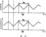
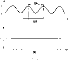
Shown in Figure 1 as 7 (1995)-No. 99795 communiques of Japanese kokai publication hei, in order to weaken noise component(s), the periodically variable power-converting device that will be used to produce the frequency of pulse width modulation carrier is used for Current Control.Yet, in this power-converting device, to carry out in the device of current sample, control calculating etc. with PWM generation cycle synchronisation, generation is according to the variation of the electric current computing cycle of the variation of carrier frequency (or cycle).For this reason, current controling characteristic is that weak point is long the variation according to carrier cycle.Therefore, shown in Figure 180 as explanation after a while is along with the change of output current wave takes place by the caused cyclical movement of the frequency change of pulse width modulation carrier (wherein, Tm represents cycle of changing).Generation is from the change of the output current wave of power-converting device, may cause the change (for example, the change of motor torque) by the running of the load that output drove of power-converting device.
Summary of the invention
Consider that above-mentioned problems of the prior art make the present invention.The purpose of this invention is to provide a kind of apparatus and method that are used to control power-converting device,, prevent that power-converting device from damaging its control characteristic even design these apparatus and method when power-converting device produces the frequency change of pulse width modulation carrier.
In order to solve foregoing problems, the invention provides a kind of control device that is used for power-converting device, thereby power-converting device produces alternating current output to carry out pulse-width modulation from the output of DC power supply, control device comprises: current controller, and it is transformed to voltage command value with given current command value; Carrier generator, it produces pulse width modulation carrier; The pulse-width modulation generator, it produces the signal after the pulse-width modulation that will supply to power-converting device according to voltage command value and pulse width modulation carrier; Frequency controller, it makes the frequency change from the pulse width modulation carrier of carrier generator; And the Current Control gain controller, its variation according to the frequency of pulse width modulation carrier makes the Current Control change in gain of current controller.In this control device, the Current Control of current controller gain basis changes from the variation of the frequency of the pulse width modulation carrier of carrier generator.According to the present invention, this control device is by producing the variation that is used for current command value is transformed to the Current Control gain of voltage command value according to the variation of PWM carrier frequency, suppress the generation of the cyclical movement that caused by the variation from the PWM carrier frequency of the output current wave of power-converting device.Thus, this control device is suppressed at the generation by the torque in the load of power-converting device driving and other change.
Incidentally, as will between PWM carrier frequency and Current Control gain, having fixing relation with reference to figure 8 explanations after a while.Because this relation can be by for example the linear approximation expression formula be given, so can use this expression formula to change the Current Control gain easily according to the variation of PWM carrier frequency.
About the indicial response to current command value, control device comprises the deviation detector of detection from the deviation of the output current of power-converting device and given current command value.Therefore, the control device basis is from the variation of the Current Control gain of the variation generation current controller of the PWM carrier frequency of carrier generator, the variation that also produces the scope of Current Control gain according to deviation.Thus, control device improves the transient characteristic from the output current wave of power-converting device.
Description of drawings
With reference now to description of drawings the present invention,, wherein:
Fig. 1 illustrates the block diagram that is used to control the device of power-converting device according to the first embodiment of the present invention;
Fig. 2 is the block diagram of current controller;
Fig. 3 is the block diagram of PWM generator;
Fig. 4 is the circuit diagram of power converter;
Fig. 5 is the flow chart that the computing of being carried out by frequency controller is shown;
Fig. 6 is the flow chart that the computing of being carried out by the Current Control gain controller is shown;
Fig. 7 is the performance plot that the relation between the side-play amount of Current Control gain and current value is shown;
Fig. 8 is the performance plot that the relation between carrier frequency and the Current Control gain is shown;
(a) of Fig. 9 and (b) be to be illustrated in that modulated carrier frequencies takes place so that sinusoidal waveform to be provided, Current Control gain curve chart with respect to the variation of time;
(a) of Figure 10 and (b) be to be illustrated in that modulated carrier frequencies takes place so that triangular waveform to be provided, Current Control gain curve chart with respect to the variation of time;
(a) of Figure 11 and (b) be take place when being illustrated in the carrier frequency change at random, Current Control gain is with respect to the curve chart of the variation of time;
Figure 12 is the block diagram that is used to control the device of power-converting device according to a second embodiment of the present invention;
Figure 13 is the block diagram that a third embodiment in accordance with the invention is used to control the device of power-converting device;
Figure 14 is the flow chart that the computing of being carried out by control device shown in Figure 13 is shown;
Figure 15 is the flow chart that the computing of a fourth embodiment in accordance with the invention is shown;
(a) of Figure 16 and (b) be that the curve chart of carrier frequency and Current Control gain with respect to the variation of time is shown respectively;
(a) of Figure 17 and (b) be to be illustrated in respectively under the situation of the present invention, carrier wave is with respect to the variation of time and motor phase current (phase current) figure with respect to the waveform of time;
(a) of Figure 18 and (b) be to be illustrated in respectively under the situation of comparative example, carrier wave is with respect to the variation of time and the motor phase current figure with respect to the waveform of time;
Figure 19 is the block diagram that the device that is used to control power-converting device according to a fifth embodiment of the invention is shown;
Figure 20 is the block diagram according to the current controller of the 5th embodiment;
(a) of Figure 21 is the performance plot that is illustrated in the relation between the side-play amount of proportional gain and current value under the transition state, and (b) of Figure 21 is the performance plot that is illustrated in the relation between the side-play amount of gain of transition state lower integral and current value;
(a) of Figure 22 is the performance plot that the relation between carrier frequency and the proportional gain is shown, and (b) of Figure 22 is the performance plot that the relation between carrier frequency and the storage gain is shown;
(a)~(d) of Figure 23 is carrier frequency fc, proportional gain Kp that current controller shown in Figure 20 is shown and the storage gain Ki figure with respect to the waveform of time;
Figure 24 is the block diagram that the device that is used to control power-converting device according to a sixth embodiment of the invention is shown;
(a)~(e) of Figure 25 is carrier frequency fc, proportional gain Kp, storage gain Ki and deviation that the control device shown in Figure 24 the is shown figure with respect to the waveform of time;
(a)~(c) of Figure 26 illustrates and is used for calculation flow chart and the mapping (map) controlled by control device shown in Figure 24;
Figure 27 is the block diagram that the device that is used to control power-converting device according to a seventh embodiment of the invention is shown; And
(a)~(d) of Figure 28 is the size (or absolute value) of carrier frequency fc, proportional gain Kp that the control device shown in Figure 27 is shown and deviation and the figure of the ratio of the size (or absolute value) of the variation of current command value.
Embodiment
Embodiments of the invention are described below with reference to the accompanying drawings, wherein represent identical member by identical Reference numeral.
First embodiment
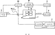
Fig. 1 is the block diagram of example that illustrates according to the power-converting device of the first embodiment of the present invention and be used to control the device of this power-converting device.
With reference to figure 1, power converter 2 for example is the PWM inverter that drives, thus load 3 (for example, motor) is provided alternating current by the pulse-width signal that comes self-controller 6 (hereafter is " pwm signal ").Current detector 4 detects the alternating current that flows to load 3 from power converter 2, and detected value is sent to controller 6.Current order generator 5 provides the command signal about the electric current that drives load 3.Current order generator 5 for example sends to controller 6 according to quantity of accelerator operation etc. with current command value when being installed to power-converting device on the vehicle.
To be elaborated to the piece shown in Fig. 1 below.
Fig. 2 is the block diagram that the structure of the current controller 7 in the controller 6 is shown.As shown in Figure 2, current controller 7 comprises: calculates from the detection current value of current detector 4 and calculator 71 from the deviation of the current command value of current order generator 5, and by carrying out the proportional controller 72 of proportional control (P-control) output voltage bid value.According to signal, the proportional of the proportional control that change used by proportional controller 72 is set, thereby the output voltage bid value changes according to the variation of carrier frequency from Current Control gain controller 10.Although provided the example of the proportional of proportional control as the Current Control gain of current controller 7 in Fig. 2, (for example, proportional-plus-integral is controlled, proportional-plus-integralcontrol) can to use other control system.
As used herein, obtain detection current value in the following manner from current detector 4.For example, current detector 4 detects the PWM inverters and offers U phase as the motor of load, V mutually and the W value of (or as provide as an example three-phase alternating current) electric current mutually here, and coordinate converter carry out conversion (or three-phase-two phase inversion) with U phase, V mutually and the W phase current values be transformed to the current value of d axial coordinate and q axial coordinate.
Fig. 3 is the block diagram that the structure of the PWM generator 8 in the controller 6 is shown.As shown in Figure 3, PWM generator 8 comprises: the coordinate converter 81 that the voltage command value by current controller 7 output is carried out coordinate transform, and the voltage command value after the coordinate transform and from the comparator 82 of the relative size of the carrier wave of carrier generator 9 relatively.
Fig. 4 is the circuit diagram that the structure of the power converter 2 shown in Fig. 1 is shown.As shown in Figure 4, power converter 2 comprises: DC power supply 21, capacitor 22 and 6 switch elements 23 (being used for three-phase alternating current).In the switch element 23 each is made of the semiconductor device of for example igbt (IGBT, insulated gate bipolar transistor).Switch element 23 bases are from the pwm signal (Vu of the comparator 82 of PWM generator 8
+, Vu
-, Vv
+, Vv
-, Vw
+, Vw
-) select the positive electrode or the negative electrode of the DC power supply that forms by DC power supply 21 and capacitor 22, selected electrode is to U phase, V phase or the W phase electrode power supply of load 3 (or motor).
The value of the U phase that current detector 4 detection power converters 2 (or PWM inverter) provide to load 3 (or motor), V phase and W phase current.
In addition, the frequency controller shown in Fig. 1 11 variation that produces carrier frequency according to timing from the peak (or maximum) of the input triangular wave of carrier generator 9 or paddy (or minimum value).In this case, will describe as example with the situation that the triangular wave form is provided as carrier wave and modulated carrier frequencies to use triangular wave.
Have under the situation of the power-converting device of structure as mentioned above, frequency controller 11 execution graphs 5 and FREQUENCY CONTROL shown in Figure 6 are handled, and can prevent the generation of the fault that the variation owing to carrier frequency causes thus, and do not damage the efficient of motor.
At first, will how to move to carry out FREQUENCY CONTROL frequency controller 11 with reference to flow chart shown in Figure 5 and handle and be described in detail.
At first at step S0, frequency controller 11 is determined higher limit fmax and the lower limit fmin of the carrier frequency f that will be changed by frequency controller 11, to with the frequency band division between fmax and the fmin value what grades (step), and the changing value Δ (Δ=(fmax-fmin)/number of degrees).Next this treatment step carries out step S1 to import triangular wave carriers from carrier generator 9 to frequency controller 11.
At step S1, frequency controller 11 judges whether the incoming carrier from carrier generator 9 has maximum or minimum value, that is, whether the carrier signal value equals peak value.When frequency controller 11 is judged as carrier wave when equaling maximum or minimum value, then control and treatment proceeds to step S2.
At step S2, frequency controller 11 judges that the changing value Δ of carrier frequency f is just or negative.When the changing value Δ when negative, control and treatment proceeds to step S5.When the changing value Δ is timing, control and treatment proceeds to step S3.
At step S3, whether frequency controller 11 determination frequency f reach higher limit fmax.When making frequency f and do not reach the judgement of higher limit fmax, control and treatment proceeds to step S7, makes the symbol of changing value Δ not change.When frequency f reached higher limit fmax, control and treatment proceeded to step S4.
At step S4, the symbol of the changing value Δ of frequency controller 11 reversal frequency f (Δ ←-Δ), thereby next time and reduce frequency f during calculating thereafter.This makes step S4 finish, and control and treatment proceeds to step S7 from step S 4.
At step S5, whether frequency controller 11 determination frequency f reach lower limit fmin.When making frequency f and do not reach the judgement of lower limit fmin, control and treatment proceeds to step S7, makes the symbol of changing value Δ not change.When frequency f reached lower limit fmin, control and treatment proceeded to step S6.
At step S6, the symbol of the changing value Δ of frequency controller 11 reversal frequency f, thereby next time and increase frequency f during calculating thereafter.This makes step S6 finish, and control and treatment proceeds to step S7 from step S6.
At step S7, frequency controller 11 will be added to the carrier frequency f that is input to the next cycle of carrier generator 9 on the current frequency f with the calculating meeting in order by the changing value Δ that above treatment step is determined.In other words, thus control frequency f carries out monotone increasing with the changing value Δ at every turn when calculating add deduct little.This makes step S7 finish, and FREQUENCY CONTROL is handled and turned back to step S1 from step S7.
Above-mentioned a series of FREQUENCY CONTROL is handled step and is made and reduce and increase in that next time period intercarrier frequency f is dull in given time period intercarrier frequency f dullness,, carrier frequency f is modulated to the form of triangular wave that is.
Fig. 6 is the flow chart that is illustrated in the computing that takes place in the Current Control gain controller 10.
Except higher limit Kpmax, the lower limit Kpmin of Current Control gain Kp and higher limit fmax, lower limit fmin and changing value Δ that changing value Δ Kp replaces frequency f respectively, the processing of the Fig. 6 that is undertaken by Current Control gain controller 10 is identical with the processing of top Fig. 5.The step S0 ' of Fig. 6, S1 ', S2 '~S7 ' are corresponding with step S0~S7 of Fig. 5 respectively.In other words, Control current ride gain Kp adds deduct little thereby carry out monotone increasing with changing value Δ Kp when each calculating takes place.
The feasible Current Control gain Kp that can change current controller 7 with the form of triangular wave of the processing of execution graph 6 according to the variation of carrier frequency f.
With reference now to Fig. 7, the higher limit Kpmax and the lower limit Kpmin of the gain of the Current Control shown in Fig. 6 are described.
Fig. 7 illustrates the variation of the deviation that is caused by carrier frequency.In Fig. 7, transverse axis is represented the Current Control gain of the current controller 7 when the input of fixing current command value is provided, and the longitudinal axis is represented current command value and detected difference (that is, side-play amount or deviation) between the current value.
From Fig. 7 as seen, when the Current Control gain setting is fixed value,, carrier frequency f becomes big along with uprising (or approaching higher limit fmax) deviation, and along with carrier frequency f step-down (or approaching lower limit fmin) deviation diminishes.This shows: when the Control current ride gain, its increase with carrier frequency f is increased or with carrier frequency f reduce and when reducing, deviation can be maintained fixed.Incidentally, because the inverse of frequency is the cycle when setting carrier frequency based on the cycle, so thereby the control of next stage is equal to be set the Current Control gain and it is reduced along with the growth of carrier cycle or increase along with the shortening of carrier cycle.
Experiment shows to exist goes up relation of plane,, has the given rule relation that deviation can be maintained fixed between carrier frequency and Current Control gain that is.Fig. 8 illustrates the figure that concerns above.In Fig. 8, the longitudinal axis is represented the Current Control gain, and transverse axis is represented carrier frequency.From Fig. 8 as seen, carrier frequency basically with the Current Control linear ratio that gains.
Although can make the corresponding Current Control gain of Current Control gain to determine to make deviation fixing with the carrier frequency (or cycle) of all changes, but can use the linear approximation expression formula that obtains from the relation shown in Fig. 8, determine the Current Control gain according to the higher limit and the lower limit of Current Control gain.When the higher limit of having determined carrier frequency (or cycle) according to Fig. 8 and lower limit, therefore can will the higher limit fmax of the fixing carrier frequency (or cycle) of deviation and the corresponding higher limit Kpmax and the lower limit Kpmin combination of lower limit fmin and Current Control gain be provided with.
(b) of (a)~Figure 11 of Fig. 9 be illustrated in take place when using above-mentioned control method, carrier frequency (or cycle) and Current Control gain with respect to the variation of time.(a) of Fig. 9 and (b) be the curve chart that is illustrated in the variation of the Current Control gain that modulated carrier frequencies takes place so that sinusoidal waveform to be provided.(a) of Figure 10 and (b) be the curve chart that is illustrated in the variation of the Current Control gain that modulated carrier frequencies takes place so that triangular waveform to be provided.(a) of Figure 11 and (b) be the Current Control gain that takes place when being illustrated in the carrier frequency change at random curve chart with respect to the variation of time.(a) of (a) of Fig. 9, (a) of Figure 10 and Figure 11 illustrates carrier frequency with respect to the variation of time, and (b) of (b) of Fig. 9, (b) of Figure 10 and Figure 11 illustrates the variation of Current Control gain with respect to the time.In these figure, Tm represents cycle of changing.
As mentioned above,, change the Current Control gain, so the Current Control gain is also along with the variation one of carrier frequency changes according to the variation of carrier frequency.This makes and can suppress because the change from the output current of power-converting device that the variation of carrier frequency causes.
In addition, proportional control is used for current controller 7.Thereby, can realize the simple control of Current Control gain by the proportional that changes proportional control.
In addition, can modulated carrier frequencies so that the triangular wave form to be provided.This is convenient to calculate and setpoint frequency and Current Control gain, thereby can suppress the change from the output current of power-converting device.
Second embodiment
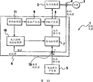
Figure 12 is the block diagram that the device that is used to control power-converting device according to a second embodiment of the present invention is shown.
Control device according to second embodiment is set with the mapping 12 of storing the correlation between carrier frequency and the Current Control gain, the frequency controller 11 shown in the alternate figures 1.Use is controlled from shining upon 12 values of reading, so that carrier generator 9 produces variable frequency.In addition, the value from mapping 12 is used to make Current Control gain controller 10 to change the Current Control gain of current controller 7 according to the variation of carrier frequency.This can prevent effectively because the generation of the fault that the variation of carrier frequency causes.The structure of other assembly is identical with the structure shown in previous described Fig. 1.
As mentioned above, carrier frequency and Current Control gain mapping mutually change carrier frequency and Current Control gain according to this mapping.This has reached the effect of Combination of being convenient to be provided with complicated carrier frequency and Current Control gain.
The 3rd embodiment
Figure 13 illustrates the block diagram that a third embodiment in accordance with the invention is used to control the device of power-converting device.
Control device according to the 3rd embodiment is set with the periodically variable periodic frequency controller 13 that produces frequency, has substituted the frequency controller 11 shown in Fig. 1.
Figure 14 illustrates the flow chart that is used for the method for Control current ride gain according to the 3rd embodiment.
The flow chart of Figure 14 is being combined to form by the flow chart of earlier figures 5 and Fig. 6.The step S0 of Figure 14 " comprise that the step S0 of execution graph 5 adds the gain initialization shown in Fig. 6 (or step S0 ' of Fig. 6).Step S4 ", S6 " and S7 " comprise and step S4 ', the S6 ' of Fig. 6, change step S4, S6, the change of carrier frequency f among the S7 of execution graph 5 simultaneously of Current Control gain Kp among the S7 '.In this case, carrier frequency can be changed the arbitrary form into for example curve form, unless that the variable quantity of carrier frequency becomes is very big.
Incidentally, by result calculated shown in Figure 14 is stored in the mapping, can generate the mapping 12 shown in Figure 12.
As mentioned above, the cyclic variation of carrier frequency is convenient to calculate and estimating carrier frequency, thereby can change the Current Control gain according to the variation of carrier frequency, therefore can suppress the change from the output current of power-converting device.
The 4th embodiment
Figure 15 is the flow chart of the control method of the aid illustration a fourth embodiment in accordance with the invention device that is used to control power-converting device.
Be used for according to the control method of the 4th embodiment that the delay according to carrier wave postpones and changes Current Control to gain when carrier wave taking place postpone.
Under the situation of control device shown in Figure 11, the carrier wave that supplies to PWM generator 8 from carrier generator 9 may be owing to being buffered or postpone computing time.Under the situation of this structure, carry out step S7 with Figure 14 " corresponding treatment step (or step S7 and S8 of Figure 15).More specifically, the changing value Δ Kp with the Current Control gain when calculating end remains Δ Kp1 (at the step S8 of Figure 15) temporarily, will be worth Δ Kp1 and be used for calculating (at the step S7 of Figure 15 ) next time.In other words, compare with computing shown in Figure 14, processing shown in Figure 15 is used for having postponed by use the value of Current Control gain of the duration of a computation cycles and comes the calculating voltage bid value.More specifically, when the PWM carrier wave of the PWM generator 8 that supplies to power-converting device from carrier generator 9, taking place to postpone, the duration that will keep a computation cycles by the Current Control yield value that the order of sending to current controller 7 from Current Control gain controller 10 is indicated, thus use the Current Control yield value that is kept so that current controller 7 calculating voltage bid values to calculate next time.Thereby carry out this operation and can change the Current Control gain, make to prevent effectively because the fault that the delay in calculating etc. are produced by carrier frequency according to the variation of carrier frequency.
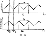
(a) of Figure 16 and (b) carrier frequency that produced by above-mentioned processing and the variation of Current Control gain be shown respectively.At (a) of Figure 16 with (b), D represents to equal the delay of the duration of a computation cycles.
Although above provided the Current Control gain is kept the example of the duration of a computation cycles, also can the Current Control gain be kept the duration of repeatedly calculating according to the delay degree of carrier wave.
Now for variation, and describe when the gain variation of variation according to the carrier frequency motor phase current of (or under situation of the present invention) generation when changing of Current Control when the Current Control gain motor phase current that (or under the situation at comparative example) takes place fixedly the time.
(a) of Figure 17 and (b) and Figure 18 (a) and (b) be the figure of characteristic that the variation of the carrier frequency that presents when with the sine wave modulation carrier frequency and electric current is shown.(a) of Figure 17 and the characteristic that (b) the present invention is shown is had, (a) of Figure 18 and the characteristic that (b) comparative example is shown is had.
(a) of Figure 17 and (a) of Figure 18 illustrate the variation of carrier frequency with respect to the time.In Figure 17 (a) and Figure 18 (a), Tm represents the period of change with respect to the time.(b) of Figure 17 illustrates (or under situation of the present invention) forms when Current Control gain changes according to the variation of carrier frequency the motor phase current waveform with respect to the time.The motor phase current that (or under situation of comparative example) formed when the Current Control that illustrates (b) of Figure 18 gained fixedly is with respect to the waveform of time.
From (a)~Figure 18 of Figure 17 (b) as seen, as what observed under the situation of comparative example, the motor phase current changes according to the change of carrier frequency, and as under situation of the present invention, observing, even carrier frequency cyclical movement, motor phase current also almost keep stable with the straight line waveform.In view of the above, visible method of the present invention suppresses the change of electric current.
To carrier frequency being modulated to the triangular wave form or carrying out identical processing with the situation of random fashion modulated carrier frequencies.More specifically, compare with fixing Current Control gain, the Current Control gain that changes according to the variation of carrier frequency can suppress the change of motor phase current, therefore can prevent the generation by the caused fault of carrier frequency effectively.
The 5th embodiment
With reference to aforementioned first to the 4th embodiment, provided following example: the stable state of current command value basic fixed wherein occurred, and had the single deviation of output current and current command value.The 5th embodiment is suitable for satisfying following situation: the current command value change wherein occurred and had the transition state of the change deviation (that is, exist a plurality of deviations and change separately) of a plurality of output currents and current command value.
Figure 19 is the block diagram that the device that is used to control power-converting device according to a fifth embodiment of the invention is shown.In Figure 19, represent essentially identical part by identical Reference numeral shown in Figure 1.Below the structure different with structure shown in Fig. 1 described.
Outside current controller 7, be provided with the deviation detector 70 of the deviation that is used to detection current value and current command value according to the control device of the 5th embodiment.By this structure, according to detected Deviation Control Current Control gain controller 10, thereby change the Current Control gain of current controller 7 according to the variation of carrier frequency, also change the scope (for example, the mean value of the band of Current Control change in gain) of Current Control gain according to deviation.In other words, because in the transition state of current command value change, there are a plurality of change deviations of output current and current command value, so this control device is used for changing according to the variation of deviation the scope of Current Control gain.This can realize the improvement from the transient characteristic of the output current wave of power-converting device.
Be elaborated below.
Figure 20 is the block diagram that the structure of the current controller 7 in the controller 6 is shown.As shown in Figure 20, deviation detector 70 detects from the detection current value of current detector 4 and deviation from the current command value of current order generator 5.Incidentally, obtain detection current value in the following manner from current detector 4.For example, current detector 4 detects the value that power converter 2 (or PWM inverter) offers U phase, V phase and W phase current (or three-phase alternating current as an example) as the motor of load 3, and coordinate converter carries out conversion (or three-phase-binomial conversion) so that U phase, V phase and W phase current values are transformed to d axial coordinate and q axial coordinate current value.
Current Control gain controller 10 bases are gone back the variation (will describe in detail after a while) of the scope that gains according to the deviation generation Current Control from deviation detector 70 from the variation of the Current Control gain of the variation generation current controller 7 of the carrier frequency of frequency controller 11.
(a) of Figure 21 and (b) be the figure of the method for the aid illustration Current Control gain (or proportional gain and storage gain) that is used for Control current controller 7, it illustrates the variation of the deviation that is caused by predetermined carrier frequency.In (a) of Figure 21, transverse axis is represented the proportional gain Kp of current controller 7 when the input of the current command value that change is provided, and the longitudinal axis is represented the difference (that is, side-play amount or deviation) between current command value and the detection current value.In (b) of Figure 21, transverse axis is represented the storage gain Ki of current controller 7 when the input of the current command value that change is provided, and the longitudinal axis is represented the difference (that is, side-play amount or deviation) between current command value and the detection current value.At (a) of Figure 21 with (b), fcmax and fcmin represent higher limit and the lower limit corresponding characteristic curve with carrier frequency respectively.
Under transition state, deviation also changes along with the variation of current command value.By predetermined reference value e1, e2 and e3 the size of deviation is divided into 4 parts.When the deviation e value of being equal to or greater than e1 (e 〉=e1), the scope of gain Kp is made as 1}, and gain Kp in scope { 1} in the carrier synchronization variation.When being positioned between value e2 (comprising) and the value e1 (not comprising), deviation e (during e1>e 〉=e2), the scope of gain Kp is made as { 2}, and gain Kp is in scope { variation 2} in.Similarly, (during e2>e 〉=e3), gain Kp { change with carrier synchronization 3} in, or (during e3>e), gain Kp is in scope { in the 4} and the carrier synchronization variation less than value e3 as deviation e in scope when deviation e is positioned between value e3 (comprising) and the value e2 (not comprising).The situation of the excursion of Ki and proportional gain Kp is similarly determined.
In other words, the scope of gain Kp and Ki changes according to the size of deviation e.In (a) of Figure 21, the scope of gain Kp is set according to the mean value of the mean value of the higher limit (corresponding to curve fcmax) of the Current Control of each deviation region of dividing gain and lower limit (corresponding to curve fcmin) thereof.For example, when deviation e is positioned between value e2 (comprising) and the value e1 (not comprising) (during e1>e 〉=e2), with the mean value of the corresponding gain Kp from value e1 to the curve fcmax of value e2 scope be scope the higher limit of 2}, and with the corresponding mean value that gains Kp of curve fcmin of scope from value e1 to value e2 be the scope { lower limit of 2}.
Incidentally, be not limited to by size and the definite mean value of dividing deviation scope is set as described above, also can scope be set corresponding to each deviation.
Figure 22 (a) illustrates the figure that concerns between carrier frequency and the proportional gain.Figure 22 (b) illustrates the figure that concerns between carrier frequency and the storage gain.At (a) of Figure 22 with (b), the longitudinal axis is represented the Current Control gain, and transverse axis is represented carrier frequency.From (a) of Figure 22 and (b) as seen, all linear basically ratio of carrier frequency and proportional gain and storage gain.
Although can make proportional gain or storage gain corresponding with the frequency (or cycle) of the carrier wave that all changes, with proportional gain or the storage gain of determining to make deviation fixing, but can use according to (a) of Figure 22 and linear approximation expression formula that the relation (b) obtains, determine proportional gain or storage gain according to the higher limit and the lower limit of proportional gain or storage gain.As the scope of having determined proportional gain or storage gain as previously mentioned { 1}~{ when 4} and higher limit and lower limit, therefore can will make the higher limit fcmax of the carrier frequency (or cycle) that deviation is fixing and the corresponding higher limit Kpmax of lower limit fcmin and proportional gain and the Kimax and the Kimin combination of following restriction Kpmin or storage gain be provided with.
(a)~(d) of Figure 23 illustrates carrier frequency fc that (a)~Figure 22 by using Figure 21 (b) be provided with and proportional gain Kp and the storage gain Ki figure with respect to the waveform of time.(a) of Figure 23 illustrates in response to the output current of the current command value ref waveform with respect to the time.(b) of Figure 23 illustrates the variation with respect to the time from the carrier frequency fc of carrier generator 9.The variation of the proportional gain Kp of current controller 7 when (c) of Figure 23 is illustrated in the input that current command value ref is provided.The variation of the storage gain Ki of current controller 7 when (d) of Figure 23 is illustrated in the input that current command value ref is provided.
In (a) of Figure 23, the difference between dotted line (being current command value ref) and the solid line (promptly detecting current value) is corresponding to deviation.In (a) of Figure 23, e1, e2 and e3 represent the above-mentioned fiducial value that is used to divide the size of deviation.Carrier frequency fc shown in proportional gain Kp shown in Figure 23 (c) and Figure 23 (b) changes synchronously with respect to the variation of time, in addition, the gain Kp scope according to deviation shown in Figure 23 (a) from { 1} changes to { 4}.
Although Figure 23 (a)~(d) provided by fiducial value e1, e2 and e3 and divided the example of the size of deviation, the quantity of zoning is not limited to this example.
Said structure can change the scope of Current Control gain according to the deviation of output current and current command value.
Except recited above, can also with reference to the content application of first to the 4th embodiment explanation in the 5th embodiment.More specifically, these contents comprise following configuration: when frequency controller produces the cyclic variation of carrier frequency maybe when taking place to postpone the voltage command value that supplies to the PWM generator from current controller, the Current Control yield value that will be provided by the order from the Current Control gain controller keeps carrying out predetermined quantity and calculates the required duration, and current controller uses the Current Control yield value that is kept to come the calculating voltage bid value to calculate next time.
The 6th embodiment
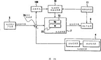
Figure 24 is the block diagram that the device that is used to control power-converting device according to a sixth embodiment of the invention is shown.In Figure 24, represent identical part by Reference numeral identical shown in Figure 20.
By control device, and additionally be used to judge that the judging unit 100 of the size of deviation constitutes according to the control device of the 6th embodiment according to the 5th embodiment.
(a)~(e) below with reference to Figure 25 describes for the operation of judging unit 100 and the method for definite gain Kp.
That (a) of Figure 25 illustrates is that current command value forms when ref1 changes to ref2, in response to the output of current command value waveform with respect to the time.(b) of Figure 25 illustrates size under the situation, deviation (or absolute value) shown in (a) that occurs in Figure 25 with respect to the variation of time.(c) of Figure 25 illustrates the variation of carrier frequency.(d) of Figure 25 illustrates the variation of the gain Kp under the situation shown in (c) that occurs in Figure 25.(e) of Figure 25 illustrates the variation of the gain Ki under the situation shown in (c) that occurs in Figure 25.
Shown in for example Figure 25 (b), during fiducial value that value e1 is judged as judging unit 100, if the absolute value value of being equal to or greater than e1 of deviation, the scope of the Kp that then gains is set to { 2}; If perhaps the absolute value of deviation is less than value e1, the scope of the Kp that then gains is set to { 1}.This can reduce the toning (overshoot) under the transition state, thereby improves the controllability under the transition state.
Although provided the forward position of current command value as an example in (a)~(e) of Figure 25, the 6th embodiment can also have identical effect to the back edge of current command value.
(a)~(c) of Figure 26 is illustrated in calculation flow chart and the mapping of using in the control with reference to Figure 25 (a)~(e) explanation.
At first, shown in Figure 26 (c), the PWM carrier frequency of change is set to fc (1)~fc (n).In (c) of Figure 26, fc (1)~fc (n) is expressed as fc1~fcn respectively.
Then, shown in Figure 26 (b), generate fc-Kp, Ki (carrier frequency-gain) mapping.Value in the mapping can be used for controlling to produce the synchronous variation of carrier frequency fc and gain Kp, Ki.
In Figure 26 (b) { part that 1}Kp row are included in gain Kp shown in (a) of Figure 21 { makes the combination of the fixing carrier frequency fc of deviation and the Kp that gains according to the quantity of the carrier frequency fc that is divided the scope (between fcmin and the fcmax) of carrier frequency among the 1}.In other words, the gain Kp part { among the 1}, { 1}Kp (1)~{ 1}Kp (n) corresponds respectively to carrier frequency fc (1)~fc (n) to scope, and has the deviation of making fixed K p value.With { situation of 1}Kp row is identical, { part that 2}Kp is listed as the Kp of gain shown in (a) that is included in Figure 21 { among the 2}, makes the combination of fixing carrier frequency fc of deviation and gain Kp according to the quantity of the carrier frequency fc that is divided in the scope (between fcmin and the fcmax) of carrier frequency.
Provide explanation now for computing shown in Figure 26 (a).When calculating beginning, at first the value m of counter is set to 1.At step S10, carrier frequency is set to fc (1).At step S11, the value of calculation deviation e.At step S12, the value of deviation e is compared with fiducial value e1.When the absolute value of deviation e during, handle proceeding to step S13 less than fiducial value e1.At step S13, { value of 1}Kp (1) is set to the gain Kp of the current controller 7 shown in Figure 24, and { value of 1}Ki (1) is set to the gain Ki of current controller 7, handles proceeding to step S15 then.At step S15, the value m of counter is counting upwards.At step S16, the value m of counter and the value of n are compared.As the value m of counter during less than the value of n, handle and turn back to step S11, repeat top calculating then.When the relatively demonstration deviation e at step S12 is equal to or greater than fiducial value e1, handle proceeding to step S14.At step S14, { value of 2}Kp (2) is set to the Kp that gains, and { value of 2}Ki (2) is set to the Ki that gains, and handles proceeding to step S15 then.
Control shown in Figure 25 (a)~(d) can be realized by above-mentioned processing.
The 7th embodiment
Figure 27 is the block diagram that the device that is used to control power-converting device according to a seventh embodiment of the invention is shown.In Figure 27, represent identical part by Reference numeral identical shown in Figure 20.
By the control device according to the 5th embodiment, and the judging unit 101 of the additional size that is used to judge deviation (or absolute value) that is provided with and the ratio of the size (or absolute value) of the variation of current command value constitutes according to the control device of the 7th embodiment.
(a)~(d) below with reference to Figure 28 describes for the operation of judging unit 101 and the method for definite gain Kp.
That (a) of Figure 28 illustrates is that current command value forms when ref1 changes to ref2, in response to the output of current command value waveform with respect to the time.(b) of Figure 28 is illustrated in the variation of the ratio of size that take place, deviation (or absolute value) and the amount (or absolute value) of the variation of current command value under the situation shown in (a) of Figure 28 with respect to the time.(c) of Figure 28 illustrates the variation of carrier frequency.(d) of Figure 28 is illustrated in the variation of the gain Kp that takes place under the situation shown in (c) of Figure 28.
For example shown in Figure 28 (b), when e1 on duty judges as the fiducial value of judging unit 101, if the ratio value of being equal to or less than e1 of the amount of the variation of the size of deviation and current command value, the scope of Kp of then gaining is set to { 2}, if perhaps the ratio of the amount of the variation of the size of deviation and current command value is greater than value e1, the scope of the Kp that then gains is set to { 1}.This can reduce the toning under the transition state, thereby improves the controllability under the transition state.
Although provided the forward position of current command value as an example in (a)~(d) of Figure 28, the 7th embodiment can also have identical influence to the back edge of current command value.In addition, use the ratio of size (or absolute value) with the amount (or absolute value) of the variation of current command value of deviation, thereby the fiducial value e1 that can be used to judge is set to the percentage (%) of amount of the variation of current command value.
When for eliminate by pwm signal open or close power-converting device the high order harmonic component that switch element produced switching noise and when changing the PWM carrier frequency, the cyclical movement that the variation by the PWM carrier frequency causes takes place in from the output current wave of power-converting device.According to the foregoing description, produce the variation that current command value is transformed to the Current Control gain of voltage command value by the variation according to the PWM carrier frequency, control device and method can suppress the generation from the caused cyclical movement of variation of the PWM carrier frequency of the output current wave of power-converting device.Therefore, control device and method have realized eliminating the effect of the faults such as moment of torsion change that take place in the load that is driven by power-converting device.Indicial response for current command value, control device and method can produce the variation of the Current Control gain of current controller according to the variation from the PWM carrier frequency of carrier generator, the variation that can also produce the scope of Current Control gain according to the deviation from the output current of power-converting device and given current command value.Therefore, control device and method have realized improving the effect from the transient characteristic of the output current wave of power-converting device.
Here Shuo Ming preferred embodiment only is exemplary and not restrictive, and the present invention can otherwise realize or implement, and does not break away from its essence or essential characteristic.Scope of the present invention is specified by claims, and hope is contained in this with the whole variations in claims.
The disclosure relates to Japanese patent application 2006-122093 number and the theme in Japanese patent application 2007-31587 number of submission on February 13rd, 2007 that is included in submission on April 26th, 2006, and it all is contained in this by reference.
Claims (16)
1. control device that is used for power-converting device, thus described power-converting device produces alternating current output to carry out pulse-width modulation from the output of DC power supply, and described control device comprises:
Current controller, it is transformed to voltage command value with given current command value;
Carrier generator, it produces pulse width modulation carrier;
The pulse-width modulation generator, it produces the signal after the pulse-width modulation that will supply to described power-converting device according to described voltage command value and described pulse width modulation carrier;
Frequency controller, it makes the frequency change from the described pulse width modulation carrier of described carrier generator; And
The Current Control gain controller, its variation according to the frequency of described pulse width modulation carrier makes the Current Control change in gain of described current controller,
Wherein, the described Current Control gain basis of described current controller changes from the variation of the frequency of the described pulse width modulation carrier of described carrier generator.
2. the control device that is used for power-converting device according to claim 1 is characterized in that described current controller is a proportional controller, changes described Current Control gain by the proportional that changes described proportional controller.
3. the control device that is used for power-converting device according to claim 1 is characterized in that, described frequency controller changes the frequency period ground of described pulse width modulation carrier.
4. the control device that is used for power-converting device according to claim 1, it is characterized in that, when taking place to postpone the described voltage command value that supplies to described pulse-width modulation generator from described current controller, will be by keeping carrying out the duration that predetermined quantity calculates from the given Current Control yield value of the order of described Current Control gain controller, and described current controller uses the Current Control yield value that is kept to calculate described voltage command value to calculate next time.
5. control method that is used for power-converting device, thus described power-converting device produces alternating current output to carry out pulse-width modulation from the output of DC power supply, and described control method comprises:
Given current command value is transformed to voltage command value;
Produce the signal after the pulse-width modulation that will supply to described power-converting device according to described voltage command value and pulse width modulation carrier;
Make the frequency change of described pulse width modulation carrier; And
Variation according to the frequency of described pulse width modulation carrier is used in the Current Control change in gain that described current command value is transformed to described voltage command value.
6. the control method that is used for power-converting device according to claim 5, it is characterized in that, proportional control is used for given current command value is transformed to the calculating of described voltage command value, changes described Current Control gain by the proportional that changes described proportional control.
7. the control method that is used for power-converting device according to claim 5 is characterized in that, the frequency of the described pulse width modulation carrier of periodic variation.
8. the control method that is used for power-converting device according to claim 5, it is characterized in that, when in described pulse width modulation carrier, taking place to postpone, the value of described Current Control gain is kept carrying out duration of the calculating of predetermined quantity, and use the Current Control yield value that is kept to calculate described voltage command value calculate next time.
9. control device that is used for power-converting device, thus described power-converting device produces alternating current output to carry out pulse-width modulation from the output of DC power supply, and described control device comprises:
Current controller, it is transformed to voltage command value with given current command value;
Carrier generator, it produces pulse width modulation carrier;
The pulse-width modulation generator, it produces the signal after the pulse-width modulation that will supply to described power-converting device according to described voltage command value and described pulse width modulation carrier;
Frequency controller, it makes the frequency change from the described pulse width modulation carrier of described carrier generator;
The Current Control gain controller, its variation according to the frequency of described pulse width modulation carrier makes the Current Control change in gain of described current controller; And
Deviation detector, it detects the deviation from the output current of described power-converting device and described given current command value,
Wherein, the described Current Control gain basis of described current controller changes from the variation of the frequency of the described pulse width modulation carrier of described carrier generator, and the scope of described Current Control gain changes according to described deviation.
10. the control device that is used for power-converting device according to claim 9, it is characterized in that, the size of described deviation is divided into a plurality of parts, and sets the scope of described Current Control gain according to the mean value of the lower limit of the mean value of the higher limit of Current Control described in each part gain and the gain of described Current Control.
11. the control device that is used for power-converting device according to claim 9 is characterized in that, also comprises the absolute value that is used to judge described deviation whether greater than the judging unit of pre-determined reference value,
Wherein, when the absolute value of described deviation during, the scope of described Current Control gain is set at different when absolute value when described deviation is equal to or less than described fiducial value greater than described fiducial value.
12. the control device that is used for power-converting device according to claim 9, it is characterized in that, whether the ratio of absolute value of size of variation that also comprises the absolute value of the size of judging described deviation and described current command value is greater than the judging unit of pre-determined reference value
Wherein, when the ratio of the absolute value of the size of the variation of the absolute value of the size of described deviation and described current command value during, the scope of described Current Control gain is set at different with when described ratio is equal to or less than described fiducial value greater than described fiducial value.
13. a control method that is used for power-converting device, thus described power-converting device produces alternating current output to carry out pulse-width modulation from the output of DC power supply, and described control method comprises:
Given current command value is transformed to voltage command value;
Produce the signal after the pulse-width modulation that will supply to described power-converting device according to described voltage command value and pulse width modulation carrier;
Make the frequency change of described pulse width modulation carrier;
Detection is from the deviation of the output current of described power-converting device and described given current command value; And
Variation according to the frequency of described pulse width modulation carrier is used in the Current Control change in gain that described current command value is transformed to described voltage command value, and the scope of described Current Control gain changes according to described deviation.
14. the control method that is used for power-converting device according to claim 13, it is characterized in that, the size of described deviation is divided into a plurality of parts, and sets the scope of described Current Control gain according to the mean value of the lower limit of the mean value of the higher limit of Current Control described in each part gain and the gain of described Current Control.
15. the control method that is used for power-converting device according to claim 13 is characterized in that, whether also comprises the absolute value of judging described deviation greater than pre-determined reference value,
Wherein, when the absolute value of described deviation during, the scope of described Current Control gain is set at different when absolute value when described deviation is equal to or less than described fiducial value greater than described fiducial value.
16. the control method that is used for power-converting device according to claim 13 is characterized in that, whether the ratio of absolute value of size of variation that also comprises the absolute value of the size of judging described deviation and described current command value greater than pre-determined reference value,
Wherein, when the ratio of the absolute value of the size of the variation of the absolute value of the size of described deviation and described current command value during, the scope of described Current Control gain is set at different with when described ratio is equal to or less than described fiducial value greater than described fiducial value.
Applications Claiming Priority (6)
| Application Number | Priority Date | Filing Date | Title |
|---|---|---|---|
| JP2006122093 | 2006-04-26 | ||
| JP2006122093 | 2006-04-26 | ||
| JP2006-122093 | 2006-04-26 | ||
| JP2007031584 | 2007-02-13 | ||
| JP2007031584 | 2007-02-13 | ||
| JP2007-031584 | 2007-02-13 |
Publications (2)
| Publication Number | Publication Date |
|---|---|
| CN101064483A true CN101064483A (en) | 2007-10-31 |
| CN101064483B CN101064483B (en) | 2011-02-02 |
Family
ID=38353392
Family Applications (1)
| Application Number | Title | Priority Date | Filing Date |
|---|---|---|---|
| CN2007100980495A Expired - Fee Related CN101064483B (en) | 2006-04-26 | 2007-04-26 | Device and method for controlling power converting device |
Country Status (4)
| Country | Link |
|---|---|
| US (1) | US7639518B2 (en) |
| EP (1) | EP1850465B1 (en) |
| JP (1) | JP5023788B2 (en) |
| CN (1) | CN101064483B (en) |
Cited By (12)
| Publication number | Priority date | Publication date | Assignee | Title |
|---|---|---|---|---|
| CN101919151A (en) * | 2008-01-18 | 2010-12-15 | 三菱电机株式会社 | Controller of power converter |
| CN102893510A (en) * | 2010-06-03 | 2013-01-23 | 日产自动车株式会社 | Electric motor controller and electric motor control system |
| CN102934355A (en) * | 2010-06-07 | 2013-02-13 | 丰田自动车株式会社 | Control method and control device for an electric power regulator |
| CN104242756A (en) * | 2013-06-19 | 2014-12-24 | 富士电机株式会社 | Stepping motor drive device |
| CN105553381A (en) * | 2014-10-22 | 2016-05-04 | 精工爱普生株式会社 | Robot |
| CN106464154A (en) * | 2014-06-18 | 2017-02-22 | 株式会社日立制作所 | Inverter and drive system using same |
| CN106797189A (en) * | 2014-08-29 | 2017-05-31 | 日产自动车株式会社 | Variable magnetization machine controller |
| CN107425784A (en) * | 2016-04-28 | 2017-12-01 | 丰田自动车株式会社 | Vehicle |
| CN107800350A (en) * | 2017-10-23 | 2018-03-13 | 广东美的制冷设备有限公司 | Speed-adjusting circuit of alternating and air conditioner |
| CN108539993A (en) * | 2018-04-26 | 2018-09-14 | 广东美的厨房电器制造有限公司 | Control method, electronic transformer and the microwave cooking electric appliance of electronic transformer |
| CN111201701A (en) * | 2017-10-17 | 2020-05-26 | 日立汽车系统株式会社 | Control device |
| CN114594704A (en) * | 2020-12-07 | 2022-06-07 | 山东新松工业软件研究院股份有限公司 | Motor inner ring control method, device and controller |
Families Citing this family (30)
| Publication number | Priority date | Publication date | Assignee | Title |
|---|---|---|---|---|
| US7649756B2 (en) * | 2006-05-17 | 2010-01-19 | Rockwell Automation Technologies, Inc. | Common mode noise reduction in converter systems through modification of single phase switching signal |
| US7642666B2 (en) * | 2006-11-02 | 2010-01-05 | Hitachi, Ltd. | Wind power generation apparatus, wind power generation system and power system control apparatus |
| JP2009095206A (en) * | 2007-10-12 | 2009-04-30 | Nec Electronics Corp | Inverter control circuit and control method thereof |
| EP2284986A4 (en) * | 2008-04-28 | 2017-05-03 | Daikin Industries, Ltd. | Inverter control device and power conversion device |
| JP5093073B2 (en) * | 2008-11-27 | 2012-12-05 | 株式会社豊田自動織機 | Motor control device and control method |
| GB201003456D0 (en) * | 2010-03-02 | 2010-04-14 | Trw Ltd | Current sensor error compensation |
| JP5440698B2 (en) * | 2010-05-27 | 2014-03-12 | トヨタ自動車株式会社 | Motor control device and control method |
| EP2590311A4 (en) * | 2010-09-29 | 2014-04-23 | Panasonic Corp | Power converting apparatus |
| TWI506385B (en) * | 2010-11-09 | 2015-11-01 | Zentr Mikroelekt Dresden Gmbh | Pulse width modulation power converter and control method |
| GB201109348D0 (en) | 2011-06-03 | 2011-07-20 | Trw Ltd | Motor control with voltage harmonic shaping |
| JP5760831B2 (en) * | 2011-08-09 | 2015-08-12 | トヨタ自動車株式会社 | Motor control device |
| JP5999633B2 (en) * | 2012-09-06 | 2016-09-28 | 新電元工業株式会社 | Switching power supply |
| KR101765407B1 (en) * | 2013-05-27 | 2017-08-07 | 가부시끼가이샤 도시바 | Power conversion device, and power conversion device control method |
| JP6379730B2 (en) * | 2014-06-25 | 2018-08-29 | 株式会社Soken | Power converter |
| JP6337809B2 (en) | 2015-03-11 | 2018-06-06 | 株式会社デンソー | Drive control device |
| CN104901333B (en) * | 2015-05-05 | 2017-04-12 | 浙江大学 | Three-phase inverter without parallel signal interconnection lines and carrier signal synchronizing method thereof |
| CN107852100B (en) * | 2015-07-17 | 2020-04-07 | 株式会社日立产机系统 | Power conversion device and method for reducing output current noise thereof |
| US10270380B2 (en) * | 2015-09-04 | 2019-04-23 | Mitsubishi Electric Corporation | Power converting apparatus and heat pump device |
| WO2017173157A1 (en) * | 2016-03-30 | 2017-10-05 | Ideal Power Inc. | Microgrid power architecture |
| JP6536460B2 (en) * | 2016-04-12 | 2019-07-03 | 株式会社デンソー | Inverter controller |
| CN106155177B (en) * | 2016-07-28 | 2018-10-19 | 河南西瑞医疗电子技术有限公司 | The method for realizing SPWM waveforms based on digital processing unit |
| US10027262B2 (en) * | 2016-09-13 | 2018-07-17 | Ford Global Technologies, Llc | Pseudorandom PWM variation based on motor operating point |
| JP7069858B2 (en) * | 2018-03-08 | 2022-05-18 | 日産自動車株式会社 | Inverter control method and inverter control device |
| JP7067259B2 (en) * | 2018-05-18 | 2022-05-16 | 株式会社デンソー | Inverter control system |
| FR3087061A1 (en) * | 2018-10-03 | 2020-04-10 | IFP Energies Nouvelles | INVERTER CONTROL DEVICE |
| JP6608031B2 (en) * | 2018-12-05 | 2019-11-20 | 三菱電機株式会社 | Power converter and air conditioner |
| JP7236855B2 (en) | 2018-12-13 | 2023-03-10 | ナブテスコ株式会社 | Three-phase AC controller and three-phase AC control system |
| JP7183797B2 (en) | 2019-01-08 | 2022-12-06 | 株式会社デンソー | power converter |
| JP6711932B2 (en) * | 2019-01-09 | 2020-06-17 | 株式会社日立産機システム | Power converter and method for reducing output current noise thereof |
| CN112748756B (en) * | 2020-12-18 | 2021-11-23 | 珠海格力电器股份有限公司 | Power supply voltage ripple suppression method, device and control circuit |
Family Cites Families (13)
| Publication number | Priority date | Publication date | Assignee | Title |
|---|---|---|---|---|
| JPS57199489A (en) * | 1981-05-29 | 1982-12-07 | Hitachi Ltd | Controller for induction motor |
| JP2555038B2 (en) * | 1986-11-05 | 1996-11-20 | 株式会社日立製作所 | Induction motor type electric vehicle controller |
| JPH02266869A (en) * | 1989-04-04 | 1990-10-31 | Toyo Electric Mfg Co Ltd | Inverter modulation system |
| JPH0382396A (en) * | 1989-08-23 | 1991-04-08 | Mitsubishi Electric Corp | Pulse width modulation type inverter apparatus |
| JP2901659B2 (en) * | 1989-09-20 | 1999-06-07 | 株式会社日立製作所 | Control method of power converter |
| JPH0799795A (en) | 1993-09-28 | 1995-04-11 | Fujitsu Ten Ltd | Controlling device for stepping motor |
| WO1998042070A1 (en) * | 1997-03-19 | 1998-09-24 | Hitachi, Ltd. | Apparatus and method for controlling induction motor |
| JP2001037248A (en) | 1999-07-23 | 2001-02-09 | Meidensha Corp | Inverter |
| JP4139934B2 (en) * | 1999-09-21 | 2008-08-27 | 株式会社安川電機 | AC motor control method and control apparatus |
| JP2001112177A (en) * | 1999-10-01 | 2001-04-20 | Mitsubishi Heavy Ind Ltd | System connection inverter |
| JP4284879B2 (en) * | 2001-03-19 | 2009-06-24 | 三菱電機株式会社 | Power converter |
| JP2003348875A (en) * | 2002-05-27 | 2003-12-05 | Matsushita Electric Ind Co Ltd | Motor driving device |
| US7005825B2 (en) * | 2003-03-12 | 2006-02-28 | Mitsubishi Denki Kabushiki Kaisha | Motor controller |
-
2007
- 2007-04-20 US US11/785,925 patent/US7639518B2/en not_active Expired - Fee Related
- 2007-04-23 JP JP2007112575A patent/JP5023788B2/en active Active
- 2007-04-24 EP EP07008353A patent/EP1850465B1/en not_active Expired - Fee Related
- 2007-04-26 CN CN2007100980495A patent/CN101064483B/en not_active Expired - Fee Related
Cited By (21)
| Publication number | Priority date | Publication date | Assignee | Title |
|---|---|---|---|---|
| CN101919151B (en) * | 2008-01-18 | 2013-04-17 | 三菱电机株式会社 | Controller of power converter |
| US8537580B2 (en) | 2008-01-18 | 2013-09-17 | Mitsubishi Electric Corporation | Controller of power converter |
| CN101919151A (en) * | 2008-01-18 | 2010-12-15 | 三菱电机株式会社 | Controller of power converter |
| CN102893510A (en) * | 2010-06-03 | 2013-01-23 | 日产自动车株式会社 | Electric motor controller and electric motor control system |
| CN102893510B (en) * | 2010-06-03 | 2016-01-20 | 日产自动车株式会社 | Electric machine controller and electric machine control system |
| CN102934355A (en) * | 2010-06-07 | 2013-02-13 | 丰田自动车株式会社 | Control method and control device for an electric power regulator |
| CN102934355B (en) * | 2010-06-07 | 2015-07-08 | 丰田自动车株式会社 | Control method and control device for an electric power regulator |
| CN104242756B (en) * | 2013-06-19 | 2018-02-13 | 富士电机株式会社 | Driver of step motor |
| CN104242756A (en) * | 2013-06-19 | 2014-12-24 | 富士电机株式会社 | Stepping motor drive device |
| CN106464154B (en) * | 2014-06-18 | 2018-09-11 | 株式会社日立制作所 | Inverter and use its drive system |
| CN106464154A (en) * | 2014-06-18 | 2017-02-22 | 株式会社日立制作所 | Inverter and drive system using same |
| CN106797189A (en) * | 2014-08-29 | 2017-05-31 | 日产自动车株式会社 | Variable magnetization machine controller |
| CN105553381A (en) * | 2014-10-22 | 2016-05-04 | 精工爱普生株式会社 | Robot |
| CN107425784A (en) * | 2016-04-28 | 2017-12-01 | 丰田自动车株式会社 | Vehicle |
| CN107425784B (en) * | 2016-04-28 | 2019-10-25 | 丰田自动车株式会社 | Vehicle |
| CN111201701A (en) * | 2017-10-17 | 2020-05-26 | 日立汽车系统株式会社 | Control device |
| CN111201701B (en) * | 2017-10-17 | 2023-11-10 | 日立安斯泰莫株式会社 | control device |
| CN107800350A (en) * | 2017-10-23 | 2018-03-13 | 广东美的制冷设备有限公司 | Speed-adjusting circuit of alternating and air conditioner |
| CN108539993A (en) * | 2018-04-26 | 2018-09-14 | 广东美的厨房电器制造有限公司 | Control method, electronic transformer and the microwave cooking electric appliance of electronic transformer |
| CN114594704A (en) * | 2020-12-07 | 2022-06-07 | 山东新松工业软件研究院股份有限公司 | Motor inner ring control method, device and controller |
| CN114594704B (en) * | 2020-12-07 | 2023-08-01 | 山东新松工业软件研究院股份有限公司 | Motor inner ring control method, motor inner ring control device and motor inner ring control controller |
Also Published As
| Publication number | Publication date |
|---|---|
| EP1850465A3 (en) | 2010-07-14 |
| US7639518B2 (en) | 2009-12-29 |
| JP5023788B2 (en) | 2012-09-12 |
| US20070279948A1 (en) | 2007-12-06 |
| EP1850465A2 (en) | 2007-10-31 |
| JP2008228554A (en) | 2008-09-25 |
| CN101064483B (en) | 2011-02-02 |
| EP1850465B1 (en) | 2012-07-18 |
Similar Documents
| Publication | Publication Date | Title |
|---|---|---|
| CN101064483A (en) | Device and method for controlling power converting device | |
| CN1190886C (en) | Method for controlling PWM pulse | |
| CN1279688C (en) | Speed controller for synchronous machine | |
| CN1282301C (en) | Frequency changer controller for driving motor and air-conditioner | |
| CN1961471A (en) | PWM cycloconverter and method for controlling the same | |
| CN1918782A (en) | Motor driving apparatus | |
| CN1830133A (en) | Voltage conversion device and computer-readable recording medium having program recorded thereon for computer to control voltage conversion | |
| CN101060285A (en) | A system and method for realizing the isolation of high frequency switch DC-DC conversion | |
| CN1284294C (en) | Electric motor driving device | |
| CN1747306A (en) | Motor drive control apparatus, motor drive control method and program of the same | |
| CN1715095A (en) | Electrically operated drive controller, electrically operated drive control method and its program | |
| CN1180956A (en) | Motor control apparatus, and motor drive apparatus and air-condictioner | |
| CN1913340A (en) | Vector controller for permanent magnet synchronous motor | |
| CN101064491A (en) | Power converter control for reducing emi noise by temporally changing the PWM carrier frequency | |
| CN101039098A (en) | Motor driving apparatus | |
| CN1713498A (en) | DC-DC converting method and apparatus | |
| CN1956317A (en) | Field weakening vector controller for permanent magnet synchronous motor and module | |
| CN1311621C (en) | Frequency changer controller for driving motor and air-conditioner | |
| CN1819441A (en) | Method and apparatus for calculating/controlling power generation torque | |
| CN1715094A (en) | Electrically operated drive controller, electrically operated drive control method and its program | |
| CN1890870A (en) | Power supply apparatus, motor drive control method using the same and motor vehicle having the same mounted thereon | |
| CN1512657A (en) | Motor control system | |
| CN1320297A (en) | Controller for PWM/PAM motor and method for controlling air conditioner and motor having controller | |
| CN1816963A (en) | Voltage conversion device and computer-readable recording medium having program recorded thereon for computer to control voltage conversion by voltage conversion device | |
| CN1799192A (en) | Pulse width modulation control circuit for multi-mode electrical machine and multimode electrical machine provided with such a control circuit |
Legal Events
| Date | Code | Title | Description |
|---|---|---|---|
| C06 | Publication | ||
| PB01 | Publication | ||
| C10 | Entry into substantive examination | ||
| SE01 | Entry into force of request for substantive examination | ||
| C14 | Grant of patent or utility model | ||
| GR01 | Patent grant | ||
| CF01 | Termination of patent right due to non-payment of annual fee |
Granted publication date: 20110202 Termination date: 20160426 |