CN100550318C - Minimize wet etching undercutting degree and the method for extremely hanging down K value (K<2.5) dielectric sealing of hole is provided - Google Patents
Minimize wet etching undercutting degree and the method for extremely hanging down K value (K<2.5) dielectric sealing of hole is provided Download PDFInfo
- Publication number
- CN100550318C CN100550318C CNB2007101651423A CN200710165142A CN100550318C CN 100550318 C CN100550318 C CN 100550318C CN B2007101651423 A CNB2007101651423 A CN B2007101651423A CN 200710165142 A CN200710165142 A CN 200710165142A CN 100550318 C CN100550318 C CN 100550318C
- Authority
- CN
- China
- Prior art keywords
- layer
- film
- silicon
- predecessor
- dielectric constant
- Prior art date
- Legal status (The legal status is an assumption and is not a legal conclusion. Google has not performed a legal analysis and makes no representation as to the accuracy of the status listed.)
- Expired - Fee Related
Links
- 238000000034 method Methods 0.000 title claims abstract description 54
- 238000007789 sealing Methods 0.000 title description 10
- 238000001039 wet etching Methods 0.000 title description 4
- IJGRMHOSHXDMSA-UHFFFAOYSA-N Atomic nitrogen Chemical compound N#N IJGRMHOSHXDMSA-UHFFFAOYSA-N 0.000 claims abstract description 55
- 229910052799 carbon Inorganic materials 0.000 claims abstract description 48
- 229910052760 oxygen Inorganic materials 0.000 claims abstract description 42
- OKTJSMMVPCPJKN-UHFFFAOYSA-N Carbon Chemical compound [C] OKTJSMMVPCPJKN-UHFFFAOYSA-N 0.000 claims abstract description 38
- 239000001301 oxygen Substances 0.000 claims abstract description 38
- QVGXLLKOCUKJST-UHFFFAOYSA-N atomic oxygen Chemical compound [O] QVGXLLKOCUKJST-UHFFFAOYSA-N 0.000 claims abstract description 37
- 230000008021 deposition Effects 0.000 claims abstract description 37
- 229910052710 silicon Inorganic materials 0.000 claims abstract description 33
- 239000000758 substrate Substances 0.000 claims abstract description 31
- 239000010703 silicon Substances 0.000 claims abstract description 30
- 229910052757 nitrogen Inorganic materials 0.000 claims abstract description 28
- 239000010410 layer Substances 0.000 claims description 130
- 238000000151 deposition Methods 0.000 claims description 40
- HMMGMWAXVFQUOA-UHFFFAOYSA-N octamethylcyclotetrasiloxane Chemical compound C[Si]1(C)O[Si](C)(C)O[Si](C)(C)O[Si](C)(C)O1 HMMGMWAXVFQUOA-UHFFFAOYSA-N 0.000 claims description 34
- XUIMIQQOPSSXEZ-UHFFFAOYSA-N Silicon Chemical compound [Si] XUIMIQQOPSSXEZ-UHFFFAOYSA-N 0.000 claims description 33
- 239000007789 gas Substances 0.000 claims description 21
- XKRFYHLGVUSROY-UHFFFAOYSA-N Argon Chemical compound [Ar] XKRFYHLGVUSROY-UHFFFAOYSA-N 0.000 claims description 10
- 125000000217 alkyl group Chemical group 0.000 claims description 10
- 230000004888 barrier function Effects 0.000 claims description 9
- 150000001721 carbon Chemical group 0.000 claims description 9
- 239000001307 helium Substances 0.000 claims description 9
- 229910052734 helium Inorganic materials 0.000 claims description 9
- SWQJXJOGLNCZEY-UHFFFAOYSA-N helium atom Chemical compound [He] SWQJXJOGLNCZEY-UHFFFAOYSA-N 0.000 claims description 9
- 238000012958 reprocessing Methods 0.000 claims description 8
- 229910052786 argon Inorganic materials 0.000 claims description 5
- 238000005240 physical vapour deposition Methods 0.000 claims description 4
- KWEKXPWNFQBJAY-UHFFFAOYSA-N (dimethyl-$l^{3}-silanyl)oxy-dimethylsilicon Chemical compound C[Si](C)O[Si](C)C KWEKXPWNFQBJAY-UHFFFAOYSA-N 0.000 claims description 3
- 239000011248 coating agent Substances 0.000 claims description 3
- 238000000576 coating method Methods 0.000 claims description 3
- HTDJPCNNEPUOOQ-UHFFFAOYSA-N hexamethylcyclotrisiloxane Chemical compound C[Si]1(C)O[Si](C)(C)O[Si](C)(C)O1 HTDJPCNNEPUOOQ-UHFFFAOYSA-N 0.000 claims description 3
- OFLMWACNYIOTNX-UHFFFAOYSA-N methyl(methylsilyloxy)silane Chemical compound C[SiH2]O[SiH2]C OFLMWACNYIOTNX-UHFFFAOYSA-N 0.000 claims description 3
- CZDYPVPMEAXLPK-UHFFFAOYSA-N tetramethylsilane Chemical compound C[Si](C)(C)C CZDYPVPMEAXLPK-UHFFFAOYSA-N 0.000 claims description 3
- RSNQKPMXXVDJFG-UHFFFAOYSA-N tetrasiloxane Chemical compound [SiH3]O[SiH2]O[SiH2]O[SiH3] RSNQKPMXXVDJFG-UHFFFAOYSA-N 0.000 claims description 3
- PQDJYEQOELDLCP-UHFFFAOYSA-N trimethylsilane Chemical compound C[SiH](C)C PQDJYEQOELDLCP-UHFFFAOYSA-N 0.000 claims description 3
- 229940094989 trimethylsilane Drugs 0.000 claims description 3
- 239000003989 dielectric material Substances 0.000 claims 3
- 239000000428 dust Substances 0.000 claims 3
- UQEAIHBTYFGYIE-UHFFFAOYSA-N hexamethyldisiloxane Chemical compound C[Si](C)(C)O[Si](C)(C)C UQEAIHBTYFGYIE-UHFFFAOYSA-N 0.000 claims 2
- UFHFLCQGNIYNRP-UHFFFAOYSA-N Hydrogen Chemical compound [H][H] UFHFLCQGNIYNRP-UHFFFAOYSA-N 0.000 claims 1
- 239000001257 hydrogen Substances 0.000 claims 1
- 229910052739 hydrogen Inorganic materials 0.000 claims 1
- 150000002830 nitrogen compounds Chemical group 0.000 claims 1
- 229920006395 saturated elastomer Polymers 0.000 claims 1
- 238000009738 saturating Methods 0.000 claims 1
- 239000002344 surface layer Substances 0.000 claims 1
- 239000000203 mixture Substances 0.000 abstract description 23
- 229920002120 photoresistant polymer Polymers 0.000 abstract description 17
- 230000005661 hydrophobic surface Effects 0.000 abstract description 5
- 238000001764 infiltration Methods 0.000 abstract description 4
- 230000008595 infiltration Effects 0.000 abstract description 4
- 239000010408 film Substances 0.000 description 107
- 238000004380 ashing Methods 0.000 description 37
- 238000005516 engineering process Methods 0.000 description 10
- 150000003961 organosilicon compounds Chemical class 0.000 description 10
- 238000009832 plasma treatment Methods 0.000 description 10
- 238000009736 wetting Methods 0.000 description 9
- QPLDLSVMHZLSFG-UHFFFAOYSA-N CuO Inorganic materials [Cu]=O QPLDLSVMHZLSFG-UHFFFAOYSA-N 0.000 description 7
- 238000010586 diagram Methods 0.000 description 7
- 239000012159 carrier gas Substances 0.000 description 6
- 239000000463 material Substances 0.000 description 6
- 125000002496 methyl group Chemical group [H]C([H])([H])* 0.000 description 6
- 238000012545 processing Methods 0.000 description 6
- 238000004833 X-ray photoelectron spectroscopy Methods 0.000 description 5
- 229910052751 metal Inorganic materials 0.000 description 5
- 239000002184 metal Substances 0.000 description 5
- 229960004643 cupric oxide Drugs 0.000 description 4
- 238000009413 insulation Methods 0.000 description 4
- 239000002243 precursor Substances 0.000 description 4
- -1 silicon nitrogen silane compound Chemical class 0.000 description 4
- 239000004593 Epoxy Substances 0.000 description 3
- 238000004458 analytical method Methods 0.000 description 3
- 238000005229 chemical vapour deposition Methods 0.000 description 3
- 238000009826 distribution Methods 0.000 description 3
- 238000005530 etching Methods 0.000 description 3
- 238000004519 manufacturing process Methods 0.000 description 3
- 239000002052 molecular layer Substances 0.000 description 3
- 230000003647 oxidation Effects 0.000 description 3
- 238000007254 oxidation reaction Methods 0.000 description 3
- 239000011148 porous material Substances 0.000 description 3
- MZLGASXMSKOWSE-UHFFFAOYSA-N tantalum nitride Chemical compound [Ta]#N MZLGASXMSKOWSE-UHFFFAOYSA-N 0.000 description 3
- 239000004215 Carbon black (E152) Substances 0.000 description 2
- JVZKVVDFQLHZBY-UHFFFAOYSA-N N1[SiH2]N[SiH2]N[SiH2]N[SiH2]1 Chemical compound N1[SiH2]N[SiH2]N[SiH2]N[SiH2]1 JVZKVVDFQLHZBY-UHFFFAOYSA-N 0.000 description 2
- 238000006243 chemical reaction Methods 0.000 description 2
- 150000001875 compounds Chemical class 0.000 description 2
- 239000004020 conductor Substances 0.000 description 2
- 239000010949 copper Substances 0.000 description 2
- KPUWHANPEXNPJT-UHFFFAOYSA-N disiloxane Chemical compound [SiH3]O[SiH3] KPUWHANPEXNPJT-UHFFFAOYSA-N 0.000 description 2
- NEXSMEBSBIABKL-UHFFFAOYSA-N hexamethyldisilane Chemical compound C[Si](C)(C)[Si](C)(C)C NEXSMEBSBIABKL-UHFFFAOYSA-N 0.000 description 2
- 229930195733 hydrocarbon Natural products 0.000 description 2
- 150000002430 hydrocarbons Chemical class 0.000 description 2
- 230000002209 hydrophobic effect Effects 0.000 description 2
- 239000011261 inert gas Substances 0.000 description 2
- 239000011229 interlayer Substances 0.000 description 2
- 238000002955 isolation Methods 0.000 description 2
- QJGQUHMNIGDVPM-UHFFFAOYSA-N nitrogen group Chemical group [N] QJGQUHMNIGDVPM-UHFFFAOYSA-N 0.000 description 2
- 125000004430 oxygen atom Chemical group O* 0.000 description 2
- 150000003377 silicon compounds Chemical class 0.000 description 2
- 239000000126 substance Substances 0.000 description 2
- 238000000427 thin-film deposition Methods 0.000 description 2
- SIQZJFKTROUNPI-UHFFFAOYSA-N 1-(hydroxymethyl)-5,5-dimethylhydantoin Chemical compound CC1(C)N(CO)C(=O)NC1=O SIQZJFKTROUNPI-UHFFFAOYSA-N 0.000 description 1
- WZJUBBHODHNQPW-UHFFFAOYSA-N 2,4,6,8-tetramethyl-1,3,5,7,2$l^{3},4$l^{3},6$l^{3},8$l^{3}-tetraoxatetrasilocane Chemical compound C[Si]1O[Si](C)O[Si](C)O[Si](C)O1 WZJUBBHODHNQPW-UHFFFAOYSA-N 0.000 description 1
- RYGMFSIKBFXOCR-UHFFFAOYSA-N Copper Chemical compound [Cu] RYGMFSIKBFXOCR-UHFFFAOYSA-N 0.000 description 1
- 238000010521 absorption reaction Methods 0.000 description 1
- 230000033228 biological regulation Effects 0.000 description 1
- 229910052802 copper Inorganic materials 0.000 description 1
- 230000008878 coupling Effects 0.000 description 1
- 238000010168 coupling process Methods 0.000 description 1
- 238000005859 coupling reaction Methods 0.000 description 1
- 238000005261 decarburization Methods 0.000 description 1
- SOGIFFQYRAXTDR-UHFFFAOYSA-N diethoxy(methyl)silane Chemical compound CCO[SiH](C)OCC SOGIFFQYRAXTDR-UHFFFAOYSA-N 0.000 description 1
- 238000009792 diffusion process Methods 0.000 description 1
- 230000000694 effects Effects 0.000 description 1
- 238000010894 electron beam technology Methods 0.000 description 1
- 238000010438 heat treatment Methods 0.000 description 1
- 230000005764 inhibitory process Effects 0.000 description 1
- 239000012212 insulator Substances 0.000 description 1
- 229910000765 intermetallic Inorganic materials 0.000 description 1
- 150000004767 nitrides Chemical class 0.000 description 1
- 125000004433 nitrogen atom Chemical group N* 0.000 description 1
- 125000000962 organic group Chemical group 0.000 description 1
- 125000005375 organosiloxane group Chemical group 0.000 description 1
- 230000001590 oxidative effect Effects 0.000 description 1
- 230000000149 penetrating effect Effects 0.000 description 1
- 238000001259 photo etching Methods 0.000 description 1
- 239000011241 protective layer Substances 0.000 description 1
- 239000012495 reaction gas Substances 0.000 description 1
- 239000000565 sealant Substances 0.000 description 1
- 238000004062 sedimentation Methods 0.000 description 1
- 238000001179 sorption measurement Methods 0.000 description 1
- 238000010301 surface-oxidation reaction Methods 0.000 description 1
Images


Classifications
-
- H—ELECTRICITY
- H01—ELECTRIC ELEMENTS
- H01L—SEMICONDUCTOR DEVICES NOT COVERED BY CLASS H10
- H01L21/00—Processes or apparatus adapted for the manufacture or treatment of semiconductor or solid state devices or of parts thereof
- H01L21/70—Manufacture or treatment of devices consisting of a plurality of solid state components formed in or on a common substrate or of parts thereof; Manufacture of integrated circuit devices or of parts thereof
- H01L21/71—Manufacture of specific parts of devices defined in group H01L21/70
- H01L21/768—Applying interconnections to be used for carrying current between separate components within a device comprising conductors and dielectrics
- H01L21/76801—Applying interconnections to be used for carrying current between separate components within a device comprising conductors and dielectrics characterised by the formation and the after-treatment of the dielectrics, e.g. smoothing
- H01L21/76829—Applying interconnections to be used for carrying current between separate components within a device comprising conductors and dielectrics characterised by the formation and the after-treatment of the dielectrics, e.g. smoothing characterised by the formation of thin functional dielectric layers, e.g. dielectric etch-stop, barrier, capping or liner layers
- H01L21/76831—Applying interconnections to be used for carrying current between separate components within a device comprising conductors and dielectrics characterised by the formation and the after-treatment of the dielectrics, e.g. smoothing characterised by the formation of thin functional dielectric layers, e.g. dielectric etch-stop, barrier, capping or liner layers in via holes or trenches, e.g. non-conductive sidewall liners
-
- H—ELECTRICITY
- H01—ELECTRIC ELEMENTS
- H01L—SEMICONDUCTOR DEVICES NOT COVERED BY CLASS H10
- H01L21/00—Processes or apparatus adapted for the manufacture or treatment of semiconductor or solid state devices or of parts thereof
- H01L21/02—Manufacture or treatment of semiconductor devices or of parts thereof
- H01L21/02041—Cleaning
- H01L21/02043—Cleaning before device manufacture, i.e. Begin-Of-Line process
- H01L21/02052—Wet cleaning only
-
- H—ELECTRICITY
- H01—ELECTRIC ELEMENTS
- H01L—SEMICONDUCTOR DEVICES NOT COVERED BY CLASS H10
- H01L21/00—Processes or apparatus adapted for the manufacture or treatment of semiconductor or solid state devices or of parts thereof
- H01L21/02—Manufacture or treatment of semiconductor devices or of parts thereof
- H01L21/02104—Forming layers
- H01L21/02107—Forming insulating materials on a substrate
- H01L21/02225—Forming insulating materials on a substrate characterised by the process for the formation of the insulating layer
- H01L21/0226—Forming insulating materials on a substrate characterised by the process for the formation of the insulating layer formation by a deposition process
- H01L21/02263—Forming insulating materials on a substrate characterised by the process for the formation of the insulating layer formation by a deposition process deposition from the gas or vapour phase
- H01L21/02271—Forming insulating materials on a substrate characterised by the process for the formation of the insulating layer formation by a deposition process deposition from the gas or vapour phase deposition by decomposition or reaction of gaseous or vapour phase compounds, i.e. chemical vapour deposition
- H01L21/02274—Forming insulating materials on a substrate characterised by the process for the formation of the insulating layer formation by a deposition process deposition from the gas or vapour phase deposition by decomposition or reaction of gaseous or vapour phase compounds, i.e. chemical vapour deposition in the presence of a plasma [PECVD]
-
- H—ELECTRICITY
- H01—ELECTRIC ELEMENTS
- H01L—SEMICONDUCTOR DEVICES NOT COVERED BY CLASS H10
- H01L21/00—Processes or apparatus adapted for the manufacture or treatment of semiconductor or solid state devices or of parts thereof
- H01L21/02—Manufacture or treatment of semiconductor devices or of parts thereof
- H01L21/04—Manufacture or treatment of semiconductor devices or of parts thereof the devices having at least one potential-jump barrier or surface barrier, e.g. PN junction, depletion layer or carrier concentration layer
- H01L21/18—Manufacture or treatment of semiconductor devices or of parts thereof the devices having at least one potential-jump barrier or surface barrier, e.g. PN junction, depletion layer or carrier concentration layer the devices having semiconductor bodies comprising elements of Group IV of the Periodic System or AIIIBV compounds with or without impurities, e.g. doping materials
- H01L21/30—Treatment of semiconductor bodies using processes or apparatus not provided for in groups H01L21/20 - H01L21/26
- H01L21/31—Treatment of semiconductor bodies using processes or apparatus not provided for in groups H01L21/20 - H01L21/26 to form insulating layers thereon, e.g. for masking or by using photolithographic techniques; After treatment of these layers; Selection of materials for these layers
- H01L21/3105—After-treatment
- H01L21/311—Etching the insulating layers by chemical or physical means
- H01L21/31105—Etching inorganic layers
- H01L21/31111—Etching inorganic layers by chemical means
Abstract
The invention discloses the method that is positioned at the film on the substrate of handling.On the one hand, these methods comprise: after film is removed photoresist, comprise silicon, carbon by deposition on film, and the thin layer that optionally comprises oxygen and/or nitrogen, handle the low dielectric constant films of composition.Described thin layer provides a rich carbon, hydrophobic surface for the low dielectric constant films of composition.Described thin layer has also been protected low dielectric constant films and has been made it not by the infiltration of the predecessor of subsequent deposition each on low dielectric constant films layer in follow-up wet clean process.
Description
Technical field
The embodiments of the present invention relate generally to the manufacturing of integrated circuit.More particularly, the embodiments of the present invention relate to a kind of deposition that is used on low-dielectric constant layer and comprise silicon, carbon, and the technology that optionally comprises the thin layer of oxygen and/or nitrogen.
Background technology
Since invention integrated circuit (IC)-components first decades ago, the size of integrated circuit geometric configuration is dwindled significantly.From then on, integrated circuit is generally all obeyed the rule (being commonly referred to a mole rule) that 2 years sizes reduce by half, and this quantity that just means the device on chip every two years doubles.Present manufacturing equipment routine can be produced the device with 0.13 μ m even 0.1 μ m characteristic size, and following equipment will can be produced soon has the more device of small-feature-size.
Constantly dwindling of device geometric configuration produced having the more needs of the interlayer of low-k (k) value, because must reduce capacitive coupling between the adjacent wires further to reduce size of devices on the integrated circuit.Particularly need to have the insulator than low-k, its dielectric constant is less than about 4.0.
Recently, developed dielectric constant less than about 3.0 low dielectric constant organosilicon film.Also developed dielectric constant less than 2.5 extremely low k (ELK) organosilicone film.A kind of method of low-k and utmost point low dielectric constant organosilicon film that is used to form is with a kind of organic silicon compound and a kind of as hydrocarbon that includes of cause, the admixture of gas that comprises the compound of case of thermal instability or volatile group deposits this film, then, the film that deposits is carried out reprocessing, from the film that is deposited, to remove case of thermal instability or volatile group, for example organic group.Remove case of thermal instability or volatile group can cause nano-scale in film hole or hole from the film that has deposited, this will reduce the dielectric constant of this film, because the dielectric constant of air is approximately 1.
Remove the cineration technics of photoresist or end antireflection figure layer (BARC), can from the lower film of K value, deviate from carbon, and make this film surface oxidation.In follow-up wet etching process, the film surface lower through the K of oxidation value will be removed, and facilitate undercutting and critical dimension (CD) loss.
The porousness of low dielectric constant films also can cause being applied to the infiltration of predecessor of the deposition of follow-up each layer on this film, for example BARC layer or intermetallic compound barrier layer (TaN, or the like).The diffusion of barrier layer predecessor in porous low dielectric constant films caused the leakage current in the device.
Therefore, still need a kind of method of handling low dielectric constant films at present, it can make the infringement to film minimize in follow-up processing step, and these subsequent process steps are the wet processing and the deposition of follow-up each layer on BARC layer and barrier layer for example for example.
Summary of the invention
The present invention mainly provide a kind of in chamber the method for a kind of thin, conformal sealing of hole superficial layer of deposition on the low dielectric constant films on the substrate.The method comprises: remove photoresist from the low dielectric constant films of composition, and have the thickness controlled approximately by deposition one deck subsequently
 To about
 Between thin, conforma layer handle the low dielectric constant films of composition with any depth-to-width ratio or clear size of opening, described conforma layer wraps on the surface of the low dielectric constant films of composition, siliceous and carbon, and optionally comprise oxygen and/or nitrogen.In one embodiment, the deposition of this layer is included under other existence of low RF power stage octamethylcy-clotetrasiloxane is reacted.The decarburization from the surface of low dielectric constant films of the cineration technics of photoresist, and its surface becomes hydrophilic.After ashing, the sealing of hole laminar surface has recovered the surface carbon concentration of low dielectric constant films and provides a hydrophobic surface for the low dielectric constant films of composition.When the surface hydrophobicity of low dielectric constant films, the wet etch rate of low dielectric constant films is minimum.This layer protected low dielectric constant films and prevented undercutting and the CD loss in the follow-up wet clean process that may carry out on substrate.The hydrophobic surface that this thin layer provided prevents that moisture from adsorbing in low dielectric constant films.
Behind photoresist ashing, the become oxidation and comprise hydrogen-oxygen (OH) base of low dielectric constant films surface.This surface absorbs moisture, and has greatly increased its dielectric constant.The deposition of described thin layer has been displaced attached to the moisture in the surface and has been removed the base at the OH on low dielectric constant films surface behind the photoresist ashing, thereby and has recovered low-k.The deposition of this thin layer provides the hydrophobic sealant that can prevent that further moisture from adhering to.
Thin conforma layer can be deposited on any surface and comprise OH, NH, or NH
2The coating of base or on the film of composition adheres to and wet chemical etch to prevent moisture as protective layer, or as the sealing of hole layer to prevent penetrating of predecessor or chemical substance or predecessor, comprise that the surface has oxide (for example Cu/CuO or Al/Al
2O
3) dielectric film and metallic film.This thin layer also can be used as the sealing of hole layer and is used for the surface and has OH, NH, or NH
2The porous dielectric films or the metallic film of base.
Description of drawings
Therefore, for can detail knowledge above-mentioned feature of the present invention, below, with reference to each execution mode main as above the present invention of general introduction being described in more detail, the some of them execution mode will describe in the accompanying drawings.It should be noted that accompanying drawing only illustrates exemplary embodiment of the present invention, therefore it should be considered as limitation of the scope of the invention, also is feasible to other equivalent execution mode of the present invention.
Figure 1A-1F is for describing the diagrammatic cross-sectional view of the substrat structure of the different phase in process sequence according to the embodiment of the present invention;
Fig. 2 is for showing according to the embodiment of the present invention, the dielectric constant of low dielectric constant films (k) before ashing and afterwards, and after ashing, the curve chart of the dielectric constant (k) of the low dielectric constant films of the thin OMCTS layer of deposition on it;
Fig. 3 is for showing according to the embodiment of the present invention, the angle of wetting of low dielectric constant films before or after ashing, and after ashing, the curve chart of the angle of wetting of the low dielectric constant films of the thin OMCTS layer of deposition on it;
Fig. 4 A is the schematic diagram according to existing technology tunnel section (dense distribution) after ashing and before the wet-cleaned; Fig. 4 B is the schematic diagram according to existing technology tunnel section (dense distribution) after ashing and wet-cleaned; Fig. 4 C is the schematic diagram according to one embodiment of the present invention tunnel section (dense distribution) after ashing and wet-cleaned;
Fig. 5 A is the schematic diagram according to existing technology tunnel section (same structure/aperture area) before wet-cleaned after the ashing; Fig. 5 B is the schematic diagram according to existing technology tunnel section (same structure/aperture area) after ashing and wet-cleaned; Fig. 5 C is the schematic diagram of tunnel section (same structure/aperture area) after ashing and wet-cleaned according to the embodiment of the present invention;
Fig. 6 shows according to the embodiment of the present invention thin OMCTS layer angle of wetting with respect to the schematic diagram of the time span of this layer helium plasma reprocessing.
Embodiment
Embodiments of the present invention provide a kind of on the substrate of composition deposition comprise silicon, carbon, and the method that optionally comprises thin, the conforma layer of oxygen and/or nitrogen.On the one hand, embodiments of the present invention are protected the method for the low dielectric constant films of composition after providing a kind of photoresist that is used for the composition low dielectric constant films to remove from this film.Aspect other, embodiments of the present invention provide the critical dimension of the metal wire that a kind of control is coupled to each other and a kind of THICKNESS CONTROL with sedimentary deposit approximately
 To about
 Between method.
In one embodiment, should be with photoresist and photoetching technique on substrate the composition low dielectric constant films to form vertical interconnect hole or horizontal intercommunicating pore there.Described low dielectric constant films can be a kind ofly to comprise silicon, carbon, and optionally comprises the film of oxygen and/or nitrogen.Described low dielectric constant films can be by a kind of admixture of gas deposition that comprises such as the organo-silicon compound of organosilan or organosiloxane.Admixture of gas also can comprise a kind of oxidizing gas.In one embodiment, described admixture of gas comprises a kind of organo-silicon compound and a kind of pore former, hydrocarbon for example, it gets on divided by causing hole or hole and reduce the dielectric constant of this film this film from this film after this thin film deposition.Described pore former can pass through UV (ultraviolet) processing, electron beam treatment, heat treatment or its combination and remove.The method that forms porous low dielectric constant films is further described in detail in common U.S. Patent number of transferring the possession of 6936551 and U.S. Patent number 7060330, here incorporated by reference.It should be noted that the low dielectric constant films that has other composition and/or deposited by the gas with various mixture can be applicable in the embodiments of the present invention.
Noticeable, other film except that low dielectric constant films also can be applicable in the execution mode, and for example the surface comprises OH, NH, or NH
2Any film of base.Generally, applicable film has oxygen enrichment or rich nitrogen surface, and this surface optionally deposits and a kind ofly comprises silicon, carbon on it, and optionally comprises the film of oxygen and/or nitrogen.As the definition here, (silicon: oxygen) ratio is between about 1: 1 to about 1: 3 for the Si on oxygen enrichment surface: O.As the definition here, (silicon: nitrogen) ratio is between about 1: 1 to about 1: 2 for the Si on rich nitrogen surface: N.
Though can be on oxygen enrichment or rich nitrogen surface with thin film deposition, this film generally can not grown on carbon-rich surface, and thereby, can this film is described as selecting depositing operation at oxygen enrichment or the lip-deep deposition of rich nitrogen.
Octamethylcy-clotetrasiloxane (OMCTS) is an example that can be applicable to deposit the predecessor of thin layer described here.Except that octamethylcy-clotetrasiloxane, the general formula of predecessor is R
x-Si-(OR ')
y, dimethyldimethoxysil,ne (CH for example
3)
2-Si-(O-CH
3)
2, wherein each R=H, CH
3, CH
2CH
3, or other alkyl, each R '=CH
3, CH
2CH
3, or other alkyl, the span of x is 0 to 4, the span of y is 0 to 4, and while x+y=4, suitable process window also can be used to the deposition of thin conforma layer.Other adoptable predecessor comprises that structure is (R
x-Si-O-S
i-R
y)
zOrganic disiloxane, for example 1,3-dimethyl disiloxane (CH
3-S
iH
2-O-S
iH
2-CH
3), 1,1,3,3-tetramethyl disiloxane ((CH
3)
2-SiH-O-SiH-(CH
3)
2), HMDO ((CH
3)
3-Si-O-Si-(CH
3)
3), etc.Other applicable predecessor comprises the organic disiloxane (R of ring
x-S
i-O)
y, wherein the value of y is greater than 2, and the span of x is 1 to 2, and R
x=CH
3, CH
2CH
3, or other alkyl.Applicable epoxy/organosilicon compound comprises having 3 or the circulus of more silicon atoms and the circulus that further comprises one or more oxygen atoms.The commercially available epoxy/organosilicon compound of buying comprises having the ring that silicon alternately and oxygen atom and one or two alkyl combine with silicon atom.For example, the epoxy/organosilicon compound will comprise one or more following compounds:
Hexamethyl cyclotrisiloxane (Si (CH
3)
2-O-)
3-ring,
1,3,5,7-tetramethyl-ring tetrasiloxane (TMCTS) (SiH (CH
3)
2-O-)
4-ring,
Octamethylcy-clotetrasiloxane (OMCTS) (Si (CH
3)
2-O-)
4-ring, and
1,3,5,7,9-pentamethyl D5 (SiH (CH
3)-O-)
5-ring.
Described thin layer comprises silicon, carbon, and optionally comprises oxygen.In another embodiment, predecessor can be siliceous and the nitrogen predecessor, and it is used for deposition and comprises silicon, nitrogen, and optionally comprises the thin conforma layer of carbon.Predecessor can comprise straight chain type silazane and ring-like silazane.The straight chain type silazane can comprise R-Si-NH-S
i-R ' structure, wherein R=CH
3, CH
2CH
3, or other alkyl, each R '=H, CH
3, CH
2CH
3, or other alkyl.Ring-like silazane can comprise (R
x-Si-NH)
YStructure, wherein the value of y is greater than 2, and the span of x is from 1 to 2, and R
x=CH
3, CH
2CH
3, or other alkyl.Ring-like silicon nitrogen silane compound can comprise the circulus with three or more silicon atoms and further comprise the circulus of one or more nitrogen ions.The ring that the commercially available ring-like silicon nitrogen silane compound of buying comprises the silicon that has alternately and nitrogen-atoms and one or two alkyl combine with silicon atom.For example, ring-like silicon nitrogen silane compound will comprise following material:
1,2,3,4,5,6,7,8-prestox cyclotetrasilazane,
1,2,3,4,5,6-pregnancy basic ring three silazane,
1,1,3,3,5,5-pregnancy basic ring three silazane, and
1,1,3,3,5,5,7,7-prestox cyclotetrasilazane.
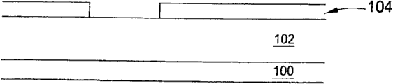
Figure 1A shows an example of low dielectric constant films 102 on substrate 100.Figure 1B shows the photoresist 104 of the composition on low dielectric constant films 102.
For example, subsequently by removing photoresist or ashing treatment is removed photoresist from low dielectric constant films.Fig. 1 C shows by photoresist 104 compositions to form interconnected 106 and the low dielectric constant films 102 of photoresist after being removed.Thin conforma layer 108, promptly thickness is about
 To about
Layer, this layer comprises silicon, carbon, and optionally comprises oxygen and/or nitrogen, is deposited on the low dielectric constant films surface of composition subsequently, shown in Fig. 1 D.Under the condition that RF power exists, this layer can deposit by a kind of admixture of gas of reaction, for example a kind ofly comprises silicon, oxygen, and the admixture of gas of carbon.Silicon, oxygen and carbon are provided by organo-silicon compound, for example octamethylcy-clotetrasiloxane.Organo-silicon compound in typical case with carrier gas injecting chamber.Preferably, carrier gas is a helium.But also can use other inert gases, for example argon gas or nitrogen.
To about
Layer, this layer comprises silicon, carbon, and optionally comprises oxygen and/or nitrogen, is deposited on the low dielectric constant films surface of composition subsequently, shown in Fig. 1 D.Under the condition that RF power exists, this layer can deposit by a kind of admixture of gas of reaction, for example a kind ofly comprises silicon, oxygen, and the admixture of gas of carbon.Silicon, oxygen and carbon are provided by organo-silicon compound, for example octamethylcy-clotetrasiloxane.Organo-silicon compound in typical case with carrier gas injecting chamber.Preferably, carrier gas is a helium.But also can use other inert gases, for example argon gas or nitrogen.
After this layer deposition, will carry out wet-cleaned to substrate, for example use 100: 1HF solution.Subsequently, shown in Fig. 1 E, layer 110, for example PVD (chemical vapour deposition (CVD)) barrier layer or ALD (ald) barrier layer, for instance, ALD tantalum nitride (TaN) layer can be deposited on this layer.Select as another kind, shown in Fig. 1 F, one deck for example stops the layer 120 of antireflecting coating (BARC), will be deposited on the layer 108 and fills interconnected 106.
Under the situation that RF power exists, in chemical vapor deposition chamber or plasma reinforced chemical vapour deposition chamber, by making a kind of reaction gas starting mixture that includes organic silicon compound, deposition comprises silicon/carbon, and optionally comprises the layer of oxygen and/or nitrogen.The example that can be used for depositing the chamber of this layer comprises: have two independent process zones
 Chamber and
Chamber, these two kinds of chambers can be from Santa Clara, the Applied Materials of California, commercially available the buying of Inc. (Applied Materials of the Santa Clara in California).In these process conditions that provide is for having the 300mm PRODUCER in two individual processing zones
@Chamber and providing.Thereby the flow velocity of each substrate processing zone and each substrate is half of flow velocity in the chamber.
Chamber and
Chamber, these two kinds of chambers can be from Santa Clara, the Applied Materials of California, commercially available the buying of Inc. (Applied Materials of the Santa Clara in California).In these process conditions that provide is for having the 300mm PRODUCER in two individual processing zones
@Chamber and providing.Thereby the flow velocity of each substrate processing zone and each substrate is half of flow velocity in the chamber.
In typical case, in the chamber, in described layer of process that is deposited on the substrate, substrate temperature is maintained between about 150 ℃ to about 400 ℃.The performance number that is used for the RF power that the 300mm substrate provides is about 100W or lower, for example at about 30W between about 75W.Generally speaking, the about 0.109W/cm of RF power
2Or lower providing, for example at about 0.033W/cm
2To about 0.082W/cm
2Between.RF power will be provided to shower nozzle, for example, and gas distributing device, and/or the substrate support of chamber.Providing RF power with the high-frequency between about 13MHz to 14MHz, is 13.56MHz under the preferred situation.That RF power can be the cycle or pulse.RF power also can be continuous or discontinuous.Interval between shower nozzle and the substrate support is greater than about 200mil, for example at about 200mil between about 1400mil.Pressure in the chamber is about 1.5Torr or higher, for example at about 1.5Torr between about 8Torr.
The organo-silicon compound approximately flow velocity of 100sccm between about 1000sccm inject this chamber.Carrier gas will be injected this chamber with the flow velocity of about 100sccm between about 7000sccm.In cavity, organosilicon compound flow rate, for example octamethylcy-clotetrasiloxane (OMCTS, sccm), with the flow velocity of carrier gas, helium (sccm) for example, ratio be about 0.1 or higher.According to the depth-to-width ratio of the substrate of composition, this layer may deposit a period of time, such as time range between 0.1 second to 600 seconds, with deposit thickness approximately
 To about
 Between layer.In typical case, when using more high-aspect-ratio, the deposition of this layer needs the longer time so that shaped surfaces to be provided.
Have now found that, use above-mentioned RF performance number, at interval, pressure and velocity ratio, when using a kind of self-saturation organo-silicon compound as predecessor, deposit thickness is only approximately reliably
 To about
 Between thin, conforma layer uniformly.Be applied in the condition that this provides, obtained that thickness range is in single 300mm substrate
 Layer.As said, " self-saturation predecessor " is to deposit skim on substrate, for example, do not consider only molecular layer of predecessor under the sedimentation time length.Thickness can be controlled by the selection of predecessor, because different predecessors has different molecular dimensions, causes the different-thickness of the molecular layer of different predecessors.The existence of this thin layer has hindered predecessor under the process conditions of this thin layer and further has been deposited as extra play being used to deposit.Generally speaking, the self-saturation predecessor comprises methyl, selects for use this methyl to suppress this thin layer continued growth.OMCTS is a kind of self-saturation predecessor of first-selection, because it comprises a large amount of methyl, these methyl cause the self-saturation deposition of one deck, and it goes up the rich carbon film surface that further deposits because the carbon in the methyl family provides abundant inhibition.That is to say, can deposit conformal ground floor, because in a single day subcovering is divided by OMCTS in the surface of below substrate, at the sedimentary deposit surface Si-CH of institute by OMCTS
3The existence of key just provides and suppresses the further carbon-rich surface of deposition, removes by the processing of some other this layer until some methyl groups.Thereby, just can control the deposition of each molecular layer of OMCTS well, this will improve the step coverage of final layer.
Layer.As said, " self-saturation predecessor " is to deposit skim on substrate, for example, do not consider only molecular layer of predecessor under the sedimentation time length.Thickness can be controlled by the selection of predecessor, because different predecessors has different molecular dimensions, causes the different-thickness of the molecular layer of different predecessors.The existence of this thin layer has hindered predecessor under the process conditions of this thin layer and further has been deposited as extra play being used to deposit.Generally speaking, the self-saturation predecessor comprises methyl, selects for use this methyl to suppress this thin layer continued growth.OMCTS is a kind of self-saturation predecessor of first-selection, because it comprises a large amount of methyl, these methyl cause the self-saturation deposition of one deck, and it goes up the rich carbon film surface that further deposits because the carbon in the methyl family provides abundant inhibition.That is to say, can deposit conformal ground floor, because in a single day subcovering is divided by OMCTS in the surface of below substrate, at the sedimentary deposit surface Si-CH of institute by OMCTS
3The existence of key just provides and suppresses the further carbon-rich surface of deposition, removes by the processing of some other this layer until some methyl groups.Thereby, just can control the deposition of each molecular layer of OMCTS well, this will improve the step coverage of final layer.
Except that octamethylcy-clotetrasiloxane, other available predecessors comprise diethoxy methyl-monosilane (DEMS), HMDO (HMDOS), and hexamethyldisilane (HMDS).Other comprise Si, C, and the predecessor of H can be used for this technology, for example trimethyl silane, tetramethylsilane, or the like.
Be not exposed on the low dielectric constant films of cineration technics, and carrying out x-ray photoelectron spectroscopy (XPS) on the low dielectric constant films of photoresist ashing and analyze being exposed to.Also carry out XPS analysis on the low dielectric constant films that is exposed to photoresist ashing and is handled by the thin layer that deposits on it subsequently, according to the embodiment of the present invention, this thin layer is by the OMCTS deposition and comprise silicon, carbon, and oxygen.XPS analysis shows, this veneer on the low dielectric constant films of ashing, is not compared at the low dielectric constant films of handling by deposit film on it through stringer on the low dielectric constant films of ashing, and higher carbon content (carbon atom %) is provided.For example, may have about 3 carbon atom % through the low dielectric constant films of ashing, and provide about 15 carbon atom % from the teeth outwards without the film on the low dielectric constant films of ashing.Thereby from one side, this thin layer is an enriched carbon layer.The carbon content of this thin layer at about 5 carbon atom % between about 30 carbon atom %.Podzolic process consumes the concentration of carbon on the surface of low dielectric constant films, yet this thin layer of deposition has recovered surface carbon concentration on the low-k thin layer of ashing.
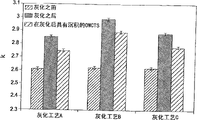
XPS analysis has shown that also the oxygen content with the low dielectric constant films surface of handling with this thin layer is lower than the oxygen content on those low dielectric constant films surfaces that this thin layer of no use is handled after ashing, because the thin layer of the involved carbon of the OH of ashing film surface base replaces.Replacing with the thin layer that comprises carbon, the OH base of ashing film surface has also reduced the dielectric constant of ashing film.Fig. 2 shows on low dielectric constant films and to use the OMCTS stringer and reduced through dielectric constant after the ashing of the film of a technology in three different cineration technicss.
Before the ashing and the angle of wetting that is used for low dielectric constant films after the ashing (be respectively ELKILD at Fig. 3, promptly extremely low k interlayer dielectric medium, and the ELK ILD of ashing), and after the ashing and the low dielectric constant films that has thin OMCTS layer on it also obtain measuring.Its result as shown in Figure 3.In Fig. 3, deposition of thin OMCTS layer has increased the angle of wetting of low dielectric constant films on the low dielectric constant films after the ashing.The angle of wetting that increases shows that thin OMCTS layer has increased the hydrophobicity on low dielectric constant films surface.Hydrophobic described raising is the result that expectation obtains, because hydrophobic surface can prevent moisture adsorption in low dielectric constant films, this absorption will influence film performance or cause needs to add some at least and be used to remove the step consuming time of moisture.
After the wet-cleaned, the effect of deposition of thin conforma layer has also obtained check on interconnected section after the ashing.After film is immersed in 100: 1 the HF solution in wet clean process, the tunnel section in the low zone of tunnel density is high in the low dielectric constant films that has or do not have thin OMCTS layer zone and tunnel density is tested.
Fig. 4 A-4C shows the tunnel section in the high zone of tunnel density.Fig. 4 A shows after the ashing and the tunnel section before the wet-cleaned.Fig. 4 B and 4C show after the ashing and after wet-cleaned, the tunnel section when low dielectric constant films has and do not have thin OMCTS layer respectively.Fig. 4 B shows in the low dielectric constant films tunnel that does not have thin OMCTS layer thereon, and wet-cleaned will cause the critical dimension loss of about 30nm.Fig. 4 C shows before wet-cleaned in the low dielectric film of deposition of thin OMCTS layer on it will can not observe such CD loss.
Fig. 5 A-5C shows the tunnel section in the low zone of tunnel density.Fig. 5 A shows after the ashing and the tunnel section before the wet-cleaned.Fig. 5 B and 5C show after the ashing and behind wet etching, the tunnel section when low dielectric constant films has and do not have thin OMCTS layer respectively.Fig. 5 B shows in the low dielectric constant films tunnel that does not have thin OMCTS layer thereon, and wet-cleaned will cause greater than the approximately undercutting of 30nm.Fig. 5 C shows before wet-cleaned in the low dielectric film of deposition of thin OMCTS layer on it will can not observe such undercutting.
Therefore, this thin OMCTS layer provides a carbon-rich surface, itself so that a hydrophobic surface that is used for preventing low k value film in the loss and the undercutting of wet etch process critical dimension can be provided.
We as can be seen, according to the thin layer that embodiment of the present invention provided, the role who has served as fine and close sealing of hole layer, can be used for stoping BARC material such as depositing the BARC layer after being used as, and as after a kind of PVD of deposited barrier layer stop predecessor or a kind of ALD predecessor of ALD TaN predecessor for example, to the infiltration of this veneer porous low k value film thereon.
For example, after through hole etching and first via metal were inlayed photoresist ashing in (damascene) technology, this thin layer can be deposited on the low dielectric constant films.BARC subsequently fills and can carry out on this layer.This thin layer provides and has been used for preventing that the BARC material is penetrated into the sealing of hole layer of insulation film.Then, low dielectric constant films and below stop such as the insulation between the conductor material of copper, with etched so that following electric conducting material, after tunnel etching and photoresist remove, come out.After the etching insulation stops, can use the reduction chemical reaction will clean and stop the conductive surface that is come out, and from this surface, remove oxide such as cupric oxide (CuO) by removing insulation.This thin layer provides a sealing of hole layer, with barrier layer predecessor after stoping, to the infiltration of this low dielectric constant films.
Be in the execution mode that is deposited on this thin layer with the BARC layer after the wet-cleaned substrate, this thin layer can carry out reprocessing with helium (or other inert gases) plasma, with the concentration of carbon on the surface of adjusting this thin layer and the angle of wetting of this thin layer.This angle of wetting can be reduced to about 70 ℃ or still less, to promote the moistening of BARC layer and deposition.Fig. 6 shows the reduction along with the increase angle of wetting of plasma treatment time.Gentle process conditions for example, are used at about 30W to the RF power between about 100W and at the about 100sccm He flow velocity between about 10000sccm extremely, so that plasma treatment will can not be damaged the sealing of hole characteristic of this thin layer.
Adjust surface wettability or contact angle if desired, before other layers that remove the BARC layer deposit, also can carry out the helium plasma reprocessing to thin layer thereon, described other layers are the ALD barrier layer for example.Can use this thin layer of gas with various plasma reprocessing, for example O
2, CO
2, N
2O, NH
3, H
2, helium, nitrogen, argon, or their combination.Plasma post can be improved the characteristic and the character of this laminar surface, for example surface tension and surface contact angle.
In another embodiment, provide a kind of method of controlling interconnected middle metal connecting line critical dimension.Described in the execution mode of front, this method is included in stringer on the low dielectric constant films of composition.Veneer in low dielectric before on the constant film, this low dielectric constant films of composition can comprise an oxygen enrichment or carbon-rich surface.After this layer deposition, will stop being used to depositing the flowing of predecessor of this layer, OMCTS for example, and only by inject carrier gas in chamber, for example He carrier gas is removed any residue predecessor from chamber.Chamber can be purified or drains or chamber is purified and drains.
After chamber is purified and/or drains, in one embodiment, in chamber, carry out oxygen plasma treatment and be deposited on the layer on the substrate and begin next deposition cycle, for example the OMCTS deposition to handle by predecessor.In another embodiment, if require nitrogen doping oxide or SiN layer, can use adding or not add H
2NH
3Plasma treatment.Oxygen plasma can be provided by any oxygen-containing gas that can produce the oxygen-cent red radical of this laminar surface of oxidation.For example, this gas can comprise O
2, CO
2, N
2O, or their combination.Oxygen-containing gas can inject cavity by a certain flow velocity.Oxygen-containing gas will need in a period of time injecting chamber, and this time is between about 0.1 second to about 60 seconds, depends on passage/tunnel composition section.Oxygen plasma will be with frequency 13.56MHz, and the RF power of power between 50W to 1000W is provided in the cavity.But application mix frequency RF power.For plasma treatment is minimized the impact or the infringement of bottom (such as low dielectric constant films), the first-selected low value high-frequency RF power of using, for example at about 30W between about 100W, its corresponding about 0.033W/cm
2To about 0.082W/cm
2Between.
Can stop plasma treatment by stopping oxygen-containing gas inflow chamber.Optionally, can measure the thickness of sedimentary deposit then.Subsequently, recover flowing of predecessor, it is flowed in the chamber, to deposit the additional amount of this thin layer.Purify this chamber and carry out above-mentioned oxygen plasma treatment subsequently.Carry out deposition, purify, and the Multiple Cycle of plasma treatment is until the required thickness that obtains this layer.Be deposited on the thickness of the layer in interconnected by control, can control the thickness of the metal connecting line that in interconnected, deposits subsequently.
In another embodiment, provide a kind of THICKNESS CONTROL on substrate upper strata that will be deposited on about
To about
 Between method.This substrate that may comprise oxygen enrichment or rich nitrogen top layer under the situation that plasma exists, will be exposed under the silicon-containing precursor, to deposit one deck on this substrate, then, use by containing H
2Or do not contain H
2NH
3The plasma that produces, or use to be selected from by one and comprise O
2, CO
2And N
2The plasma that oxygen-containing gas in the group that O forms produces is handled this layer.Above-mentioned substrate is exposed under the silicon-containing precursor with sedimentary deposit, and will continues to carry out repeatedly, reach desirable thickness up to this layer with the process of this layer of plasma treatment.
Between method.This substrate that may comprise oxygen enrichment or rich nitrogen top layer under the situation that plasma exists, will be exposed under the silicon-containing precursor, to deposit one deck on this substrate, then, use by containing H
2Or do not contain H
2NH
3The plasma that produces, or use to be selected from by one and comprise O
2, CO
2And N
2The plasma that oxygen-containing gas in the group that O forms produces is handled this layer.Above-mentioned substrate is exposed under the silicon-containing precursor with sedimentary deposit, and will continues to carry out repeatedly, reach desirable thickness up to this layer with the process of this layer of plasma treatment.
In an execution mode again, provide the method for the high density dielectric isolation pad that a kind of manufacturing comprises arbitrary oxide or nitride.This method comprises, under the situation that plasma exists, under silicon-containing precursor, exposes the substrate of the composition of the grid that comprises oxygen enrichment or rich nitrogen surface, depositing one deck on this grid, and uses then by being selected from and comprises O
2, CO
2, N
2O, nitrogenous gas, and comprise or do not comprise H
2NH
3Group form contain this layer of plasma treatment that oxygen or nitrogenous gas produce.Above-mentioned silicon-containing precursor, and about being controlled at the plasma-treating technology of the method for metal wire critical dimension in the interconnection, can be used for making in the method for high density dielectric isolation pad, and key-course thickness is about
 To about
Between method in.
To about
Between method in.
Although description has been made to embodiments of the present invention in the front, under situation about not deviating from, can design other or further execution mode by the base region of the present invention of following claim regulation.
Claims (18)
1. a method of handling the film on substrate in chamber is characterized in that, comprises:
By having: oxygen ratio or at the silicon between 1: 1 to 1: 2 at the silicon between 1: 1 to 1: 3: on the surface of the film of nitrogen ratio optionally deposit thickness between 4 dust to 100 dusts and the thin layer that comprises silicon and carbon handle this film, wherein the deposition of this layer is included under the condition that RF power exists the predecessor that comprises silicon, carbon and hydrogen is reacted.
2. method according to claim 1 is characterized in that, described predecessor is chosen free trimethyl silane, tetramethylsilane, dimethyldimethoxysil,ne, 1,3-dimethyl disiloxane, 1,1,3,3-tetramethyl disiloxane, HMDO, hexamethyl cyclotrisiloxane, 1,3,5,7-tetramethyl-ring tetrasiloxane, octamethylcy-clotetrasiloxane and 1,3,5,7, the group that 9-pentamethyl D5 is formed.
3. method according to claim 1 is characterized in that described predecessor comprises alkyl, selects this alkyl to suppress the continued growth of described thin layer.
4. method according to claim 1 is characterized in that, described thin layer has with the surface of described film compares higher carbon content, and described thin layer is for providing a carbon saturated surface layer on the described film simultaneously.
5. method according to claim 1 is characterized in that, further is included in the described substrate of wet-cleaned behind the described veneer.
6. method according to claim 1 is characterized in that, the performance number of the RF power that provides is at 0.109W/cm
2Or it is lower.
7. method according to claim 1 is characterized in that, the pressure in the described chamber is 1.5Torr or higher.
8. method according to claim 1 is characterized in that, being spaced apart greater than 200mil between the substrate support in shower nozzle and the described chamber in the described chamber.
9. method according to claim 1 is characterized in that, further comprises using the described thin layer of a kind of gaseous plasma reprocessing, and described gas is selected from by O
2, CO
2, N
2O, NH
3, H
2, the group formed of helium, argon and nitrogen.
10. method according to claim 1, it is characterized in that, further comprise the described thin layer of plasma reprocessing, wherein said plasma post has changed the surface characteristic of described thin layer, and wherein said surface characteristic is selected from the group of being made up of surface tension and surface contact angle.
11. method according to claim 1 is characterized in that, further is included in deposition end antireflecting coating on the described thin layer.
12. method according to claim 1 is characterized in that, further comprises the deposited barrier layer on described thin layer by ald or physical vapour deposition (PVD).
13. deposit the method for the substrate of low K dielectrics film on the treatment surface, comprising:
Under the condition that RF power exists, by making predecessor react the layer that optionally has the carbon content between 5 carbon atom % to 30 carbon atom % in deposition on the surface of described low K dielectrics film, wherein said predecessor comprises the element of the group of being made up of silicon, carbon, oxygen and nitrogen, the thickness of described layer is between 4 dust to 100 dusts, and the surface of described low K dielectrics film has at the silicon between 1: 1 to 1: 3: oxygen ratio or the silicon between 1: 1 to 1: 2: nitrogen ratio.
14. method according to claim 13 is characterized in that, described predecessor is self-saturating.
15. method according to claim 13 is characterized in that, described predecessor is chosen free trimethyl silane, tetramethylsilane, dimethyldimethoxysil,ne, 1,3-dimethyl disiloxane, 1,1,3,3-tetramethyl disiloxane, HMDO, hexamethyl cyclotrisiloxane, 1,3,5,7-tetramethyl-ring tetrasiloxane, octamethylcy-clotetrasiloxane and 1,3,5,7, the group that 9-pentamethyl D5 is formed.
16. method according to claim 13 is characterized in that, further comprises using the described layer of a kind of gaseous plasma reprocessing, described gas is selected from by O
2, CO
2, N
2O, NH
3, H
2, the group formed of helium, argon and nitrogen.
17. a method of handling the film on the substrate in chamber comprises:
Under the condition that RF power exists, by predecessor is reacted, with thickness between 4 dust to 100 dusts and have on the surface that is deposited upon described substrate of the carbon content between 5 carbon atom % to the 30 carbon atom %, wherein said predecessor comprises the element of choosing from the group of being made up of silicon, carbon, oxygen and nitrogen, and wherein said surface has at the silicon between 1: 1 to 1: 3: oxygen ratio or the silicon between 1: 1 to 1: 2: nitrogen ratio.
18. method according to claim 17 is characterized in that, further comprises described layer is exposed to plasma, described plasma is by being selected from by O
2, CO
2, N
2O, NH
3, H
2, the group formed of helium, argon and nitrogen compound form.
Applications Claiming Priority (3)
| Application Number | Priority Date | Filing Date | Title |
|---|---|---|---|
| US86677006P | 2006-11-21 | 2006-11-21 | |
| US60/866,770 | 2006-11-21 | ||
| US11/694,856 | 2007-03-30 |
Publications (2)
| Publication Number | Publication Date |
|---|---|
| CN101202227A CN101202227A (en) | 2008-06-18 |
| CN100550318C true CN100550318C (en) | 2009-10-14 |
Family
ID=39517296
Family Applications (1)
| Application Number | Title | Priority Date | Filing Date |
|---|---|---|---|
| CNB2007101651423A Expired - Fee Related CN100550318C (en) | 2006-11-21 | 2007-10-29 | Minimize wet etching undercutting degree and the method for extremely hanging down K value (K<2.5) dielectric sealing of hole is provided |
Country Status (4)
| Country | Link |
|---|---|
| JP (1) | JP5174435B2 (en) |
| KR (1) | KR100939593B1 (en) |
| CN (1) | CN100550318C (en) |
| TW (1) | TWI392024B (en) |
Cited By (1)
| Publication number | Priority date | Publication date | Assignee | Title |
|---|---|---|---|---|
| CN102543850A (en) * | 2010-11-17 | 2012-07-04 | 应用材料公司 | Method of processing low K dielectric films |
Families Citing this family (9)
| Publication number | Priority date | Publication date | Assignee | Title |
|---|---|---|---|---|
| US8236684B2 (en) * | 2008-06-27 | 2012-08-07 | Applied Materials, Inc. | Prevention and reduction of solvent and solution penetration into porous dielectrics using a thin barrier layer |
| CN101740332B (en) * | 2008-11-13 | 2012-04-25 | 中芯国际集成电路制造(北京)有限公司 | Etching method of semiconductor element |
| US9034770B2 (en) * | 2012-09-17 | 2015-05-19 | Applied Materials, Inc. | Differential silicon oxide etch |
| CN103839871B (en) * | 2012-11-21 | 2017-09-08 | 中芯国际集成电路制造(上海)有限公司 | A kind of manufacture method of semiconductor devices |
| CN105448705B (en) * | 2014-06-18 | 2018-05-04 | 无锡华润上华科技有限公司 | The method and its oxide-film of particulate on a kind of elimination chip oxide film |
| CN105244257B (en) * | 2014-07-08 | 2020-06-23 | 中芯国际集成电路制造(上海)有限公司 | Method for improving protrusion defect of porous low-k film |
| CN105702619A (en) * | 2014-11-27 | 2016-06-22 | 中芯国际集成电路制造(上海)有限公司 | Formation method of semiconductor structure |
| CN111863610A (en) * | 2020-05-12 | 2020-10-30 | 中国电子科技集团公司第十一研究所 | Method for preparing electrode hole and computer readable storage medium |
| CN113667976A (en) * | 2021-08-27 | 2021-11-19 | 中国科学院兰州化学物理研究所 | Corrosion-resistant DLC film with hole sealing top layer and preparation method thereof |
Family Cites Families (14)
| Publication number | Priority date | Publication date | Assignee | Title |
|---|---|---|---|---|
| JP2001077196A (en) * | 1999-09-08 | 2001-03-23 | Sony Corp | Manufacture of semiconductor device |
| TW535253B (en) * | 2000-09-08 | 2003-06-01 | Applied Materials Inc | Plasma treatment of silicon carbide films |
| US6890850B2 (en) * | 2001-12-14 | 2005-05-10 | Applied Materials, Inc. | Method of depositing dielectric materials in damascene applications |
| US6936551B2 (en) * | 2002-05-08 | 2005-08-30 | Applied Materials Inc. | Methods and apparatus for E-beam treatment used to fabricate integrated circuit devices |
| US6927178B2 (en) * | 2002-07-11 | 2005-08-09 | Applied Materials, Inc. | Nitrogen-free dielectric anti-reflective coating and hardmask |
| US7005390B2 (en) * | 2002-10-09 | 2006-02-28 | Intel Corporation | Replenishment of surface carbon and surface passivation of low-k porous silicon-based dielectric materials |
| KR100909175B1 (en) * | 2002-12-27 | 2009-07-22 | 매그나칩 반도체 유한회사 | How to form a dual damascene pattern |
| KR100573484B1 (en) * | 2003-06-30 | 2006-04-24 | 에스티마이크로일렉트로닉스 엔.브이. | Semiconductor device and a method of forming the same |
| KR20050014231A (en) * | 2003-07-30 | 2005-02-07 | 매그나칩 반도체 유한회사 | A method for forming a semiconductor device |
| JP2005050954A (en) * | 2003-07-31 | 2005-02-24 | Toshiba Corp | Semiconductor device and manufacturing method therefor |
| US20050037153A1 (en) * | 2003-08-14 | 2005-02-17 | Applied Materials, Inc. | Stress reduction of sioc low k films |
| JP4015976B2 (en) * | 2003-08-28 | 2007-11-28 | 株式会社東芝 | Manufacturing method of electronic device |
| JP2005203568A (en) * | 2004-01-15 | 2005-07-28 | Semiconductor Leading Edge Technologies Inc | Fabrication process of semiconductor device, and semiconductor device |
| JP2006332408A (en) * | 2005-05-27 | 2006-12-07 | Sony Corp | Manufacturing method of semiconductor device |
-
2007
- 2007-10-26 KR KR1020070108170A patent/KR100939593B1/en not_active IP Right Cessation
- 2007-10-29 CN CNB2007101651423A patent/CN100550318C/en not_active Expired - Fee Related
- 2007-10-29 TW TW096140628A patent/TWI392024B/en active
- 2007-11-16 JP JP2007298307A patent/JP5174435B2/en active Active
Cited By (1)
| Publication number | Priority date | Publication date | Assignee | Title |
|---|---|---|---|---|
| CN102543850A (en) * | 2010-11-17 | 2012-07-04 | 应用材料公司 | Method of processing low K dielectric films |
Also Published As
| Publication number | Publication date |
|---|---|
| KR100939593B1 (en) | 2010-02-01 |
| CN101202227A (en) | 2008-06-18 |
| KR20080046087A (en) | 2008-05-26 |
| TW200826196A (en) | 2008-06-16 |
| TWI392024B (en) | 2013-04-01 |
| JP5174435B2 (en) | 2013-04-03 |
| JP2008147644A (en) | 2008-06-26 |
Similar Documents
| Publication | Publication Date | Title |
|---|---|---|
| CN100550318C (en) | Minimize wet etching undercutting degree and the method for extremely hanging down K value (K<2.5) dielectric sealing of hole is provided | |
| KR102406467B1 (en) | Remote Plasma Based Deposition of Graded Silicon Carbide Films or Multilayer Silicon Carbide Films | |
| US8445075B2 (en) | Method to minimize wet etch undercuts and provide pore sealing of extreme low k (k<2.5) dielectrics | |
| US10472714B2 (en) | Method to obtain SiC class of films of desired composition and film properties | |
| CN100431110C (en) | Low-dielectric silicon nitride film and method of making the same, seimiconductor device and fabrication process thereof | |
| CN103975419B (en) | Plasma activated conformal dielectric film deposition | |
| KR101528832B1 (en) | Manufacturing method of flowable dielectric layer | |
| KR101183641B1 (en) | Methods to obtain low k dielectric barrier with superior etch resistivity | |
| US8927442B1 (en) | SiCOH hardmask with graded transition layers | |
| US20100055442A1 (en) | METHOD OF PE-ALD OF SiNxCy AND INTEGRATION OF LINER MATERIALS ON POROUS LOW K SUBSTRATES | |
| KR20050034566A (en) | Method of manufacturing silicon carbide film | |
| TWI517298B (en) | Controlled air gap formation | |
| US8889235B2 (en) | Dielectric barrier deposition using nitrogen containing precursor | |
| US20120070957A1 (en) | Air gap formation | |
| KR20020007224A (en) | Method and apparatus for treating l0w k dielectric layers to reduce diffusion | |
| KR101327640B1 (en) | Method for forming a dielectric film and novel precursors for implementing said method | |
| JP2012510726A (en) | Deposition of dielectric barriers using oxygen-containing precursors | |
| KR20050091780A (en) | Method and apparatus to improve cracking thresholds and mechanical properties of low-k dielectric material |
Legal Events
| Date | Code | Title | Description |
|---|---|---|---|
| C06 | Publication | ||
| PB01 | Publication | ||
| C10 | Entry into substantive examination | ||
| SE01 | Entry into force of request for substantive examination | ||
| C14 | Grant of patent or utility model | ||
| GR01 | Patent grant | ||
| C56 | Change in the name or address of the patentee | ||
| CP01 | Change in the name or title of a patent holder |
Address after: American California Patentee after: Applied Materials Inc. Address before: American California Patentee before: Applied Materials Inc. |
|
| CF01 | Termination of patent right due to non-payment of annual fee |
Granted publication date: 20091014 Termination date: 20141029 |
|
| EXPY | Termination of patent right or utility model |