CN100527933C - Electronic component identification process and apparatus - Google Patents
Electronic component identification process and apparatus Download PDFInfo
- Publication number
- CN100527933C CN100527933C CNB2004101016906A CN200410101690A CN100527933C CN 100527933 C CN100527933 C CN 100527933C CN B2004101016906 A CNB2004101016906 A CN B2004101016906A CN 200410101690 A CN200410101690 A CN 200410101690A CN 100527933 C CN100527933 C CN 100527933C
- Authority
- CN
- China
- Prior art keywords
- electronic device
- image recognition
- image
- data
- coaxial
- Prior art date
- Legal status (The legal status is an assumption and is not a legal conclusion. Google has not performed a legal analysis and makes no representation as to the accuracy of the status listed.)
- Expired - Fee Related
Links
Images


Landscapes
- Supply And Installment Of Electrical Components (AREA)
Abstract
Provided is a method and a device for recognizing an electronic part by which, even when the suction position of a nozzle is photographed while it is out of the center of a chip, the chip can be recognized accurately. The electronic part mounting device (10) is provided with a lower lighting fitting (25) and a side lighting fitting (27) in addition to coaxial lighting fitting (23) to direct light while changing an angle of lighting, and it also determines based on image recognition processing whether or not the lower surface of the nozzle is photographed, and a projecting area from the chip sucked to the nozzle is reduced without giving an influence to the image recognition processing, and then the photographed image is picked up to generate image recognition data through the image recognition processing.
Description
Technical field
The present invention relates to be adsorbed and remain on the image that the electronic device on the suction nozzle obtains, the electronic component identification process and the device that the position of electronic device are carried out image recognition according to taking from the below.
Background technology
In electronic device manufacturing field,, be extensive use of the method for application image identification as the method for localized electron device and substrate accurately.This method is taken the image that obtains by identification to substrate and electronic device, detects the substrate sign of substrate and the positions such as electrode, edge part or center of gravity portion of electronic device.
In the position probing of the electronic device of this image recognition, with electronic device absorption with remain on the suction nozzle, it is moved above camera head, and take with the CCD camera.But, in recent years the circuit arrangement substrate is required high density, high precision int, and adopt chip device mostly as electronic device, also realized the microminiaturization of chip device.Therefore, take if depart from the absorption position of suction nozzle under the state at chip device center, then shown in Fig. 5 (a), the suction nozzle lower surface that exposes from chip device also is taken into, so can't correctly carry out image recognition.
Therefore, the adsorption plane of suction nozzle of absorption chip device is carried out black handle, applying Vickers hardness in the black treatment surface is more than or equal to 2000kg/mm
2Hard carbon film.In addition, above-mentioned hard carbon film is known as the DLC film.Handle by black, the part of exposing from the chip device that is adsorbed on the suction nozzle is not taken into, and can prevent that by applying the DLC film black from handling come off (for example, with reference to the patent documentation 1) that be worn.
And, because according to the size of chip device and lead-in wire at interval etc. and different at the shooting optimal brightness that is used for device identification, so, as the device that obtains suitable image, be the difference that adopts by part category, the adjusted value of storage illumination light, correspondence is attracted to the device on the suction nozzle, read the adjusted value of storage, according to the light quantity (for example, with reference to patent documentation 2) of adjusted value control illumination.
[patent documentation 1] spy opens flat 6-No. 244592 communiques
No. 3308228 communique of [patent documentation 2] special permission
Yet the thickness of DLC membrane coat is approximately 1 μ m, and in the process of the absorption that reaches the inferior chip device of hundreds of thousands repeatedly, maintenance, assembling, and the wearing and tearing between the chip device will cause coming off of coating and black handling part.And the light quantity that only depends on control to throw light on can not be avoided the reverberation from the suction nozzle lower surface, thereby exists the problem that can't accurately carry out image recognition owing to the part of exposing from the chip device that is adsorbed on the suction nozzle is taken into.
Summary of the invention
The object of the present invention is to provide a kind of electronic component identification process and device, promptly except coaxial-illuminating, below illumination and side illumination also are set, in conversion light angle irradiates light, judge whether be ingested below the suction nozzle by image recognition processing, read and to reduce to the image of taking after the degree that does not influence image recognition processing from the part that expose of chip device of absorption, thereby reduce the generation of identification error.Therefore, the objective of the invention is to,, also can correctly and effectively carry out image recognition even coating and black handling part are ground off.
In order to solve the above problems, one of the present invention adopts under the state on a kind of adsorption plane that is adsorbed and remains on suction nozzle at electronic device, by to described electronic device irradiates light and take, image to described electronic device carries out image recognition processing, carry out the electronic component identification process of electronic device assembly machine of the assembling of electronic device, this method is under the situation of preassigned device at described electronic device, throw light on irradiates light with the below, take described device, generate shape and relatively use data by the image that utilizes the illumination of described below to take being carried out image recognition processing, described shape is relatively compared with data and preassigned value, if within permissible range, transmitted image recognition data then, described shape is relatively compared with data and preassigned value, if outside permissible range, then come irradiates light with side illumination, take described device once more, generate shape and relatively use data by the image that utilizes described side illumination to take being carried out image recognition processing, described shape is relatively compared with data and preassigned value, if within permissible range, transmitted image recognition data then, described shape is relatively compared with data and preassigned value, if should be worth outside permissible range, then transmit mistake.
And the present invention's two is characterised in that, in the image-recognizing method of electronic device assembly machine one of of the present invention, if described electronic device is not preassigned device, just come irradiates light with coaxial-illuminating, take described electronic device, the image that uses described coaxial-illuminating to take is carried out image recognition processing, the transmitted image recognition data.
In addition, in order to solve the above problems, the present invention's three constitutes under the state on a kind of adsorption plane that is adsorbed and remains on suction nozzle at electronic device, by to described electronic device irradiates light and take, image to described electronic device carries out image recognition processing, carry out the electronic device recognition device of electronic device assembly machine of the assembling of electronic device, it comprises: lighting unit has coaxial-illuminating portion, below Lighting Division, side illumination portion to described electronic device irradiates light; The illumination switch unit switches the driving to the described Lighting Division of described lighting unit; Store the image storage unit of captured image; Data storage cell is extracted the needed view data of image recognition processing out and is stored from described image storage unit; The identification arithmetic element is carried out image recognition processing to the view data that is stored in the described data storage cell, generates shape and relatively uses data; The shape comparing unit relatively compares described shape with data and preassigned value; Control unit according to the comparative result of described shape comparing unit, transmits the handled image recognition data of described identification arithmetic element, perhaps controls described illumination switch unit.
Image-recognizing method and device according to electronic device assembly machine of the present invention, at the electronic device that is adsorbed is under the situation of preassigned device (for example chip device), at first take to the chip device irradiates light, and carry out image recognition processing with the below illumination.Then, judge that the shape of photographic images is whether in preassigned scope.If outside specified scope, then use side illumination to take to the chip device irradiates light, carry out image recognition processing.Whether the shape of judging photographic images afterwards is in preassigned scope.Like this, the part that only adopts the captured suction nozzle that is adsorbed state to expose from chip device does not influence the image of image recognition processing, this image is carried out image recognition processing, then, send the image recognition data main control unit of electronic device assembly machine to, thereby can reduce identification error significantly.
In addition, also have coaxial-illuminating,, can use coaxial-illuminating to take, and carry out image recognition processing to the electronic device irradiates light at appointed device (for example chip device) large-scale electronic device in addition in advance.Therefore can reduce the image recognition time, can send the image recognition data that do not have identification error to the main control unit of electronic device assembly machine.
Description of drawings
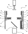
Fig. 1 is the stereogram that has disposed the electronic device assembly machine of electronic device recognition device.
Fig. 2 is the figure of the lighting unit of expression electronic device recognition device.
Fig. 3 is the block diagram of expression system configuration.
Fig. 4 is the flow chart that expression utilizes the electronic device identification maneuver of image processing.
Fig. 5 is the figure of the image of the part exposed from chip device of the suction nozzle of expression chip device and absorption chip device.
Among the figure: 10-electronic device assembly machine; 11-assembles head; The 12-XY transport unit; 13-board carrying road; The 14-electronic device supplier; 15-electronic device recognition device; The appointed in advance device of 18-(for example chip device); The 19-substrate; The 20-lighting device; 23-coaxial-illuminating portion; 25-below Lighting Division; 27-side illumination portion; The 29-CCD camera; The 31-A/D converter section; The 32-image storage unit; The 33-data storage cell; 34-discerns arithmetic element; 35-shape comparing unit; The 36-control unit; The 37-switch unit that throws light on; The 38-main control unit.
Embodiment
Below, with reference to accompanying drawing an embodiment of the invention are described.Fig. 1 is the stereogram as the electronic device assembly machine that disposes recognition device of an embodiment of the invention.Fig. 2 is the lighting unit of electronic device recognition device, Fig. 3 is the block diagram of expression system configuration, Fig. 4 is the flow chart of action that expression has utilized the electronic device recognition device of image processing, and Fig. 5 is the image graph of the part of exposing from chip device of expression chip device and the suction nozzle that is adsorbed with chip device.
At first, with reference to Fig. 1, the overall structure of electronic device assembly machine 10 is described.Among Fig. 1,13 is the board carrying road.Near the central portion on board carrying road 13, keeping by the next substrate 19 of board carrying road 13 carryings.Assembling head 11 is supported on the XY transport unit 12, can move horizontally.Be equipped with the suction nozzle of absorption and maintenance electronic device on the assembling head 11.Assembling head 11 is useful on to the electronic device of electronic device supplier (filter) 14 in the bottom of this suction nozzle vacuum suction and supplies with the electronic device (chip device) 18 that the position is supplied with, and carries out XY and move above electronic device recognition device 15.Below the electronic device recognition device 15 shooting chip devices, absorption side-play amount (XY error, angular error) according to image recognition processing computing absorption and the chip device that keeps, and carry out position correction with respect to the regular allocation position of substrate 19, be configured on the substrate 19.
With reference to Fig. 2, the structure of the lighting unit 20 of electronic device recognition device 15 is described.The lighting unit 20 that constitutes by coaxial-illuminating portion 23, below Lighting Division 25, side illumination portion 27 shown in Fig. 2.
In coaxial-illuminating portion 23, a plurality of LED21 are two dimension (plane) and arrange, and this coaxial-illuminating portion is installed in as on the vertical dull and stereotyped framework 22, make the arrangement plane of LED21 be vertical state.Part about framework 22 shows among the figure, but in fact also dispose in front and back, constituted the structure of enclosing Lighting Division.On the caustic surface of coaxial-illuminating portion 23, dispose scatter plate 24, so that form uniform illumination light.
Intersection point portion at the horizontal direction center line of the vertical center line in the space that is surrounded by framework 22 and coaxial-illuminating portion 23 disposes the half-reflecting mirror 28 that forms miter angle with respect to coaxial-illuminating portion 23.The illumination light that sees through scatter plate 24 is reflected upward by half-reflecting mirror 28, under to chip device 18 irradiates lights that are adsorbed and remain on the suction nozzle 16.And, utilize CCD camera 29 to take chip device 18 downwards by the light transmission half-reflecting mirror 28 that chip device 18 reflects.
Below in the Lighting Division 25, a plurality of LED21 are two dimension (plane) and arrange, this below Lighting Division is installed on the framework 22, makes the arrangement plane of LED21 be horizontal state, and on the top of coaxial-illuminating portion 23.Part about below Lighting Division 25 shows among the figure, but in fact also dispose in front and back, constitute the structure of surrounding Lighting Division.In addition, the inside edge portion of each below Lighting Division 25 (opposition side of the edge part of close framework 22) forms the size in the visual field that does not enter CCD camera 29.Below the upper surface of Lighting Division 25 dispose and be used to form uniform illumination light scatter plate 26, the illumination light that sees through scatter plate 2 is from tiltedly direction absorption and remain on chip 18 irradiates lights on the suction nozzle 16 down.And, take chip device 18 downwards with CCD camera 29 by the light transmission half-reflecting mirror 28 that chip device 18 reflects.
In side illumination portion 27, a plurality of LED21 are two dimension (plane) configuration, and this side illumination portion is vertical state configuration on framework 22 with the arrangement plane of LED 21, and are positioned at the top of below Lighting Division 25.Part about side illumination portion 27 shows among the figure, but in fact also be configured in front and back, constitute the structure of surrounding Lighting Division.In addition, in order not hinder the illumination of below Lighting Division 25, side illumination portion 27 is configured in the arrangement outside (near a side of framework 22) of the LED21 of below Lighting Division 25.Illumination light shines absorption and remains on the chip device 18 on the suction nozzle 16 from oblique below.And, utilize CCD camera 29 to take chip device 18 downwards by the light transmission half-reflecting mirror 28 that chip device 18 reflects.
Below, with reference to Fig. 3 the structure of the control system of electronic device recognition device 10 is described.
Among Fig. 2, CCD camera 29 is taken electronic device 18, and sends view data to image storage unit 32 through A/D converter section 31.The view data that image storage unit 32 storages were changed through A/D.And, carry out the data of image processing section from image storage unit 32 extractions, and be stored in the data storage cell 33 in order to shorten the image recognition processing time.
The view data that 34 pairs of arithmetic elements of identification are stored in the data storage cell 33 is carried out image recognition processing, and position and angles such as the electrode of detection electronics, edge part or center of gravity portion.Image recognition processing is according to the kind of device and size and preassigned method is carried out by pattern matching method, binarization method etc.Here be under the situation of chip device at electronic device, generate and to be used for judging that the shape whether suction nozzle is read as image relatively uses data.The method of described generation data can be specified in advance, if pattern matching method then calculates the highest matching rate; If contour tracing method, the then profile length of computed image; If area method, the then area of computed image.
Shape comparing unit 35 receives the shape of being calculated by identification arithmetic element 34 and relatively uses data, and sends the judged result of OK or NG to control unit 36.Under the situation of the highest matching rate, if shape is relatively bigger than preassigned value with data, then be OK, if little then be NG.Under the situation of profile length, if shape relatively uses data in preassigned scope, be OK then, if outside specified scope, then be NG.Under the situation of area, if shape relatively uses data in preassigned scope, then be OK, if outside preassigned scope, then be NG.
The part of control unit 36 for whole electronic device recognition device 15 is controlled, however only describe relating to part of the present invention.If not chip device, then control unit 36 obtains the position such as electrode, edge part or center of gravity portion of electronic device and the view data of angle from identification arithmetic element 34, sends the main control unit 38 of electronic device assembly machine 10 to.Under the situation that is chip device,, then obtain the position of center of gravity portion and the image recognition data of angle, and send the main control unit 38 of electronic device assembly machine 10 to from identification arithmetic element 34 if be OK relatively with the judged result of unit 35.If the judged result of shape comparing unit 35 is NG, then when the control signal of illumination conversion is sent to illumination converting unit 37, send image pickup signal to the CCD camera.
Illumination switch unit 37 is according to the control signal of control unit 36, any one party in coaxial-illuminating portion 23, below Lighting Division 25, the side illumination portion 27 is moved throws light on, combination action is thrown light on, the brightness of illumination is reduced throw light on.
At this, describe with OK and the corresponding image of NG with reference to Fig. 5 pair.Image by the CCD camera is the two-dimensional arrangements of the pixel of m * n, and each pixel has pixel value, and common value is 0~255.CCD is shone the pixel value height of the part of high light, and the pixel value of the part of the irradiation low light level is low.Be by two kinds of color showings of black and white among the figure, can't show pixel value, therefore that black is many parts are represented as the high part of pixel value, and the few part of black is represented as the low part of pixel value.32 is images, the 31st of chip device among Fig. 5 (a), the image below the suction nozzle that exposes.31 and 32 all is pixel value height (black part be'ss many) part.In this case, can't distinguish 31 and 32, can be used as chip to 31 and 32 parts that merge and carry out image recognition, therefore be judged as NG in relatively in shape.In Fig. 5 (b), 31 is the image below the suction nozzle that exposes, and is pixel value low (black be'ss few) part.Owing to can distinguish 31 part from the part of 32 pixel value height (black is many), therefore be 32 as the capable image recognition of chip device, be judged as OK in shape in relatively.By switching Lighting Division, can generate as the image of Fig. 5 (b) and carry out image recognition.
The structure of electronic device recognition device 15 describes its action as previously discussed below.At first, assembling head 11 is adsorbed on electronic device on the suction nozzle and carries out XY and move, so that electronic device is positioned at the top (camera position) of electronic device recognition device 15.Among Fig. 4, whether be that chip device is judged (step ST1) to the electronic device that is adsorbed on the suction nozzle.If not chip device, then make the action of coaxial-illuminating portion, and irradiates light is taken electronic device (step ST9).By image recognition processing, positions such as electrode, edge part and the center of gravity portion of electronic device and angle are sent to the main control unit 38 (step ST11) of electronic device assembly machine 10.
If chip device then makes the below Lighting Division move irradiates light, take chip device (step ST2).By image recognition processing, generate and to be used for judging that whether suction nozzle relatively use data (step ST3) as the shape that image is read.Then, whether be that the shape of being allowed is judged (step ST4) to shape.If the shape of allowing, the image recognition data of the center of gravity portion position of chip device and angle are sent in the main control unit 38 of electronic component device machine 10 (step ST11).
If the shape of not allowing then makes side illumination portion move irradiates light, take chip device (step ST5).Generate by image recognition processing and to be used for judging that whether suction nozzle relatively use data (step ST6) as the shape that image is read.Then, whether be the judgement (step ST7) of admissible set.If admissible set, then the image recognition data of the center of gravity portion position of chip device and angle are sent in the main control unit 38 of electronic component device machine 10 (step ST11).
If the shape of not allowing, mistake is sent in the main control unit 38 of electronic component device machine 10 (step ST8).
In addition, under the situation that is chip device, also can before entering step ST2, step ST1 can insert following several action: make below illumination and side illumination move irradiates light, take chip device; Generate by image recognition processing and to be used for judging that whether suction nozzle relatively use data as the shape that image is read; It whether is the judgement of the shape of allowing.
In addition, before entering step ST5, can insert following several action: make below illumination action,, take chip device so that its brightness becomes is about 1/2, and makes side illumination move irradiates light from step ST4; Generate by image recognition processing and to be used for judging that whether suction nozzle relatively use data as the shape that image is read; It whether is the judgement of the shape of allowing.
In addition, so-called preassigned device is according to the relation of the profile of suction nozzle and size of devices and the device of appointment is not limited to chip device.
Utilize the field as other, also can for example discern, laser diode chip is positioned on the secondary installation base plate (sub mount), in the chips welding technology of assembling by profile to laser diode chip.
Claims (3)
1. the electronic component identification process of an electronic device assembly machine, be adsorbed and remain at electronic device under the state on the adsorption plane of suction nozzle, by to described electronic device irradiates light and take, image to described electronic device carries out image recognition processing, carry out the assembling of electronic device, it is characterized in that, at described electronic device is under the situation of preassigned electronic device, come to described electronic device irradiates light with the below illumination, take described electronic device, generate and be used for judging that whether suction nozzle relatively use data as the shape that image is read by the image that utilizes the illumination of described below to take being carried out image recognition processing, described shape is relatively compared with data and preassigned value, if within permissible range, transmitted image recognition data then, if outside permissible range, then come to described electronic device irradiates light with side illumination, take described electronic device once more, generate another shape and relatively use data by the image that utilizes described side illumination to take being carried out image recognition processing, described another shape is relatively compared with data and preassigned value, if within permissible range, transmitted image recognition data then, if outside permissible range, then transmit mistake.
2. the electronic component identification process of electronic device assembly machine according to claim 1 is characterized in that,
If described electronic device is not preassigned device, then come irradiates light with coaxial-illuminating, take described electronic device, the image that utilizes described coaxial-illuminating to take is carried out image recognition processing, and the transmitted image recognition data.
3. the electronic device recognition device of an electronic device assembly machine, be adsorbed and remain at electronic device under the state on the adsorption plane of suction nozzle, by to described electronic device irradiates light and take, image to described electronic device carries out image recognition processing, carry out the assembling of electronic device, it is characterized in that, comprising:
Lighting unit has coaxial-illuminating portion, below Lighting Division, side illumination portion to described electronic device irradiates light;
The illumination switch unit, any one party in described coaxial-illuminating portion, described below Lighting Division, the described side illumination portion is moved throws light on, described coaxial-illuminating portion, described below Lighting Division, the combination action of described side illumination portion are thrown light on, the brightness of the illumination of described coaxial-illuminating portion, described below Lighting Division, described side illumination portion is reduced throw light on;
Store the image storage unit of captured image;
Data storage cell is extracted the needed view data of image recognition processing out and is stored from described image storage unit;
The identification arithmetic element is carried out image recognition processing to the view data that is stored in the described data storage cell, generates to be used for judging that the shape whether suction nozzle is read as image relatively uses data;
The shape comparing unit relatively compares described shape with data and preassigned value;
Control unit, comparative result according to described shape comparing unit, if within permissible range, then transmit the handled image recognition data of described identification arithmetic element, if outside permissible range, then control described illumination switch unit and make described coaxial-illuminating portion, described below Lighting Division, any one party in the described side illumination portion is moved and is thrown light on, perhaps make described coaxial-illuminating portion, described below Lighting Division, the combination action of described side illumination portion is thrown light on, and perhaps makes described coaxial-illuminating portion, described below Lighting Division, the brightness of the illumination of described side illumination portion reduces throws light on.
Applications Claiming Priority (2)
| Application Number | Priority Date | Filing Date | Title |
|---|---|---|---|
| JP2003421751A JP2005183643A (en) | 2003-12-19 | 2003-12-19 | Method and device for recognizing electronic part |
| JP2003421751 | 2003-12-19 |
Publications (2)
| Publication Number | Publication Date |
|---|---|
| CN1630468A CN1630468A (en) | 2005-06-22 |
| CN100527933C true CN100527933C (en) | 2009-08-12 |
Family
ID=34782838
Family Applications (1)
| Application Number | Title | Priority Date | Filing Date |
|---|---|---|---|
| CNB2004101016906A Expired - Fee Related CN100527933C (en) | 2003-12-19 | 2004-12-20 | Electronic component identification process and apparatus |
Country Status (2)
| Country | Link |
|---|---|
| JP (1) | JP2005183643A (en) |
| CN (1) | CN100527933C (en) |
Families Citing this family (4)
| Publication number | Priority date | Publication date | Assignee | Title |
|---|---|---|---|---|
| CN101877959B (en) * | 2009-04-29 | 2012-10-10 | 三星Techwin株式会社 | Electronic component recognition device and chip mounter therewith |
| WO2014155657A1 (en) * | 2013-03-29 | 2014-10-02 | 富士機械製造株式会社 | Electronic component mounting machine and measurement method |
| WO2018220733A1 (en) * | 2017-05-31 | 2018-12-06 | 株式会社Fuji | Work machine, and calculation method |
| KR102182698B1 (en) * | 2019-01-11 | 2020-11-24 | 한화정밀기계 주식회사 | Apparatus and method for detecting an electronic part |
-
2003
- 2003-12-19 JP JP2003421751A patent/JP2005183643A/en not_active Ceased
-
2004
- 2004-12-20 CN CNB2004101016906A patent/CN100527933C/en not_active Expired - Fee Related
Also Published As
| Publication number | Publication date |
|---|---|
| CN1630468A (en) | 2005-06-22 |
| JP2005183643A (en) | 2005-07-07 |
Similar Documents
| Publication | Publication Date | Title |
|---|---|---|
| US7193697B2 (en) | Apparatus for feature detection | |
| CN1300546C (en) | Illumination device, recognizing device with the illumination device, and part mounting device | |
| CN101384897A (en) | Off-axis illumination assembly and method | |
| JP4922890B2 (en) | Electronic component mounting method | |
| US5999640A (en) | Electronic part mounting apparatus with reflector which optimizes available light | |
| CN100527933C (en) | Electronic component identification process and apparatus | |
| IE960563A1 (en) | A measurement system | |
| KR101079686B1 (en) | Image recognition apparatus and image recognition method | |
| KR100289208B1 (en) | Residual Part Observation Device and Electronic Part Observation Method | |
| JP3372789B2 (en) | Lighting device for surface mounter and method of manufacturing the same | |
| US20040239952A1 (en) | Sensor for visual position detection with a modular lighting unit | |
| EP1079420A2 (en) | Inspection apparatus | |
| KR101408361B1 (en) | A component recognition apparatus for chip mounter | |
| KR101113088B1 (en) | Chip mounter and component recognition method thereof | |
| JP6871953B2 (en) | Lighting condition reproduction camera stand and production job optimization method | |
| JP3877495B2 (en) | Electronic component recognition device | |
| JPH0438405A (en) | Method for recognizing transparent member on tray | |
| JPH06237094A (en) | Method and device for illumination of suction part | |
| JP2002110745A (en) | Component recognition control method and component recognition control apparatus | |
| JP2010087304A (en) | Electronic component mounting apparatus | |
| JPH08222896A (en) | Illuminator for mounting machine | |
| CN100514046C (en) | Image recognition apparatus and image recognition method | |
| JP2002057500A (en) | Method for recognizing electronic component | |
| JPH07174539A (en) | Image-processing apparatus | |
| JP3783680B2 (en) | Electronic component observation apparatus and electronic component observation method |
Legal Events
| Date | Code | Title | Description |
|---|---|---|---|
| C06 | Publication | ||
| PB01 | Publication | ||
| C10 | Entry into substantive examination | ||
| SE01 | Entry into force of request for substantive examination | ||
| C14 | Grant of patent or utility model | ||
| GR01 | Patent grant | ||
| C17 | Cessation of patent right | ||
| CF01 | Termination of patent right due to non-payment of annual fee |
Granted publication date: 20090812 Termination date: 20101220 |