CN100472281C - Liquid crystal display device and electronic apparatus - Google Patents
Liquid crystal display device and electronic apparatus Download PDFInfo
- Publication number
- CN100472281C CN100472281C CNB2004100803834A CN200410080383A CN100472281C CN 100472281 C CN100472281 C CN 100472281C CN B2004100803834 A CNB2004100803834 A CN B2004100803834A CN 200410080383 A CN200410080383 A CN 200410080383A CN 100472281 C CN100472281 C CN 100472281C
- Authority
- CN
- China
- Prior art keywords
- liquid crystal
- mentioned
- substrate
- pixel
- male member
- Prior art date
- Legal status (The legal status is an assumption and is not a legal conclusion. Google has not performed a legal analysis and makes no representation as to the accuracy of the status listed.)
- Expired - Fee Related
Links
Images


Classifications
-
- G—PHYSICS
- G02—OPTICS
- G02F—OPTICAL DEVICES OR ARRANGEMENTS FOR THE CONTROL OF LIGHT BY MODIFICATION OF THE OPTICAL PROPERTIES OF THE MEDIA OF THE ELEMENTS INVOLVED THEREIN; NON-LINEAR OPTICS; FREQUENCY-CHANGING OF LIGHT; OPTICAL LOGIC ELEMENTS; OPTICAL ANALOGUE/DIGITAL CONVERTERS
- G02F1/00—Devices or arrangements for the control of the intensity, colour, phase, polarisation or direction of light arriving from an independent light source, e.g. switching, gating or modulating; Non-linear optics
- G02F1/01—Devices or arrangements for the control of the intensity, colour, phase, polarisation or direction of light arriving from an independent light source, e.g. switching, gating or modulating; Non-linear optics for the control of the intensity, phase, polarisation or colour
- G02F1/13—Devices or arrangements for the control of the intensity, colour, phase, polarisation or direction of light arriving from an independent light source, e.g. switching, gating or modulating; Non-linear optics for the control of the intensity, phase, polarisation or colour based on liquid crystals, e.g. single liquid crystal display cells
- G02F1/133—Constructional arrangements; Operation of liquid crystal cells; Circuit arrangements
- G02F1/1333—Constructional arrangements; Manufacturing methods
- G02F1/1343—Electrodes
- G02F1/134309—Electrodes characterised by their geometrical arrangement
-
- G—PHYSICS
- G02—OPTICS
- G02F—OPTICAL DEVICES OR ARRANGEMENTS FOR THE CONTROL OF LIGHT BY MODIFICATION OF THE OPTICAL PROPERTIES OF THE MEDIA OF THE ELEMENTS INVOLVED THEREIN; NON-LINEAR OPTICS; FREQUENCY-CHANGING OF LIGHT; OPTICAL LOGIC ELEMENTS; OPTICAL ANALOGUE/DIGITAL CONVERTERS
- G02F1/00—Devices or arrangements for the control of the intensity, colour, phase, polarisation or direction of light arriving from an independent light source, e.g. switching, gating or modulating; Non-linear optics
- G02F1/01—Devices or arrangements for the control of the intensity, colour, phase, polarisation or direction of light arriving from an independent light source, e.g. switching, gating or modulating; Non-linear optics for the control of the intensity, phase, polarisation or colour
- G02F1/13—Devices or arrangements for the control of the intensity, colour, phase, polarisation or direction of light arriving from an independent light source, e.g. switching, gating or modulating; Non-linear optics for the control of the intensity, phase, polarisation or colour based on liquid crystals, e.g. single liquid crystal display cells
- G02F1/133—Constructional arrangements; Operation of liquid crystal cells; Circuit arrangements
- G02F1/1333—Constructional arrangements; Manufacturing methods
- G02F1/1335—Structural association of cells with optical devices, e.g. polarisers or reflectors
-
- G—PHYSICS
- G02—OPTICS
- G02F—OPTICAL DEVICES OR ARRANGEMENTS FOR THE CONTROL OF LIGHT BY MODIFICATION OF THE OPTICAL PROPERTIES OF THE MEDIA OF THE ELEMENTS INVOLVED THEREIN; NON-LINEAR OPTICS; FREQUENCY-CHANGING OF LIGHT; OPTICAL LOGIC ELEMENTS; OPTICAL ANALOGUE/DIGITAL CONVERTERS
- G02F1/00—Devices or arrangements for the control of the intensity, colour, phase, polarisation or direction of light arriving from an independent light source, e.g. switching, gating or modulating; Non-linear optics
- G02F1/01—Devices or arrangements for the control of the intensity, colour, phase, polarisation or direction of light arriving from an independent light source, e.g. switching, gating or modulating; Non-linear optics for the control of the intensity, phase, polarisation or colour
- G02F1/13—Devices or arrangements for the control of the intensity, colour, phase, polarisation or direction of light arriving from an independent light source, e.g. switching, gating or modulating; Non-linear optics for the control of the intensity, phase, polarisation or colour based on liquid crystals, e.g. single liquid crystal display cells
- G02F1/133—Constructional arrangements; Operation of liquid crystal cells; Circuit arrangements
- G02F1/1333—Constructional arrangements; Manufacturing methods
- G02F1/1337—Surface-induced orientation of the liquid crystal molecules, e.g. by alignment layers
- G02F1/133776—Surface-induced orientation of the liquid crystal molecules, e.g. by alignment layers having structures locally influencing the alignment, e.g. unevenness
-
- G—PHYSICS
- G02—OPTICS
- G02F—OPTICAL DEVICES OR ARRANGEMENTS FOR THE CONTROL OF LIGHT BY MODIFICATION OF THE OPTICAL PROPERTIES OF THE MEDIA OF THE ELEMENTS INVOLVED THEREIN; NON-LINEAR OPTICS; FREQUENCY-CHANGING OF LIGHT; OPTICAL LOGIC ELEMENTS; OPTICAL ANALOGUE/DIGITAL CONVERTERS
- G02F1/00—Devices or arrangements for the control of the intensity, colour, phase, polarisation or direction of light arriving from an independent light source, e.g. switching, gating or modulating; Non-linear optics
- G02F1/01—Devices or arrangements for the control of the intensity, colour, phase, polarisation or direction of light arriving from an independent light source, e.g. switching, gating or modulating; Non-linear optics for the control of the intensity, phase, polarisation or colour
- G02F1/13—Devices or arrangements for the control of the intensity, colour, phase, polarisation or direction of light arriving from an independent light source, e.g. switching, gating or modulating; Non-linear optics for the control of the intensity, phase, polarisation or colour based on liquid crystals, e.g. single liquid crystal display cells
- G02F1/137—Devices or arrangements for the control of the intensity, colour, phase, polarisation or direction of light arriving from an independent light source, e.g. switching, gating or modulating; Non-linear optics for the control of the intensity, phase, polarisation or colour based on liquid crystals, e.g. single liquid crystal display cells characterised by the electro-optical or magneto-optical effect, e.g. field-induced phase transition, orientation effect, guest-host interaction or dynamic scattering
- G02F1/139—Devices or arrangements for the control of the intensity, colour, phase, polarisation or direction of light arriving from an independent light source, e.g. switching, gating or modulating; Non-linear optics for the control of the intensity, phase, polarisation or colour based on liquid crystals, e.g. single liquid crystal display cells characterised by the electro-optical or magneto-optical effect, e.g. field-induced phase transition, orientation effect, guest-host interaction or dynamic scattering based on orientation effects in which the liquid crystal remains transparent
- G02F1/1393—Devices or arrangements for the control of the intensity, colour, phase, polarisation or direction of light arriving from an independent light source, e.g. switching, gating or modulating; Non-linear optics for the control of the intensity, phase, polarisation or colour based on liquid crystals, e.g. single liquid crystal display cells characterised by the electro-optical or magneto-optical effect, e.g. field-induced phase transition, orientation effect, guest-host interaction or dynamic scattering based on orientation effects in which the liquid crystal remains transparent the birefringence of the liquid crystal being electrically controlled, e.g. ECB-, DAP-, HAN-, PI-LC cells
Abstract
Provided is a transflective liquid crystal display device in a vertical alignment mode that is capable of displaying bright and high-contrast images in a wide viewing angle range, a liquid crystal layer is interposed between a pair of substrates opposite to each other, and display is performed in a predetermined pixel unit. The liquid crystal layer is composed of liquid crystal having a vertical alignment in an initial state, specifically, having negative dielectric anisotropy. Signal lines through which signals are supplied to the pixels, are formed on the inner surface of either of the pair of substrates. Convex portions made of a dielectric material are formed around and/or on the signal lines on the inner surface of either of the pair of substrates.
Description
Technical field
The present invention relates to liquid crystal indicator and electronic equipment, particularly relate to the technique for displaying that can in the liquid crystal indicator that uses the vertically-oriented type liquid crystal, obtain high-contrast, wide visual field angle.
Background technology
Know the transflective liquid crystal display device that has both reflective-mode and transmission mode as the liquid crystal indicator people.As such transflective liquid crystal display device, people have proposed liquid crystal layer is seized on both sides by the arms between upper substrate and infrabasal plate, simultaneously, possessing the reflectance coating that for example on the metal film of aluminium etc., has formed the window portion that transmittance uses, the liquid crystal indicator that this reflectance coating is played a role as the Transflective plate on the inner face of infrabasal plate.In this case, in reflective-mode, the outer light of going into to shine from upper substrate one side is reflected at the reflectance coating place that has passed through behind the liquid crystal layer at the inner face of infrabasal plate, penetrates from upper substrate one side by liquid crystal layer once more, participates in showing.On the other hand, in transmission mode, the light from backlight from infrabasal plate one side goes into to shine after having passed through liquid crystal layer from the window portion of reflectance coating, penetrates from upper substrate one side direction outside, participates in showing.Therefore, within the formation zone of reflectance coating, the zone that has formed window portion just will become and be that transmission viewing area, other zone then will become and be the reflective display region territory.
Yet, in existing transflective liquid crystal display device, exist the narrow problem of field angle when transmission shows.This be because for make do not produce parallax like that the inner face of liquid crystal cells be provided with the relation of Transflective plate, exist the restriction that only 1 polaroid that must be used in that observer's one side possesses reflects demonstration, the cause that the degree of freedom of optical design is little.So in order to solve this problem, people such as Jisaki have proposed to use the scheme of the new liquid crystal indicator of vertical orientated liquid crystal in following non-patent literature 1.It is characterized in that 3 following points.
What (1) adopt is that to make dielectric anisotropy be the liquid crystal born orientation vertically on substrate, applies ' VA (vertical orientated) pattern ' this point that makes it to topple over by means of voltage.
What (2) adopt is liquid crystal bed thickness (cell gap) different ' the many gaps structure ' this point (about this point, for example referring to patent documentation 1) in transmission viewing area and reflective display region territory.
(3) the transmission viewing area is become polygon-octagonal, in this zone, make liquid crystal be provided with the projection this point to the central authorities that all directions are toppled over like that in the transmission viewing area of subtend substrate top.In other words, employing is ' orientation is cut apart structure ' this point.
[patent documentation 1] spy opens flat 11-242226 communique
[non-patent literature 1] ' Development of transflective LCD for contrast andwide viewing angle by using homeotropic alignment ', M.Jisaki et al., AsiaDisplay/IDW ' 01, p.133-136 (2001)
In above-mentioned non-patent literature 1, in the transmission viewing area, the toppling direction of liquid crystal molecule is controlled with the projection that is provided with in the central.But, for the zone beyond the transmission viewing area, then do not consider the orientation limitations of liquid crystal molecule fully, particularly near the control of the liquid crystal molecule pixel sends the signal wire of signal of data line or sweep trace etc., do not touch fully.
Summary of the invention
The present invention finishes for solving above-mentioned problem, purpose is to be provided in the liquid crystal indicator of Transflective of vertical alignment mode, particularly at the liquid crystal indicator that can carry out orientation limitations to the signal wire vicinity that pixel is supplied with signal satisfactorily to liquid crystal molecule.Purpose is to provide inhomogeneous etc. the demonstration that consequently can suppress after image or dirt shape bad, the liquid crystal indicator that also can carry out the demonstration of wide visual field angle.
In order to realize above-mentioned purpose, liquid crystal indicator of the present invention, be that it constitutes liquid crystal layer is seized on both sides by the arms between a pair of substrate, the liquid crystal indicator that on each predetermined pixel unit, shows, it is characterized in that: above-mentioned liquid crystal layer, present vertical orientated dielectric anisotropy with initial orientation state is when negative liquid crystal constitutes, it constitutes on the inner face side of at least one side's substrate within the above-mentioned a pair of substrate, formation forms the male member that is made of dielectric to the signal wire of above-mentioned pixel supply signal on the inner face side of at least one side's substrate within above-mentioned signal wire top and/or near the above-mentioned a pair of substrate it.
The present invention, be provided at the liquid crystal indicator of vertical orientated type, promptly possess with initial orientation state and present in the liquid crystal indicator of the liquid crystal layer that vertical orientated dielectric anisotropy constitutes for negative liquid crystal, can limit the method for the direction that liquid crystal molecule topples over owing to voltage applies satisfactorily.Promptly, owing to pixel is supplied with the signal wire of signal, can and be arranged between the electrode on the pixel and produce transverse electric field, so influence owing to this transverse electric field, though sometimes can present and the different action of orientation based on the liquid crystal molecule of common interelectrode electric field, but the present invention then can prevent or suppress such shortcoming, realizes the raising of display characteristic.
Specifically, as mentioned above, adopt near signal wire top that forms in the substrate top and/or signal wire, form the way of the male member (the face convex shape of forcing to do one's bidding is given means) that constitutes by dielectric, solved above-mentioned problem.For example, be and the same substrate of the substrate top that has formed signal wire, be again this signal wire top and/or formed near it under situation of male member, because the result becomes to the form that covers up between signal wire and electrode formation male member, so can prevent or suppress the generation of the electric field (transverse electric field) between this signal wire and the electrode, if supposition has taken place under the situation of transverse electric field, have benefited from along the orientation limitations power of the shape of this male member, also can not be subjected to the influence of transverse electric field, promptly have benefited from the orientation limitations power that affacts big male member liquid crystal molecule on bigger, just can the liquid crystal molecular orientation that signal wire forms area peripheral edge be restricted on the predetermined direction than the influence of transverse electric field.Consequently, can provide particularly formed signal wire near the zone in, can limit or control the toppling direction of liquid crystal molecule, be difficult to produce the disorder (disclination) of orientation, can avoid the demonstration of light omission etc. bad, inhomogeneous etc. the demonstration that can suppress after image or dirt shape is bad, and the liquid crystal indicator of visual field angular width.
In addition, for example, be substrate top in a side different with the substrate that has formed signal wire, be again in this signal wire top and/or formed near it under situation of male member, although almost do not suppress the effect of signal wire and interelectrode electric field, but, have benefited from but can not being subjected to the influence of transverse electric field along the orientation limitations power of the shape of this male member, promptly, have benefited from affacting the orientation limitations power of the bigger male member of the influence of the ratio transverse electric field on the liquid crystal molecule, can the liquid crystal molecular orientation that signal wire forms area peripheral edge be restricted on the predetermined direction.
On the other hand, in order to solve above-mentioned problem, liquid crystal indicator of the present invention, be that it constitutes liquid crystal layer is seized on both sides by the arms between a pair of substrate, the liquid crystal indicator that on each predetermined pixel unit, shows, it is characterized in that: above-mentioned liquid crystal layer, present vertical orientated dielectric anisotropy with initial orientation state is when negative liquid crystal constitutes, it constitutes on the inner face side of at least one side's substrate within the above-mentioned a pair of substrate, the signal wire of signal is supplied with in formation to above-mentioned pixel, form so that planarity ground covers above-mentioned signal wire at least forms the male member that is made of dielectric on the inner face side of at least one side's substrate within the above-mentioned a pair of substrate.
Even if adopt as mentioned above with planarity ground the form that the signal wire that forms in the substrate top covers formed the male member that is made of dielectric, also can solve above-mentioned problem.In other words, because in the same substrate of the substrate top that has for example formed signal wire, be again to have formed under the situation of male member with the form that directly this signal wire is covered, the result just becomes to so that the form that covers up between signal wire and the electrode is formed male member, so can prevent or be suppressed at the generation of the electric field (transverse electric field) between this signal wire and the electrode.In addition, if supposition is under the situation that transverse electric field has taken place, have benefited from along the orientation limitations power of the shape of this male member, also can not be subjected to the influence of transverse electric field, that is, the orientation limitations power that has benefited from affacting the bigger male member of the influence of the ratio transverse electric field on the liquid crystal molecule just can be restricted to the liquid crystal molecular orientation that signal wire forms area peripheral edge on the predetermined direction.
In addition, for example be substrate top in a side different with the substrate that has formed signal wire, be again to have formed under the situation of male member so that this signal wire planarity ground is covered the form of getting up, although almost do not suppress the effect of signal wire and interelectrode electric field, but, have benefited from but can not being subjected to the influence of transverse electric field in orientation limitations power along the shape of this male member, promptly, have benefited from affacting the orientation limitations power of the bigger male member of the influence of the ratio transverse electric field on the liquid crystal molecule, can the liquid crystal molecular orientation that signal wire forms area peripheral edge be restricted on the predetermined direction.
The such a male member that uses in liquid crystal indicator of the present invention with regard to vertical orientated liquid crystal molecule, can become the male member that possesses according to the formation of electric field (interelectrode electric field) variation restriction toppling direction.Specifically, it is desirable to in substrate towards the outstanding form of liquid crystal layer, constitute the male member that real estate is possessed predetermined dip plane, the thrust of for example coniform, polygonal taper.As for the surface (dip plane) of male member, it is desirable to its vertical orientated direction predetermined angle that only tilts to liquid crystal molecule.As for the dip plane of convex shaped part, be desirably allowable angle of inclination and be 2 and spend to 20 degree.So-called pitch angle under this situation refers to the angle that the dip plane constituted of substrate and male member, has in convex shape under the situation of curved surface, refers to and this curved surface angle that face and substrate constituted in succession.Under the situation of allowable angle of inclination less than 2 degree in this case, the toppling direction that sometimes will limit liquid crystal molecule is difficult, and surpassed when allowable angle of inclination under the situation of 20 degree, then sometimes can produce light omission etc., the shortcoming of generation contrast reduction etc. from this part.
In addition, male member both can extend at length direction along above-mentioned signal wire, also can along above-mentioned signal wire point-like the setting that walks abreast.No matter under any situation, can be satisfactorily lqiuid crystal molecule tipping direction when the shape deboost of male member applies.In addition, constitute at it and to form on inner face side of the substrate that has formed signal wire under the situation of pixel electrode, both can set at least a portion of this male member between this pixel electrode and signal wire, also can be that it constitutes the form that pixel electrode and the formation of signal wire ground are crossed in planarity ground.Have again, even if the form that forms was crossed on planarity ground till it constituted from the outer rim of pixel electrode to signal wire, or it constitutes the form that forms with the form that the part of pixel electrode and these both sides of signal wire are covered, and also can obtain the said effect in top satisfactorily.In addition, male member also can all form a plurality of on each pixel.
On the other hand, also can become such formation: the inner face side at the substrate that has formed signal wire forms pixel electrode, sets male member on this pixel electrode and the hithermost position of signal wire.In this case, owing to available the form that both cover up is formed male member on electrode and the hithermost position of signal wire, so can further prevent or suppress the generation of transverse electric field between the two, in addition, even if supposition has taken place under the situation of transverse electric field, also can carry out orientation limitations to liquid crystal molecule satisfactorily along the shape of male member.
In addition, as the substrate that sets male member, both can be substrate one side that has formed above-mentioned signal wire, also can be substrate one side different with the substrate that has formed above-mentioned signal wire.Particularly as mentioned above under the situation that male member is provided in substrate one side that has formed signal wire, the result just becomes to preventing or to suppress the effect of generation of the transverse electric field between this signal wire and the electrode big, in addition, along playing a role that the orientation limitations power of convex shape also will be satisfied with.
In addition, in liquid crystal indicator of the present invention, also can become such formation: with the form formation photomask overlapping with above-mentioned male member planarity ground, under the situation that has formed the such male member of the present invention, in this male member top, at the vertical orientated liquid crystal molecule in the top, dip plane of male member, owing to be not orientated in vertical direction for real estate, so exist the possibility that light is omitted takes place particularly.So, adopt as mentioned above to form the way of photomask with the overlapping form in male member planarity ground, make and prevent from or suppress such light omission to become possibility, making provides high-contrast and the high liquid crystal indicator of display characteristic to become possibility, such a photomask can with same substrate of the substrate that has formed male member and/or different substrate on form, in addition, can also adopt the pigment that makes male member self contain light-proofness this male member self dual-purpose to be done the formation of light shield layer.
In addition, in liquid crystal indicator of the present invention, can become such formation: the inner face side of at least one side's substrate forms the liner at the interval of limiting this a pair of substrate within above-mentioned a pair of substrate, uses with this liner same material and forms above-mentioned male member.In this case, can use with the same operation of the liner that on substrate, forms (shellfish pole pad) and form male member, can realize the simplification of manufacturing process, can also realize manufacturing cost reduction.In other words, the inner face side that employing becomes at a pair of substrate forms the insulation course that constitutes with predetermined figure, within the figure of this insulation course, in a side figure, the form of carrying out in succession with the substrate with subtend constitutes the liner that limits the liquid crystal bed thickness, in the opposing party's figure, then constitute from the way of aforesaid substrate inner face, make it possible to achieve manufacturing cost reduction to the outstanding male member of above-mentioned liquid crystal layer.
Secondly, as liquid crystal indicator of the present invention, transmission-type or reflective liquid crystal indicator can.Promptly, both can contain upper substrate and infrabasal plate as above-mentioned a pair of substrate, in a side opposite backlight is set with the liquid crystal layer of above-mentioned infrabasal plate, the liquid crystal indicator of the transmission-type of watching demonstration from outside one side of above-mentioned upper substrate, form male member as described above, on the other hand, also can be provided with and form male member as described above in the reflective liquid crystal indicator in reflection horizon in liquid crystal layer one side of infrabasal plate.
In addition, in the liquid crystal indicator of Transflective, also can adopt formation of the present invention.Promptly, constitute in a some zone, to possess at it and carry out the transmission viewing area that transmission shows, in the liquid crystal indicator in the reflective display region territory of reflecting demonstration, specifically, containing upper substrate and infrabasal plate as above-mentioned a pair of substrate, in a side opposite backlight is set with the liquid crystal layer of above-mentioned infrabasal plate, simultaneously, liquid crystal layer one side at this infrabasal plate, the reflection horizon that optionally forms only is set on predetermined zone, as the reflective display region territory, in the liquid crystal indicator of the zone that does not form this reflection horizon, can use formation of the present invention to the zone that has formed this reflection horizon as the transmission viewing area.
In addition, in the liquid crystal indicator of Transflective, can become such device: be above-mentioned reflective display region territory, be again between the substrate and above-mentioned liquid crystal layer of at least one side within the above-mentioned a pair of substrate, in above-mentioned reflective display region territory and above-mentioned transmission viewing area, the different liquid crystal bed thickness of bed thickness that makes above-mentioned liquid crystal layer be set and adjust layer.Adopt like this and the way that the liquid crystal bed thickness is adjusted layer is set, just can make light path and the light path in the transmission viewing area in the reflective display region territory equal substantially,, just can realize the raising of contrast by means of this for reflective display region field selectivity ground.
In addition, in the liquid crystal indicator that has formed such liquid crystal bed thickness adjustment layer Transflective, can on the transmission viewing area, optionally form above-mentioned male member.In the liquid crystal indicator that possesses liquid crystal bed thickness adjustment layer, because this side of reflective display region territory is thinner than thickness of liquid crystal layer with the transmission viewing area, so interelectrode electric field is relatively strong, liquid crystal molecule is relatively said the influence that is difficult to be subjected to transverse electric field.Promptly, though a little less than interelectrode electric field compares relatively with the reflective display region territory in the transmission viewing area, liquid crystal molecule is easy to be subjected to the influence of transverse electric field, but, adopt the way that on the transmission viewing area, forms above-mentioned male member as mentioned above, just can prevent or suppress the influence of the transverse electric field in this transmission viewing area.
In addition, can also become such formation: optionally form above-mentioned male member on the zone that has formed above-mentioned reflection horizon (reflective display region territory), above-mentioned male member limits above-mentioned a pair of substrate at interval.In the reflective display region territory,,, promptly be used as liner so the male member of Xing Chenging there just can be used as the means at restricting substrate interval (liquid crystal cell thickness) because the bed thickness of liquid crystal layer forms relatively for a short time owing to liquid crystal bed thickness adjustment layer.In this case, because the result becomes to male member has both liquid crystal aligning limiting means and these both sides of substrate interval constraint means, so can realize the simplification that constitutes and the simplification of manufacturing.
The male member that forms on above-mentioned transmission viewing area, its projecting height it is desirable to about 0.05 micron to 1.5 microns.If projecting height is littler than 0.05 micron, then sometimes just be difficult to limit the toppling direction of liquid crystal molecule, and if 1.5 microns outstanding of aspect ratios are bigger, then exist on the top section of male member and base section because of the optical path difference of liquid crystal layer excessive to display characteristic cause damage may.
In addition, also can become such formation: the inner face side at the substrate that has formed above-mentioned male member is formed on the electrode that this male member top possesses opening.In this case, owing to do not have electrode in the male member top, owing to the toppling direction of the liquid crystal of this male member and since the direction of line of electric force tilt to contrary direction, the toppling direction of liquid crystal is easy to fix, so can carry out the orientation limitations of more stable liquid crystal molecule.
Secondly, electronic equipment of the present invention is characterized in that: possess above-mentioned said liquid crystal indicator.If adopt such electronic equipment, then can provide inhomogeneous etc. the demonstration that can suppress after image or dirt shape bad, in addition, also possess the electronic equipment of the good display part of visual field angular width display characteristic.
Description of drawings
Fig. 1 is the equivalent circuit diagram of the liquid crystal indicator of example 1 of the present invention.
The electrode that the plane mode of Fig. 2 illustrates the same liquid crystal indicator constitutes.
The plane model figure of Fig. 3 and profile schema diagram show the major part of the same liquid crystal indicator.
The plane model figure of Fig. 4 and profile schema diagram show the major part of the liquid crystal indicator of example 2.
The plane model figure of Fig. 5 and profile schema diagram show the major part of the liquid crystal indicator of example 3.
The plane model figure of Fig. 6 and profile schema diagram show the major part of the liquid crystal indicator of example 4.
The plane model figure of Fig. 7 and profile schema diagram show the major part of the liquid crystal indicator of example 5.
The key diagram of Fig. 8 enlarges the major part of the liquid crystal indicator that shows example 1.
The key diagram of Fig. 9 shows the variation of Fig. 8.
The key diagram of Figure 10 enlarges the major part of the liquid crystal indicator that shows example 2.
The key diagram of Figure 11 shows the variation of Figure 10.
The plane model figure of Figure 12 and profile schema diagram show the major part of the liquid crystal indicator of example 6.
The plane model figure of Figure 13 and profile schema diagram show the major part of the liquid crystal indicator of example 7.
The plane model figure of Figure 14 and profile schema diagram show the major part of the liquid crystal indicator of example 8.
The plane model figure of Figure 15 and profile schema diagram show the variation of the liquid crystal indicator of Figure 14.
The mode chart of Figure 16 shows the summary that circuit constitutes to the liquid crystal indicator of the 9th example.
The profile schema diagram of Figure 17 shows the major part of the liquid crystal indicator of Figure 16.
Figure 18 profile schema diagram shows its major part for a variation of the liquid crystal indicator of Figure 16.
Figure 19 profile schema diagram shows its major part for a variation of the liquid crystal indicator of Figure 16.
Figure 20 profile schema diagram shows its major part for a variation of the liquid crystal indicator of Figure 16.
The oblique view of Figure 21 shows an example of electronic equipment of the present invention.
Embodiment
Example 1
Example of the present invention is described referring to the accompanying drawing limit with bottom.In addition, in each figure, for each layer or each member being drawn as size, in each layer or each member each is all pressed different engineer's scales for the sort of degree that can on drawing, identify.
The liquid crystal indicator of this example shown below, be the example of liquid crystal indicator that uses the active matric of thin film diode (below be abbreviated as TFD) as on-off element, particularly be used to light from backlight and make and show the liquid crystal indicator that becomes possible transmission-type.
Fig. 1 shows the equivalent electrical circuit about the liquid crystal indicator 100 of this example.This liquid crystal indicator 100 comprises scan signal drive circuit 110 and data-signal driving circuit 120.In liquid crystal indicator 100, as signal wire, multi-strip scanning line 13 is set, many data lines 9 that intersect with this sweep trace 13, sweep trace 13 drives by means of scan signal drive circuit 110, and 9 of data lines drive by means of data-signal driving circuit 120.In addition, in each pixel region 150, TFD element 40 and liquid crystal display key element 160 (liquid crystal layer) between sweep trace 13 and data line 9, have been connected in series.In addition, in Fig. 1, though TFD element 40 has been connected on sweep trace 13 1 sides, liquid crystal display key element 160 has been connected on data line 9 one sides, but also can become in contrast TFD element 40 is connected to data line 9 one sides, liquid crystal display key element 160 is connected to formation on sweep trace 13 1 sides.
Secondly, according to Fig. 2 the planar configuration (pixel structure) of the electrode that possessed in the liquid crystal indicator 100 of this example is described.As shown in Figure 2, in the liquid crystal indicator 100 of this example, the plan view that connects by TFD element 40 for sweep trace 13 is that the pixel electrode 31 of rectangular shape is provided with rectangularly, with the paper vertical direction on this subtend ground, pixel electrode 31 planarityes ground rectangular shape common electrode (strip electrodes) 9 is set.Common electrode 9 is made of data line, has the band shape of the shape of intersecting with sweep trace 13.In this example, each zone that has formed each pixel electrode 31 is exactly a some zone, all possesses TFD element 40 in each the some zone that disposes rectangularly, becomes to putting the formation that shows on the zone at each.
Here, TFD element 40 is on-off elements that sweep trace 13 and pixel electrode 31 are coupled together, and it constitutes to possess to comprise with Ta being the 1st conducting film of major component TFD element 40; On the surface of the 1st conducting film, form, with Ta
2O
3Dielectric film for major component; Forming on the surface of dielectric film, is MIM (metal-insulating body-metal) structure of the 2nd conducting film of major component with Cr.In addition, the 1st conducting film of TFD element 40 has been connected on the sweep trace 13, and the 2nd conducting film has been connected on the pixel electrode 31.
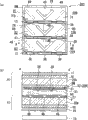
Secondly, according to Fig. 3 the pixel formation of the liquid crystal indicator 100 of this example is described.The pixel that the mode chart of Fig. 3 (a) shows liquid crystal indicator 100 constitutes, and the plane that mainly shows pixel electrode 31 constitutes, and the mode chart of Fig. 3 (b) shows the A-A ' section of Fig. 3 (a).The liquid crystal indicator 100 of this example has it and constitutes the some zone (D1, D2, D3) that possesses pixel electrode 31.In this some zone, shown in Fig. 3 (a), set dyed layer of the same colour within 3 primary colors accordingly with a some zone.Form the pixel that contains each dyed layer 22B (blueness), 22G (green), 22R (redness) with 3 some zones (D1, D2, D3), become the formation that shows for available each pixel unit.
Shown in Fig. 3 (b), the liquid crystal indicator 100 of this example, between the infrabasal plate (subtend substrate) 10 of upper substrate (device substrate) 25 and subtend configuration with it, seize initial orientation state on both sides by the arms and take vertical orientated liquid crystal, in other words, seize the liquid crystal layer 50 that constitutes for negative liquid crystal material by dielectric anisotropy on both sides by the arms.That is, the liquid crystal indicator 100 of this example is the transmission liquid crystal display device that adopts vertical alignment mode.
Secondly, in upper substrate 25 1 sides,, be provided with color filter 22 (in Fig. 3 (b), being red colored layer 22R) in the base main body 25A top (liquid crystal layer one side of base main body 25A) that the translucent material by glass or quartz etc. constitutes.Here, the periphery of dyed layer 22R is fenced up by the black matrix" BM that is made of crome metal etc., forms the border (referring to Fig. 3 (a)) of each region D 1, D2, D3 with this black matrix" BM.In addition, be formed with rectangular pixel electrode 31 that the nesa coating by ITO etc. constitutes and in color filter 22 tops by the alignment films 33 of the same vertical orientated processing of having carried out of constituting such as polyimide and infrabasal plate 10.In addition, though details will be told about in the back, also be formed with it and constitute outstanding projection 28 to liquid crystal layer 50 on the inner face side plan view rectangular shape of upper substrate 25 ground.
In addition, on the outside of infrabasal plate 10 side (sides different) with the face of seizing liquid crystal layer 50 on both sides by the arms, form polarizer 18 and polaroid 19, on the side of the outside of upper substrate 25, also form polarizer 16 and polaroid 17, in substrate inner face side (liquid crystal layer 50 1 sides) but on constitute the incident circularly polarized light, these polarizers 18 and polaroid 19, polarizer 16 and polaroid 17 constitute circular polarizing disk respectively.Polaroid 17 (19) is made the formation of the linear polarization transmittance that only makes the polarizing axis that possesses predetermined direction, as polarizer 16 (18) employings are λ/4 polarizers, as such circular polarizing disk, in addition, can also use the formation polarizer (broadband circular polarizing disk) that λ/2 polarizers and λ/4 polarizers are combined, in this case, the result just becomes to becoming black display and is netrual colour more.In addition, also can use the polarizer of the formation that a polaroid and λ/2 polarizers and λ/4 polarizers and C plate (polarizer that has optical axis at film thickness direction) combine, the result just becomes to realizing further wide visual field angleization.In addition, the arranged outside at the polaroid 19 that forms on infrabasal plate 10 has the backlight 15 that shows the light source of usefulness as transmission.
Here, the liquid crystal indicator 100 of this example is the liquid crystal indicator that constitutes the vertical alignment mode of liquid crystal layer 50 with dielectric anisotropy for negative liquid crystal material as mentioned above.Therefore, because liquid crystal molecule can be toppled over because of electric field applies under initial orientation state, so if the liquid crystal molecule of for the real estate standing upright does not move what brains (if not giving pre-tilt angle) then the toppling direction of just impossible control liquid crystal molecule, will make that the demonstration that produces light omission etc. is bad because of the disorder that produces orientation, make display characteristic decline.For this reason, when adopting vertical alignment mode, the control of the direction of orientation of the liquid crystal molecule when electric field applies just becomes and is important key element.
So, in the liquid crystal indicator 100 of this example, become such formation: adopt the face of seizing on both sides by the arms to liquid crystal layer 50 to form the way of the projection (male member or the face convex shape of seizing on both sides by the arms are given means) that the dielectric by acrylic resin etc. constitutes, give the pre-tilt corresponding to liquid crystal molecule with its convex shape, on the other hand, adopt and form the way in the slit of an electrode incised notch part, and the electrode of subtend between produce oblique electric field, give the pre-tilt corresponding with this oblique electric field.Specifically, as shown in Figure 3, become such formation: it constitutes the slit 49 (dotting in Fig. 3 (a)) of a part of strip of self or rectangle shape ground incised notch in formation on the common electrode 9, on the other hand, formation constitutes the projection 28 that constitutes to the outstanding dielectric of liquid crystal inner face from pixel electrode 31 with it on upper substrate 25 inner faces.
Particularly in this example, form on the position that is differing from one another setting in the slit 49 that forms on the common electrode 9 and the projection 28 that forming on the inner face of upper substrate 25 to making, that is, make projection 28 plane earths be positioned at 49,49 in slit adjacent one another are within a plurality of slits 49.Consequently, the toppling direction that is difficult to form liquid crystal molecule in slit adjacent one another are between 49,49 or adjacent projection becomes and is discontinuous zone, thus can efficient more the highland prevent or suppress the generation of orientation disorder.
In addition, in this example, become such formation: in the zone of the projection 28 of the direction of orientation that has formed restriction or control liquid crystal molecule, on pixel electrode 31, form opening, promptly on the inner face side of projection 28 and outside one side, do not have electrode.Consequently, because the direction that influences liquid crystal toppling direction and line of electric force of projection 28 will become to contrary direction,, can carry out the orientation limitations of more stable liquid crystal molecule so the toppling direction of liquid crystal is easy to fix.In addition, even if directly form the formation of projection 28 in pixel electrode 31 tops, also can limit the direction of orientation of liquid crystal molecule.
If adopt such formation, remove liquid crystal molecule under original state, present vertical orientated outside, also have and the corresponding pre-tilt of oblique electric field based on the formation in the convex form of projection 28 and slit 49.Consequently can provide and the restriction of the toppling direction of liquid crystal molecule or to control on the predetermined direction, be difficult to produce orientation disorder, can avoid the demonstration of light omission etc. bad, inhomogeneous etc. the demonstration that can suppress after image or dirt shape is bad, and the liquid crystal indicator of visual field angular width.
On the other hand, in the liquid crystal indicator 100 of this example, shown in Fig. 3 (a), pixel electrode 31 is supplied with the signal wire of signal, here be to supply with sweep trace 13 tops of sweep signals to pixel electrode 31, the projection 38 that the dielectric by acrylic resin etc. constitutes is set by TFD.Specifically, shown in the sectional view of Fig. 8, the form of getting up is crossed over this sweep trace 13 and pixel electrode 31 ground form so that sweep trace 13 planarityes ground is covered, and is constructed such that and the part of the outer rim of pixel electrode 31 is covered (also referring to Fig. 2).
Here; for example under the situation that does not form projection 38; pixel electrode 31 is supplied with the sweep trace 13 of signal; sometimes can and pixel electrode 31 between produce transverse electric field; when this transverse electric field had taken place, liquid crystal molecule just usually can present and the different performance of orientation based on the electric field between common pixel electrode 31 and common electrode 9.Produced owing to such transverse electric field to the situation of usually different direction orientation under, carry out the orientation limitations of liquid crystal molecule even if adopt the way that in pixel, forms projection 28 or slit 49 as mentioned above like that, particularly in the pixel neighboring area, the orientation that also exists liquid crystal molecule produces disorder, causes the possibility of the reduction of display characteristic.
So, in this example, as Fig. 3 (a) and shown in Figure 8, employing forms the projection 38 (male members that are made of dielectric in sweep trace 13 tops, or the face convex shape of seizing on both sides by the arms is given means) way, just can get up electric shield between sweep trace 13 and the pixel electrode 31, prevent or suppress the generation of above-mentioned transverse electric field.In addition, even if supposition has taken place under the situation of transverse electric field, also can make the influence that is not subjected to transverse electric field by means of orientation limitations power along the convex shape of this projection 38, promptly, by means of the also big orientation limitations power of the influence that affacts the ratio transverse electric field on the liquid crystal molecule, just can be restricted to the liquid crystal molecular orientation of the formation area peripheral edge of sweep trace 13 on the predetermined direction based on the shape of projection 38.Consequently, can provide particularly near the zone that has formed sweep trace 13, can limit and control the toppling direction of liquid crystal molecule, be difficult to produce the disorder of orientation, can avoid the demonstration of light omission etc. bad, inhomogeneous etc. the demonstration that can suppress after image or dirt shape is bad, and the liquid crystal indicator of visual field angular width.
In addition, the projection of using in this example 28,38 can constitute with same material, and available same technology forms.In addition, projection 28,38, the face of seizing on both sides by the arms the convex shape that plays a part convex shape is given the face of seizing on both sides by the arms of liquid crystal layer 50 is given means, specifically, it constitutes possesses 50 dip plane of giving prominence to the mountain shape of predetermined height (for example 0.05 micron to 1.5 microns is said about 0.07 micron to 0.2 micron ideally) just from the substrate inner face to liquid crystal layer.
In addition, the convex shape of projection 28,38, its longitudinal profile shape forms symmetrical substantially shape.For example, have substantially triangular shaped projection 28,38 if constitute the longitudinal profile, then the result becomes to the core (top) with this projection when the lqiuid crystal molecule tipping is that topple on contrary respectively direction ground, boundary, can obtain wide field angle characteristic.In order to obtain so wide field angle characteristic, projection 28,38, it is desirable to remove triangular shaped outside, make its longitudinal profile shape constitute trapezoidal shape or half-oval shaped.
Example 2
Below, the limit describes example 2 of the present invention referring to the accompanying drawing limit.
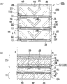
Fig. 4 shows planimetric map and sectional view to the liquid crystal indicator 200 of example 2, is the mode chart that is equivalent to Fig. 3 of example 1.The basic comprising of the liquid crystal indicator of this example and example 1 are same, mainly are that to carry out the formation position in the dielectric projection of orientation limitations of liquid crystal molecule or electrode slit different.Therefore, in Fig. 4, give same label and omit detailed explanation for the inscape that those and Fig. 3 are common.
As shown in Figure 4, in the liquid crystal indicator 200 of example 2, on the pixel electrode 31 that forms on the inner face of upper substrate 25, slit 48 is being set, on the inner face of infrabasal plate 10, is forming projection 29.In this case, slit 48 also be adopt the part of pixel electrode 31 partly the way plan view of incised notch be into strips or rectangular shape formed opening, in addition, projection 29 is that the male member (the face convex shape of seizing on both sides by the arms is given means) that the dielectric by acrylic resin etc. constitutes is formed strip or rectangular shape, possesses the shape that the longitudinal profile is shaped as triangular shaped substantially chevron.In this case, also can give corresponding with the convex shape of projection 29 pre-tilt for liquid crystal molecule, on the other hand, also can give with based on the corresponding pre-tilt of the oblique electric field in slit 48.
In addition, will be the slit 48 that on pixel electrode 31, forms, form on the position that is differing from one another with setting in the projection 29 that forms on the inner face of infrabasal plate 10, promptly set to making that 48,48 plane earths set projection 29 in adjacent slit within a plurality of slits 48 to making.Thus, to become be the generation of the such discontinuity zone (orientation disorder) of contrary direction to projection adjacent one another are or the slit toppling direction of having eliminated liquid crystal molecule to each other.In addition, also to constitute, make common electrode 31 form opening, promptly not have electrode in the inboard of projection 29 in projection 29 tops of the direction of orientation of restriction or control liquid crystal molecule.
Employing sets the way in such projection 29 and slit 48, the result just become for remove liquid crystal molecule present under the original state vertical orientated outside, also have and the corresponding pre-tilt of oblique electric field based on the formation in the convex shape of projection 29 and slit 48.Consequently, can provide and the toppling direction of liquid crystal molecule restriction or to control on the predetermined direction, be difficult to produce the disorder of orientation, can avoid the demonstration of light omission etc. bad, inhomogeneous etc. the demonstration that can suppress after image or dirt shape is bad, and the liquid crystal indicator of visual field angular width.
On the other hand, shown in Fig. 4 (a), pixel electrode 31 is supplied with the signal wire of signal, here be to supply with the sweep trace 13 planarityes ground position overlapped of sweep signals to pixel electrode 31 by TFD, promptly be that planarity ground covers the position of getting up to sweep trace 13, be again on the inner face of substrate (infrabasal plate 10) of a side different, set the projection 39 that the dielectric by acrylic resin etc. constitutes with the substrate that has formed this sweep trace 13 (upper substrate 25).Specifically, as shown in figure 10, form projection 39 in infrabasal plate 10 tops sweep trace 31 planarityes ground is covered the form of getting up.In addition, the part of the outer rim that is constructed such that pixel electrode 31 of projection 39 is also carried out overlapping.
As mentioned above; pixel electrode 31 is supplied with the sweep trace 13 of signal; sometimes can and pixel electrode 31 between produce transverse electric field; when this transverse electric field had taken place, liquid crystal molecule just usually can present and the different performance of orientation based on the electric field between common pixel electrode 31 and common electrode 9.Produced owing to such transverse electric field to the situation of usually different direction orientation under, carry out the orientation limitations of liquid crystal molecule even if adopt the way that in pixel, forms projection 29 or slit 48 as mentioned above like that, particularly in the pixel neighboring area, the orientation that also exists liquid crystal molecule produces disorder, causes the possibility of the reduction of display characteristic.
So, in this example, as Fig. 4 (a) and shown in Figure 10, employing is being to carry out the plane position overlapped with sweep trace 13, be again to form the projection 39 (male members that constitute by dielectric in substrate (infrabasal plate a 10) side different with the substrate that has formed this sweep trace 13 (upper substrate 25), or the face convex shape of seizing on both sides by the arms is given means) way, even if supposition has taken place under the situation of transverse electric field, also can make the influence that is not subjected to transverse electric field by means of orientation limitations power along the convex shape of this projection 39, promptly, by means of the also big orientation limitations power of the influence that affacts the ratio transverse electric field on the liquid crystal molecule, just can be restricted to the liquid crystal molecular orientation of the formation area peripheral edge of sweep trace 13 on the predetermined direction based on the shape of projection 39.Consequently, can provide particularly near the zone that has formed sweep trace 13, can limit and control the toppling direction of liquid crystal molecule, be difficult to produce the disorder of orientation, can avoid the demonstration of light omission etc. bad, inhomogeneous etc. the demonstration that can suppress after image or dirt shape is bad, and the liquid crystal indicator of visual field angular width.
In addition, the projection 29,39 that forms at infrabasal plate 10 inner faces can constitute with same material, and available same technology forms.In addition, projection 29,39, the face of seizing on both sides by the arms the convex shape that plays a part convex shape is given the face of seizing on both sides by the arms of liquid crystal layer 50 is given means, specifically, it constitutes the dip plane that possesses the mountain shape of the 50 outstanding height of being scheduled to (for example 0.05 micron to 1.5 microns is said about 0.07 micron to 0.2 micron ideally) from the substrate inner face to liquid crystal layer.
In addition, the convex shape of projection 29,39, its longitudinal profile shape forms symmetrical substantially shape.For example, if constitute the length direction projection 29,39 that the longitudinal profile has triangular shaped chevron substantially, then the result becomes to the core (top) with this projection when the lqiuid crystal molecule tipping is that topple on contrary respectively direction ground, border, can obtain wide field angle characteristic.In order to obtain so wide field angle characteristic, projection 29,39, it is desirable to remove triangular shaped outside, make its longitudinal profile shape constitute trapezoidal shape or half-oval shaped.
Example 3
Below, the limit describes example 3 of the present invention referring to the accompanying drawing limit.
Fig. 5 shows planimetric map and sectional view to the liquid crystal indicator 300 of example 3, is the mode chart that is equivalent to Fig. 3 of example 1.The basic comprising of the liquid crystal indicator of this example and example 1 are same, mainly are that the formation of the projection that forms in the sweep trace top is different.Therefore, in Fig. 5, give same label and omit detailed explanation for the inscape that those and Fig. 3 are common.
Shown in Fig. 5 (a), in the liquid crystal indicator 300 of example 3, in a pixel, supplying with sweep trace 13 tops of sweep signals to pixel electrode 31 by TFD, be formed with a plurality of projections 38 that constitute by the dielectric of acrylic resin etc.Specifically, be formed with the projection 38 of a plurality of point-like or rectangular shape on the borderline region in a some region D 1, D2, D3 or in each region D 1, D2, D3.
In this case, same with example 1, also can get up electric shield between sweep trace 13 and the pixel electrode 31, prevent or suppress the generation of transverse electric field between above-mentioned sweep trace 13 and the pixel electrode 31.In addition, even if supposition has taken place under the situation of transverse electric field, can not be subjected to the influence of transverse electric field by means of orientation limitations power along the convex shape of this projection 38 yet, promptly, by means of the also big orientation limitations power of the influence that affacts the ratio transverse electric field on the liquid crystal molecule, just can be restricted to the liquid crystal molecular orientation of the formation area peripheral edge of sweep trace 13 on the predetermined direction based on the shape of projection 38.Consequently, can provide particularly near the zone that has formed sweep trace 13, can limit or control the toppling direction of liquid crystal molecule, be difficult to produce the disorder of orientation, can avoid the demonstration of light omission etc. bad, inhomogeneous etc. the demonstration that can suppress after image or dirt shape is bad, and the liquid crystal indicator of visual field angular width.
In addition, on upper substrate 25 inner faces, form projection 28,38 can constitute with same material, available same technology forms.In addition, projection 28,38, the face of seizing on both sides by the arms the convex shape that plays a part convex shape is given the face of seizing on both sides by the arms of liquid crystal layer 50 is given means, specifically, it constitutes the dip plane that possesses the mountain shape of the 50 outstanding height of being scheduled to (for example 0.05 micron to 1.5 microns is said about 0.07 micron to 0.2 micron ideally) from the substrate inner face to liquid crystal layer.In addition, the convex shape of projection 28,38, same with example 1, its longitudinal profile shape forms symmetrical substantially shape.
Example 4
Below, the limit describes example 4 of the present invention referring to the accompanying drawing limit.
Fig. 6 shows planimetric map and sectional view to the liquid crystal indicator 400 of example 4, is the mode chart that is equivalent to Fig. 3 of example 1.The basic comprising of the liquid crystal indicator of this example and example 1 are same, mainly are that to carry out the formation in the projection of orientation limitations of liquid crystal molecule or electrode slit different.Therefore, in Fig. 6, give same label and omit detailed explanation for the inscape that those and Fig. 3 are common.
As shown in Figure 6, in the liquid crystal indicator 400 of example 4, on the pixel electrode 31 that forms on the inner face of upper substrate 25, slit 48 is being set, on the inner face of infrabasal plate 10 for common electrode 9, also form slit 49.In this case, slit 48,49 also be adopt the part of each electrode 31,9 partly incised notch the way plan view for into strips or rectangular shape ground formed opening, can give and based on the corresponding pre-tilt of oblique electric field of slit formation liquid crystal molecule.In addition, will be the slit 48 that on pixel electrode 31, forms, form on the position that is differing from one another with setting in the slit 49 that forms on the common electrode 9, promptly set to making the 49 planarityes ground, slit of subtend one side between slit adjacent one another are within a plurality of slits 48 48,48 to making.By means of this, become the generation of the discontinuity zone that is that contrary direction is such with regard to the toppling direction of having eliminated liquid crystal molecule between adjacent slits.
On the other hand, shown in Fig. 6 (a), setting the projection 38 that the dielectric by acrylic resin etc. constitutes to the top that pixel electrode 31 is supplied with the sweep trace 13 of sweep signals by TFD.In this case, by means of projection 38, also can prevent or be suppressed at the generation of the transverse electric field between sweep trace 13 and the pixel electrode 31, even if supposition has taken place under the situation of transverse electric field, can not be subjected to the influence of transverse electric field by means of orientation limitations power along the convex shape of this projection 38 yet, promptly, by means of the also big orientation limitations power of the influence that affacts the ratio transverse electric field on the liquid crystal molecule, just can be restricted to the liquid crystal molecular orientation of the formation area peripheral edge of sweep trace 13 on the predetermined direction based on the shape of projection 38.
In addition, in this example,, only just carry out the orientation limitations of liquid crystal molecule at place, electrode slit owing to do not form projection in pixel inside.Though so formed projection 38 with manufacturing process independently,, also can with the liner (not drawing) of the bed thickness of restriction liquid crystal layer 50 with same operation formation.That is, in the liquid crystal indicator of light liner that has formed so-called shellfish column on the substrate inner face and so on, the projection 38 that forms sweep trace 13 tops with the formation operation of this liner simultaneously is possible.In addition, in the means of the direction of orientation that can constitute projection 38 the restriction liquid crystal molecule, can also make it to constitute the means of restriction liquid crystal bed thickness, promptly can also constitute the projection 38 of the function that has both both sides.
Example 5
Below, the limit describes example 5 of the present invention referring to the accompanying drawing limit.
Fig. 7 shows planimetric map and sectional view to the liquid crystal indicator 500 of example 5, is the mode chart that is equivalent to Fig. 3 of example 1.The basic comprising of the liquid crystal indicator of this example and example 1 are same, and different is that the common electrode 9 usefulness metallic reflective coatings that form on infrabasal plate 10 inner faces constitute this point.Therefore, in Fig. 7, give same label and omit detailed explanation for the inscape that those and Fig. 3 are common.
As shown in Figure 7, in the liquid crystal indicator 500 of example 5, be formed in the common electrode 90 that forms on the inner face of infrabasal plate 10, this common electrode (reflectance coating) 90 is formed slit 49 with reflexive metal film.In addition, in the outside of infrabasal plate 10 side, do not form polarizer, polaroid, backlight etc., can adopt the way of the outer light of the sunshine of going into to shine from outside one side of upper substrate 25, illumination light etc. to show with common electrode (reflectance coating) 90 reflection.In other words, liquid crystal indicator 500 of the present invention is the reflective liquid crystal indicators that adopt vertical alignment mode.
In the reflective LCD device that adopts such vertical alignment mode, also become such formation: adopt when on common electrode (reflectance coating) 90, forming slit 49, inner face side at upper substrate 25 forms projection 28, carry out the orientation limitations of liquid crystal molecule in the pixel, and also form the way of projection 38 in sweep trace 13 tops, the liquid crystal molecule of pixel neighboring area is also carried out orientation limitations.
In this case, slit 49 also is that to adopt partly the way of the part of incised notch common electrode (reflectance coating) 90 to form rectangular or oblong openings portion, makes to give and the corresponding pre-tilt of oblique electric field based on slit formation liquid crystal molecule.In addition, also become such formation: constituting to liquid crystal layer 50 of projection 28 highlights, with its convex shape accordingly, promptly limit the toppling direction of liquid crystal molecule accordingly with the dip plane of projection 28.In addition, the slit 49 that on common electrode (reflectance coating) 90, forms, with set to the position that makes it differing from one another in the projection 28 that forms on the inner face of upper substrate 25 on form, promptly set for the projection 28 planarityes ground that makes subtend one side between slit adjacent one another are within a plurality of slits 49 49,49.By means of this, between adjacent slits, become the generation of the discontinuity zone that is that contrary direction is such with regard to the toppling direction of having eliminated liquid crystal molecule.
In addition, the projection 38 that forms in sweep trace 13 tops is that the dielectric of available acrylic resin etc. constitutes, and it constitutes the interior projection that highlights towards liquid crystal layer 50 from upper substrate 25, and, electric shield between pixel electrode 31 and the sweep trace 13 get up.In addition, constituting of projection 38 removed outside the electric shielding effect, can also with its shape accordingly, promptly limit the toppling direction of liquid crystal molecule accordingly with the dip plane of self.Therefore, adopt the way that forms projection 38, just can prevent or suppress the generation of the transverse electric field between pixel electrode 31 and the sweep trace 13, even if transverse electric field has taken place in supposition between the two, by means of high orientation limitations power based on its convex shape, also can be with the direction of orientation of the form restriction liquid crystal molecule of the influence of offsetting transverse electric field.
In sweep trace 13 tops shown in above such example 1 to 5 or overlap onto the projection (38,39) that forms on the sweep trace 13, can be according to suitable formation position or the shape selected of direction of wanting to make lqiuid crystal molecule tipping, as for projection in the pixel 28,29 and electrode slit 48,49, also can select it to form the position according to the toppling direction of liquid crystal molecule is suitable.For example, as shown in Figure 9, employing forms the sweep trace 13 that makes being provided in 31,31 of pixel electrodes adjacent one another are to projection 38 and covers the way of getting up, though can prevent or suppress the generation of transverse electric field, carry out the orientation limitations of liquid crystal molecule simultaneously according to its convex shape, still, as shown in Figure 8, employing forms projection 38 and makes the way that the part of the outer rim of each pixel electrode 31,31 is covered, and can effect suppresses the generation of transverse electric field more well.
In addition, as shown in Figure 9, carry out under the overlapping situation even if projection 39 is formed the sweep trace 13 that makes and be provided between the different pixel electrode 31,31 in substrate 10A one side different with the substrate 25A that has formed sweep trace 13, it also is desirable making it to carry out overlapping with the form that the part of the outer rim of pixel electrode adjacent one another are 31,31 is covered.In this case, have benefited from the orientation limitations power based on convex shape, the influence of further lowering the transverse electric field between pixel electrode 31 and the sweep trace 13 is possible.
In addition, as shown in figure 11, as long as near formation projection sweep trace 13 at least, also can between pixel electrode 31 and sweep trace 13, form projection 38a and need not cover sweep trace 13 tops.In addition, subtend one side at sweep trace 13 forms under the situation of projection, also can become is being between pixel electrode 31 and the sweep trace 13, is again to form the formation of projection 39a on the substrate with the substrate subtend that has formed sweep trace 13, and is not that must overlap onto can not on the sweep trace 13.
Example 6
Below, the limit describes example 6 of the present invention referring to the accompanying drawing limit.
Figure 12 shows planimetric map and sectional view to the liquid crystal indicator 600 of example 6, is the mode chart that is equivalent to Fig. 3 of example 1.The basic comprising of the liquid crystal indicator of this example and example 1 are same, and different is to form reflectance coating on ground, infrabasal plate 10 inner face tops, make can carry out the transmission demonstration and reflect showing this both sides' this point.Therefore, in Figure 12, give same label and omit detailed explanation for the inscape that those and Fig. 3 are common.
As shown in figure 12, the liquid crystal indicator 600 of this example, inner face side at infrabasal plate 10 partly forms reflectance coating 20, make and in the formation zone of this reflectance coating 20, to reflect demonstration, in the non-formation zone (open area of reflectance coating 20) of this reflectance coating 20, carry out transmission and show.In other words, the liquid crystal indicator 600 of this example is the liquid crystal indicator that adopts the Transflective of vertical alignment mode.
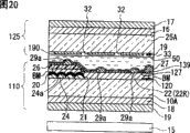
At first, shown in Figure 12 (b), the liquid crystal indicator 600 of this example, same with the liquid crystal indicator 100 of example 1, between the infrabasal plate (subtend substrate) 10 of upper substrate (device substrate) 25 and subtend configuration with it, seize initial orientation state on both sides by the arms and take vertical orientated liquid crystal, in other words the liquid crystal layer 50 that constitutes for negative liquid crystal material by dielectric anisotropy.
Exist dielectric film 24 ground in the middle of the constituting on the surface of the base main body 10A that the translucent material by quartz, glass etc. constitutes of infrabasal plate 10 and partly form the reflectance coating 20 that the high metal film of reflectivity by aluminium, silver etc. constitutes.Here, the formation zone of reflectance coating 20 just becomes and is reflective display region territory R, and the non-formation zone of reflectance coating 20 just becomes in the opening portion 21 of reflectance coating 20 in other words and is transmission viewing area T.
The constituting of dielectric film 24 that forms in base main body 10A top possesses concaveconvex shape 24a in its surface, and the surface of reflectance coating 20 is then because of imitating this concaveconvex shape to have concaveconvex shape.Because reflected light can carry out scattering by means of such concaveconvex shape, so can prevent that the reflection demonstration that obtains wide visual field angle becomes possibility from the mirroring of outside.In addition, possess the dielectric film 24 of such concaveconvex shape 24a, for example can adopt to make the resin photoresist graphical, the way that applies other one deck resin above that obtains.In addition, also can heat-treat to adjust shape the resin photoresist after graphical.
In addition, in reflectance coating 20 tops that are positioned at reflective display region territory R, with the base main body 10A top that is positioned at transmission viewing area T, be provided with the color filter 22 (in Figure 12 (b), being red colored layer 22R) of crossing over these reflective display region territory R and the formation of T ground, transmission viewing area.Here the periphery of dyed layer 22R has used the black matrix" BM that is made of crome metal etc. to fence up, has formed the border (referring to Figure 12 (a)) of each region D 1, D2, D3 by means of black matrix" BM.
Have again,, on the position corresponding, be formed with dielectric film 26 with reflective display region territory R in color filter 22 tops.In other words, exist the top that color filter 22 ground are positioned at reflectance coating 20 in the middle of making and like that optionally form dielectric film 26, the formation that is accompanied by this dielectric film 26 makes that the thickness of liquid crystal layer 50 is different in reflective display region territory R and transmission viewing area T.Dielectric film 26 for example is made of the organic membrane of acrylic resin of about 0.5 micron to 2.5 microns of thickness etc., and the boundary vicinity between reflective display region territory R and transmission viewing area T possesses such dip plane that self thickness changes continuously.Do not exist the thickness of liquid crystal layer 50 of the part of dielectric film 26 to be made about about 1 micron to 5 microns, it is only about half of that the thickness of the liquid crystal layer 50 among the R of reflective display region territory then is made the thickness of the liquid crystal layer 50 among the T of transmission viewing area.As mentioned above, dielectric film 26 plays a part to make the R liquid crystal bed thickness different with the bed thickness of the liquid crystal layer 50 of transmission viewing area T in reflective display region territory adjust layer (liquid crystal bed thickness key-course) by means of the thickness of self.
In addition, in the plan view central authorities substantially of the dielectric film 26 that in the R of reflective display region territory, forms, form it and constitute projection (male member) 29a that highlights to liquid crystal layer 50 inside from the surface of this dielectric film 26.This projection 29a, constitute by the dielectric of acrylic resin etc., the convex shape that plays a part the convex shape that possesses the dip plane is given the face of seizing on both sides by the arms of liquid crystal layer 50 is given means, specifically, it constitutes from the outstanding predetermined height (for example 0.05 micron to 1.5 microns is said about 0.07 micron to 0.2 micron ideally) in the surface of dielectric film 26.
On the other hand, in color filter 22 tops, on the position corresponding, be formed with it and constitute projection (male member) 29a that highlights to liquid crystal layer 50 inside from the surface of this color filter 22 with transmission viewing area T.This projection 29a, similarly constitute with above-mentioned reflective display region territory R by the dielectric of acrylic resin etc., the convex shape that plays a part the convex shape that possesses the dip plane is given the face of seizing on both sides by the arms of liquid crystal layer 50 is given means, specifically, it constitutes from the outstanding predetermined height (for example 0.05 micron to 1.5 microns is said about 0.07 micron to 0.2 micron ideally) in the surface of dielectric film 26.In other words, the projection 29a that forms on reflective display region territory R and transmission viewing area T forms with same manufacturing process respectively, constitutes as the dielectric that the organic membrane of the acrylic resin of same material etc. constitutes with this.
In addition,, form the banded common electrode 9 that constitutes by indium tin oxide (below, be abbreviated as ITO), form the alignment films 27 that constitutes by polyimide etc. in common electrode 9 tops in color filter 22 tops that comprise dielectric film 26 and projection 29a.Alignment films 27 is films that liquid crystal molecule is worked as the vertical alignment layer that vertically is orientated for face, implements the orientation process of friction etc.In addition, common electrode 9 is formed in the ribbon that extends on the paper vertical direction in Figure 12, all can be used as shared electrode on each in the some zone that forms side by side and constitute on this paper vertical direction.In addition, in this example, though form reflectance coating 20 and common electrode 9 dividually,, in the R of reflective display region territory, also can be used as the reflectance coating that constitutes by metal film the part of common electrode.In addition, also become on the inner face of projection 29a and outside and do not form common electrode 9, in the opening portion of common electrode 9, form the formation of projection 29a.
Secondly, on upper substrate 25 1 sides, on the base main body 25A (liquid crystal layer one side of base main body 25A) that the translucent material by glass or quartz etc. constitutes, be formed with rectangular pixel electrode 31 that the nesa coating by ITO etc. constitutes and by the alignment films 33 of the same vertical orientated processing of having carried out of constituting such as polyimide and infrabasal plate 10.In addition, being formed with it on pixel electrode 31 constitutes partly the slit 32 of a part of incised notch of self.
In addition, on the side of the outside of infrabasal plate 10, be formed with polarizer 18 and polaroid 19, a side also is formed with polarizer 16 and polaroid 17 in the outside of upper substrate 25, in substrate inner face side (liquid crystal layer 50 1 sides) but on constitute the incident circularly polarized light, these polarizers 18 and polaroid 19, polarizer 16 and polaroid 17 constitute circularly polarizing plate respectively.
Here, in the liquid crystal indicator 600 of this example, for the liquid crystal molecule to liquid crystal layer 50 carries out orientation limitations, promptly for in original state, being in vertical orientated liquid crystal molecule, be limited in the toppling direction when being applied with voltage between electrode, on the inner face side (liquid crystal layer one side) of infrabasal plate 10, be formed with the projection 29a that constitutes by dielectric.Specifically, in the example of Figure 12, on the inner face side (liquid crystal layer one side) of the color filter 22 that forms on the infrabasal plate 10, on reflective display region territory R and transmission viewing area these both sides of T, be formed with projection 29a to liquid crystal layer 50 inner shapes of giving prominence to, possess the shape of the frustum of a cone substantially.
The projection 29a that forms like this is along the toppling direction of its convex shape (particularly dip plane) restriction liquid crystal molecule.In other words, though be in vertical orientated liquid crystal molecule under the voltage original state as yet to applying between electrode, after being applied with voltage, will topple over to the direction that intersects with its direction of an electric field, but, if adopt this example, the toppling direction of the liquid crystal molecule when then this voltage being applied is restricted to along the dip plane of projection 29a.
In addition, projection 29a, as long as be constructed such that the surface (dip plane) that makes its convex shape is for the lucky angle that tilts to be scheduled to of the vertical orientated direction of liquid crystal molecule, for example, it is desirable to coniform or oval taper perhaps polygonal taper, circular cone shape, oval frustum, hemispherical formation.In addition, as for the dip plane of projection 29a, it is desirable to its allowable angle of inclination and be 2 and spend to 20 degree.Pitch angle under so-called this situation refers to the angle that the dip plane constituted of real estate (interarea) Yu the projection 29a of substrate 10A, and has under the curved surface situation at projection 29a, refers to and this curved surface abutted surface and real estate angulation.Under the situation of allowable angle of inclination less than 2 degree in this case, sometimes just be difficult to limit the toppling direction of liquid crystal molecule, and surpassed when allowable angle of inclination under the situation of 20 degree, then sometimes can produce light omission etc., the shortcoming of generation contrast reduction etc. from this part.
On the other hand,, go up on the pixel electrode 31 that forms, formed slit 32 in inner face side (liquid crystal layer one side) at upper substrate 10 for the liquid crystal molecule to liquid crystal layer 50 carries out orientation limitations.Promptly adopt the way that on pixel electrode 31, forms slit 32, the result just become for and the common electrode 9 of subtend between can produce oblique electric field along the formation position in this slit 32, by means of this oblique electric field, the toppling direction of the liquid crystal molecule when deboost applies.
In addition, since on pixel electrode 31, formed slit 32, this pixel electrode 31, shown in Figure 12 (a), just be divided into octagonal substantially sub-point (island part) 31a, 31b, 31c, each height point (island part) 31a, 31b, 31c couple together by means of linking portion 59.In addition, near the center substantially that is sub-point (island part) 31a, 31b, 31c, be again to form projection 29a on substrate one side of its subtend, consequently become for liquid crystal molecule be that to all the winds topple at the center with this projection 29a, in other words, in this example, become to each height point (island part) 31a, 31b, 31c having been carried out the formation of cutting apart of orientation.
Have, in the liquid crystal indicator 600 of this example, sweep trace 13 tops that form on the inner face of upper substrate 25 are formed with the projection 38 that is made of dielectric again.Specifically, form these sweep trace 13 part ground are covered the form of getting up along sweep trace 13.Adopt and form the projection 38 (male members that constitute by dielectric like this in sweep trace 13 tops, or the face convex shape of seizing on both sides by the arms is given means) way, just can get up electric shield between sweep trace 13 and the pixel electrode 31, prevent or suppress the generation of above-mentioned transverse electric field.In addition, even if supposition has taken place under the situation of transverse electric field, can not be subjected to the influence of transverse electric field by means of orientation limitations power along the convex shape of this projection 38 yet, promptly, by means of the also big orientation limitations power of the influence that affacts the ratio transverse electric field on the liquid crystal molecule, just can be restricted to the liquid crystal molecular orientation of the formation area peripheral edge of sweep trace 13 on the predetermined direction based on the shape of projection 38.
In addition, the convex shape of projection 38, its longitudinal profile shape forms symmetrical substantially shape.For example, have substantially triangular shaped long shape projection 38 if constitute the longitudinal profile, then the result becomes to the core (top) with this projection when the lqiuid crystal molecule tipping is that topple on contrary respectively direction ground, boundary, can obtain wide field angle characteristic.In order to obtain so wide field angle characteristic, projection 38, it is desirable to remove triangular shaped outside, make its longitudinal profile shape constitute trapezoidal shape or half-oval shaped.
In addition, though projection 38 is with part ground sweep trace 13 to be covered the form of getting up to form,, particularly in this example, shown in Figure 12 (a), on the pixel electrode 31 of octagonal shape substantially and sweep trace 13 immediate positions, be formed with projection 38.That is, on the approaching position of pixel electrode 31 and sweep trace 13, owing to be easy to produce above-mentioned transverse electric field, so adopt the way of formation projection 38 on this position, the orientation limitations of liquid crystal molecule just will become to the most effective.
If adopt the liquid crystal indicator 600 of this example that possesses such formation, then the result just becomes to realizing following desirable effect and effect.
At first, in the liquid crystal indicator 600 of this example, owing to making substantially half of thickness that can be reduced to the thickness of the liquid crystal layer 50 of reflective display region territory R the liquid crystal layer 50 of transmission viewing area T because of reflective display region territory R optionally being provided with dielectric film 26, so participation reflection light path that shows and the light path that participates in the transmission demonstration are equated substantially, by means of this, realized the raising of contrast.
In addition, in general, if be applied with voltage for liquid crystal molecule with negative dielectric anisotropy in the vertical alignment layer top orientation of not implementing friction treatment, because the toppling direction of liquid crystal without limits, so liquid crystal molecule just topples over to chaotic direction, the result just become for meeting produce be orientated bad.But, in this example, because means as the toppling direction that limits liquid crystal molecule, on the inner face of infrabasal plate 10, formed projection 29a, on the pixel electrode 31 that forms on the inner face of upper substrate 25, forming slit 32, so will produce orientation limitations by dip plane (shape dip plane, the mountain) generation of projection 29a, with the orientation limitations that is produced by 32 the oblique electric field along the slit, the result applies the direction of toppling over regard to becoming to what may be limited to liquid crystal molecule vertical orientated under the original state because of voltage.Consequently, because based on being suppressed of the bad orientation disorder of liquid crystal aligning, so can obtain when watching the display surface of this liquid crystal indicator 600 from oblique direction, being difficult to producing the high-quality demonstration of the inhomogeneous grade of coarse dirt shape.
Have again, in the liquid crystal indicator 600 of this example, owing to also formed projection 38 in sweep trace 13 tops part, so near the zone that has formed this sweep trace 13, just can limit or control the toppling direction of liquid crystal molecule.Consequently, can be provided in the zone that has formed sweep trace 13, and then in the whole zone of pixel, be difficult to produce the disorder of orientation, can avoid the demonstration of light omission etc. bad, inhomogeneous etc. the demonstration that can suppress after image or dirt shape is bad, and the liquid crystal indicator of the Transflective of visual field angular width.
Example 7
Below, the limit describes example 7 of the present invention referring to the accompanying drawing limit.
Figure 13 shows planimetric map and sectional view to the liquid crystal indicator 700 of example 7, is the mode chart that is equivalent to Figure 12 of example 6.The basic comprising of the liquid crystal indicator of this example and example 6 are same, and the formation of the projection 38 that forms in sweep trace 13 tops is different with example 6.Therefore, in Figure 13, give same label and omit detailed explanation for the inscape that those and Figure 12 are common.
As shown in figure 13, in the liquid crystal indicator 700 of example 7,, become only optionally formation on the T of transmission viewing area, the configuration that on the R of reflective display region territory, does not then form to the projection 38 that will form in sweep trace 13 tops.In the liquid crystal indicator of the such Transflective of this example, under the situation of the dielectric film 26 that possesses the liquid crystal bed thickness of adjusting reflective display region territory R and transmission viewing area T, because it is thinner than this side's thickness of liquid crystal layer of reflective display region territory R with transmission viewing area T, so the electric field between pixel electrode 31 and the common electrode 9 is relatively strong, liquid crystal molecule relatively is difficult to be subjected to the influence of transverse electric field.Otherwise, in the T of transmission viewing area, and reflective display region territory R than the electric field between pixel electrode 31 and the common electrode relatively a little less than, liquid crystal molecule is easy to be subjected to the influence of transverse electric field.So, in this example, adopt the way in the T of transmission viewing area, optionally form projection 38, make the influence that prevents respond wellly or suppress the transverse electric field among the T of this transmission viewing area become possibility.
Example 8
Below, the limit describes example 8 of the present invention referring to the accompanying drawing limit.
Figure 14 shows planimetric map and sectional view to the liquid crystal indicator 800 of example 8, is the mode chart that is equivalent to Figure 12 of example 6.The basic comprising of the liquid crystal indicator of this example and example 6 are same, the formation of the projection that on the inner face of infrabasal plate 10, forms, with the formation of the formation in the electrode slit that forms in the inner face side of upper substrate and the projection that forms in sweep trace 13 tops, different with example 6.Therefore, in Figure 14, give same label and omit detailed explanation for the inscape that those and Figure 12 are common.
As shown in figure 14, in the liquid crystal indicator 800 of example 8, be formed with the projection 29b of plan view strip or rectangular shape in the inner face side of infrabasal plate 10, in addition, on the common electrode 9 that forms on the inner face of upper substrate 25, similarly be formed with the slit 48a of plan view strip or rectangular shape.In addition, these projections 29b and slit 48a are provided on the position that differs from one another on the plane, promptly projection 29b form make on the planimetric map between slit 48a, 48a adjacent one another are.
On the other hand, in the inner face side that is infrabasal plate 10, be again with upper substrate 25 on sweep trace 13 position overlapped that form, part ground is formed with projection 39a, 39b.Adopt like this and to form the way of projection 39a, 39b with substrate one side of the substrate subtend that has formed sweep trace 13, also can offset the influence that the transverse electric place between sweep trace 13 and the pixel electrode 31 produces based on the orientation limitations power of the liquid crystal molecule of its convex shape, can carry out orientation limitations along convex shape to liquid crystal molecule satisfactorily in other words.
In addition, in this example, shown in Figure 14 (b), in the R of reflective display region territory, the height that overlaps onto the projection 39a that sets on the sweep trace 13 formed and make and become to identical with the liquid crystal bed thickness of this reflective display region territory R.That is, make the projection 39a that in the R of this reflective display region territory, forms, become the formation of making the liner (light liner) that is used for limiting the liquid crystal bed thickness for dual-purpose.In this case, have benefited from the formation of projection 39a, near the generation of the orientation disorder of the liquid crystal molecule can preventing or suppress sweep trace 13, can also constitute the liquid crystal cell thickness that realizes homogeneous with simple, and manufacturing process is simplified.
In addition, in the liquid crystal indicator of Transflective shown in Figure 14, adjust the dielectric film 26 of color filter 22 and liquid crystal bed thickness, shown in the liquid crystal indicator 900 as shown in figure 15, also can form in the inner face side of upper substrate 25 at Figure 12.In addition, projection 29a, 29b, slit 32,48a, the formation position of projection 38,39a, 39b or arrangement etc. can be according to suitable changes the such as direction of wanting to make lqiuid crystal molecule tipping.That is, for example in the liquid crystal indicator 600 of Figure 12, also can form projection 29a, on the common electrode 9 that forms on the inner face of infrabasal plate 10, form slit 32 in upper substrate 25 1 sides.
Example 9
Below, the limit describes example 9 of the present invention referring to the accompanying drawing limit.
Figure 16 shows the summary that circuit constitutes to the liquid crystal indicator 950 of example 9, and the liquid crystal indicator 950 of this example is the liquid crystal indicator that uses the active matric of TFT element as on-off element.In addition, Figure 17 shows the mode chart of the section formation of liquid crystal indicator 950, is equivalent to Figure 12 of example 6.Therefore, in Figure 17, give same label and omit detailed explanation for the inscape that those and Figure 12 are common.
At first, as shown in figure 16, in the liquid crystal indicator 950 of this example, on a plurality of points that dispose, form pixel electrode 190 respectively rectangularly, with this TFT30 as the on-off element that is used for controlling this pixel electrode 190, the data line 19 of supplying with picture signal has been electrically connected on the source of TFT30.In addition, sweep trace 113 has been electrically connected on the grid of TFT30.Apply sweep signal for many sweep traces 113 successively with predetermined timing pip formula ground.In addition, also become such formation: pixel electrode 190 has been electrically connected in the leakage of TFT30, adopt during making this TFT30 only certain as on-off element the way of conducting, write the picture signal of supplying with from data line 19 with predetermined timing.
As mentioned above, to data line 19 and the sweep trace 113 that is configured to each pixel electrode 190 is fenced up, in this example,, these data lines 19 and sweep trace 113 form projection 138 so that being covered the form of getting up.Specifically, cross over pixel electrode 190 and data line 19 ground and form projection 138, form projection 138 with the form of crossing over pixel electrode 190 and sweep trace 113 equally.
As shown in figure 17, projection 138 is formed the data line 19 that forms on the inner face of upper substrate 125 is covered.The liquid crystal indicator 950 of this example constitutes tft array substrate to upper substrate 125, is formed with pixel electrode 190 and sweep trace 19 on the inner face of this upper substrate 125.In addition, infrabasal plate 110 is constituted the subtend substrate, on the inner face of this infrabasal plate 110, form whole planar common electrode 127 comprehensively.In addition, on the inner face of each pixel electrode 190 and common electrode 27, similarly be formed with the alignment films 33,27 of vertical orientated property respectively with example 6.
In the liquid crystal indicator 950 of this example that like this TFT30 is used as on-off element, the result just becomes to also form projection 29a on the inner face of infrabasal plate 110, simultaneously, on pixel electrode 190, form slit 32, respectively along the convex shape of projection 29a, with by means of at the oblique electric field that forms based on the slit, the toppling direction of the liquid crystal molecule in the restriction point.In addition, because for sweep trace 19 and data line 113 as signal wire, also projection 138 is formed respectively sweep trace 19 and data line 113 are covered, so also electric shield between these sweep traces 19 and data line 113 and the pixel electrode 190 is got up, prevent or suppressed the generation of transverse electric field between the two.Consequently, can provide that to be difficult to the orientation that produces based on transverse electric field bad, inhomogeneous etc. the demonstration that can suppress after image or dirt shape is bad, and the liquid crystal indicator of the Transflective of visual field angular width.
In addition, as shown in figure 18, also can form and be used near the liquid crystal molecule sweep trace 19 and the data line 113 is carried out the projection 139 of orientation limitations in infrabasal plate (subtend substrate) 110 1 sides.Promptly, so that being carried out overlapping form, sweep trace 19 and data line 113 planarityes ground forming on infrabasal plate 110 inner faces under the situation of projection 139, also can be by means of orientation limitations power based on the convex shape of this projection 139, reduce the influence of the transverse electric field between sweep trace 19 and data line 113 and the pixel electrode 190, can make it to point to the toppling direction of liquid crystal molecule along convex shape.
In addition, as Figure 17 and shown in Figure 180, projection 138,139 can be according to suitable formation position or the shape selected of direction of wanting to make lqiuid crystal molecule tipping, as for the projection 29a in the pixel, electrode slit 32, also can select it to form the position according to the toppling direction of liquid crystal molecule is suitable.For example, as shown in Figure 9, though employing forms projection 138 and makes being provided in pixel electrode adjacent one another are 190,190 sweep trace 19 (data line 113) covers the way of getting up, when can preventing or suppress the generation of transverse electric field, can also carry out the orientation limitations of liquid crystal molecule according to its convex shape, but, as shown in Figure 8, employing forms projection 138 and makes each pixel electrode 190, the part of 190 outer rim covers, promptly cross over pixel electrode 190 and sweep trace 19 and form the way of projection 138 (data line 113), just can suppress the generation of transverse electric field more respond wellly.
In addition, as shown in Figure 9, make with the sweep trace 19 (data line 113) that is provided in 190,190 of different pixel electrodes carry out overlapping like that, form in substrate 10A one side different with the substrate 25A that has formed sweep trace 19 (data line 113) under the situation of projection 139, desirable also is to make it to carry out overlapping with the form that the part of the outer rim of pixel electrode adjacent one another are 190,190 is covered.In this case, by means of orientation limitations power, make the influence that further reduces the transverse electric field between pixel electrode 190 and the sweep trace 19 (data line 113) become possibility based on convex shape.
In addition, as shown in figure 11, also can become such formation: need only near formation projection sweep trace 19 (data line 113) at least, between pixel electrode 190 and sweep trace 19 (data line 13), form projection 138a, and need not cover sweep trace 19 (data line 113) top.In addition, to form in subtend one side of sweep trace 19 (data line 113) under the situation of projection, also can become such formation: be between pixel electrode 190 and the sweep trace 19 (data line 113), be again to form projection 139a on the substrate with the substrate subtend that has formed sweep trace 19 (data line 113), can not on the sweep trace 19 (data line 113) and need not leave no choice but overlap onto.
In addition, as shown in figure 19, constitute under the situation that in the T of transmission viewing area, sets the projection 138 (139) that forms with the form that sweep trace 19 (data line 113) cover at it, it is desirable to overlap onto form formation photomask 126 on this projection 138 (139) with planarity ground.Under the situation that has formed the such projection 138 (139) of this example, at the vertical orientated liquid crystal molecule in the top, dip plane of projection 138 (139), because for real estate orientation in vertical direction, so exist the possibility that produces the light omission.So, adopt image pattern 19 like that to carry out the way that overlapping form forms photomask 126 with projection 138 (139) planarityes ground, make to prevent from or suppress such light omission to become possibility that making provides high-contrast and the high liquid crystal indicator of display characteristic to become possibility.
As such photomask 126, can use the metal film of light-proofnesss such as chromium or nickel, or carbon or titanium are distributed to resin carbon black film in the photoresist etc., can with same substrate of substrate that has formed projection 138 (139) and/or different substrate on form.In addition, also can adopt the pigment that makes projection 138 (139) self contain light-proofness this projection 138 (139) self dual-purpose is done the formation of light shield layer.
In addition, as shown in figure 20, in the time will in the R of reflective display region territory, forming the figure of reflectance coating 20, adopt, just can carry out shading the formation zone of this projection 138 (139) for also forming the way of reflectance coating 120 with projection 138 (139) overlapping areas.In this case, just can prevent or suppress projection 138 (139) forms the generation of the above-mentioned light omission on the zone and need not increase manufacturing process in addition.
In addition, projection 138 (139) dual-purposes are being done under the situation of light liner, this light liner is owing to being difficult to obtain level and smooth shape mostly, so particularly the possibility of light omission will increase.Therefore, projection 138 (139) dual-purposes are being done under the situation of light liner, adopted the way that forms above-mentioned photomask 126, reflectance coating 120, just can further improve the effect that prevents that light from omitting.
Electronic equipment
Secondly, the electronic equipment to the liquid crystal indicator that possesses above-mentioned example of the present invention describes.
Figure 21 shows the stereographic map of an example of mobile phone.In Figure 21, label 1000 is mobile phone main bodys, and label 1001 is to use the display part of above-mentioned liquid crystal indicator.Under the situation of the display part of the electronic equipment that the liquid crystal indicator of above-mentioned example is used as such mobile phone etc., can realize possessing bright, contrast is high, wide visual field angle and with the electronic equipment of the irrelevant liquid-crystal display section of environment for use.
In addition, technical scope of the present invention, all changes and be not limited to above-mentioned example in addition in the scope that does not deviate from aim of the present invention.For example, in transmission-type, reflective, the Transflective any one, can select any element among TFD or the TFT as on-off element.The combination in projection or slit also can be selected any combination in said each example in top.
Claims (19)
1. liquid crystal indicator, it constitutes seizes liquid crystal layer on both sides by the arms between a pair of substrate, shows on each predetermined pixel unit, it is characterized in that:
Above-mentioned liquid crystal layer, when being vertical orientated dielectric anisotropy with initial orientation state and constituting for negative liquid crystal, the inner face side of the substrate of the side in above-mentioned a pair of substrate is formed with the signal wire of above-mentioned pixel being supplied with signal,
Going up separately of the 1st adjacent mutually pixel and the 2nd pixel, be provided with pixel electrode, this pixel electrode has slit and a plurality of island part,
On as above-mentioned signal wire or above-mentioned signal wire of overlooking and the zone between the pixel electrodes, the inner face side of at least one side's substrate is formed with a plurality of rectangular male member that is the part shape, is made of dielectric among the above-mentioned a pair of substrate,
Above-mentioned male member is arranged between the island part of the island part of above-mentioned the 1st pixel of overlooking and above-mentioned the 2nd pixel.
2. liquid crystal indicator, it constitutes seizes liquid crystal layer on both sides by the arms between a pair of substrate, shows on each predetermined pixel unit, it is characterized in that:
Above-mentioned liquid crystal layer, when being vertical orientated dielectric anisotropy with initial orientation state and constituting for negative liquid crystal, the inner face side of the substrate of the side in above-mentioned a pair of substrate is formed with the signal wire of above-mentioned pixel being supplied with signal,
Going up separately of the 1st adjacent mutually pixel and the 2nd pixel, be provided with pixel electrode, this pixel electrode has slit and a plurality of island part,
Overlooking the form that above-mentioned signal wire is covered, the inner face side of at least one side's substrate is formed with a plurality of rectangular male member that is the part shape, is made of dielectric among above-mentioned a pair of substrate,
Above-mentioned male member is arranged between the island part of the island part of above-mentioned the 1st pixel of overlooking and above-mentioned the 2nd pixel.
3. liquid crystal indicator according to claim 1 and 2 is characterized in that: above-mentioned male member extends along above-mentioned signal wire lengthwise shape ground.
4. liquid crystal indicator according to claim 1 and 2 is characterized in that: above-mentioned male member along above-mentioned signal wire point-like be arranged side by side.
5. liquid crystal indicator according to claim 1 and 2 is characterized in that: at least a portion that is equipped with above-mentioned male member between pixel electrodes and above-mentioned signal wire.
6. liquid crystal indicator according to claim 1 and 2 is characterized in that: above-mentioned male member, and overlook to step up and state pixel electrode and the formation of above-mentioned signal wire ground.
7. liquid crystal indicator according to claim 1 and 2 is characterized in that: above-mentioned male member, and overlook from the outward flange of pixel electrodes and till above-mentioned signal wire, cross over ground formation.
8. liquid crystal indicator according to claim 1 and 2 is characterized in that: above-mentioned male member forms with the form that the part of pixel electrodes and above-mentioned signal wire both sides are covered.
9. liquid crystal indicator according to claim 1 and 2 is characterized in that: be equipped with above-mentioned male member in the substrate-side that is formed with above-mentioned signal wire.
10. liquid crystal indicator according to claim 1 and 2 is characterized in that: above-mentioned male member is provided in the inner face side of the substrate different with the substrate-side that has formed above-mentioned signal wire.
11. liquid crystal indicator according to claim 1 and 2 is characterized in that: be formed with photomask to overlook overlapping form with above-mentioned male member.
12. liquid crystal indicator according to claim 1 and 2 is characterized in that: above-mentioned male member is formed with a plurality of on above-mentioned each pixel.
13. liquid crystal indicator according to claim 1 and 2, it is characterized in that: the inner face side of at least one side's substrate is formed with the liner at the interval of limiting this a pair of substrate among above-mentioned a pair of substrate, uses with the same material of this liner and forms above-mentioned male member.
14. liquid crystal indicator according to claim 1 and 2 is characterized in that: above-mentioned male member possesses the formation of the direction that the above-mentioned vertical orientated liquid crystal molecule of restriction topples over according to electric field change.
15. liquid crystal indicator according to claim 1 and 2, it is characterized in that: on the side opposite with above-mentioned liquid crystal layer side of the substrate of the side in above-mentioned a pair of substrate backlight is set, outside one side of the opposing party's substrate from above-mentioned a pair of substrate is watched demonstration.
16. liquid crystal indicator according to claim 1 and 2 is characterized in that: the liquid crystal layer side of the substrate of the side in above-mentioned a pair of substrate is provided with the reflection horizon, and outside one side of the opposing party's substrate from above-mentioned a pair of substrate is watched demonstration.
17. a liquid crystal indicator, it shows on each predetermined pixel unit, it is characterized in that, comprising:
Be held between a pair of substrate, be the liquid crystal layer that vertical orientated dielectric anisotropy constitutes for negative liquid crystal by initial orientation state,
The inner face side of the substrate of the side in above-mentioned a pair of substrate forms, above-mentioned pixel is supplied with the signal wire of signal,
On as above-mentioned signal wire or above-mentioned signal wire of overlooking and the zone between the pixel electrode, the inner face side of at least one side's substrate is formed with a plurality of rectangular male member that is the part shape, is made of dielectric among the above-mentioned a pair of substrate,
Be arranged at the 1st adjacent mutually pixel and the pixel electrode of the 2nd pixel respectively, this pixel electrode has slit and a plurality of island part,
Be arranged at mutually adjacent the 1st pixel and the 2nd pixel respectively, be formed with the reflective display region territory in reflection horizon,
Be arranged at mutually adjacent the 1st pixel and the 2nd pixel respectively, do not form above-mentioned reflection horizon the transmission viewing area and
Be arranged between the substrate and above-mentioned liquid crystal layer of at least one side among the above-mentioned a pair of substrate, make the bed thickness liquid crystal bed thickness thicker of the above-mentioned liquid crystal layer of above-mentioned transmission viewing area adjust layer than the bed thickness of the above-mentioned liquid crystal layer in above-mentioned reflective display region territory,
Above-mentioned male member, overlook between the thick layer zone of the above-mentioned liquid crystal layer in the thick layer zone that is arranged at the above-mentioned liquid crystal layer in above-mentioned the 1st pixel and above-mentioned the 2nd pixel, and the island of the island part of above-mentioned the 1st pixel of overlooking and above-mentioned the 2nd pixel partly between.
18. a liquid crystal indicator, it shows on each predetermined pixel unit, it is characterized in that, comprising:
Be held between a pair of substrate, be the liquid crystal layer that vertical orientated dielectric anisotropy constitutes for negative liquid crystal by initial orientation state,
The inner face side of the substrate of the side in above-mentioned a pair of substrate forms, above-mentioned pixel is supplied with the signal wire of signal,
With a plurality of rectangular male member of overlooking the mode that covers above-mentioned signal wire, the inner face side of at least one side's substrate forms among above-mentioned a pair of substrate is the part shape, is made of dielectric,
Be arranged at the 1st adjacent mutually pixel and the pixel electrode of the 2nd pixel respectively, this pixel electrode has slit and a plurality of island part,
Be arranged at mutually adjacent the 1st pixel and the 2nd pixel respectively, be formed with the reflective display region territory in reflection horizon,
Be arranged at mutually adjacent the 1st pixel and the 2nd pixel respectively, do not form above-mentioned reflection horizon the transmission viewing area and
Be arranged between the substrate and above-mentioned liquid crystal layer of at least one side among the above-mentioned a pair of substrate, make the bed thickness liquid crystal bed thickness thicker of the above-mentioned liquid crystal layer of above-mentioned transmission viewing area adjust layer than the bed thickness of the above-mentioned liquid crystal layer in above-mentioned reflective display region territory,
Above-mentioned male member, overlook between the thick layer zone of the above-mentioned liquid crystal layer in the thick layer zone that is arranged at the above-mentioned liquid crystal layer in above-mentioned the 1st pixel and above-mentioned the 2nd pixel, and the island of the island part of above-mentioned the 1st pixel of overlooking and above-mentioned the 2nd pixel partly between.
19. an electronic equipment is characterized in that: possess any one the described liquid crystal indicator in the claim 1 to 18.
Applications Claiming Priority (2)
| Application Number | Priority Date | Filing Date | Title |
|---|---|---|---|
| JP344446/2003 | 2003-10-02 | ||
| JP2003344446A JP3879727B2 (en) | 2003-10-02 | 2003-10-02 | Liquid crystal display device and electronic device |
Publications (2)
| Publication Number | Publication Date |
|---|---|
| CN1603896A CN1603896A (en) | 2005-04-06 |
| CN100472281C true CN100472281C (en) | 2009-03-25 |
Family
ID=34509692
Family Applications (1)
| Application Number | Title | Priority Date | Filing Date |
|---|---|---|---|
| CNB2004100803834A Expired - Fee Related CN100472281C (en) | 2003-10-02 | 2004-09-29 | Liquid crystal display device and electronic apparatus |
Country Status (5)
| Country | Link |
|---|---|
| US (1) | US20050088597A1 (en) |
| JP (1) | JP3879727B2 (en) |
| KR (1) | KR100691082B1 (en) |
| CN (1) | CN100472281C (en) |
| TW (1) | TW200513726A (en) |
Families Citing this family (20)
| Publication number | Priority date | Publication date | Assignee | Title |
|---|---|---|---|---|
| JP4860121B2 (en) * | 2004-06-21 | 2012-01-25 | 日本電気株式会社 | Liquid crystal display |
| EP2028535B1 (en) * | 2005-10-18 | 2011-08-24 | Semiconductor Energy Laboratory Co., Ltd. | Liquid crystal display device and electronic apparatus |
| DE102006001658B4 (en) | 2006-01-12 | 2010-05-06 | Heckler & Koch Gmbh | Adapter for a rifle |
| JP2007219347A (en) * | 2006-02-20 | 2007-08-30 | Seiko Epson Corp | Liquid crystal display device and electronic equipment |
| US7782427B2 (en) * | 2006-06-30 | 2010-08-24 | Lg Display Co., Ltd. | Transflective type liquid crystal display device |
| KR101327833B1 (en) * | 2006-06-30 | 2013-11-19 | 엘지디스플레이 주식회사 | Trans-flective type Liquid Crystal Display |
| JP2008083389A (en) * | 2006-09-27 | 2008-04-10 | Casio Comput Co Ltd | Liquid crystal display element |
| WO2008053615A1 (en) * | 2006-10-31 | 2008-05-08 | Sharp Kabushiki Kaisha | Liquid crystal display |
| JP4386084B2 (en) | 2007-03-06 | 2009-12-16 | エプソンイメージングデバイス株式会社 | Liquid crystal device and electronic device |
| EP2192442A4 (en) * | 2007-09-27 | 2010-11-17 | Sharp Kk | Display device |
| KR20090063761A (en) * | 2007-12-14 | 2009-06-18 | 삼성전자주식회사 | Display device |
| TWI361306B (en) * | 2008-07-11 | 2012-04-01 | Au Optronics Corp | Multidomain-vertical-alignment transreflective lcd |
| KR101499242B1 (en) * | 2008-08-29 | 2015-03-06 | 삼성디스플레이 주식회사 | Method for manufacturing liquid crystal display device |
| CN102073177B (en) * | 2009-01-05 | 2013-03-06 | 友达光电股份有限公司 | Liquid crystal display panel |
| CN101446726B (en) * | 2009-01-05 | 2011-10-05 | 友达光电股份有限公司 | Liquid crystal display panel |
| CN101988998B (en) * | 2009-07-30 | 2015-10-07 | 群创光电股份有限公司 | Liquid crystal indicator |
| JP5449930B2 (en) * | 2009-09-03 | 2014-03-19 | 株式会社ジャパンディスプレイ | Liquid crystal display |
| CN103984144A (en) * | 2014-05-13 | 2014-08-13 | 京东方科技集团股份有限公司 | Array substrate, manufacturing method and display device thereof |
| CN105068298B (en) * | 2015-06-23 | 2018-01-12 | 深圳市华星光电技术有限公司 | Visual angle expands film and includes its wide viewing angle thin-film transistor LCD device |
| KR102593756B1 (en) * | 2016-10-12 | 2023-10-25 | 삼성디스플레이 주식회사 | Liquid crystal display device |
Family Cites Families (18)
| Publication number | Priority date | Publication date | Assignee | Title |
|---|---|---|---|---|
| EP1930767B1 (en) * | 1997-06-12 | 2009-10-28 | Sharp Kabushiki Kaisha | Vertically-aligned (VA) liquid crystal display device |
| US5907380A (en) * | 1997-10-30 | 1999-05-25 | International Business Machines Corporation | Liquid crystal cell employing thin wall for pre-tilt control |
| KR100309918B1 (en) * | 1998-05-16 | 2001-12-17 | 윤종용 | Liquid crystal display having wide viewing angle and method for manufacturing the same |
| TW535025B (en) * | 1998-12-03 | 2003-06-01 | Hitachi Ltd | Liquid crystal display device |
| JP4215905B2 (en) * | 1999-02-15 | 2009-01-28 | シャープ株式会社 | Liquid crystal display |
| KR100480814B1 (en) * | 1999-12-31 | 2005-04-06 | 엘지.필립스 엘시디 주식회사 | Multi-domain liquid crystal display device |
| KR100685914B1 (en) * | 2000-09-05 | 2007-02-23 | 엘지.필립스 엘시디 주식회사 | Multi domain liquid crystal display device and method for fabricating the same |
| JP3875125B2 (en) * | 2001-04-11 | 2007-01-31 | シャープ株式会社 | Liquid crystal display |
| US6952252B2 (en) * | 2001-10-02 | 2005-10-04 | Fujitsu Display Technologies Corporation | Substrate for liquid crystal display and liquid crystal display utilizing the same |
| KR20030037821A (en) * | 2001-11-06 | 2003-05-16 | 엘지.필립스 엘시디 주식회사 | Vertical alignment mode liquid crystal display device |
| KR20030058012A (en) * | 2001-12-29 | 2003-07-07 | 엘지.필립스 엘시디 주식회사 | transflective liquid crystal displays |
| KR100864920B1 (en) * | 2001-12-29 | 2008-10-22 | 엘지디스플레이 주식회사 | Liquid Crystal Display Device |
| JP4068951B2 (en) * | 2002-01-29 | 2008-03-26 | セイコーエプソン株式会社 | Liquid crystal display |
| KR100494706B1 (en) * | 2002-03-09 | 2005-06-13 | 비오이 하이디스 테크놀로지 주식회사 | Fringe field switching vertical align mode liquid crystal display |
| US6672020B1 (en) * | 2002-03-15 | 2004-01-06 | The Bilco Company | Universal roof scuttle |
| JP4248835B2 (en) * | 2002-04-15 | 2009-04-02 | シャープ株式会社 | Substrate for liquid crystal display device and liquid crystal display device including the same |
| JP3900123B2 (en) * | 2003-07-30 | 2007-04-04 | セイコーエプソン株式会社 | Liquid crystal display device and electronic device |
| JP4540355B2 (en) * | 2004-02-02 | 2010-09-08 | 富士通株式会社 | Liquid crystal display device and manufacturing method thereof |
-
2003
- 2003-10-02 JP JP2003344446A patent/JP3879727B2/en not_active Expired - Fee Related
-
2004
- 2004-09-17 US US10/943,206 patent/US20050088597A1/en not_active Abandoned
- 2004-09-20 TW TW093128458A patent/TW200513726A/en not_active IP Right Cessation
- 2004-09-29 CN CNB2004100803834A patent/CN100472281C/en not_active Expired - Fee Related
- 2004-10-01 KR KR1020040078229A patent/KR100691082B1/en active IP Right Grant
Also Published As
| Publication number | Publication date |
|---|---|
| KR20050033023A (en) | 2005-04-08 |
| JP2005107454A (en) | 2005-04-21 |
| KR100691082B1 (en) | 2007-03-09 |
| TWI294978B (en) | 2008-03-21 |
| CN1603896A (en) | 2005-04-06 |
| US20050088597A1 (en) | 2005-04-28 |
| JP3879727B2 (en) | 2007-02-14 |
| TW200513726A (en) | 2005-04-16 |
Similar Documents
| Publication | Publication Date | Title |
|---|---|---|
| CN100472281C (en) | Liquid crystal display device and electronic apparatus | |
| CN100428011C (en) | Liquid-crystal displaying device and electronic apparatus | |
| CN100535725C (en) | Liquid crystal display device and electronic apparatus | |
| CN100397207C (en) | Liquid crystal display device and electronic apparatus | |
| KR100594678B1 (en) | Liquid crystal display device and electronic apparatus | |
| TWI276867B (en) | LCD device and electronic machine | |
| CN100478767C (en) | Liquid crystal display device and electronic device | |
| CN100380187C (en) | Liquid crystal display device and electronic apparatus | |
| CN1573430B (en) | Liquid crystal display device, method of manufacturing the same, and electronic apparatus | |
| KR100525876B1 (en) | Liquid crystal display apparatus and electronic equipment | |
| CN100388096C (en) | Liquid crystal display device, method of manufacturing liquid crystal display device, and electronic apparatus | |
| CN1573428B (en) | Liquid crystal display device and electronic apparatus | |
| CN100570452C (en) | Liquid crystal indicator and electronic equipment | |
| CN1573429B (en) | Liquid crystal display device and electronic apparatus | |
| CN100385317C (en) | Liquid crystal display device and electronic apparatus | |
| CN100460962C (en) | Liquid crystal display device and electronic apparatus | |
| CN100451738C (en) | Liquid crystal device and electronic equipment | |
| KR100860200B1 (en) | Liquid crystal display device and electronic apparatus | |
| CN101063784B (en) | Liquid crystal display device | |
| JP2006058734A (en) | Liquid crystal display and electronic equipment | |
| TW200530679A (en) | Liquid crystal display device and electronic equipment | |
| JP4483477B2 (en) | Liquid crystal display device and electronic device | |
| CN100485473C (en) | Liquid crystal display device and electronic device | |
| JP4656112B2 (en) | Liquid crystal display device | |
| JP4513794B2 (en) | Liquid crystal display |
Legal Events
| Date | Code | Title | Description |
|---|---|---|---|
| C06 | Publication | ||
| PB01 | Publication | ||
| C10 | Entry into substantive examination | ||
| SE01 | Entry into force of request for substantive examination | ||
| C14 | Grant of patent or utility model | ||
| GR01 | Patent grant | ||
| CF01 | Termination of patent right due to non-payment of annual fee | ||
| CF01 | Termination of patent right due to non-payment of annual fee |
Granted publication date: 20090325 Termination date: 20200929 |