CN100451663C - Power supply level detector - Google Patents
Power supply level detector Download PDFInfo
- Publication number
- CN100451663C CN100451663C CNB2007100016616A CN200710001661A CN100451663C CN 100451663 C CN100451663 C CN 100451663C CN B2007100016616 A CNB2007100016616 A CN B2007100016616A CN 200710001661 A CN200710001661 A CN 200710001661A CN 100451663 C CN100451663 C CN 100451663C
- Authority
- CN
- China
- Prior art keywords
- power supply
- circuit
- reference voltage
- comparator circuit
- control circuit
- Prior art date
- Legal status (The legal status is an assumption and is not a legal conclusion. Google has not performed a legal analysis and makes no representation as to the accuracy of the status listed.)
- Active
Links
- 239000003990 capacitor Substances 0.000 claims description 15
- 230000008878 coupling Effects 0.000 claims description 3
- 238000010168 coupling process Methods 0.000 claims description 3
- 238000005859 coupling reaction Methods 0.000 claims description 3
- 239000004065 semiconductor Substances 0.000 claims description 3
- 229910044991 metal oxide Inorganic materials 0.000 claims description 2
- 150000004706 metal oxides Chemical class 0.000 claims description 2
- 238000007689 inspection Methods 0.000 claims 2
- 230000008676 import Effects 0.000 claims 1
- 238000001514 detection method Methods 0.000 abstract description 22
- 230000007423 decrease Effects 0.000 description 4
- 238000000034 method Methods 0.000 description 4
- 238000010586 diagram Methods 0.000 description 3
- 230000009471 action Effects 0.000 description 2
- 230000008569 process Effects 0.000 description 2
- 230000004048 modification Effects 0.000 description 1
- 238000012986 modification Methods 0.000 description 1
Images


Landscapes
- Measurement Of Current Or Voltage (AREA)
- Dram (AREA)
- Electronic Switches (AREA)
Abstract
Description
技术领域 technical field
本发明涉及一种电源电平检测器(power detector)。The present invention relates to a power level detector (power detector).
背景技术 Background technique
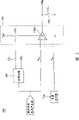
图1为一种传统电源电平检测器100,用于检一芯片所使用的电源VDD的电平,其中,包括一能隙参考电压产生器(Bandgap Voltage Generator)102、一检电压产生电路104、以及一比较器CMP。该能隙参考电压产生器102常见于一般集成电路芯片中,乃用来产生一能隙参考电压VBG供芯片参考。该能隙参考电压VBG为固定值(通常为1.25伏特)不受温度影响、亦不随电源VDD飘移。该检电压产生电路104包括三个晶体管(M1、M2、与M3)以及两个电阻(R1与R2),乃用来在该能隙参考电压VBG产生后,分压该电源VDD,产生一检电压Vdet。如图1所示,该能隙参考电压VBG产生后,晶体管M1导通、晶体管M2操作在饱和区(saturation region)、并且晶体管M3导通且产生一电流流经上述电阻R1与R2。由于晶体管M3的面积远大于晶体管M2,因此晶体管M3操作在线性区(linear region),以电阻型态操作,其电阻值为Ron。电阻Ron、R1、与R2将该电源VDD分压后输出该检电压Vdet。该比较器CMP比较该检电压Vdet以及该能隙参考电压VBG后,输出一标记Flag标示比较结果,以供判断该电源VDD目前的电平。Fig. 1 is a kind of traditional power supply level detector 100, is used for detecting the level of the power supply V DD that a chip uses, wherein, comprises a bandgap reference voltage generator (Bandgap Voltage Generator) 102, a detection voltage generation circuit 104, and a comparator CMP. The bandgap reference voltage generator 102 is commonly used in common integrated circuit chips, and is used to generate a bandgap reference voltage V BG for chip reference. The bandgap reference voltage V BG is a fixed value (usually 1.25 volts) which is not affected by temperature and does not drift with the power supply V DD . The detection voltage generating circuit 104 includes three transistors (M 1 , M 2 , and M 3 ) and two resistors (R 1 and R 2 ), which are used to divide the voltage after the bandgap reference voltage V BG is generated. The power supply V DD generates a detection voltage V det . As shown in FIG. 1 , after the bandgap reference voltage V BG is generated, the transistor M1 is turned on, the transistor M2 operates in the saturation region, and the transistor M3 is turned on and generates a current flowing through the above-mentioned resistor R1 with R2 . Since the area of the transistor M 3 is much larger than that of the transistor M 2 , the transistor M 3 operates in a linear region and operates as a resistor with a resistance value R on . The resistors R on , R 1 , and R 2 divide the power supply V DD to output the detection voltage V det . After the comparator CMP compares the detection voltage V det and the bandgap reference voltage V BG , it outputs a flag indicating the comparison result for judging the current level of the power supply V DD .
然而,该电源VDD遭重置(reset)时,上述传统电源电平检测器100常发生错误。因为该能隙参考电压产生器102在电源VDD被重置后,并不是立即产生该能隙参考电压VBG;必须在该电源VDD回复至一电平以后,才会产生该能隙参考电压VBG举例说明之,假设VDD为5V,该电源VDD被重置后,该能隙参考电压产生器102一开始并不会输出该能隙参考电压VBG,必须等到该电源VDD回升至一电平(例如2.5V)后才会产生该能隙参考电压VBG。如此一来,该电源VDD遭重置后尚未回升至该电平的这一段时间,该比较器CMP的两个输入信号(该能隙参考电压VBG以及该检电压Vdet)都还没有准备好,因此该比较器CMP的运作会发生错误。However, when the power supply V DD is reset, errors often occur in the above-mentioned conventional power level detector 100 . Because the bandgap reference voltage generator 102 does not generate the bandgap reference voltage V BG immediately after the power supply V DD is reset; the bandgap reference voltage must be generated after the power supply V DD returns to a certain level. The voltage V BG is illustrated as an example. Assuming that V DD is 5V, after the power supply V DD is reset, the bandgap reference voltage generator 102 will not output the bandgap reference voltage V BG at the beginning, and must wait until the power supply V DD The bandgap reference voltage V BG will be generated only after returning to a certain level (for example, 2.5V). In this way, during the period when the power supply V DD has not risen to this level after being reset, the two input signals of the comparator CMP (the bandgap reference voltage V BG and the detection voltage V det ) have not yet ready, so the operation of the comparator CMP will fail.
发明内容 Contents of the invention
本发明提供一种新颖的电源电平检测器,可避免上述传统电源电平检测器100在电源重置时所发生的问题。The present invention provides a novel power level detector which can avoid the above-mentioned problems of the conventional power level detector 100 during power reset.
本发明所提出的电源电平检测器包括一电源分压器、一能隙参考电压产生器、一比较电路、一控制电路、以及一强制电路。该电源分压器乃用来分压一电源,以产生一检电压。在重置(reset)该电源后,该能隙参考电压产生器会在该电源回复至一电平后,产生一能隙参考电压。该比较电路乃用来比较该检电压以及该能隙参考电压,以判断该电源的电平。在该能隙参考电压尚未产生时,该控制电路会禁止(disable)该比较电路。在该能隙参考电压产生后,该控制电路由禁止该比较电路切换成使能(enable)该比较电路。该强制电路耦接于该比较电路的输出端,由该控制电路控制。在该比较电路为禁止状态时,该强制电路会强制该比较电路的输出端电压为一定值,以避免该比较电路输出错误信息。The power level detector proposed by the present invention includes a power voltage divider, a bandgap reference voltage generator, a comparison circuit, a control circuit, and a forcing circuit. The power voltage divider is used to divide a power supply to generate a detection voltage. After the power supply is reset, the bandgap reference voltage generator generates a bandgap reference voltage after the power supply returns to a level. The comparison circuit is used to compare the detection voltage and the energy gap reference voltage to judge the level of the power supply. When the bandgap reference voltage has not been generated, the control circuit disables the comparison circuit. After the bandgap reference voltage is generated, the control circuit switches from disabling the comparison circuit to enabling the comparison circuit. The forcing circuit is coupled to the output end of the comparison circuit and controlled by the control circuit. When the comparison circuit is disabled, the forcing circuit will force the voltage at the output terminal of the comparison circuit to be a certain value, so as to prevent the comparison circuit from outputting wrong information.
为让本发明的上述和其它目的、特征、和优点能更明显易懂,下文特举出较佳实施例,并配合附图作详细说明。In order to make the above and other objects, features, and advantages of the present invention more comprehensible, preferred embodiments are listed below and described in detail with accompanying drawings.
附图说明 Description of drawings
图1为一种传统电源电平检测器;Figure 1 is a traditional power level detector;
图2为本发明的电源电平检测器的示意图;Fig. 2 is the schematic diagram of the power level detector of the present invention;
图3为本发明的电源电平检测器的一实施例;Fig. 3 is an embodiment of the power level detector of the present invention;
图4为控制电路304的一实施例;FIG. 4 is an embodiment of the
图5为控制电路304的另一实施例;FIG. 5 is another embodiment of the
图6为该放电电流I与图5的第二晶体管M2的漏源极压差VDS_M2的关系图;FIG. 6 is a relationship diagram between the discharge current I and the drain-source voltage difference V DS_M2 of the second transistor M2 of FIG. 5;
图7为控制电路304的另一实施例;FIG. 7 is another embodiment of the
图8为本发明的电源电平检测器的一实施例;Fig. 8 is an embodiment of the power level detector of the present invention;
图9为本发明的电源电平检测器的一实施例;以及Figure 9 is an embodiment of the power level detector of the present invention; and
图10为本发明的电源电平检测器的一实施例。FIG. 10 is an embodiment of the power level detector of the present invention.
附图符号说明Description of reference symbols
100-传统电源电平检测器;100 - conventional power level detector;
102-能隙参考电压产生器;104-检电压产生电路;102-bandgap reference voltage generator; 104-detection voltage generation circuit;
200-电源电平检测器; 202-电源分压器;200-power level detector; 202-power voltage divider;
204-能隙参考电压产生器;206-比较电路;204-bandgap reference voltage generator; 206-comparison circuit;
208-控制电路; 210-强制电路;208-control circuit; 210-force circuit;
300-电源电平检测器; 302-比较电路;300-power level detector; 302-comparison circuit;
304-控制电路; 402-放电电路;304-control circuit; 402-discharge circuit;
502-放电电路; 702-放电电路;502-discharge circuit; 702-discharge circuit;
802-电源分压器; 902-切换电路;802-power voltage divider; 902-switching circuit;
904-电源分压器; 906-比较电路;904-power voltage divider; 906-comparison circuit;
1002、1004-比较电路; 1006-电源分压器;1002, 1004-comparison circuit; 1006-power voltage divider;
C-电容; CMP-比较器;C-capacitance; CMP-comparator;
CS1-第一控制信号; CS2-第二控制信号;CS 1 - first control signal; CS 2 - second control signal;
Flag、Flag1、Flag2-比较电路的输出标记;Flag, Flag1, Flag2 - output flags of the comparison circuit;
I-放电电流; Inv1-第一反相器;I - discharge current; Inv 1 - first inverter;
Inv2-第二反相器;Inv 2 - the second inverter;
M1、M2、与M3-晶体管; Mn-N型金属氧化物半导体晶体管;M 1 , M 2 , and M 3 -transistors; M n -N-type metal oxide semiconductor transistors;
R1与R2-电阻;R 1 and R 2 - resistance;
SW1-第一开关; SW2-第二开关;SW 1 - first switch; SW 2 - second switch;
SW3-第三开关; SW4-第四开关;SW 3 - third switch; SW 4 - fourth switch;
VBG-能隙参考电压 VDD-电源;V BG - bandgap reference voltage V DD - power supply;
Vdet、Vdet1、Vdet2-检电压。V det , V det1 , V det2 - detection voltages.
具体实施方式 Detailed ways
图2为本发明的电源电平检测器的示意图,其中,一电源电平检测器200包括一电源分压器202、一能隙参考电压产生器204、一比较电路206、一控制电路208、以及一强制电路210。该电源分压器202将一电源VDD分压后,输出一检电压Vdet。该检电压Vdet为该电源VDD的分压。该能隙参考电压产生器204乃用来产生具有固定值的一能隙参考电压VBC。当该电源VDD发生重置(reset)时,该能隙参考电压产生器204必须等待该电源VDD回升至一电平后,才会产生该能隙参考电压VBG。该比较电路206乃用来比较该检电压Vdet以及该能隙参考电压VBG,以判断该电源VDD的电平。该比较电路206的使能/禁止(enable/disable)由该控制电路208控制。在该能隙参考电压VBG尚未产生时,该控制电路208的动作为禁止(disable)该比较电路206。在该能隙参考电压VBG产生后,该控制电路208的动作由禁止该比较电路206切换成使能(enable)该比较电路206。该强制电路210耦接于该比较电路206的输出端,亦由该控制电路208控制。该比较电路206为禁止状态时,该强制电路210会强制该比较电路206的输出端电压为一定值,以避免该比较电路206输出错误的比较结果。2 is a schematic diagram of a power level detector of the present invention, wherein a power level detector 200 includes a power voltage divider 202, a bandgap reference voltage generator 204, a comparison circuit 206, a control circuit 208, and a forcing circuit 210 . The power voltage divider 202 divides a power V DD to output a detection voltage V det . The detection voltage V det is a divided voltage of the power supply V DD . The bandgap reference voltage generator 204 is used to generate a bandgap reference voltage V BC with a fixed value. When the power supply V DD is reset, the bandgap reference voltage generator 204 must wait for the power supply V DD to rise to a certain level before generating the bandgap reference voltage V BG . The comparison circuit 206 is used to compare the detection voltage V det and the bandgap reference voltage V BG to determine the level of the power supply V DD . The enable/disable of the comparison circuit 206 is controlled by the control circuit 208 . When the bandgap reference voltage V BG has not been generated, the action of the control circuit 208 is to disable the comparison circuit 206 . After the bandgap reference voltage V BG is generated, the action of the control circuit 208 is switched from disabling the comparison circuit 206 to enabling the comparison circuit 206 . The forcing circuit 210 is coupled to the output terminal of the comparison circuit 206 and is also controlled by the control circuit 208 . When the comparing circuit 206 is disabled, the forcing circuit 210 will force the voltage at the output terminal of the comparing circuit 206 to be a certain value, so as to prevent the comparing circuit 206 from outputting an erroneous comparison result.
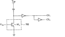
图3为本发明的电源电平检测器的一实施例。电源电平检测器300所采用的比较电路302包括一比较器CMP以及一第一开关SW1。该第一开关SW1耦接于该比较器CMP的电源端与该电源VDD之间,由控制电路304所产生的一第一控制信号CS1控制。该第一开关SW1在该控制电路304禁止该比较电路302时为不导通,并且在该控制电路304使能该比较电路302时为导通。FIG. 3 is an embodiment of the power level detector of the present invention. The
如图3所示,电源电平检测器300以一第二开关SW2实现图2的强制电路210。该第二开关SW2由控制电路304所产生的一第二控制信号CS2控制。由于此实施例将该能隙参考电压VBG输入该比较器CMP的反相输入端,并且将该检电压Vdet输入该比较器CMP的非反相输入端,故该第二开关SW2必须在该比较电路302为禁止状态时将其输出端耦接至一接地端(一定电压端),以确保该比较电路302不会在该比较电路302为禁止状态时误判该检电压Vdet高于该能隙参考电压VBG。As shown in FIG. 3 , the
图4为控制电路304的一实施例,其中包括一电容C、一放电电路402、一第一反相器Inv1、以及一第二反相器Inv2。如图所示,该电容C的第一端点以及第二端点分别耦接该电源VDD以及该放电电路402。该放电电路402在该能隙参考电压VBG产生后启动,用于产生一放电电流I放电该电容C。该第一反相器Inv1的输入端耦接该电容C的第二端点,以输出上述第一控制信号CS1控制上述第一开关SW1。该第一控制信号CS1为高电平时,该第一开关SW1导通,该比较电路302被使能;反之,该第一开关SW1不导通,该比较电路302被禁止。该第二反相器Inv2的输入端耦接该第一反相器Inv1的输出端,用于反相该第一控制信号CS1以产生上述第二控制信号CS2控制该第二开关SW2。该第二控制信号CS2为高电平时,该第二开关SW2导通,反之,则不导通。FIG. 4 is an embodiment of the
在本发明中,上述放电电流I可随着该电容C的第二端点的电压电平下降而减少。图5为控制电路304的另一实施例,所采用的放电电路502为一电流镜,其中,包括一第一晶体管M1以及一第二晶体管M2。该第一晶体管M1的栅极与漏极耦接在一起。该第一与第二晶体管(M1以及M2)的栅极电压皆由该能隙参考电压VBG控制,并且具有同样的栅源极压差。该第二晶体管M2的漏极端耦接该电容C的第二端点。In the present invention, the above-mentioned discharge current I may decrease as the voltage level of the second terminal of the capacitor C decreases. FIG. 5 is another embodiment of the
参阅图5,该电源VDD发生重置但尚未回升至一电平时,该能隙参考电压VBG尚未产生,故该放电电路502尚未开启,该放电电流I为零。此时,该电容C的第二端点的电位会随着其第一端点变化,即随着该电源VDD上升。因此,该电容C的第二端点的电位经该第一与第二反相器Inv1与Inv2处理后,会输出低电平的第一控制信号CS1以及高电平的第二控制信号CS2。参阅图3,藉由上述第一与第二控制信号(CS1以及CS2),该控制电路304禁止该比较电路302并且强制该比较电路302所产生的标记Flag为接地,以避免该比较电路302输出错误的判断结果。Referring to FIG. 5 , when the power supply V DD is reset but has not risen to a certain level, the bandgap reference voltage V BG has not yet been generated, so the discharge circuit 502 has not been turned on, and the discharge current I is zero. At this moment, the potential of the second terminal of the capacitor C changes with the first terminal, that is, rises with the power supply V DD . Therefore, after the potential of the second terminal of the capacitor C is processed by the first and second inverters Inv 1 and Inv 2 , the low-level first control signal CS 1 and the high-level second control signal will be output. CS2 . Referring to FIG. 3, by the above-mentioned first and second control signals (CS 1 and CS 2 ), the
参阅图5,该电源VDD回升至该电平后,该能隙参考电压VBG产生,该放电装置502开启并且产生一放电电流I放电该电容C。图6为该放电电流I与该第二晶体管M2的漏源极压差VDS_M2的关系图。如图6所示,该放电电流I刚产生时,该电容C的第二端点的电位(即该第二晶体管M2的漏源极压差VDS_M2)为V0,该放电电流I=I0。该电容C的第二端点的电位(VDS_M2)在放电过程中逐渐下降,如图6所示,该放电电流I亦随之逐渐降低,最后两者皆降至零。上述放电程序会令该电容C的第二端点电位经该第一与第二反相器Inv1与Inv2处理后,输出高电平的第一控制信号CS1、及低电平的第二控制信号CS2。因此,该比较电路302被使能,并且该比较电路302的输出端不再被强制接地。该比较电路302得以开始正常运作。Referring to FIG. 5 , after the power supply V DD rises back to the level, the bandgap reference voltage V BG is generated, the discharge device 502 is turned on and generates a discharge current I to discharge the capacitor C. FIG. 6 is a graph showing the relationship between the discharge current I and the drain-source voltage difference V DS_M2 of the second transistor M 2 . As shown in FIG. 6, when the discharge current I is just generated, the potential of the second terminal of the capacitor C (that is, the drain-source voltage difference V DS_M2 of the second transistor M2 ) is V 0 , and the discharge current I=I 0 . The potential (V DS_M2 ) of the second terminal of the capacitor C gradually decreases during the discharge process, as shown in FIG. 6 , the discharge current I also decreases gradually, and finally both of them drop to zero. The above discharge procedure will make the potential of the second terminal of the capacitor C be processed by the first and second inverters Inv 1 and Inv 2 to output a high-level first control signal CS 1 and a low-level second
图7为控制电路304的另一实施例,所采用的放电电路702为一N型金属氧化物半导体晶体管Mn,其栅极耦接该能隙参考电压VBG、其漏极耦接该电容C的第二端点、并且其源极接地。由上述实施例可知,本发明的放电电路在该电容C的第二端点的电位降至零后即停止提供该放电电流I,故本发明不需要耗费大量能量。FIG. 7 is another embodiment of the
图8为本发明的另一实施例,其中,所采用的电源分压器802乃由串联在该电源VDD与一接地端之间的多个电阻(本实施例为R1与R2)所组成。本发明采用单纯电阻分压,使用者可轻易掌握该检电压Vdet与该电源VDD的关系。反观图1的传统电源电平检测器100,该检电压产生电路104的晶体管M3的电阻值Ron会随着工艺过程变化,不易掌握,容易造成使用者困扰。FIG. 8 is another embodiment of the present invention, wherein the adopted power
图9为本发明的另一实施例,其中,还包括一切换装置902,耦接于该电源分压器904与该比较电路906之间,用于在该比较电路906为禁止状态时,将该检电压Vdet切换成一接地端以输入该比较电路906。如图所示,该切换装置902包括一第三开关SW3、以及一第四开关SW4。该第三开关SW3在该比较电路906被使能(该第一控制信号CS1为高电平)时导通,用于耦接该检电压Vdet至该比较电路906。该第四开关SW4在该比较电路906被禁止(该第二控制信号CS2为高电平)时导通,用于耦接该接地端至该比较电路906。FIG. 9 is another embodiment of the present invention, which further includes a
图10为本发明的另一种实施例,其中包括多组比较电路(1002与1004)。本实施例的电源分压器1006会输出两组检电压(Vdet1与Vdet2),分别输入比较电路1002与1004。所述比较电路1002与1004的使能与否、以及其输出端所耦接的强制电路的动作与否皆和本发明其它实施例相同。藉由本实施例,使用者可由标记Flag1与Flag2判断该电源VDD目前位于某一电压范围内。FIG. 10 is another embodiment of the present invention, which includes multiple comparison circuits (1002 and 1004). The
本发明虽以较佳实施例揭露如上,然其并非用于限定本发明的范围,任何熟习此项技艺者,在不脱离本发明的精神和范围内,当可做些许的更动与润饰,因此本发明的保护范围当视本发明的申请专利范围所界定者为准。Although the present invention is disclosed as above with preferred embodiments, it is not intended to limit the scope of the present invention. Anyone skilled in this art can make some changes and modifications without departing from the spirit and scope of the present invention. Therefore, the scope of protection of the present invention should be defined by the patent scope of the present invention.
Claims (10)
Applications Claiming Priority (2)
| Application Number | Priority Date | Filing Date | Title |
|---|---|---|---|
| US82429006P | 2006-09-01 | 2006-09-01 | |
| US60/824,290 | 2006-09-01 |
Publications (2)
| Publication Number | Publication Date |
|---|---|
| CN1996025A CN1996025A (en) | 2007-07-11 |
| CN100451663C true CN100451663C (en) | 2009-01-14 |
Family
ID=38251168
Family Applications (1)
| Application Number | Title | Priority Date | Filing Date |
|---|---|---|---|
| CNB2007100016616A Active CN100451663C (en) | 2006-09-01 | 2007-01-09 | Power supply level detector |
Country Status (2)
| Country | Link |
|---|---|
| CN (1) | CN100451663C (en) |
| TW (1) | TWI312869B (en) |
Families Citing this family (14)
| Publication number | Priority date | Publication date | Assignee | Title |
|---|---|---|---|---|
| CN101923145B (en) * | 2009-06-15 | 2013-01-23 | 凌通科技股份有限公司 | Power detection circuit, portable device and method for preventing data loss |
| CN101726649B (en) * | 2009-10-30 | 2013-04-24 | 海洋王照明科技股份有限公司 | Signal detection circuit, emergency power switching device and emergency light |
| CN103516349A (en) * | 2012-06-26 | 2014-01-15 | 深圳市威尔科思技术有限公司 | High-voltage compatible input system |
| US9081396B2 (en) * | 2013-03-14 | 2015-07-14 | Qualcomm Incorporated | Low power and dynamic voltage divider and monitoring circuit |
| WO2018009240A2 (en) * | 2015-11-12 | 2018-01-11 | University Of Rochester | Superconducting system architecture for high-performance energy-efficient cryogenic computing |
| CN105403791A (en) * | 2015-12-09 | 2016-03-16 | 华南理工大学 | Device starting detection circuit |
| TWI629492B (en) * | 2017-08-03 | 2018-07-11 | 新唐科技股份有限公司 | System and method for testing reference voltage circuit |
| CN111092613B (en) * | 2018-10-23 | 2023-12-05 | 雅特力科技(重庆)有限公司 | Power-on reset circuit and related reset method |
| CN111987754A (en) * | 2019-05-24 | 2020-11-24 | 凹凸电子(武汉)有限公司 | Movable equipment and control method for supplying power to loads |
| CN112787486B (en) * | 2019-11-08 | 2023-04-28 | 奇景光电股份有限公司 | Power ready signal generating device and operation method thereof |
| US11888474B2 (en) | 2020-06-03 | 2024-01-30 | Changxin Memory Technologies, Inc. | On die termination circuit and memory device |
| CN113760802B (en) * | 2020-06-03 | 2024-05-14 | 长鑫存储技术有限公司 | On-chip termination circuit and memory device |
| CN116482564A (en) * | 2023-04-26 | 2023-07-25 | 星宸科技股份有限公司 | Power detection device and power detection method |
| CN118837605B (en) * | 2024-06-25 | 2025-10-31 | 珠海全志科技股份有限公司 | Automatic power supply voltage detection device and method and electronic equipment |
Citations (5)
| Publication number | Priority date | Publication date | Assignee | Title |
|---|---|---|---|---|
| CN2432731Y (en) * | 2000-05-30 | 2001-05-30 | 麦肯积体电路股份有限公司 | Power supply voltage detection circuit |
| CN2438273Y (en) * | 2000-06-12 | 2001-07-04 | 麦肯积体电路股份有限公司 | Circuit for detecting power supply voltage cut-in point |
| CN1381732A (en) * | 2002-04-15 | 2002-11-27 | 威盛电子股份有限公司 | voltage potential detector |
| CN1494759A (en) * | 2001-11-30 | 2004-05-05 | 索尼公司 | Power generation circuit, display device and portable terminal device |
| US20040113681A1 (en) * | 2002-10-12 | 2004-06-17 | Oki Electric Industry Co., Ltd. | Voltage sensing circuit |
-
2006
- 2006-12-29 TW TW95149874A patent/TWI312869B/en active
-
2007
- 2007-01-09 CN CNB2007100016616A patent/CN100451663C/en active Active
Patent Citations (5)
| Publication number | Priority date | Publication date | Assignee | Title |
|---|---|---|---|---|
| CN2432731Y (en) * | 2000-05-30 | 2001-05-30 | 麦肯积体电路股份有限公司 | Power supply voltage detection circuit |
| CN2438273Y (en) * | 2000-06-12 | 2001-07-04 | 麦肯积体电路股份有限公司 | Circuit for detecting power supply voltage cut-in point |
| CN1494759A (en) * | 2001-11-30 | 2004-05-05 | 索尼公司 | Power generation circuit, display device and portable terminal device |
| CN1381732A (en) * | 2002-04-15 | 2002-11-27 | 威盛电子股份有限公司 | voltage potential detector |
| US20040113681A1 (en) * | 2002-10-12 | 2004-06-17 | Oki Electric Industry Co., Ltd. | Voltage sensing circuit |
Non-Patent Citations (1)
| Title |
|---|
| 高精度宽容限电源电压检测电路的设计. 张颖,潘亮.中国集成电路,第68期. 2005 * |
Also Published As
| Publication number | Publication date |
|---|---|
| TW200813443A (en) | 2008-03-16 |
| CN1996025A (en) | 2007-07-11 |
| TWI312869B (en) | 2009-08-01 |
Similar Documents
| Publication | Publication Date | Title |
|---|---|---|
| CN100451663C (en) | Power supply level detector | |
| US5440254A (en) | Accurate low voltage detect circuit | |
| CN102025263A (en) | Power supply starting detection circuit | |
| KR101646910B1 (en) | Semiconductor device including power on reset circuit | |
| EP3550723B1 (en) | Pad tracking circuit for high-voltage input-tolerant output buffer | |
| CN108667443A (en) | A kind of electrification reset circuit | |
| CN111693759B (en) | Voltage detector | |
| JP2004163315A (en) | Voltage detecting circuit | |
| CN109964276B (en) | Circuitry for Bleeding Supply Voltage from Devices in Power-Down State | |
| CN109696940B (en) | Method for identifying faults at the output of a device and system thereof | |
| CN106921371B (en) | Low-power-consumption power-on reset circuit | |
| CN115754440B (en) | Voltage detection circuit with low power consumption and simple structure | |
| US9086434B1 (en) | Methods and systems for voltage reference power detection | |
| US8344779B2 (en) | Comparator circuit with hysteresis, test circuit, and method for testing | |
| CN111007910B (en) | Open-drain output control circuit | |
| JP2001339285A (en) | Power off detection circuit | |
| CN106972852B (en) | Interface circuit and electronic equipment | |
| KR20210127207A (en) | blackout detection circuit | |
| CN119543898B (en) | Power-on reset circuit with hysteresis effect | |
| CN115201542B (en) | Voltage detection circuit | |
| US20250202459A1 (en) | Control method of power switch module and associated circuit | |
| US7463074B2 (en) | Integrated circuit and method for generating a ready signal | |
| KR200222131Y1 (en) | Power fail detecting circuit | |
| US8194491B2 (en) | Power-up circuit | |
| KR100223672B1 (en) | Semiconductor memory device holding in check active peak current |
Legal Events
| Date | Code | Title | Description |
|---|---|---|---|
| C06 | Publication | ||
| PB01 | Publication | ||
| C10 | Entry into substantive examination | ||
| SE01 | Entry into force of request for substantive examination | ||
| C14 | Grant of patent or utility model | ||
| GR01 | Patent grant |