Summary of the invention
Execution mode of giving an example of the present invention comprises the method that is used to form multicore platelet chip level Chip Packaging, need be in order not form globally interconnected and to carry out complanation with the integrated of the chip of different disposal step and different materials manufacturing to engaging chip surface for facility.
A kind of execution mode of giving an example relates to a kind of method that forms the encapsulation of multicore platelet chip level.This method comprises: form a plurality of dissimilar chips on a plurality of chip substrate, wherein, each in described a plurality of chip substrate is used for only forming the chip of single type; Described a plurality of dissimilar chips are separated from described a plurality of chip substrate; Form depression in carrier substrates, wherein, each depression holds in described a plurality of dissimilar chip; Described a plurality of chips are installed in their corresponding depressions in described carrier substrates, make the end face coplane basically of the end face of described a plurality of chips and described carrier substrates.Described dissimilar chip can be memory chip, logic chip, MEMS device, RF circuit or passive device.
The described step that forms a plurality of chips on a plurality of chip substrate can also comprise: join wafer to STI in the described chip substrate each (shallow trench isolation from) zone, make adjacent with described STI district, between described wafer and chip substrate, form the space, wherein, zone in the wafer above the STI district forms the chip chamber zone, and the zone in the wafer above the space forms chip region.In addition, can form discrete device in the chip chamber zone of chip substrate, wherein, described discrete device can be inductor, decoupling capacitor or Electrostatic Discharge diode.
In said method, before joining wafer to the STI district, this method can also comprise: with the dielectric layer patterning on the chip substrate; The described pattern dielectric layer of etching is to form sheet outskirt (off-chip area); In described outskirt, form the STI district; Remove the dielectric layer between the described outskirt.
Described method can also comprise: the described wafer of attenuate; In described thinned wafer, form device; On described thinned wafer, form BEOL (back end of line, Back-End-Of-Line) interconnection; In described chip region, form last device (finishing device) and interconnection, to finish the formation of described a plurality of chips.
Described a plurality of chips separation steps on described a plurality of chip substrate can also be comprised: with the end face of the described thinned wafer of passivation layer plating; Cutting or etched trench, the chip region of passing described thinned wafer arrives described space, thereby described a plurality of chips are separated from described a plurality of chip substrate.
The step that forms depression in described carrier substrates can also comprise: join wafer in the carrier substrates STI district, feasible and STI district is adjacent to form the space between wafer and carrier substrates, wherein, the zone above the STI district in the wafer forms the chip chamber zone, and the zone above the space in the wafer forms chip region.
The step that described a plurality of chips are installed in its corresponding depression can also comprise: identical with the described space basically dielectric layer of deposition thickness in described chip region; Described a plurality of chips are aimed in its corresponding depression.
The execution mode that another kind is given an example relates to a kind of method that forms the encapsulation of multicore platelet chip level.This method comprises: form a plurality of identical or dissimilar chips on the relevant chip substrate; Described a plurality of chips are separated from corresponding chip substrate; On carrier substrates, form a plurality of depressions, make in described a plurality of depression each hold the chip of predefined type; From described a plurality of identical or dissimilar chips, select each the pairing chip of chip of predefined type in described a plurality of depressions; And selected chip is installed in its corresponding depression, make the end face coplane basically of the end face of selected chip and carrier substrates.
Preferably, provide a kind of method that forms the encapsulation of multicore platelet chip level, comprised the following steps: in carrier substrates, to form shallow trench isolation from (STI) zone; Join wafer in the carrier substrates STI district, make and between wafer and carrier substrates, be adjacent to form the space with the STI district, wherein, the zone in the described wafer above described STI district forms the chip chamber zone, and the zone in the described wafer above described space forms chip region; The described wafer of attenuate; On the wafer of attenuate, form the BEOL interconnection; End face with the described thinned wafer of passivation layer plating; In the chip region of described thinned wafer, cut groove, make that the predetermined portions of described thinned wafer is separated, thereby in described thinned wafer, form depression.
From below in conjunction with the detailed description of accompanying drawing, can know above-mentioned and execution mode, feature, aspect and advantage that other is given an example of the present invention more to the execution mode of giving an example.
Embodiment
Execution mode of giving an example of the present invention as described herein provides the cost effective method of making the encapsulation of multicore platelet chip level, and wherein, chip and carrier all use " local wafer joint " and " local wafer cutting " technology to form.According to execution mode of giving an example of the present invention, general, the use of local wafer joining technique allows forming chip in the not engaging zones at thin silicone layer on the chip carrier, is forming depression in the not engaging zones at the top thin silicon layer on the carrier substrates.In the chip integrated technique, use the partial cut technology that chip is cut down from chip carrier, use same local wafer microtomy on carrier substrates, to form depression.At last, be placed and join in its corresponding depression from chip same or the different chips carrier.
Figure 1A-1E illustrates according to a kind of execution mode of giving an example of the present invention, is used to form the method for multicore wafer encapsulation.More specifically, Figure 1A-1E illustrates the execution mode of giving an example according to of the present invention, forms depression in carrier substrates 2 (" cs "), places the technology of chip in the depression in carrier substrates.
See Figure 1A, be used on the surface of carrier substrates 2, forming the silicon layer 6 of depression in the oxide position of carrier substrates 28 local engagement.In addition, unoxidized regional 3, silicon layer 6 does not join on the carrier substrates 2, thereby under silicon layer 6, is forming microscopic voids 16 (shown in the part enlarged drawing among Figure 1A) in the oxide regions 3.In addition, space 16 comprises air or nitride layer.In addition, can deposit CVD nitride film and to patterning, make space 16 comprise nitride film.In brief, microscopic voids, CVD nitride film or rough surface have stoped the lip-deep joint of carrier substrates.
See the guide wire of alternative shape of Figure 1A, this zoomed-in view illustrates carrier substrates 2, comprise shallow trench isolation from (STI) zone 8, silicon layer 6, be formed between silicon layer 6 and the carrier substrates 2 and the part in the space 16 adjacent with STI district 8.Preferably, space 16 comprises air, nitride layer or coarse silicon face, engages to stop.
Next, in Figure 1B, on silicon layer 6, carry out traditional metallization (metallization) technology, thereby form interconnection layer 10.Then, in carrier substrates 2, form the depression 12,13,14 and 15 of Fig. 1 C.Use the local wafer microtomy in carrier substrates 2, to form depression.
Fig. 1 D and Fig. 1 E illustrate chip 11A, 24,26 and 28 from a plurality of false carriers are transferred to their corresponding depression 12-15 carrier substrates 2.Should be appreciated that chip 11A, 24, the dissimilar chip of 26 and 28 representatives, wherein, the chip of each type is formed on the independent carrier substrates.In addition, can be on carrier substrates 2 deposition insulating layer 20, being held in place from a plurality of chips of different false carriers, to fill the space that may be present between chip and the STI district 8, and provide the end face of complanation, thereby can on carrier substrates 2, form globally interconnected 22, shown in Fig. 1 E.
Fig. 2 A-2C illustrates execution mode that another kind according to the present invention gives an example forms chip on false carrier method.See Fig. 2 A, locate in STI district 8 ' and will be used to form the semiconductor layer 6 ' local engagement of chip to false carrier 4.Semiconductor layer 6 ' can be the compound of silicon, germanium, GaAs, CdSe, II family element and IV family element or the compound of III family element and V group element.In other words, can form different chips with different materials.After chip 11A-11E is cut down from false carrier 4, at least one chip, for example chip 11A can be assembled in its corresponding depression (for example depression 14) in carrier substrates 2.Here, only illustrate a false carrier 4 or s1, still, be to be understood that, many other false carriers can be arranged, and they have identical or different semiconductor layers to make many dissimilar chips, for example memory chip, logical circuit, MEMS device, RF circuit or passive device.In addition, shown in Fig. 2 B, each false carrier can be made a plurality of identical chip 11A-11E.Have rectangular shape although should be appreciated that the device 11A-11E shown in Fig. 2 B, chip 11A-11E can form has many different shapes, for example square, polygon, u shape, v shape etc.In addition, chip 11A-11E can be formed and have different identical shaped of size.For example, chip 11A-11E can be the capacitor of the rectangular shape that is uneven in length.
In addition, semiconductor layer 6 ' does not join on the false carrier 4 in oxide regions 3 ' not, thereby forms space 16 ' in oxide regions 3 ' not, shown in the enlarged drawing among Fig. 2 A.In addition, space 16 ' can comprise air or nitride layer.The use that should be noted that the local wafer joining technique has realized the stricter control to the thickness that is illustrated in silicon layer 6 among Figure 1A and the 2A and semiconductor layer 6 ' respectively.In the enlarged drawing of the part of Fig. 2 A, false carrier 4 comprise shallow trench isolation STI district 8 ', semiconductor layer 6 ' and be formed on semiconductor layer 6 ' and false carrier 4 between, with STI district 8 ' adjacent areas 16 '.Preferably, this zone 16 ' comprises air, nitride layer or coarse silicon face, engages to stop.
Next, form device (not shown) in the semiconductor layer 6 ' on false carrier 4.Go up at the semiconductor layer 6 ' of Fig. 2 B then and carry out traditional metallization process, thereby form the interconnection layer 10 ' that has approximately identical thickness with the interconnection layer 10 shown in Figure 1B.Then, the chip 11A-11E of separation graph 2C from the false carrier 4.Use local wafer microtomy separating chips 11A-11E from the false carrier 4.At least one is from the chip 11A-11E of false carrier 4, and chip 11A for example is placed to corresponding depression in the carrier substrates 2 that is formed on Fig. 1 C for example in the depression 14.Each false carrier can have identical or different semiconductor top layers 6 '.But, in false carrier, make identical chip.For example, the first false carrier s1 with silicon top layer can be used for making a plurality of DRAM memory chips.The second false carrier s2 with magnetic top layer can be used for making a plurality of MRAM chips.At assembly process, can be placed in its corresponding depression in carrier substrates cs from each at least one chip among the false carrier s1-sn.For example, in the process of assembling multicore platelet chip level encapsulation, can be placed in their corresponding depressions in carrier substrates cs from the MRAM chip of the second false carrier s2 with from four dram chips of the first false carrier s1.
It is very important that carrier substrates cs with depression is used identical technology (comprising deposition of materials and THICKNESS CONTROL) with the false carrier of making chip in the above, so that pocket depth and chip thickness can mate.In other words, all chips of finishing should have the substantially the same thickness suitable with the degree of depth of depression.By using mask and etching technique to carry out the local wafer cutting, accurately to be controlled at size and the aligning between the chip in each self-corresponding depression.Then each chip is placed in its corresponding depression, and it is adhered in the depression with suitable bonding or use thermal grease (thermal paste).This technology because all chips all face up, thereby can be carried out globally interconnected formation without any need for extra complanation or carrier transfer step, so that the chip electrical interconnection on the carrier substrates is got up.
In addition, the local wafer microtomy can be with chip from the cutting of false carrier and take off and do not damage false carrier.By on wafer, carrying out partial cut, preferably just cut the top semiconductor layer on the false carrier, thereby chip is taken off from false carrier.Because this zone does not join on the false carrier, in case carry out partial cut in wafer, chip just separates from false carrier.In other words, only when the wafer local engagement is to false carrier, just can carry out the local wafer microtomy.The advantage of local engagement and partial cut is, in case chip is separated from its false carrier separately, chip thickness just basically with the pocket depth coupling of carrier substrates, thereby the necessity of having exempted coarse polishing step.
Fig. 3 A-3L illustrates according to a kind of execution mode of giving an example of the present invention, is formed for the chip of multicore platelet chip level encapsulation and the method for carrier.In Fig. 3 A, deposit dielectric layer 301 on the end face of false carrier 30 as one kind 0.The thickness of dielectric layer 301 has been determined the degree of depth in the space that will form in step subsequently.In Fig. 3 B, use traditional photoetching technique with dielectric layer 301 patternings with photoresist mask 303.In Fig. 3 C, use dry method etch technology etch dielectric layer 301 to form sheet outskirt (off-chip area) 304.Sheet outskirt 304 will be used as the junction in step subsequently.In Fig. 3 D, in sheet outskirt 304, form shallow trench isolation from (STI) district 305.In Fig. 3 E, remove dielectric layer 301 to form interstitial area 306.In Fig. 3 F, in STI district 305 wafer 307 is joined on the false carrier 30 as one kind 0, thereby in interstitial area 306, form space 302.Zone in the wafer 307 above space 302 forms chip region 312, and the zone in the wafer 307 above STI district 305 forms chip chamber zone 311.In Fig. 3 G,, thereby form thinned wafer 308 with wafer 307 attenuates.Preferably, the thickness of thinned wafer 308 is about 50 to about 100 microns.This thinning technique and THICKNESS CONTROL have been developed fully, therefore are not further elaborated at this.In Fig. 3 H, at the thinned wafer layer 308 inner device 310 that forms.In Fig. 3 I, on the wafer layer 308 of attenuate, form BEOL back end of line interconnection in other words 309.In addition, in the chip chamber zone 311 of the thinned wafer layer 308 of false carrier 30 as one kind 0, form discrete device.Discrete device can comprise inductor, decoupling capacitor, Electrostatic Discharge diode or other any discrete device.Just, before cutting out chip 315A and 315B, these discrete devices are arranged in the chip chamber zone, can be used for testing and monitoring the work that is formed on chip wherein.In addition, after forming BEOL interconnection 309, with the device and interconnection (not shown) filled core section 312A and the 312B that finish, to finish the formation of chip 315A and 315B, shown in Fig. 3 J.
See Fig. 3 J, plating passivation layer 314 on the end face of thinned wafer layer 308, the wafer that is used to cut with preparation.Because thinned wafer layer 308 is thinner, can use laser cutting technique or reactive ion etching to come to downcut and separating chips 315A and 315B from thinned wafer layer 308 by cutting groove 319 around chip 315A and 315B shown in Fig. 4 A.Preferably, groove width is about 15 microns to about 40 microns.Fig. 3 K illustrates to be used to cut to pass thinned wafer layer 308 and arrives spaces 302, thus the ideal position 320 that chip 315A and 315B are separated from thinned wafer layer 308.In addition, the device that forms in the chip chamber of false carrier or chip carrier zone is only being used for testing and monitoring the chip that forms therein, because in case chip takes off from false carrier, then false carrier is just of no use and go out of use.
In addition, above-mentioned technology also is used for forming depression in carrier substrates.-in addition, to not carrying out in the carrier substrates and in LED reverse mounting type, forming the relevant step of chip.But, can in the chip chamber zone of carrier substrates, form discrete device.Discrete device can comprise inductor, decoupling capacitor, Electrostatic Discharge diode or other any discrete device.Just, when cutting out depression, these discrete devices are in the chip chamber zone, thereby these discrete devices can form the part of system afterwards as chip.
Fig. 3 L illustrates the structure according to the carrier substrates of a kind of execution mode of giving an example of the present invention.More specifically, Fig. 3 L illustrates with the carrier substrates structure not engaging zones take off after of false chip from carrier substrates.Present 3L with the aid of pictures is cutting from carrier substrates 300 ' and is separating false chip (not shown) afterwards, forms structure 330, useful device 316A, 316B and the 316C that comprise depression 317A and 317B and make in chip chamber zone 311.
Shall also be noted that can the different time also/or form depression and chip from different sources at different wafer because treatment step is identical, the thickness of chip and the degree of depth of depression are followed (tracked) closely.Before chip being put into its corresponding depression, must fill space 302 by the deposit dielectric layer identical with the thickness of the dielectric layer 301 of Fig. 3 A.Preferably, before the depression of chip being put into separately, fill space 302 with dielectric layer, adhesive phase or thermal grease (thermal paste).As a result, when all chips are put into each self-corresponding depression, the end face of all chips basically with the end face coplane of wafer with depression, form the required step of the integrated encapsulation of multicore platelet chip level and the quantity of technology thereby reduce.In addition, be formed on the work that discrete device in the chip chamber zone of false carrier is used to test and monitor formation chip thereon.Thereby the discrete device that is formed in the chip chamber zone of carrier substrates is the inalienable part of multicore platelet chip level encapsulation.
Fig. 4 A is the end view that is illustrated in the chip of Fig. 3 K after carrying out local wafer slice technology.See Fig. 4 A, thereby, removed the predetermined portions of thinned wafer layer 308 by using the local wafer microtomy that chip 315A is separated from carrier substrates 300.In addition, define buffering area 318 around chip 315A.Here it shall yet further be noted that and carried out a kind of cutting technique, arrive space 302 by cutting thinned wafer layer 308, thereby chip 315A is got off from substrate separation.In other words, 302 places are not attached on the substrate in the space owing to chip 315A, in case the wafer layer 308 of attenuate is cut and be cut into piece around chip 315A, chip 315A just separates.
Fig. 4 B is the vertical view of the chip shown in Fig. 3 K after carrying out local wafer slice technology.See Fig. 4 B, illustrated chip 315A has periphery along 315A, the buffering area 318 adjacent with cutting groove 319.
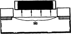
Fig. 5 A-5C illustrates a kind of execution mode of giving an example according to the present invention and separates the method that is formed on the chip on the carrier substrates.In Fig. 5 A, the LED reverse mounting type layer 510 with thickness d 1 is engaged on the thicker substrate 530 that thickness is d2, to keep mechanical strength during handling and processing.Preferably, thickness d 1 is about 50 microns to about 300 microns.Engaging zones 521 is formed by the wafer layer 510 on the oxide skin(coating) 540 that joins patterning to.Engaging zones 522 is not from the disappearance of oxide skin(coating).In LED reverse mounting type layer 510, do not forming chip 520 circuit wafer (die) in other words in the engaging zones.But, should be noted that wafer layer 510 can be the compound of silicon, germanium, GaAs, CdSe, II family element and VI family element or the compound of III family element and IV family element.Carry out local wafer slice technology: photoresist mask 500 is formed on the top at LED reverse mounting type layer 510, by photoetching photoresist mask 500 is exposed.After forming photomask 500, carry out dry method or wet etching process, etching LED reverse mounting type layer 510.Perhaps, also can use the direct laser cutting of maskless to carry out part section, separating chips 520.Fig. 5 B illustrates etching and passes the groove 550 that LED reverse mounting type layer 510 arrives the formation around the not engaging zones 522 of chip 520.In Fig. 5 C, never chip 520 or circuit wafer are removed in bonding land 522, thereby form depression 560.Can use high-density plasma or reactive ion etching to come effectively etched trench 550 or diced chip circuit wafer in other words.Similarly, can form depression by remove false chip from substrate.The degree of depth of depression should have and the actual substantially the same thickness of chip, so that after chip was installed, the end face of chip and the end face of wafer be coplane basically.By carrying out this method, encapsulation is just all set carried out global chip to chip wiring, and without any need for further preparation, such as the end face of the chip of complanation joint.
Execution mode of giving an example of the present invention comprises the method that is used to form the encapsulation of multicore platelet chip level that will use the chip of different processing steps and made to integrate in the mode of economy that is beneficial to.The flowchart illustrations of Fig. 6 according to execution mode of giving an example of the present invention, be used to form the method for multicore platelet chip level encapsulation.See Fig. 6 now, on chip substrate, form a plurality of chips (step 602).Next, by false chip is separated from carrier substrates, in carrier substrates, form depression (step 604).Then, from chip substrate separating chips (step 606).Should be appreciated that step 604 can be carried out simultaneously with 606 or carry out according to different orders.To be installed to from the chip that chip substrate separates then in the predetermined depression the carrier substrates, make the end face coplane (step 608) basically of the end face of chip and carrier substrates.
The flowchart illustrations of Fig. 7 according to a kind of execution mode of giving an example of the present invention, on chip substrate, form the method for a plurality of chips.Particularly, Fig. 7 illustrates a kind of method of giving an example of the step 602 of Fig. 6, and it relates to and form chip on chip substrate.See Fig. 7 now, the dielectric layer on the chip substrate is carried out patterning (step 702).Next, the etched pattern dielectric layer forms sheet outskirt (step 704).In the sheet outskirt, form shallow trench isolation from (STI) district (step 706).Then, the dielectric layer (step 708) between the removal sheet outskirt.Next, join wafer to the STI district, feasible and STI district is adjacent to form the space between wafer and chip substrate, and wherein, the zone in the wafer above the STI district forms the chip chamber zone, and the zone of top, space forms chip region (step 710).Then, thinned wafer (step 712).In the wafer of attenuate, form device (step 714) then.Next, formed therein and formed BEOL interconnection (step 716) on the thinned wafer of device.At last, in the chip region of thinned wafer, form last device and interconnection, to finish the formation (step 718) of chip.In addition, should be appreciated that above-mentioned technology can be used for forming many dissimilar chips on different chip substrate.
The flowchart illustrations of Fig. 8 according to a kind of execution mode of giving an example of the present invention, be used for forming the method for a plurality of depressions in carrier substrates.Particularly, Fig. 8 illustrates the method for giving an example of the step 604 among Fig. 6, and it relates to and form depression in carrier substrates.See Fig. 8 now, to the dielectric layer patterning (step 802) on the carrier substrates.Next, the etched pattern dielectric layer is to form sheet outskirt (step 804).Then, in the sheet outskirt, form shallow trench isolation from (STI) district (step 806).Remove the dielectric layer (step 808) between the sheet outskirt then.Next, join wafer to the STI district, feasible and STI district is adjacent to be formed on the space between wafer and the carrier substrates, and wherein, the zone in the wafer above the STI district forms the chip chamber zone, and the zone of top, space forms chip region (step 810).Then, thinned wafer (step 812).Next, on thinned wafer, form BEOL interconnection (step 814).End face (step 816) with the described thinned wafer of passivation layer plating.Next, in the chip region of wafer, cut groove, make that the predetermined portions of wafer or false chip are separated, thereby in wafer, form depression (step 818).
The flowchart illustrations of Fig. 9 according to a kind of execution mode of giving an example of the present invention, the method that chip is separated from chip substrate.Particularly, Fig. 9 illustrates the method for giving an example of the step 606 among Fig. 6, and it relates to chip is separated from chip substrate.See Fig. 9 now, with the end face of the described thinned wafer of passivation layer plating, with protection chip (step 902).Next, the cutting groove, the chip region of passing wafer arrives the space, thereby chip is separated (step 904) from chip substrate.
The flowchart illustrations of Figure 10 according to a kind of execution mode of giving an example of the present invention, will be installed to the method in the predetermined depression the carrier substrates from the chip that chip substrate separates.Particularly, Figure 10 illustrates a kind of method of giving an example of step 608 among Fig. 6.See Figure 10 now, have the adhesive phase or the thermal grease (step 1002) of identical thickness in deposit of the bottom of depression and described space.Next, chip is placed in its corresponding depression and aligning (step 1004).In addition, replace described adhesive phase or thermal grease, can use the dielectric layer that has same scale with described space.
In a word, execution mode of giving an example of the present invention provides the effective ways that form the encapsulation of coplane multicore platelet chip level, wherein, uses local wafer joint and local wafer slice technology to come to form chip and depression in wafer surface.The chip of finishing is installed in the depression of correspondence of wafer, on the top flat surface of joint chip, forms the globally interconnected of chip chamber.These method facilities integrated with the chip of different processing steps and made.No longer need to use coarse flatening process to make the top surface planeization of chip such as chemico-mechanical polishing.Because chip is accurately aimed at mutually and all chips are all installed up, module has all set been carried out global routing (global wiring), and this does not just need chip is turned from upside down position.
Concrete diagram and description have been carried out at execution mode of giving an example of the present invention above.One of ordinary skill in the art will appreciate that form of the present invention and details can be carried out various variations and the scope of the present invention that do not break away from claims and limited.