CN100435373C - Semiconductor memory device and manufacturing method thereof - Google Patents
Semiconductor memory device and manufacturing method thereof Download PDFInfo
- Publication number
- CN100435373C CN100435373C CNB2004100343559A CN200410034355A CN100435373C CN 100435373 C CN100435373 C CN 100435373C CN B2004100343559 A CNB2004100343559 A CN B2004100343559A CN 200410034355 A CN200410034355 A CN 200410034355A CN 100435373 C CN100435373 C CN 100435373C
- Authority
- CN
- China
- Prior art keywords
- layer
- interlayer insulating
- forming
- insulating layer
- heating
- Prior art date
- Legal status (The legal status is an assumption and is not a legal conclusion. Google has not performed a legal analysis and makes no representation as to the accuracy of the status listed.)
- Expired - Fee Related
Links
Images


Classifications
-
- H—ELECTRICITY
- H10—SEMICONDUCTOR DEVICES; ELECTRIC SOLID-STATE DEVICES NOT OTHERWISE PROVIDED FOR
- H10D—INORGANIC ELECTRIC SEMICONDUCTOR DEVICES
- H10D84/00—Integrated devices formed in or on semiconductor substrates that comprise only semiconducting layers, e.g. on Si wafers or on GaAs-on-Si wafers
-
- H—ELECTRICITY
- H10—SEMICONDUCTOR DEVICES; ELECTRIC SOLID-STATE DEVICES NOT OTHERWISE PROVIDED FOR
- H10B—ELECTRONIC MEMORY DEVICES
- H10B63/00—Resistance change memory devices, e.g. resistive RAM [ReRAM] devices
- H10B63/30—Resistance change memory devices, e.g. resistive RAM [ReRAM] devices comprising selection components having three or more electrodes, e.g. transistors
-
- H—ELECTRICITY
- H10—SEMICONDUCTOR DEVICES; ELECTRIC SOLID-STATE DEVICES NOT OTHERWISE PROVIDED FOR
- H10N—ELECTRIC SOLID-STATE DEVICES NOT OTHERWISE PROVIDED FOR
- H10N70/00—Solid-state devices having no potential barriers, and specially adapted for rectifying, amplifying, oscillating or switching
- H10N70/011—Manufacture or treatment of multistable switching devices
-
- H—ELECTRICITY
- H10—SEMICONDUCTOR DEVICES; ELECTRIC SOLID-STATE DEVICES NOT OTHERWISE PROVIDED FOR
- H10N—ELECTRIC SOLID-STATE DEVICES NOT OTHERWISE PROVIDED FOR
- H10N70/00—Solid-state devices having no potential barriers, and specially adapted for rectifying, amplifying, oscillating or switching
- H10N70/20—Multistable switching devices, e.g. memristors
- H10N70/231—Multistable switching devices, e.g. memristors based on solid-state phase change, e.g. between amorphous and crystalline phases, Ovshinsky effect
-
- H—ELECTRICITY
- H10—SEMICONDUCTOR DEVICES; ELECTRIC SOLID-STATE DEVICES NOT OTHERWISE PROVIDED FOR
- H10N—ELECTRIC SOLID-STATE DEVICES NOT OTHERWISE PROVIDED FOR
- H10N70/00—Solid-state devices having no potential barriers, and specially adapted for rectifying, amplifying, oscillating or switching
- H10N70/801—Constructional details of multistable switching devices
- H10N70/821—Device geometry
- H10N70/826—Device geometry adapted for essentially vertical current flow, e.g. sandwich or pillar type devices
-
- H—ELECTRICITY
- H10—SEMICONDUCTOR DEVICES; ELECTRIC SOLID-STATE DEVICES NOT OTHERWISE PROVIDED FOR
- H10N—ELECTRIC SOLID-STATE DEVICES NOT OTHERWISE PROVIDED FOR
- H10N70/00—Solid-state devices having no potential barriers, and specially adapted for rectifying, amplifying, oscillating or switching
- H10N70/801—Constructional details of multistable switching devices
- H10N70/841—Electrodes
- H10N70/8413—Electrodes adapted for resistive heating
-
- H—ELECTRICITY
- H10—SEMICONDUCTOR DEVICES; ELECTRIC SOLID-STATE DEVICES NOT OTHERWISE PROVIDED FOR
- H10N—ELECTRIC SOLID-STATE DEVICES NOT OTHERWISE PROVIDED FOR
- H10N70/00—Solid-state devices having no potential barriers, and specially adapted for rectifying, amplifying, oscillating or switching
- H10N70/801—Constructional details of multistable switching devices
- H10N70/881—Switching materials
- H10N70/882—Compounds of sulfur, selenium or tellurium, e.g. chalcogenides
- H10N70/8828—Tellurides, e.g. GeSbTe
Landscapes
- Engineering & Computer Science (AREA)
- Manufacturing & Machinery (AREA)
- Semiconductor Memories (AREA)
Abstract
本发明公开了一种半导体存储器件及其制造方法。该半导体存储器件包括置于一晶体管与一数据存储部分之间的一加热部分、以及与该数据存储部分相连接的一金属互连层。数据存储部分包括一硫属化物材料层,该材料层经历因加热部分的加热导致的相变,以将数据存储到其中。该加热材料层被设置在硫属化物材料层的下方,且利用等离子氧化工艺对该加热材料层的顶面执行氧化,以提高电阻值。因而,利用很小的电流就能向硫属化物材料层输送其所必需的热量,从而可进一步降低该半导体存储器件所消耗的电流。
The invention discloses a semiconductor storage device and a manufacturing method thereof. The semiconductor storage device includes a heating portion interposed between a transistor and a data storage portion, and a metal interconnection layer connected to the data storage portion. The data storage part includes a chalcogenide material layer that undergoes a phase change due to heating of the heating part to store data therein. The heating material layer is disposed under the chalcogenide material layer, and the top surface of the heating material layer is oxidized by using a plasma oxidation process to increase the resistance value. Therefore, the necessary heat can be delivered to the chalcogenide material layer with a very small current, so that the current consumed by the semiconductor storage device can be further reduced.
Description
技术领域 technical field
本发明涉及一种半导体存储器件及其制造方法,更具体而言,本发明涉及这样一种半导体存储器件及其制造方法,该半导体存储器件包括用于加热相变材料制成的贮存/存储节点(storage/memory node)的改进的加热单元。The present invention relates to a semiconductor memory device and a method of manufacturing the same, more particularly, the present invention relates to a semiconductor memory device and a method of manufacturing the same, the semiconductor memory device including a storage/storage node made of a phase change material for heating Improved heating unit for (storage/memory node).
背景技术 Background technique
奥弗辛斯基效应统一存储器(ovonic unified mermory)(OUM)利用相变材料作为其数据存储部分,而并非普通动态随机存取存储器(DRAM)中的电容器。OUM是这样一种存储器件:其基于电阻随硫属化物(chalcogenide)材料的相变而改变的原理来写入/再现信息。硫属化物材料已经被应用到可重写CD、DVD等中。当硫属化物材料从晶态转变为非晶态时,该硫属化物材料的电阻大约增大100倍。硫属化物材料经历作为加热温度和冷却时间的函数的相变。因此,当硫属化物材料处于晶态时,其电阻低,从而用作导电材料。但是,当硫属化物材料处于非晶态时,其具有高电阻,从而作为电阻材料。Ovonic unified memory (OUM) utilizes phase-change materials as part of its data storage, rather than the capacitors found in ordinary dynamic random access memory (DRAM). The OUM is a memory device that writes/reproduces information based on the principle that resistance changes with phase transition of a chalcogenide material. Chalcogenide materials have been applied to rewritable CDs, DVDs, and the like. When a chalcogenide material changes from a crystalline state to an amorphous state, the resistance of the chalcogenide material increases approximately 100 times. Chalcogenide materials undergo phase transitions as a function of heating temperature and cooling time. Therefore, when a chalcogenide material is in a crystalline state, its electrical resistance is low, thereby serving as a conductive material. However, when a chalcogenide material is in an amorphous state, it has high electrical resistance, thereby acting as a resistive material.
图1是一示意性剖视图,示出美国专利第6,294,452号公开的OUM。FIG. 1 is a schematic cross-sectional view showing an OUM disclosed in US Patent No. 6,294,452.
参见图1,在基底100上形成一下电极102,以具有一尖端部分114。在下电极102的尖端部分114上沉积硫属化物材料层128和上电极122。在硫属化物材料层128与下电极120之间置入一导电阻挡层120,以阻止硫属化物材料层128与下电极102之间的扩散。上电极122被连接到格栅互连层126上,以从外界接收电能。此处,附图标记116、124代表绝缘层。Referring to FIG. 1 , a
该硫属化物材料由三元相系统(three-phase system)形成,即锗(Ge)-碲(Te)-锑(Sb)。在向硫属化物材料施加预定的电流之后,硫属化物材料会按照其所获得的热量而转变为非晶态,然后其电阻根据冷却时间而变。这也就是说,当硫属化物材料的原子在非晶态下被缓慢地冷却,则它们成为晶体,并具有导电材料的作用。但是,如果原子被快速冷却,则它们成为非晶的,并表现出高电阻。这样的电阻改变可被表达为二进制代码,并起存储元件的作用。The chalcogenide material is formed by a three-phase system, namely germanium (Ge)-tellurium (Te)-antimony (Sb). After a predetermined current is applied to the chalcogenide material, the chalcogenide material turns into an amorphous state according to the heat it receives, and then its resistance changes according to the cooling time. That is, when the atoms of chalcogenide materials are slowly cooled in the amorphous state, they become crystalline and act as conductive materials. However, if the atoms are cooled rapidly, they become amorphous and exhibit high electrical resistance. Such a change in resistance can be expressed as a binary code and functions as a memory element.
因而,可利用相变在OUM选定单元中写入二进制代码“1”或“0”。另外,通过读取可编程区的电阻,能读出已写入的二进制代码“1”或“0”。Thus, a phase change can be used to write a binary code "1" or "0" in the selected cell of the OUM. In addition, by reading the resistance of the programmable area, the written binary code "1" or "0" can be read.
OUM的优势在于:尽管其经过很多次读取,也不会发生损伤;只需要非常低的工作电压;且与现有设计环境具有很高的兼容性。另外,由于OUM大约可被使用十亿次,所以其能容易地取代现有的大容量存储器。The advantages of OUM are: although it has been read many times, it will not be damaged; it only needs a very low operating voltage; and it has high compatibility with the existing design environment. In addition, since the OUM can be used approximately one billion times, it can easily replace existing mass storage.
但是,为了在上述的OUM结构中将硫属化物材料层128转变成非晶态,应当将硫属化物材料层128加热到高于600℃。因而,应当向下电极102施加大量电流。However, in order to transform the
发明内容 Contents of the invention
本发明提供了一种半导体存储器件,其通过在硫属化物材料层的下方设置加热单元、并利用小电流对所述加热单元进行加热能使硫属化物材料转变,本发明还提供了一种制造该存储器件的方法。The present invention provides a semiconductor storage device, which can transform the chalcogenide material by arranging a heating unit under the chalcogenide material layer and heating the heating unit with a small current. The present invention also provides a A method of manufacturing the memory device.
根据本发明的一个方面,提供一种半导体存储器件,其包括一晶体管和一数据存储部分,该存储器件包括:一加热部分,其置于晶体管与数据存储部分之间;以及一金属互连层,其与数据存储部分相连,其中数据存储部分包括一硫属化物材料层,该材料层因加热部分的加热而发生相变,从而将数据存储在其中,以及该加热部分包括:一通孔(via hole),其暴露部分晶体管;一隔离壁(spacer),其形成在通孔内壁上;以及一加热材料层,其填充在隔离壁中。According to an aspect of the present invention, there is provided a semiconductor memory device including a transistor and a data storage part, the memory device including: a heating part interposed between the transistor and the data storage part; and a metal interconnection layer , which is connected to the data storage part, wherein the data storage part includes a chalcogenide material layer, and the material layer undergoes a phase change due to the heating of the heating part, thereby storing data therein, and the heating part includes: a through hole (via hole) exposing part of the transistor; a spacer formed on the inner wall of the via hole; and a heating material layer filled in the spacer.
该加热部分可通过一导电插塞与晶体管相连。隔离壁的下部可大于其上部。可以用钨制造所述导电插塞。该加热材料层可用TiAlN制成。加热部分的顶面可被氧化。The heating portion may be connected to the transistor through a conductive plug. A lower portion of the partition wall may be larger than an upper portion thereof. The conductive plugs may be made of tungsten. The heating material layer can be made of TiAlN. The top surface of the heating portion may be oxidized.
该半导体存储器件还可包括一TiAlN薄膜,其被置于数据存储部分和金属互连层之间,其中TiAlN薄膜的顶面被氧化。The semiconductor memory device may further include a TiAlN film interposed between the data storage portion and the metal interconnection layer, wherein a top surface of the TiAlN film is oxidized.
根据本发明的另一方面,提供一种制造半导体存储器件的方法,包括:(a)在一基底上形成一晶体管;(b)在基底上形成一第一层间绝缘层,以覆盖晶体管;(c)在第一层间绝缘层中形成一接触孔,以暴露晶体管的预定区域;(d)在接触孔中形成一导电插塞;(e)在第一层间绝缘层上形成一第二层间绝缘层;(f)在第二层间绝缘层中形成一加热部分;(g)在加热部分上形成一硫属化物材料层;以及(h)在硫属化物材料层上形成一金属互连层,其中步骤(f)包括:在第二层间绝缘层中形成一通孔,以露出导电插塞;在第二层间绝缘层上形成一绝缘薄膜,以覆盖通孔的内壁;通过对绝缘薄膜进行蚀刻直到露出第二层间绝缘层为止,而在通孔中形成一隔离壁;以及在隔离壁内形成一加热材料层。According to another aspect of the present invention, there is provided a method of manufacturing a semiconductor memory device, comprising: (a) forming a transistor on a substrate; (b) forming a first interlayer insulating layer on the substrate to cover the transistor; (c) forming a contact hole in the first interlayer insulating layer to expose a predetermined region of the transistor; (d) forming a conductive plug in the contact hole; (e) forming a first interlayer insulating layer on the first interlayer insulating layer Two interlayer insulating layers; (f) forming a heating portion in the second interlayer insulating layer; (g) forming a chalcogenide material layer on the heating portion; and (h) forming a chalcogenide material layer on the chalcogenide material layer A metal interconnection layer, wherein step (f) includes: forming a through hole in the second interlayer insulating layer to expose the conductive plug; forming an insulating film on the second interlayer insulating layer to cover the inner wall of the through hole; forming a partition wall in the through hole by etching the insulating film until the second interlayer insulating layer is exposed; and forming a heating material layer in the partition wall.
形成加热材料层的步骤可包括:在第二层间绝缘层上形成一TiAlN薄膜,填充隔离壁;以及平坦化(flatten)该TiAlN薄膜,露出第二层间绝缘层。The step of forming the heating material layer may include: forming a TiAlN film on the second interlayer insulating layer to fill the isolation wall; and flattening the TiAlN film to expose the second interlayer insulating layer.
可利用原子层沉积工艺形成TiAlN薄膜。平坦化的TiAlN薄膜的顶面可被氧化。可利用等离子氧化工艺对平坦化的TiAlN薄膜的顶面执行氧化。TiAlN thin film can be formed by atomic layer deposition process. The top surface of the planarized TiAlN film can be oxidized. Oxidation may be performed on the top surface of the planarized TiAlN film using a plasma oxidation process.
步骤(h)可包括:在第二层间绝缘层上形成一第三层间绝缘层,以覆盖硫属化物材料层;以露出硫属化物材料的方式在第三层间绝缘层中形成一通孔;在第三层间绝缘层上沉积一TiAlN薄膜,以覆盖暴露的硫属化物材料层;对TiAlN薄膜的顶面执行氧化;以及在氧化后的TiAlN薄膜上形成一金属互连层,以填充所述通孔。The step (h) may include: forming a third interlayer insulating layer on the second interlayer insulating layer to cover the chalcogenide material layer; forming a via in the third interlayer insulating layer in a manner of exposing the chalcogenide material holes; deposit a TiAlN film on the third interlayer insulating layer to cover the exposed chalcogenide material layer; perform oxidation on the top surface of the TiAlN film; and form a metal interconnection layer on the oxidized TiAlN film to fill the vias.
附图说明 Description of drawings
从下文参照附图对示例性实施方式所作的详细描述,可更加清楚地领会本发明上述、以及其它特征和优点,附图中:The above and other features and advantages of the present invention will be more clearly understood from the following detailed description of exemplary embodiments with reference to the accompanying drawings, in which:
图1是美国专利第6,294,452号中公开的奥弗辛斯基效应统一存储器的示意性剖视图;FIG. 1 is a schematic cross-sectional view of the Ovshinsky effect unified memory disclosed in US Patent No. 6,294,452;
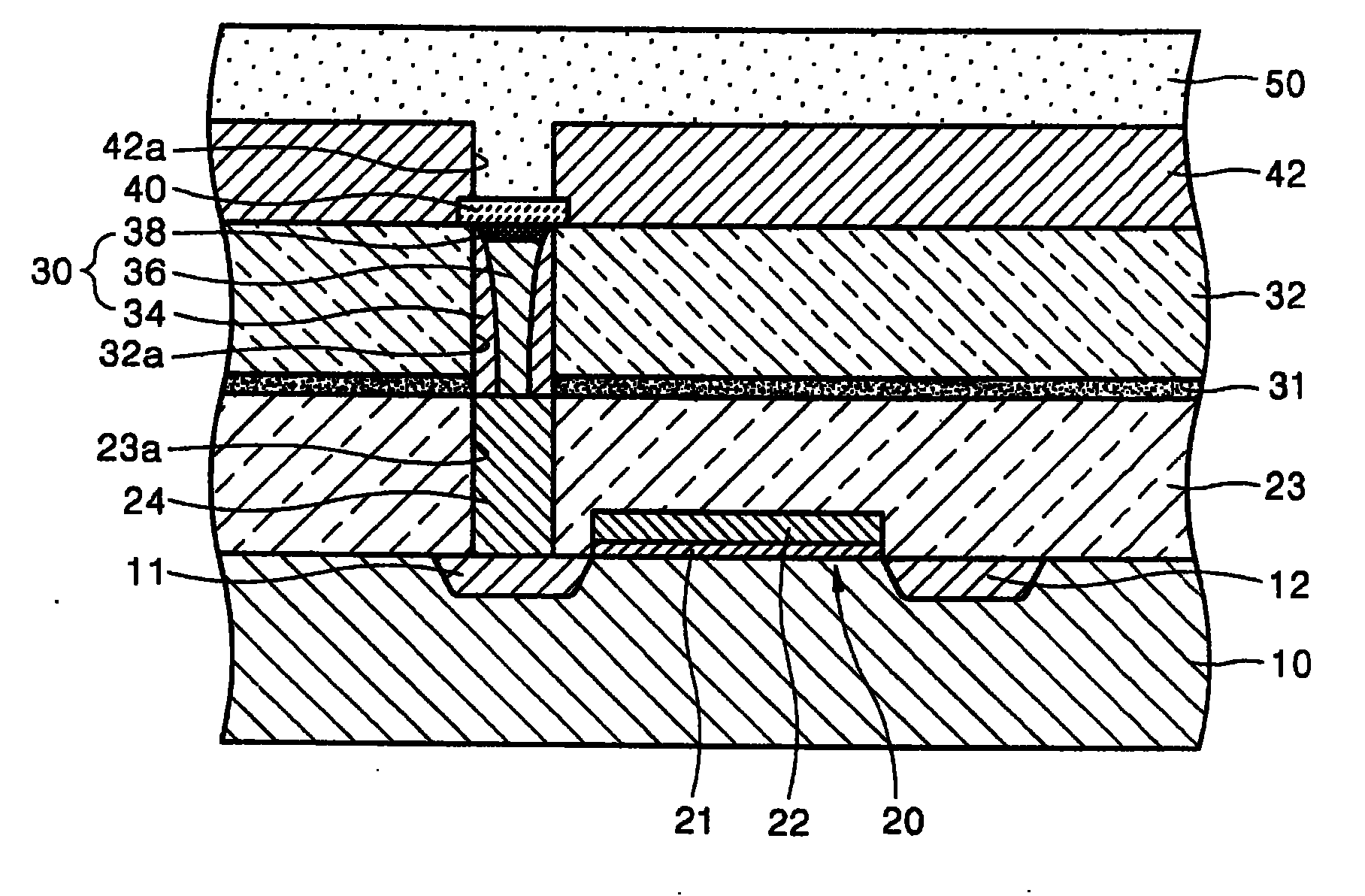
图2是根据本发明一优选实施方式的半导体存储器件的剖视图;2 is a cross-sectional view of a semiconductor memory device according to a preferred embodiment of the present invention;
图3是曲线图,示出当利用原子层沉积工艺形成TiAlN层时,TiAlN的根据温度和氧化而变的电阻;3 is a graph showing resistance of TiAlN as a function of temperature and oxidation when a TiAlN layer is formed using an atomic layer deposition process;
图4是根据本发明另一优选实施方式的半导体器件的剖视图,其是图2所示半导体存储器件的改型;以及4 is a cross-sectional view of a semiconductor device according to another preferred embodiment of the present invention, which is a modification of the semiconductor memory device shown in FIG. 2; and
图5A到图5I是示出制造图4所示半导体存储器件的方法的剖视图。5A to 5I are cross-sectional views illustrating a method of manufacturing the semiconductor memory device shown in FIG. 4 .
具体实施方式 Detailed ways
下面将参照附图对本发明作更为全面的描述,附图示出了本发明的优选实施方式。The invention will now be described more fully with reference to the accompanying drawings, which show preferred embodiments of the invention.
图2是根据本发明一优选实施方式的半导体存储器件的剖视图。FIG. 2 is a cross-sectional view of a semiconductor memory device according to a preferred embodiment of the present invention.
参见图2,该半导体存储器件包括开关晶体管20、数据存储部分40、以及加热部分30,该加热部分加热数据存储部分40。晶体管20包括源极区11和漏极区12,源极区11和漏极区12是形成在p型硅基底(siliconesubstrate)上彼此隔开的n型(n+)层。栅极绝缘薄膜21和栅电极22形成在源极区11和漏极区12之间的基底10上。Referring to FIG. 2 , the semiconductor memory device includes a
数据存储部分40由硫属化物材料层形成,且传输外部信号的金属互连层50形成在硫属化物材料层上。硫属化物材料层40由三元相系统Te-Ge-Sb形成。The
加热部分30是本发明的特征所在,其被制在硫属化物材料层40的下方。加热部分30通过导电插塞24与晶体管20相连接。导电插塞24被制在一接触孔内,该接触孔被制在第一层间绝缘层23中,第一层间绝缘层23被制在基底10上以覆盖晶体管20。由于导电插塞24经由源极区11接收电流,并将电流输送给加热部分30,所以优选地用低电阻的钨制造导电插塞24。The
加热部分30被制在通孔32a中,该通孔32a被制在一第二层间绝缘层32中,该第二层间绝缘层沉积在第一层间绝缘层23上。在通孔30的内壁上制有隔离壁34。在隔离壁34内制有加热材料层36,其例如由氮化铝钛(TiAlN)制成。优选的是,利用一等离子氧化工艺对TiAlN层36的顶面进行氧化,从而形成预定的氧化物薄膜38,使得TiAlN层36的上部具有高电阻,而TiAlN层36的下部具有高电导率。The
金属互连层50经过通孔42a与硫属化物材料层40相连,其中的通孔42a被制在第三层间绝缘层42中,第三层间绝缘层被制在第二层间绝缘层32之上。The
附图标记31指代SiN薄膜,当通过对SiO2制成的第二层间绝缘层32执行湿蚀刻而形成通孔32a时,薄膜31可起到蚀刻阻挡层的作用。
图3是曲线图,示出当利用原子层沉积(ALD)工艺形成TiAlN层时,TiAlN的根据温度和氧化而变的电阻。FIG. 3 is a graph showing resistance of TiAlN according to temperature and oxidation when a TiAlN layer is formed using an atomic layer deposition (ALD) process.
参见图3,当作为Ti的前体(precursor)的TiCl4与作为Al的前体的Al(CH3)3相互发生反应时,两前体间的反应速度根据沉积温度而变,从而TiAl的成分出现改变。接着,NH3被吸附且氮化,从而形成TiAlN层。另外,随着TiAlN层成分改变,TiAlN层的电阻值发生变化。与此同时,由于利用等离子氧化工艺对TiAlN层的顶面进行了氧化,所以TiAlN层的电阻值急剧地增大100倍左右。Referring to Fig. 3, when TiCl 4 as a precursor of Ti and Al(CH 3 ) 3 as a precursor of Al react with each other, the reaction speed between the two precursors changes according to the deposition temperature, so that the TiAl Composition changes. Next, NH 3 is adsorbed and nitrided, thereby forming a TiAlN layer. In addition, as the composition of the TiAlN layer changes, the resistance value of the TiAlN layer changes. At the same time, since the top surface of the TiAlN layer is oxidized by the plasma oxidation process, the resistance value of the TiAlN layer increases sharply by about 100 times.
下面将参照附图对上述存储单元的工作过程进行详细描述。The working process of the above storage unit will be described in detail below with reference to the accompanying drawings.
例如,当向晶体管20的栅电极22施加电压时,晶体管20导通,使得电流在源极区11与漏极区12之间流动。相应地,电流经导电插塞24和加热材料层36而流入硫属化物材料层40中。此时,由于在加热材料层36下部电流密度增大,所以能容易地实现预热。由于加热材料层36的上部处发热量(heating value)很大,所以加热材料层36能将大量的热传递给硫属化物材料层40。此时,根据加热材料层36的发热量,硫属化物材料层40被转变为非晶态或晶态。也就是说,当晶体管20的导通时间长时,硫属化物材料层40转变成晶态,因而作为导电材料。相反,当晶体管的导通时间短时,硫属化物材料层40转变为非晶态,因而作为电阻材料。For example, when a voltage is applied to the
因此,利用相变过程,选择晶体管20和金属互连层50的存储单元,以写入数据“1”或“0”。另外,通过读取硫属化物材料层40的电阻可读出已写入的数据“1”或“0”。Therefore, using the phase change process, the memory cells of the
图4是根据本发明另一优选实施方式的半导体器件的剖视图,其是图2所示半导体存储器件的改型。图4中相同的附图标记表示与图2相同的元件,且将略去对这些元件的详细描述。4 is a cross-sectional view of a semiconductor device according to another preferred embodiment of the present invention, which is a modification of the semiconductor memory device shown in FIG. 2 . The same reference numerals in FIG. 4 denote the same elements as in FIG. 2 , and detailed descriptions of these elements will be omitted.
参见图4,以覆盖通孔42a的方式在第三层间绝缘层42上形成TiAlN薄膜51。利用等离子氧化工艺对TiAlN薄膜51的顶面进行氧化,使得防止了从硫属化物材料层40到金属互连层50传递的电热(electric heat)。Referring to FIG. 4, a TiAlN
图5A到图5I是示出制造图4所示半导体存储器件的方法的剖视图。5A to 5I are cross-sectional views illustrating a method of manufacturing the semiconductor memory device shown in FIG. 4 .
首先,如图5A所示,利用半导体领域公知的方法在半导体基底10上形成晶体管20。然后,在半导体基底10上形成第一层间绝缘层23。选择性地蚀刻第一层间绝缘层23,从而形成露出晶体管20的源极区11的接触孔23a。将导电插塞24填入到接触孔23a中,以使其与源极区11相连接。此处,导电插塞24由多晶硅或钨制成,优选用低电阻的钨制成。First, as shown in FIG. 5A , a
然后,如图5B所示,在第一层间绝缘层23上依次沉积SiN制成的绝缘薄膜31、以及第二层间绝缘层32,该绝缘薄膜31覆盖导电插塞24。选择性地蚀刻绝缘层31和第二层间绝缘层32,从而形成露出导电插塞24的通孔32a。Then, as shown in FIG. 5B , an insulating
而后,如图5C所示,在第二层间绝缘层32上形成例如由SiN制成的绝缘薄膜33,从而覆盖通孔32a的内壁。Then, as shown in FIG. 5C, an insulating
然后,如图5D所示,对绝缘薄膜33执行离子蚀刻,直到第二层间绝缘层32从绝缘薄膜33的顶部露出为止。利用离子蚀刻工艺对形成在通孔32a内壁上的绝缘薄膜33执行蚀刻,从而形成底部大且顶部小的隔离壁34。Then, as shown in FIG. 5D , ion etching is performed on the insulating
然后,如图5E所示,利用ALD工艺在第二层间绝缘层32上沉积TiAlN薄膜35,从而填充通孔32a中的隔离壁34。此处,使用ALD工艺沉积TiAlN薄膜35的原因在于:通过调整沉积温度可对TiAlN的组成成分进行控制,进而能如图3所示那样对其电阻进行控制。Then, as shown in FIG. 5E, a TiAlN
之后,如图5F所示,利用化学机械抛光(CMP)平坦化TiAlN薄膜35,从而暴露出第二层间绝缘层32,并由此形成加热材料层36。利用等离子氧化工艺对加热材料层36的顶面执行氧化,从而形成氧化物薄膜38。如图3所示,其上形成氧化物薄膜38的加热材料层36的电阻急剧增大。结果就是,尽管所通过的电流不变,但发热量却增大了。Afterwards, as shown in FIG. 5F , the
而后,如图5G所示,在第二层间绝缘层32和加热材料层36上溅镀三元相系统Te-Ge-Sb,从而形成硫属化物薄膜。然后,构图硫属化物薄膜,从而在加热材料层36上形成硫属化物材料层40。Then, as shown in FIG. 5G , the ternary phase system Te—Ge—Sb is sputtered on the second
之后,还如图5G所示那样,在第二层间绝缘层32上形成第三层间绝缘层42,以覆盖硫属化物材料层40。然后,为了露出硫属化物材料层40,在第三层间绝缘层42中形成通孔42a。After that, as shown in FIG. 5G , a third
然后,如图5H所示,利用ALD工艺在第三层间绝缘层42上沉积TiAlN薄膜51,从而覆盖通孔42a。然后,利用等离子氧化工艺对TiAlN薄膜51的顶面执行氧化。氧化后的TiAlN薄膜51防止了电热从硫属化物材料40传递到金属互连层50中,下文将对金属互连层50进行介绍。Then, as shown in FIG. 5H , a
而后,如图5I所示,在TiAlN薄膜51上形成金属互连层50,其用TiAlN或钨制成。金属互连层50被制成格栅状(shape of a grid),从而向硫属化物材料层40传输外部信号,该硫属化物材料层40为所选定存储单元的数据存储部分。Then, as shown in FIG. 5I, a
如上所述,在根据本发明的半导体存储器件中,加热材料层被布置在硫属化物材料层的下方,且利用等离子氧化工艺对加热材料层的顶面执行氧化,以增大电阻值。因而,利用小的电流就能向硫属化物材料层输送其所必需的热量,从而可减小该半导体存储器件所用的电流。As described above, in the semiconductor memory device according to the present invention, the heating material layer is disposed under the chalcogenide material layer, and oxidation is performed on the top surface of the heating material layer using a plasma oxidation process to increase the resistance value. Therefore, the necessary heat can be delivered to the chalcogenide material layer with a small current, so that the current used by the semiconductor memory device can be reduced.
尽管已经结合示例性的实施方式对本发明作了特定的表示和描述,但本领域普通技术人员可以领会,在不悖离由所附权利要求书所限定的本发明的设计思想和保护范围的前提下,可对本发明的具体形式和细节进行各种改动。Although the present invention has been specifically shown and described in conjunction with exemplary embodiments, those of ordinary skill in the art can understand that without departing from the premise of the design idea and protection scope of the present invention defined by the appended claims Various changes may be made in the specific form and details of the present invention below.
Claims (14)
Applications Claiming Priority (3)
| Application Number | Priority Date | Filing Date | Title |
|---|---|---|---|
| KR32882/2003 | 2003-05-23 | ||
| KR32882/03 | 2003-05-23 | ||
| KR1020030032882A KR100979710B1 (en) | 2003-05-23 | 2003-05-23 | Semiconductor memory device and manufacturing method |
Publications (2)
| Publication Number | Publication Date |
|---|---|
| CN1574410A CN1574410A (en) | 2005-02-02 |
| CN100435373C true CN100435373C (en) | 2008-11-19 |
Family
ID=33095679
Family Applications (1)
| Application Number | Title | Priority Date | Filing Date |
|---|---|---|---|
| CNB2004100343559A Expired - Fee Related CN100435373C (en) | 2003-05-23 | 2004-04-12 | Semiconductor memory device and manufacturing method thereof |
Country Status (6)
| Country | Link |
|---|---|
| US (2) | US7164147B2 (en) |
| EP (1) | EP1480273B1 (en) |
| JP (1) | JP4813027B2 (en) |
| KR (1) | KR100979710B1 (en) |
| CN (1) | CN100435373C (en) |
| DE (1) | DE602004013489D1 (en) |
Families Citing this family (156)
| Publication number | Priority date | Publication date | Assignee | Title |
|---|---|---|---|---|
| US7893419B2 (en) | 2003-08-04 | 2011-02-22 | Intel Corporation | Processing phase change material to improve programming speed |
| KR100629265B1 (en) * | 2004-08-04 | 2006-09-29 | 삼성전자주식회사 | A method of forming a conductive layer having a local high resistance region and a semiconductor device manufactured using the same |
| TW200620473A (en) * | 2004-09-08 | 2006-06-16 | Renesas Tech Corp | Nonvolatile memory device |
| KR100738070B1 (en) * | 2004-11-06 | 2007-07-12 | 삼성전자주식회사 | Nonvolatile Memory Device with One Resistor and One Transistor |
| CN100461482C (en) * | 2004-11-17 | 2009-02-11 | 株式会社东芝 | Switching elements, line switching devices and logic circuits |
| JP4783045B2 (en) * | 2004-11-17 | 2011-09-28 | 株式会社東芝 | Switching element |
| KR100827653B1 (en) * | 2004-12-06 | 2008-05-07 | 삼성전자주식회사 | Phase change memory cells and manufacturing methods thereof |
| DE102004059428A1 (en) | 2004-12-09 | 2006-06-22 | Infineon Technologies Ag | Manufacturing method for a microelectronic electrode structure, in particular for a PCM memory element, and corresponding microelectronic electrode structure |
| KR100618879B1 (en) | 2004-12-27 | 2006-09-01 | 삼성전자주식회사 | Germanium precursor, UST thin film formed using the same, method for manufacturing the thin film and phase change memory device |
| KR100604923B1 (en) * | 2005-01-04 | 2006-07-28 | 삼성전자주식회사 | Method for forming titanium aluminum nitride film by atomic layer deposition method and phase change memory device having a heating electrode manufactured using the same |
| US20060169968A1 (en) * | 2005-02-01 | 2006-08-03 | Thomas Happ | Pillar phase change memory cell |
| JP4591821B2 (en) * | 2005-02-09 | 2010-12-01 | エルピーダメモリ株式会社 | Semiconductor device |
| KR100688532B1 (en) | 2005-02-14 | 2007-03-02 | 삼성전자주식회사 | Tellurium precursor, Te-containing chalcogenide thin film manufactured using the same, method for manufacturing the thin film and phase change memory device |
| JP5474272B2 (en) * | 2005-03-15 | 2014-04-16 | ピーエスフォー ルクスコ エスエイアールエル | Memory device and manufacturing method thereof |
| JP2006352082A (en) * | 2005-05-19 | 2006-12-28 | Renesas Technology Corp | Semiconductor memory device and manufacturing method thereof |
| KR100650752B1 (en) * | 2005-06-10 | 2006-11-27 | 주식회사 하이닉스반도체 | Phase change memory device and manufacturing method thereof |
| US20060284156A1 (en) * | 2005-06-16 | 2006-12-21 | Thomas Happ | Phase change memory cell defined by imprint lithography |
| KR100642645B1 (en) * | 2005-07-01 | 2006-11-10 | 삼성전자주식회사 | Memory device having a highly integrated cell structure and manufacturing method thereof |
| KR100625170B1 (en) | 2005-07-13 | 2006-09-15 | 삼성전자주식회사 | Electrode structure, manufacturing method thereof, phase change memory device including same and manufacturing method thereof |
| JP4560818B2 (en) | 2005-07-22 | 2010-10-13 | エルピーダメモリ株式会社 | Semiconductor device and manufacturing method thereof |
| KR100682969B1 (en) * | 2005-08-04 | 2007-02-15 | 삼성전자주식회사 | Phase change material, phase change ram including the same and method of manufacturing and operating the same |
| KR100655440B1 (en) | 2005-08-30 | 2006-12-08 | 삼성전자주식회사 | Phase change memory device and its formation method |
| EP1764837B1 (en) * | 2005-09-14 | 2009-08-05 | STMicroelectronics S.r.l. | Method of manufacturing a phase change memory device having a uniform heater height |
| US7589364B2 (en) * | 2005-11-02 | 2009-09-15 | Elpida Memory, Inc. | Electrically rewritable non-volatile memory element and method of manufacturing the same |
| US7541607B2 (en) * | 2005-11-02 | 2009-06-02 | Elpida Memory, Inc. | Electrically rewritable non-volatile memory element and method of manufacturing the same |
| US7786460B2 (en) | 2005-11-15 | 2010-08-31 | Macronix International Co., Ltd. | Phase change memory device and manufacturing method |
| US7635855B2 (en) * | 2005-11-15 | 2009-12-22 | Macronix International Co., Ltd. | I-shaped phase change memory cell |
| US7450411B2 (en) * | 2005-11-15 | 2008-11-11 | Macronix International Co., Ltd. | Phase change memory device and manufacturing method |
| US7394088B2 (en) | 2005-11-15 | 2008-07-01 | Macronix International Co., Ltd. | Thermally contained/insulated phase change memory device and method (combined) |
| US7414258B2 (en) | 2005-11-16 | 2008-08-19 | Macronix International Co., Ltd. | Spacer electrode small pin phase change memory RAM and manufacturing method |
| US7449710B2 (en) * | 2005-11-21 | 2008-11-11 | Macronix International Co., Ltd. | Vacuum jacket for phase change memory element |
| US7829876B2 (en) | 2005-11-21 | 2010-11-09 | Macronix International Co., Ltd. | Vacuum cell thermal isolation for a phase change memory device |
| US7599217B2 (en) * | 2005-11-22 | 2009-10-06 | Macronix International Co., Ltd. | Memory cell device and manufacturing method |
| JP4860249B2 (en) * | 2005-11-26 | 2012-01-25 | エルピーダメモリ株式会社 | Phase change memory device and method of manufacturing phase change memory device |
| US7688619B2 (en) | 2005-11-28 | 2010-03-30 | Macronix International Co., Ltd. | Phase change memory cell and manufacturing method |
| US7459717B2 (en) | 2005-11-28 | 2008-12-02 | Macronix International Co., Ltd. | Phase change memory cell and manufacturing method |
| US7521364B2 (en) * | 2005-12-02 | 2009-04-21 | Macronix Internation Co., Ltd. | Surface topology improvement method for plug surface areas |
| TWI319233B (en) * | 2005-12-19 | 2010-01-01 | Macronix Int Co Ltd | Phase change memory cell and manufacturing method |
| US7531825B2 (en) * | 2005-12-27 | 2009-05-12 | Macronix International Co., Ltd. | Method for forming self-aligned thermal isolation cell for a variable resistance memory array |
| US8062833B2 (en) | 2005-12-30 | 2011-11-22 | Macronix International Co., Ltd. | Chalcogenide layer etching method |
| KR100695166B1 (en) * | 2006-01-03 | 2007-03-14 | 삼성전자주식회사 | Method for manufacturing a phase change memory device having a fullerene layer |
| US7595218B2 (en) | 2006-01-09 | 2009-09-29 | Macronix International Co., Ltd. | Programmable resistive RAM and manufacturing method |
| US7741636B2 (en) | 2006-01-09 | 2010-06-22 | Macronix International Co., Ltd. | Programmable resistive RAM and manufacturing method |
| US7560337B2 (en) * | 2006-01-09 | 2009-07-14 | Macronix International Co., Ltd. | Programmable resistive RAM and manufacturing method |
| JP4591833B2 (en) * | 2006-01-17 | 2010-12-01 | エルピーダメモリ株式会社 | Phase change memory device and method of manufacturing phase change memory device |
| JP4691454B2 (en) * | 2006-02-25 | 2011-06-01 | エルピーダメモリ株式会社 | Phase change memory device and manufacturing method thereof |
| US7324365B2 (en) * | 2006-03-02 | 2008-01-29 | Infineon Technologies Ag | Phase change memory fabricated using self-aligned processing |
| US7514705B2 (en) * | 2006-04-25 | 2009-04-07 | International Business Machines Corporation | Phase change memory cell with limited switchable volume |
| CN100459049C (en) * | 2006-04-28 | 2009-02-04 | 台湾薄膜电晶体液晶显示器产业协会 | Method for manufacturing active layer film by using precursor solution of metal-chalcogenide compound |
| US8129706B2 (en) * | 2006-05-05 | 2012-03-06 | Macronix International Co., Ltd. | Structures and methods of a bistable resistive random access memory |
| US7608848B2 (en) * | 2006-05-09 | 2009-10-27 | Macronix International Co., Ltd. | Bridge resistance random access memory device with a singular contact structure |
| US7494841B2 (en) * | 2006-05-12 | 2009-02-24 | International Business Machines Corporation | Solution-based deposition process for metal chalcogenides |
| US8618523B2 (en) | 2006-05-31 | 2013-12-31 | Renesas Electronics Corporation | Semiconductor device |
| US7696506B2 (en) * | 2006-06-27 | 2010-04-13 | Macronix International Co., Ltd. | Memory cell with memory material insulation and manufacturing method |
| US7750333B2 (en) * | 2006-06-28 | 2010-07-06 | Intel Corporation | Bit-erasing architecture for seek-scan probe (SSP) memory storage |
| US7785920B2 (en) | 2006-07-12 | 2010-08-31 | Macronix International Co., Ltd. | Method for making a pillar-type phase change memory element |
| JP2008053494A (en) * | 2006-08-25 | 2008-03-06 | Elpida Memory Inc | Semiconductor device and manufacturing method thereof |
| JP4437299B2 (en) | 2006-08-25 | 2010-03-24 | エルピーダメモリ株式会社 | Semiconductor device and manufacturing method thereof |
| JP2008060541A (en) * | 2006-08-29 | 2008-03-13 | Korea Electronics Telecommun | Method of manufacturing a phase change memory device having a GST chalcogenide pattern |
| US7772581B2 (en) * | 2006-09-11 | 2010-08-10 | Macronix International Co., Ltd. | Memory device having wide area phase change element and small electrode contact area |
| JP4267013B2 (en) | 2006-09-12 | 2009-05-27 | エルピーダメモリ株式会社 | Manufacturing method of semiconductor device |
| KR100807230B1 (en) | 2006-09-27 | 2008-02-28 | 삼성전자주식회사 | Phase change material layer and phase change memory device including the same |
| KR100766504B1 (en) * | 2006-09-29 | 2007-10-15 | 삼성전자주식회사 | Semiconductor device and manufacturing method thereof |
| US7504653B2 (en) * | 2006-10-04 | 2009-03-17 | Macronix International Co., Ltd. | Memory cell device with circumferentially-extending memory element |
| CN100461484C (en) * | 2006-10-13 | 2009-02-11 | 中国科学院上海微系统与信息技术研究所 | Phase-change memory storage unit and preparation method thereof |
| KR100858083B1 (en) * | 2006-10-18 | 2008-09-10 | 삼성전자주식회사 | A phase change memory device having a large contact area between a lower electrode contact layer and a phase change layer and a method of manufacturing the same |
| US7863655B2 (en) | 2006-10-24 | 2011-01-04 | Macronix International Co., Ltd. | Phase change memory cells with dual access devices |
| US8067762B2 (en) | 2006-11-16 | 2011-11-29 | Macronix International Co., Ltd. | Resistance random access memory structure for enhanced retention |
| US7473576B2 (en) * | 2006-12-06 | 2009-01-06 | Macronix International Co., Ltd. | Method for making a self-converged void and bottom electrode for memory cell |
| US7682868B2 (en) * | 2006-12-06 | 2010-03-23 | Macronix International Co., Ltd. | Method for making a keyhole opening during the manufacture of a memory cell |
| US7476587B2 (en) | 2006-12-06 | 2009-01-13 | Macronix International Co., Ltd. | Method for making a self-converged memory material element for memory cell |
| US7903447B2 (en) | 2006-12-13 | 2011-03-08 | Macronix International Co., Ltd. | Method, apparatus and computer program product for read before programming process on programmable resistive memory cell |
| US7718989B2 (en) * | 2006-12-28 | 2010-05-18 | Macronix International Co., Ltd. | Resistor random access memory cell device |
| US7619311B2 (en) * | 2007-02-02 | 2009-11-17 | Macronix International Co., Ltd. | Memory cell device with coplanar electrode surface and method |
| US7884343B2 (en) * | 2007-02-14 | 2011-02-08 | Macronix International Co., Ltd. | Phase change memory cell with filled sidewall memory element and method for fabricating the same |
| US7956344B2 (en) * | 2007-02-27 | 2011-06-07 | Macronix International Co., Ltd. | Memory cell with memory element contacting ring-shaped upper end of bottom electrode |
| KR100858089B1 (en) * | 2007-03-06 | 2008-09-10 | 삼성전자주식회사 | Phase change memory device, manufacturing and operation method thereof |
| US7786461B2 (en) * | 2007-04-03 | 2010-08-31 | Macronix International Co., Ltd. | Memory structure with reduced-size memory element between memory material portions |
| US7569844B2 (en) | 2007-04-17 | 2009-08-04 | Macronix International Co., Ltd. | Memory cell sidewall contacting side electrode |
| US7940552B2 (en) * | 2007-04-30 | 2011-05-10 | Samsung Electronics Co., Ltd. | Multiple level cell phase-change memory device having pre-reading operation resistance drift recovery, memory systems employing such devices and methods of reading memory devices |
| KR100914267B1 (en) * | 2007-06-20 | 2009-08-27 | 삼성전자주식회사 | Variable resistance memory device and its formation method |
| KR100881055B1 (en) | 2007-06-20 | 2009-01-30 | 삼성전자주식회사 | Phase change memory unit, manufacturing method thereof, phase change memory device including same and manufacturing method thereof |
| KR100875165B1 (en) * | 2007-07-04 | 2008-12-22 | 주식회사 동부하이텍 | Semiconductor device and manufacturing method |
| KR101308549B1 (en) * | 2007-07-12 | 2013-09-13 | 삼성전자주식회사 | Multi-level phase change memory device and write method thereof |
| TWI402980B (en) | 2007-07-20 | 2013-07-21 | Macronix Int Co Ltd | Resistive memory structure with buffer layer |
| KR101258268B1 (en) * | 2007-07-26 | 2013-04-25 | 삼성전자주식회사 | NAND-type resistive memory cell strings of a non-volatile memory device and methods of fabricating the same |
| US7729161B2 (en) | 2007-08-02 | 2010-06-01 | Macronix International Co., Ltd. | Phase change memory with dual word lines and source lines and method of operating same |
| US7642125B2 (en) * | 2007-09-14 | 2010-01-05 | Macronix International Co., Ltd. | Phase change memory cell in via array with self-aligned, self-converged bottom electrode and method for manufacturing |
| US8178386B2 (en) | 2007-09-14 | 2012-05-15 | Macronix International Co., Ltd. | Phase change memory cell array with self-converged bottom electrode and method for manufacturing |
| US7755074B2 (en) * | 2007-10-12 | 2010-07-13 | Ovonyx, Inc. | Low area contact phase-change memory |
| JP2009099854A (en) * | 2007-10-18 | 2009-05-07 | Elpida Memory Inc | Method of manufacturing vertical phase change memory device |
| US7919766B2 (en) | 2007-10-22 | 2011-04-05 | Macronix International Co., Ltd. | Method for making self aligning pillar memory cell device |
| US7646631B2 (en) * | 2007-12-07 | 2010-01-12 | Macronix International Co., Ltd. | Phase change memory cell having interface structures with essentially equal thermal impedances and manufacturing methods |
| KR101198100B1 (en) | 2007-12-11 | 2012-11-09 | 삼성전자주식회사 | Method of forming a phase-change material layer pattern, method of manufacturing a phase-change memory device and slurry composition used for the methods |
| US7639527B2 (en) | 2008-01-07 | 2009-12-29 | Macronix International Co., Ltd. | Phase change memory dynamic resistance test and manufacturing methods |
| US7879643B2 (en) | 2008-01-18 | 2011-02-01 | Macronix International Co., Ltd. | Memory cell with memory element contacting an inverted T-shaped bottom electrode |
| US7879645B2 (en) * | 2008-01-28 | 2011-02-01 | Macronix International Co., Ltd. | Fill-in etching free pore device |
| US8158965B2 (en) | 2008-02-05 | 2012-04-17 | Macronix International Co., Ltd. | Heating center PCRAM structure and methods for making |
| US8084842B2 (en) * | 2008-03-25 | 2011-12-27 | Macronix International Co., Ltd. | Thermally stabilized electrode structure |
| US8030634B2 (en) | 2008-03-31 | 2011-10-04 | Macronix International Co., Ltd. | Memory array with diode driver and method for fabricating the same |
| US7825398B2 (en) | 2008-04-07 | 2010-11-02 | Macronix International Co., Ltd. | Memory cell having improved mechanical stability |
| US7791057B2 (en) * | 2008-04-22 | 2010-09-07 | Macronix International Co., Ltd. | Memory cell having a buried phase change region and method for fabricating the same |
| US8077505B2 (en) * | 2008-05-07 | 2011-12-13 | Macronix International Co., Ltd. | Bipolar switching of phase change device |
| US7701750B2 (en) | 2008-05-08 | 2010-04-20 | Macronix International Co., Ltd. | Phase change device having two or more substantial amorphous regions in high resistance state |
| KR100981736B1 (en) * | 2008-05-23 | 2010-09-13 | 한국전자통신연구원 | Phase change memory device and manufacturing method thereof |
| US8415651B2 (en) * | 2008-06-12 | 2013-04-09 | Macronix International Co., Ltd. | Phase change memory cell having top and bottom sidewall contacts |
| US8134857B2 (en) * | 2008-06-27 | 2012-03-13 | Macronix International Co., Ltd. | Methods for high speed reading operation of phase change memory and device employing same |
| US20100019215A1 (en) * | 2008-07-22 | 2010-01-28 | Macronix International Co., Ltd. | Mushroom type memory cell having self-aligned bottom electrode and diode access device |
| US7932506B2 (en) | 2008-07-22 | 2011-04-26 | Macronix International Co., Ltd. | Fully self-aligned pore-type memory cell having diode access device |
| US7903457B2 (en) * | 2008-08-19 | 2011-03-08 | Macronix International Co., Ltd. | Multiple phase change materials in an integrated circuit for system on a chip application |
| US7719913B2 (en) * | 2008-09-12 | 2010-05-18 | Macronix International Co., Ltd. | Sensing circuit for PCRAM applications |
| US8324605B2 (en) * | 2008-10-02 | 2012-12-04 | Macronix International Co., Ltd. | Dielectric mesh isolated phase change structure for phase change memory |
| US7897954B2 (en) | 2008-10-10 | 2011-03-01 | Macronix International Co., Ltd. | Dielectric-sandwiched pillar memory device |
| US8036014B2 (en) * | 2008-11-06 | 2011-10-11 | Macronix International Co., Ltd. | Phase change memory program method without over-reset |
| US8664689B2 (en) | 2008-11-07 | 2014-03-04 | Macronix International Co., Ltd. | Memory cell access device having a pn-junction with polycrystalline plug and single-crystal semiconductor regions |
| US8907316B2 (en) * | 2008-11-07 | 2014-12-09 | Macronix International Co., Ltd. | Memory cell access device having a pn-junction with polycrystalline and single crystal semiconductor regions |
| KR20100060323A (en) * | 2008-11-27 | 2010-06-07 | 삼성전자주식회사 | Resistance variable memory device and method for forming the same |
| US7869270B2 (en) | 2008-12-29 | 2011-01-11 | Macronix International Co., Ltd. | Set algorithm for phase change memory cell |
| US8089137B2 (en) * | 2009-01-07 | 2012-01-03 | Macronix International Co., Ltd. | Integrated circuit memory with single crystal silicon on silicide driver and manufacturing method |
| US8107283B2 (en) * | 2009-01-12 | 2012-01-31 | Macronix International Co., Ltd. | Method for setting PCRAM devices |
| US8030635B2 (en) * | 2009-01-13 | 2011-10-04 | Macronix International Co., Ltd. | Polysilicon plug bipolar transistor for phase change memory |
| US8064247B2 (en) | 2009-01-14 | 2011-11-22 | Macronix International Co., Ltd. | Rewritable memory device based on segregation/re-absorption |
| US8933536B2 (en) | 2009-01-22 | 2015-01-13 | Macronix International Co., Ltd. | Polysilicon pillar bipolar transistor with self-aligned memory element |
| US8084760B2 (en) | 2009-04-20 | 2011-12-27 | Macronix International Co., Ltd. | Ring-shaped electrode and manufacturing method for same |
| US8173987B2 (en) * | 2009-04-27 | 2012-05-08 | Macronix International Co., Ltd. | Integrated circuit 3D phase change memory array and manufacturing method |
| US8097871B2 (en) | 2009-04-30 | 2012-01-17 | Macronix International Co., Ltd. | Low operational current phase change memory structures |
| US7933139B2 (en) * | 2009-05-15 | 2011-04-26 | Macronix International Co., Ltd. | One-transistor, one-resistor, one-capacitor phase change memory |
| US8350316B2 (en) | 2009-05-22 | 2013-01-08 | Macronix International Co., Ltd. | Phase change memory cells having vertical channel access transistor and memory plane |
| US7968876B2 (en) | 2009-05-22 | 2011-06-28 | Macronix International Co., Ltd. | Phase change memory cell having vertical channel access transistor |
| US8809829B2 (en) * | 2009-06-15 | 2014-08-19 | Macronix International Co., Ltd. | Phase change memory having stabilized microstructure and manufacturing method |
| US8406033B2 (en) | 2009-06-22 | 2013-03-26 | Macronix International Co., Ltd. | Memory device and method for sensing and fixing margin cells |
| US8363463B2 (en) | 2009-06-25 | 2013-01-29 | Macronix International Co., Ltd. | Phase change memory having one or more non-constant doping profiles |
| US8238149B2 (en) | 2009-06-25 | 2012-08-07 | Macronix International Co., Ltd. | Methods and apparatus for reducing defect bits in phase change memory |
| US8198619B2 (en) | 2009-07-15 | 2012-06-12 | Macronix International Co., Ltd. | Phase change memory cell structure |
| US7894254B2 (en) | 2009-07-15 | 2011-02-22 | Macronix International Co., Ltd. | Refresh circuitry for phase change memory |
| US8110822B2 (en) | 2009-07-15 | 2012-02-07 | Macronix International Co., Ltd. | Thermal protect PCRAM structure and methods for making |
| US8064248B2 (en) | 2009-09-17 | 2011-11-22 | Macronix International Co., Ltd. | 2T2R-1T1R mix mode phase change memory array |
| US8178387B2 (en) | 2009-10-23 | 2012-05-15 | Macronix International Co., Ltd. | Methods for reducing recrystallization time for a phase change material |
| US8729521B2 (en) | 2010-05-12 | 2014-05-20 | Macronix International Co., Ltd. | Self aligned fin-type programmable memory cell |
| US8310864B2 (en) | 2010-06-15 | 2012-11-13 | Macronix International Co., Ltd. | Self-aligned bit line under word line memory array |
| US8247789B2 (en) | 2010-08-31 | 2012-08-21 | Micron Technology, Inc. | Memory cells and methods of forming memory cells |
| US8395935B2 (en) | 2010-10-06 | 2013-03-12 | Macronix International Co., Ltd. | Cross-point self-aligned reduced cell size phase change memory |
| KR20130073038A (en) * | 2010-10-29 | 2013-07-02 | 휴렛-팩커드 디벨롭먼트 컴퍼니, 엘.피. | Memristive devices and memristors with ribbon-like junctions and methods for fabricating the same |
| US8497705B2 (en) | 2010-11-09 | 2013-07-30 | Macronix International Co., Ltd. | Phase change device for interconnection of programmable logic device |
| US8467238B2 (en) | 2010-11-15 | 2013-06-18 | Macronix International Co., Ltd. | Dynamic pulse operation for phase change memory |
| US8987700B2 (en) | 2011-12-02 | 2015-03-24 | Macronix International Co., Ltd. | Thermally confined electrode for programmable resistance memory |
| JP2014049497A (en) | 2012-08-29 | 2014-03-17 | Toshiba Corp | Nonvolatile semiconductor storage device and operation method of the same |
| JP5826779B2 (en) | 2013-02-27 | 2015-12-02 | 株式会社東芝 | Nonvolatile semiconductor memory device |
| TWI549229B (en) | 2014-01-24 | 2016-09-11 | 旺宏電子股份有限公司 | Multiple phase change materials in a memory device for system on a chip application |
| US9627612B2 (en) | 2014-02-27 | 2017-04-18 | International Business Machines Corporation | Metal nitride keyhole or spacer phase change memory cell structures |
| US9559113B2 (en) | 2014-05-01 | 2017-01-31 | Macronix International Co., Ltd. | SSL/GSL gate oxide in 3D vertical channel NAND |
| US9672906B2 (en) | 2015-06-19 | 2017-06-06 | Macronix International Co., Ltd. | Phase change memory with inter-granular switching |
| US10957587B2 (en) * | 2018-07-31 | 2021-03-23 | Taiwan Semiconductor Manufacturing Company, Ltd. | Structure and formation method of semiconductor device with conductive feature |
| WO2021092942A1 (en) * | 2019-11-15 | 2021-05-20 | 江苏时代全芯存储科技股份有限公司 | Memory unit and manufacturing method therefor |
| KR20220140257A (en) * | 2021-04-09 | 2022-10-18 | 에스케이하이닉스 주식회사 | Electronic device and method for fabricating the same |
| US12426277B2 (en) * | 2021-07-23 | 2025-09-23 | Taiwan Semiconductor Manufacturing Company, Ltd. | Embedded double side heating phase change random access memory (PCRAM) device and method of making same |
Citations (8)
| Publication number | Priority date | Publication date | Assignee | Title |
|---|---|---|---|---|
| US6072716A (en) * | 1999-04-14 | 2000-06-06 | Massachusetts Institute Of Technology | Memory structures and methods of making same |
| US20020058389A1 (en) * | 2000-09-29 | 2002-05-16 | Wicker Guy C. | Reduced contact area of sidewall conductor |
| CN1352808A (en) * | 1999-03-25 | 2002-06-05 | 能源变换设备有限公司 | Electrically programmable memory element with improved contacts |
| US20020080647A1 (en) * | 2000-12-21 | 2002-06-27 | Chien Chiang | Metal structure for a phase-change memory device |
| US20030003634A1 (en) * | 2001-06-30 | 2003-01-02 | Lowrey Tyler A. | Utilizing atomic layer deposition for programmable device |
| US20030036232A1 (en) * | 2000-12-14 | 2003-02-20 | Charles Dennison | Method to selectively increase the top resistance of the lower programming electrode in a phase-change memory. |
| US20030047727A1 (en) * | 2001-09-07 | 2003-03-13 | Chien Chiang | Using selective deposition to form phase-change memory cells |
| US6545903B1 (en) * | 2001-12-17 | 2003-04-08 | Texas Instruments Incorporated | Self-aligned resistive plugs for forming memory cell with phase change material |
Family Cites Families (18)
| Publication number | Priority date | Publication date | Assignee | Title |
|---|---|---|---|---|
| US6147395A (en) * | 1996-10-02 | 2000-11-14 | Micron Technology, Inc. | Method for fabricating a small area of contact between electrodes |
| US5825046A (en) * | 1996-10-28 | 1998-10-20 | Energy Conversion Devices, Inc. | Composite memory material comprising a mixture of phase-change memory material and dielectric material |
| US6969866B1 (en) * | 1997-10-01 | 2005-11-29 | Ovonyx, Inc. | Electrically programmable memory element with improved contacts |
| US6555860B2 (en) * | 2000-09-29 | 2003-04-29 | Intel Corporation | Compositionally modified resistive electrode |
| US6764894B2 (en) * | 2001-08-31 | 2004-07-20 | Ovonyx, Inc. | Elevated pore phase-change memory |
| JP4911845B2 (en) * | 2001-09-20 | 2012-04-04 | 株式会社リコー | Phase change nonvolatile memory element, memory array using the phase change nonvolatile memory element, and information recording method for the phase change nonvolatile memory element |
| JP2003100084A (en) * | 2001-09-27 | 2003-04-04 | Toshiba Corp | Phase change nonvolatile memory device |
| US6566700B2 (en) * | 2001-10-11 | 2003-05-20 | Ovonyx, Inc. | Carbon-containing interfacial layer for phase-change memory |
| EP1318552A1 (en) * | 2001-12-05 | 2003-06-11 | STMicroelectronics S.r.l. | Small area contact region, high efficiency phase change memory cell and fabrication method thereof |
| JP3948292B2 (en) * | 2002-02-01 | 2007-07-25 | 株式会社日立製作所 | Semiconductor memory device and manufacturing method thereof |
| US6707087B2 (en) * | 2002-06-21 | 2004-03-16 | Hewlett-Packard Development Company, L.P. | Structure of chalcogenide memory element |
| US6859382B2 (en) * | 2002-08-02 | 2005-02-22 | Unity Semiconductor Corporation | Memory array of a non-volatile ram |
| US6912146B2 (en) * | 2002-12-13 | 2005-06-28 | Ovonyx, Inc. | Using an MOS select gate for a phase change memory |
| US6869883B2 (en) * | 2002-12-13 | 2005-03-22 | Ovonyx, Inc. | Forming phase change memories |
| US7115927B2 (en) * | 2003-02-24 | 2006-10-03 | Samsung Electronics Co., Ltd. | Phase changeable memory devices |
| JP4254293B2 (en) * | 2003-03-25 | 2009-04-15 | 株式会社日立製作所 | Storage device |
| KR100504698B1 (en) * | 2003-04-02 | 2005-08-02 | 삼성전자주식회사 | Phase change memory device and method for forming the same |
| US6937507B2 (en) * | 2003-12-05 | 2005-08-30 | Silicon Storage Technology, Inc. | Memory device and method of operating same |
-
2003
- 2003-05-23 KR KR1020030032882A patent/KR100979710B1/en not_active Expired - Fee Related
-
2004
- 2004-03-12 EP EP04251445A patent/EP1480273B1/en not_active Expired - Lifetime
- 2004-03-12 DE DE602004013489T patent/DE602004013489D1/en not_active Expired - Lifetime
- 2004-04-12 CN CNB2004100343559A patent/CN100435373C/en not_active Expired - Fee Related
- 2004-05-06 US US10/839,261 patent/US7164147B2/en not_active Expired - Fee Related
- 2004-05-24 JP JP2004152661A patent/JP4813027B2/en not_active Expired - Fee Related
-
2007
- 2007-01-09 US US11/650,972 patent/US7501307B2/en not_active Expired - Lifetime
Patent Citations (8)
| Publication number | Priority date | Publication date | Assignee | Title |
|---|---|---|---|---|
| CN1352808A (en) * | 1999-03-25 | 2002-06-05 | 能源变换设备有限公司 | Electrically programmable memory element with improved contacts |
| US6072716A (en) * | 1999-04-14 | 2000-06-06 | Massachusetts Institute Of Technology | Memory structures and methods of making same |
| US20020058389A1 (en) * | 2000-09-29 | 2002-05-16 | Wicker Guy C. | Reduced contact area of sidewall conductor |
| US20030036232A1 (en) * | 2000-12-14 | 2003-02-20 | Charles Dennison | Method to selectively increase the top resistance of the lower programming electrode in a phase-change memory. |
| US20020080647A1 (en) * | 2000-12-21 | 2002-06-27 | Chien Chiang | Metal structure for a phase-change memory device |
| US20030003634A1 (en) * | 2001-06-30 | 2003-01-02 | Lowrey Tyler A. | Utilizing atomic layer deposition for programmable device |
| US20030047727A1 (en) * | 2001-09-07 | 2003-03-13 | Chien Chiang | Using selective deposition to form phase-change memory cells |
| US6545903B1 (en) * | 2001-12-17 | 2003-04-08 | Texas Instruments Incorporated | Self-aligned resistive plugs for forming memory cell with phase change material |
Also Published As
| Publication number | Publication date |
|---|---|
| KR100979710B1 (en) | 2010-09-02 |
| US20070108433A1 (en) | 2007-05-17 |
| US20040234895A1 (en) | 2004-11-25 |
| DE602004013489D1 (en) | 2008-06-19 |
| EP1480273B1 (en) | 2008-05-07 |
| JP4813027B2 (en) | 2011-11-09 |
| JP2004349709A (en) | 2004-12-09 |
| CN1574410A (en) | 2005-02-02 |
| EP1480273A2 (en) | 2004-11-24 |
| US7164147B2 (en) | 2007-01-16 |
| KR20040100499A (en) | 2004-12-02 |
| EP1480273A3 (en) | 2006-02-08 |
| US7501307B2 (en) | 2009-03-10 |
Similar Documents
| Publication | Publication Date | Title |
|---|---|---|
| KR100979710B1 (en) | Semiconductor memory device and manufacturing method | |
| KR100766504B1 (en) | Semiconductor device and manufacturing method thereof | |
| US7514704B2 (en) | Phase-change memory device and method of manufacturing the same | |
| JP4786136B2 (en) | Phase change memory element and method of forming the same | |
| CN102237390B (en) | Semiconductor device and manufacturing method thereof | |
| US8796101B2 (en) | Memory device | |
| US7704787B2 (en) | Methods for fabricating phase changeable memory devices | |
| US7397092B2 (en) | Phase changable memory device structures | |
| US8404514B2 (en) | Fabricating current-confining structures in phase change memory switch cells | |
| US8513051B2 (en) | Methods of forming phase-changeable memory devices including an adiabatic layer | |
| US20100072453A1 (en) | Phase-Changeable Fuse Elements and Memory Devices Containing Phase-Changeable Fuse Elements and Memory Cells Therein | |
| CN100559623C (en) | Non-volatile memory element and manufacture method thereof | |
| CN100541855C (en) | Non-volatile memory element and manufacture method thereof | |
| US20070246748A1 (en) | Phase change memory cell with limited switchable volume | |
| US20080075843A1 (en) | Method of Forming a Phase-Change Memory Unit and Method of Manufacturing a Phase-Change Memory Device Using the Same | |
| CN101877384B (en) | Low Operating Current Phase Change Memory Element Structure | |
| JP2008053494A (en) | Semiconductor device and manufacturing method thereof | |
| TW202032723A (en) | Method of manufacturing memory devices | |
| CN115362569A (en) | Phase change material switch and manufacturing method thereof | |
| US20060030108A1 (en) | Semiconductor device and method of fabricating the same | |
| KR20030081900A (en) | Method of fabricating Phase change Memory device | |
| US20240099168A1 (en) | Phase change memory cell | |
| KR100713943B1 (en) | Phase change memory device and manufacturing method thereof | |
| US12256653B2 (en) | PCM cell with nanoheater surrounded with airgaps | |
| US20240099164A1 (en) | Phase change memory cell |
Legal Events
| Date | Code | Title | Description |
|---|---|---|---|
| C06 | Publication | ||
| PB01 | Publication | ||
| C10 | Entry into substantive examination | ||
| SE01 | Entry into force of request for substantive examination | ||
| C14 | Grant of patent or utility model | ||
| GR01 | Patent grant | ||
| C17 | Cessation of patent right | ||
| CF01 | Termination of patent right due to non-payment of annual fee |
Granted publication date: 20081119 Termination date: 20140412 |