CN100383859C - Production process and production device of magnetic recording medium - Google Patents
Production process and production device of magnetic recording medium Download PDFInfo
- Publication number
- CN100383859C CN100383859C CNB2004800015656A CN200480001565A CN100383859C CN 100383859 C CN100383859 C CN 100383859C CN B2004800015656 A CNB2004800015656 A CN B2004800015656A CN 200480001565 A CN200480001565 A CN 200480001565A CN 100383859 C CN100383859 C CN 100383859C
- Authority
- CN
- China
- Prior art keywords
- mask layer
- layer
- mentioned
- processed
- magnetic recording
- Prior art date
- Legal status (The legal status is an assumption and is not a legal conclusion. Google has not performed a legal analysis and makes no representation as to the accuracy of the status listed.)
- Expired - Fee Related
Links
Images


Classifications
-
- G—PHYSICS
- G11—INFORMATION STORAGE
- G11B—INFORMATION STORAGE BASED ON RELATIVE MOVEMENT BETWEEN RECORD CARRIER AND TRANSDUCER
- G11B5/00—Recording by magnetisation or demagnetisation of a record carrier; Reproducing by magnetic means; Record carriers therefor
- G11B5/84—Processes or apparatus specially adapted for manufacturing record carriers
- G11B5/855—Coating only part of a support with a magnetic layer
Abstract
There is provided a process for efficiently producing a magnetic recording medium having good magnetic characteristics by suppressing deviation in the machining shape and magnetic deterioration of a split recording element. Ion beam etching is employed as a dry etching method of a continuous recording layer (20). A resist layer (26) is removed before dry etching the continuous recording layer (20). Diamond-like carbon is employed as the material of a first mask layer covering the continuous recording layer.
Description
Technical field
The present invention relates to the manufacture method and the manufacturing installation thereof of magnetic recording media.
Background technology
In the past, magnetic recording medias such as hard disk were along with the miniaturization of the magnetic particle that constitutes recording layer, the change of material, and improvement such as the miniaturization of magnetic head processing and area recording density is improved significantly expects still that from now on area recording density further improves.
Yet, problems such as the side interference that causes along with manufacturing limit and magnetic field broadening because of magnetic head, crosstalk become obvious, improvement before utilizing is held art and is improved area recording density and reach capacity, and the such suggestion of back benefit as the magnetic recording media that can realize further improving surface density of the discrete type magnetic recording media that continuous recording layer is divided into a plurality of cutting recording key elements as open shown in the flat 9-97419 communique the spy is for example arranged.
For example can utilize the spy as the process technology of cutting apart that realizes continuous recording layer and to open such ion beam milling shown in the flat 12-322710 communique.Contain NH with interpolation
3The CO (carbon monoxide) of nitrogen such as (ammonia) gas is the technology of the dry ecthings such as ion etching of reactant gas.
In addition, can use with the technology in the field of semiconductor manufacture such as photoetching of resist layer as the technology of the figure that the mask layer of dry ecthing is processed into regulation.
Summary of the invention
Yet, although technology with the dry ecthing of prior aries such as reactive ion etching, continuous recording layer can be divided into a plurality of cutting recording key elements with fine figure, but it is different or form the stage portion as the recess or form cutting recording key element that the side is a taper or in the certain deviation of generation between the machining shape of hope and the actual machining shape etc. because of the circumference of segmented element that the machining precision deviation of the cutting recording key element along with the position difference on the magnetic recording media often takes place.Because the deviation of the machining shape of such magnetic property deterioration and cutting recording key element, and often can not get the magnetic characteristic of wishing.
For example reactive ion etching has near the distribution of the plasma end of the processed body unsettled tendency that becomes, the tendency that has near the machining precision of the cutting recording key element end to reduce easily.
In addition, because need big bias power with CO (carbon monoxide) gas used etc. for the reactive ion etching of reactive gas in magnetic material processing, high temperature takes place in processed body easily, so the magnetic property deterioration often takes place because of the cutting recording key element is overheated.
In addition, though by the superheated that cooling body can prevent the cutting recording key element is set, but because the structure of manufacturing installation is thickened, cost is increased, there is near the distribution of the plasma periphery of processed body to become unsettled tendency simultaneously, so make temperature distributing disproportionation even easily, make the even cooling difficulty of processed body.
In addition, in order to improve the throughput rate of magnetic recording media, and preferably a plurality of processed bodies and row arrangement are processed simultaneously, but because cooling body generally comprises ESC (electrostatic chuck) and biasing printing mechanism, so and the occasion of a plurality of processed bodies of row arrangement, such cooling body is set, itself should along with space, machining precision etc. be not both the difficulty, cool off necessary reactive ion etching with processed body and handle a plurality of processed bodies simultaneously, make the magnetic recording media of discrete type criticize the production difficulty.
To this,, when using ion beam milling, there is the problem that forms stage portion easily along the circumference of cutting recording key element resemble the recess though can solve above problem with ion beam milling.
As illustrate in greater detail, then as shown in Figure 22 A, during the part in the mask 102 of I.B.M. from continuous recording layer 100, exposed, carry out removing of continuous recording layer 100 repeatedly, with the part of the particle of removing again attached on side 102A of mask 102 etc., though if the amount of attachment is few again, can remove one by one with ion beam, but, if amount for a long time, then just as shown in Figure 22 B, a part is deposited on the side 102A of mask 102, and the result will form stage portion 106 at the circumference of segmented element 104 as shown in Figure 22 C.Though it is this phenomenon is not obvious to dry corrosion, obvious especially in the ion beam erosion.In addition, the direction irradiation ion beam that tilts by the normal to a surface from processed relatively body in order to suppress this phenomenon etc. can be removed attachment more expeditiously from adding Ministry of worker side, this technology is known, but, be that fine occasion is not effective just at figure as if the magnetic recording media of discrete type as described above is such.
In addition, in the occasion with dry ecthing, as shown in Figure 23 A, formation side 200A is that the cutting recording key element 200 of subvertical ideal form is difficult, and in fact as shown in Figure 23 B, forming side 200A is the record key element 200 of taper.
If illustrate in greater detail, in dry ecthing, part gas tilts from the processed relatively body of vertical direction, and some are approaching, even expose from mask 202 end in etch target zone, also the approaching gas of relative tilt becomes the shadow region for mask, so be considered to carry out lately, the side 200A of cutting recording key element 200 be processed into taper than the etching of other parts.
The present invention proposes in view of following problem, provide can high-level efficiency manufacturing stop the deviation of the machining shape of cutting recording key element, the magnetic property deterioration and have the method for magnetic recording media of good magnetic characteristics and manufacturing installation as problem.
The present invention is by stoping near the decline of the machining precision of the continuous recording layer the end of processed body with ion beam milling as the dry etching technology of continuous recording layer, and the processing temperature of restriction continuous recording layer, prevents the magnetic property deterioration or the reduction of cutting recording key element.
In addition, the present invention comes to stop by the lining key element on the attenuate continuous recording layer formation of the stage portion of circumference by the resist layer on the mask layer of removing the lining continuous recording layer before the dry ecthing of continuous recording layer, the taper angle of cutting recording key element side improves the machining precision of cutting recording key element.
In addition, as the material of mask layer of lining continuous recording layer, preferably, be than being easier to the carbon that this puts employing adamas class than the control of low this point that also just can form thinly of ion beam milling and machining shape according to etch-rate.
At this, in this manual, this speech of the carbon of adamas class (hereinafter referred to as " DLC ") is to stipulate to be diamond lattic structure by being major component with carbon, shows with dimension formula hardness measurement 200~8000kgf/mm
2About the such implication of the material of hardness use.
In addition, in this manual, " ion beam milling " this speech is for example to use by the implication of the general name by Ionized gas being radiated at the job operation of removing on the processed body such as ion milling, is not limited to by concentrated ion Shu Jinhang and shines.
In addition, in this manual, " magnetic recording media " speech is not limited at recording of information, only use the hard disk of magnetic, soft (registered trade mark) disk, tape etc. in reading, and also comprises the magnetic recording media of the hot auxiliary type of MO Magnetooptic recording mediums such as (Magneto Optical), magnetic and heat and usefulness by magnetic and light and usefulness.
That is,, plan to solve above-mentioned problem by invention as described below.
(1) a kind of manufacture method of magnetic recording media, it is characterized in that, comprise following operation: (1) will form the processed body that continuous recording layer, mask layer and resist layer constitute in turn on substrate surface above-mentioned resist layer is processed into the resist layer manufacturing procedure of the graphics shape of regulation; (2) the aforementioned mask layer is processed into the mask layer manufacturing procedure of graphics shape according to the graphics shape of the resist layer after processed in operation (1); (3) remove the resist layer that remains in the resist layer on the aforementioned mask layer and remove operation; (4) according to the graphics shape of the mask layer after processed in operation (2), above-mentioned continuous recording layer is processed into graphics shape and is divided into the continuous recording layer manufacturing procedure of a plurality of cutting recording key elements by dry ecthing, the aforementioned mask layer is included in etch-rate 1st mask layer lower than above-mentioned continuous recording layer in the operation (4), and the etch-rate in operation (3) is lower and be configured in the 2nd mask layer between above-mentioned the 1st mask layer and the above-mentioned resist layer than above-mentioned the 1st mask layer, and operation (2) comprises following operation: (2A) graphics shape according to the resist layer after processed in operation (1) carries out the 2nd mask layer manufacturing procedure that graphics shape is processed in etching to above-mentioned the 2nd mask layer; (2B) above-mentioned the 1st mask layer is processed into the 1st mask layer manufacturing procedure of graphics shape, carries out operation (3) before in operation (4) according to the graphics shape of the 2nd mask layer after processed in operation (2A).
(2) as the manufacture method of (1) described magnetic recording media, it is characterized in that: above-mentioned the 1st mask layer forms thinly than above-mentioned continuous recording layer.
(3) as the manufacture method of (2) described magnetic recording media, it is characterized in that: the thickness t of above-mentioned the 1st mask layer is set at 3≤t≤15nm.
(4) as the manufacture method of (2) described magnetic recording media, it is characterized in that: the thickness t of above-mentioned the 1st mask layer is set at 3≤t≤10nm.
(5) as the manufacture method of (2) described magnetic recording media, it is characterized in that: the material of above-mentioned the 1st mask layer is set at diamond-like carbon.
(6) as the manufacture method of (3) described magnetic recording media, it is characterized in that: the material of above-mentioned the 1st mask layer is set at diamond-like carbon.
(7) as the manufacture method of (4) described magnetic recording media, it is characterized in that: the material of above-mentioned the 1st mask layer is set at diamond-like carbon.
(8) as the manufacture method of any one described magnetic recording media in (1) to (7), it is characterized in that: in operation (4), process above-mentioned continuous recording layer with ion beam milling.
(9) as the manufacture method of any one described magnetic recording media in (1) to (7), it is characterized in that: double the 1st mask layer manufacturing procedure (2B) of carrying out in operation (3).
(10) as the manufacture method of (9) described magnetic recording media, it is characterized in that: one of any removing for the reactive ion erosion agent of reacting gas remains in the resist layer on the 2nd mask layer after processed in operation (2A) in order to oxygen and ozone in operation (3), and according to the graphics shape of the 2nd mask layer after processed in operation (2A) the 1st mask layer is processed into graphics shape.
(11) as the manufacture method of (1) described magnetic recording media, it is characterized in that: the thickness of the 2nd mask layer material fully thin and/or the 2nd mask layer is the etch-rate material higher than the material of above-mentioned continuous recording layer in operation (4), so that in operation (4), remove and remain in the 2nd mask layer on the 1st mask layer after processed in operation (2B).
(12) as the manufacture method of (9) described magnetic recording media, it is characterized in that: the thickness of the 2nd mask layer material fully thin and/or the 2nd mask layer is the etch-rate material higher than the material of above-mentioned continuous recording layer in operation (4), so that in operation (4), remove and remain in the 2nd mask layer on the 1st mask layer after processed in operation (2B).
(13) as the manufacture method of (10) described magnetic recording media, it is characterized in that: the thickness of the 2nd mask layer material fully thin and/or the 2nd mask layer is the etch-rate material higher than the material of above-mentioned continuous recording layer in operation (4), so that in operation (4), remove and remain in the 2nd mask layer on the 1st mask layer after processed in operation (2B).
(14) as the manufacture method of (1) described magnetic recording media, it is characterized in that: the material of above-mentioned the 2nd mask layer is set at by at least one the silicon based material formed in the compound of silicon or silicon.
(15) as the manufacture method of (11) described magnetic recording media, it is characterized in that: the material of above-mentioned the 2nd mask layer is set at by at least one the silicon based material formed in the compound of silicon or silicon.
(16) as the manufacture method of (1) described magnetic recording media, it is characterized in that: in operation (2A), be that gas is that the reactive ion etching of reacting gas is processed above-mentioned the 2nd mask layer in order to fluorine.
(17) as the manufacture method of (9) described magnetic recording media, it is characterized in that: in operation (2A), be that gas is that the reactive ion etching of reacting gas is processed above-mentioned the 2nd mask layer in order to fluorine.
(18) as the manufacture method of (11) described magnetic recording media, it is characterized in that: in operation (2A), be that gas is that the reactive ion etching of reacting gas is processed above-mentioned the 2nd mask layer in order to fluorine.
(19) as the manufacture method of (14) described magnetic recording media, it is characterized in that: in operation (2A), be that gas is that the reactive ion etching of reacting gas is processed above-mentioned the 2nd mask layer in order to fluorine.
(20) as the manufacture method of any one described magnetic recording media in (1) to (7), it is characterized in that: in operation (1), process above-mentioned resist layer with stamping method.
(21) as the manufacture method of any one described magnetic recording media in (1) to (7), it is characterized in that: process a plurality of above-mentioned processed bodies simultaneously.
(22) a kind of manufacturing installation of magnetic recording media is characterized in that: comprise being used for carrying out as the processing unit (plant) of the manufacture method of (1) to (7) any one described magnetic recording media and be used for keeping simultaneously the maintenance anchor clamps of a plurality of above-mentioned processed bodies; Can process a plurality of above-mentioned processed bodies simultaneously.
(23) as the manufacturing installation of (22) described magnetic recording media, it is characterized in that: comprise the ion beam etching apparatus that is used to process above-mentioned continuous recording layer.
According to the present invention, can bring the magnetic property deterioration of deviation, the cutting recording key element of the machining shape that prevents the cutting recording key element, the such excellent results of recording medium of the good magnetic characteristic of high-level efficiency manufacturing really.
Description of drawings
Fig. 1 is pattern ground expression as the set out structure sectional side view of processed body of body of the processing of the magnetic recording media of embodiment of the present invention.
Fig. 2 is the sectional side view that the structure of the magnetic recording media that the processed body in the manuscript 1 obtains is represented on pattern ground.
Fig. 3 is the block scheme of structure of the manufacturing installation of the pattern ground expression recording medium that is used for manuscript 2.
Fig. 4 is the stereographic map that the structure of the retainer on the manufacturing installation among Fig. 3 represented to be equipped in summary.
Fig. 5 is the outboard profile that pattern ground expression is installed in the reactive ion etching device construction on the manufacturing installation among Fig. 3.
Fig. 6 is the outboard profile of the structure of the ion beam etching apparatus on the manufacturing installation in the pattern ground expression installation diagram 3.
Fig. 7 is the process flow diagram of the manufacturing process of expression magnetic recording media.
Fig. 8 is the sectional side view of pattern ground expression with the shape of the above-mentioned processed body of partition graph transcription on resist layer.
Fig. 9 is the sectional side view that the shape of the above-mentioned processed body behind the resist layer of groove bottom is removed in pattern ground expression.
Figure 10 is the sectional side view that the shape of the above-mentioned processed body behind the 2nd mask layer of recess bottom surface is removed in pattern ground expression.
Figure 11 is the sectional side view of shape of the above-mentioned processed body of pattern ground expression the 1st mask layer of removing groove bottom.
Figure 12 is the sectional side view of the shape of the pattern ground expression above-mentioned processed body that is formed with the cutting recording key element.
To be pattern ground expression remove the sectional side view of the shape of the above-mentioned processed body behind the 1st mask layer from the cutting recording key element to Figure 13.
Figure 14 be pattern be illustrated in the sectional side view of the shape of the processed body that is filled with nonmagnetic material between the cutting recording key element.
Figure 15 is the sectional side view of pattern ground expression with the shape of the processed body behind the flattening surface of cutting recording key element and nonmagnetic material.
Figure 16 is the microphotograph that the shape of the segmented element of the magnetic recording disk of embodiments of the invention is amplified expression.
Figure 17 is the magnetic recording disk of expression in Figure 16 and the curve of the distance of the end of the magnetic recording disk of comparative example and the relation of the etch-rate of continuous recording layer.
Figure 18 is the MFM picture of the magnetic recording disk among Figure 16.
Figure 19 is the MFM picture of the magnetic recording disk of comparative example 1.
Figure 20 is the microphotograph that the shape of the segmented element of the magnetic recording disk of comparative example 2 is amplified expression.
Figure 21 is the microphotograph that the shape of the segmented element of the magnetic recording disk of comparative example 3 is amplified expression.
Figure 22 A be pattern be expressed as the dry ecthing that utilizes prior art carry out continuous recording layer processing and with partly the be covered sectional side view of state of continuous recording layer of mask.
Figure 22 B be pattern be illustrated in the sectional side view of the build-up of particles process on the mask side among Figure 22.
Figure 22 C is the sectional side view of the stage portion of pattern ground established record key element of expression and circumference thereof.
Figure 23 A is the sectional side view of desirable forming process of the cutting recording key element of the pattern ground expression dry ecthing that utilizes prior art.
Figure 23 B is the sectional side view of actual forming process of the cutting recording key element of the pattern ground expression dry ecthing that utilizes prior art.
Embodiment
The contrast accompanying drawing describes preferred implementation of the present invention in detail below.
Present embodiment is about carry out processing such as dry ecthing on processed body such shown in the figure of the body that sets out as the processing of magnetic recording media, the shape of line and space diagram by continuous recording layer being processed into regulation such shown in Fig. 2 and the servo-actuated figure (not shown) that comprises contact hole is divided into the manufacture method of the magnetic recording media of a plurality of record key elements, not only on the process technology of continuous recording layer, and on the material of the mask layer of lining continuous recording layer, resistant layer and job operation thereof etc., also has feature.In addition, present embodiment is in the process technology that is used to implement these continuous recording layers, and the manufacturing installation of the magnetic recording media of batch production magnetic recording media has feature.With regard to other structure, since identical with manufacture method, the manufacturing installation of the magnetic recording media of prior art, so suitably omit explanation.
The material of bottom 14 is that the material of Cr (chromium) or evanohm, layer of soft magnetic material 16 is Fe (iron) alloy or Co (cobalt) alloy, and the material of oriented layer 18 is CoO, MgO, NiO etc., and the material of continuous recording layer 20 is Co (cobalt) alloys.In addition, the material of the 1st mask layer 22 is DLC, and the material of the 2nd mask layer 24 is Si (silicon), and resist layer is negative resist (a NEB22A Sumitomo Chemical Company Ltd system).
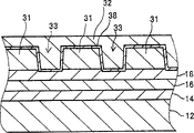
As shown in Figure 2; magnetic recording media 30 is disks of the discrete type of perpendicular recording type; above-mentioned continuous recording layer 20 is divided into a plurality of segmented elements 31 at the warp-wise of magnetic track with small interval; and filling nonmagnetic material 32 in the slot part 33 of 31 of cutting recording key elements forms protective seam 34 and lubricating layer 36 in turn on cutting recording key element 31 and nonmagnetic material 32.In addition, between cutting recording key element 31 and nonmagnetic material 32, form barrier film 38.
The material of nonmagnetic material 32 is SiO
2(silicon dioxide), the material of protective seam 34 and barrier film 38 are any above-mentioned hard carbon films that are called DLC, and the material of lubricating layer 36 is PFPE (PFPE).
As shown in Figure 3, the manufacturing installation 40 of magnetic recording media comprises: transcription means 42, lapping device 44, reactive ion etching device 46 and 48, ion beam etching apparatus 50, lapping device 52, dried cleaning device 54, barrier film form device 56, nonmagnetic material device for filling 58, planarizer 60, protection membrane formation device 62 and are used to form the lubricating layer formation device 64 of lubricating layer 36.
In addition, manufacturing installation 40 equipments are used to accommodate the vaccum retaining device 66 that burnishing device 44, reactive ion etching device 46,48, ion beam etching apparatus 50, burnishing device 52, dried cleaning device 54, barrier film formation device 56, nonmagnetic material device for filling 58, planarizer 60 and protective seam form device 62 and processed body remained on vacuum state.
In addition, manufacturing installation 40 comprises: the anchor clamps 68 that are used for keeping such shown in Fig. 4 of a plurality of processed bodies 10 simultaneously, transmit the not shown automatic conveyor of anchor clamps 68 automatically, can add a plurality of processed bodies 10 simultaneously.
Transcription means 42 is to use the model (not shown) that photoetching etc. is made to be pressed in that the back forms the device of the stamping method of groove on the resist layer 26 behind the figure of transcription regulation on the resist layer 26.
Burnishing device 44 with can by in removing with the polishing of oxygen, ozone or their gaseous plasma during printing the mode of the resist layer 26 of residual groove bottom constitute.
Reactive ion etching device 46 is can pass through with CF4 (4 fluorocarbons) gas or SF
6The mode that (sulfur hexafluoride) gas etc. are removed the 2nd mask layer 24 of groove bottom for the reactive ion etching of reactant gas constitutes.
Specifically, as shown in Figure 5, reactive ion etching device 46 is twin crystal bulk wave plasma modes, and comprises that diffusion cabin 46A is used for anchor clamps 68 are placed on the bell-jar 46C that ESC (electrostatic chuck) platform electrode 46B and being used in the diffuser casing produces the quartz system of plasma.
On ESC platform electrode 46B, connect the bias supply 46D that is used to apply bias voltage by electric wire.In addition, bias supply is that frequency is the AC power of 1.6MHz.
Quartzy system bell-jar 46C lower ending opening is in diffuser casing 46, and what be provided for supply response gas near the bottom gives pore 46E.Around quartz system bell-jar 46C, dispose solenoid 46F in addition, antenna 46G, plasma generation power supply 46H line is on antenna 46G.Plasma generation power supply 46H is that frequency is the AC power of 13.56MHz in addition.
The structure of reactive ion etching device 48 can not only be by being that reactive reactive ion etching is removed the resist layer 26 of groove with exterior domain with oxygen or ozone, and can remove the 1st mask layer of groove bottom.In addition, reactive ion etching device 48 and above-mentioned reactive ion etching device 46 are except that reactive kind is different, and structure is identical.
The structure of ion beam etching apparatus 50 can be divided into a plurality of cutting recording key elements 31 by removing the continuous recording layer 20 of groove bottom with the ion beam milling of Ar (argon) gas.
Specifically, ion beam etching apparatus 50, as shown in Figure 6, comprise vacuum chamber 50A, be used for anchor clamps 68 are placed on ESC (electrostatic chuck) platform electrode 50B in the vacuum chamber 50A, be used to produce ion and be radiated at ion gun 50C on the platform electrode 50B, be used for supplying with the gas supply part 50D of oxygen, be used on ion gun 50C, applying the power supply 50E of beam voltage to ion gun 50C.In addition, on vacuum chamber 50A, be provided for discharging the exhaust opening 50F of oxygen.
Ion gun 50C comprises anode 50G, the negative electrode 50H that is wired to power supply 50E.A plurality of minute aperture 50J are set, so that form the structure of emitting the argon gas of irradiation ionization from this minute aperture 50J on negative electrode 50H.
The structure of burnishing device 52 can be by removing the 1st mask layer 22 on cutting recording key element 31 with oxygen, ozone or their gaseous plasma.
The structure of dried cleaning device 54 can be removed segmented element 31 foreign matter on every side with plasma.
It is the devices that are used for forming on cutting recording key element 31 by CVD (Chemical Vap Or Deposition) barrier film 38 of DLC that barrier film forms device 56.
Non magnetic device for filling 58 is to be used for by bias sputtering SiO
2Nonmagnetic material 32 is filled in the bias sputtering device in the slot part 33 between the cutting recording key element 31.
It is the CVD devices that are used for forming on cutting recording key element 31 and nonmagnetic material 32 by the CVD method DLC protective seam 34 that protective seam forms device 62.
It is to be used for by being immersed in the immersion system of coating DFPE lubricating layer 36 on the protective seam 34 that lubricating layer forms device 64.
Anchor clamps 68 are roughly discoideus and have electric conductivity, are formed with a plurality of figure recess 68A that embed the processed body of maintenance movingly.Near the center of each figure recess 68A, form the step cutting pattern 68B of portion, form the structure that the processed body 10 that can will have center pit embeds movingly on inner periphery and the outer periphery.
Follow use with reference to the manufacturing installation 40 of explanation magnetic recording medias such as the flow process shown in Fig. 7.
At first prepare processed body 10.On glass substrate 12, form the thick bottom of 30~2000nm 4, the continuous recording layer 20 that oriented layer 18,5~30nm that soft magnetosphere 16,3~30nm that 50~300nm is thick are thick are thick, the 1st mask layer 22 of 3~20nm, the 2nd mask layer 24 of 3~15nm in turn, form the thick resist layer 26 of 30~300nm by spin coating or dipping again and just obtain processed body 10 by sputter.In addition, preferably, form the 1st mask layer 22 thinner than continuous recording layer 20.For example preferably when the thickness that continuous recording layer 20 is formed about 20nm, the 1st mask layer 22 is formed thickness below the 15nm.
The groove transcription of partition graph that will be equivalent to the such cutting recording key element 31 shown in Fig. 8 by stamping method with transcription means 42 is on the resist layer 26 of this processed body 10.Like this, by using stamping method, can with the groove that is equivalent to partition graph expeditiously transcription on processed body 10.In addition, can certainly will be equivalent to the groove transcription of partition graph on processed body 10 by photoetching etc.The a plurality of processed body 10 that forms groove like this is installed on the anchor clamps 68, moves in the vacuum tank 70.The anchor clamps of moving into 68 to each processing unit (plant) in the vacuum tank 70, are processed a plurality of processed bodies by the automatic conveyance of unshowned carrying device simultaneously.
At first, burnishing device 44 is removed the resist layer 26 (S102) of groove bottom as shown in Figure 9.The groove of resist layer 26 also is removed with exterior domain in addition, but stays and the corresponding part of the step difference of groove bottom.
Then, reactive ion etching device 46 is removed the 2nd mask layer 24 (S104) of groove bottom as shown in figure 10.And, at this moment also the 1st mask layer 22 is removed trace.Though the resist layer 26 in the zone beyond the groove also is removed in addition, still has residual.And, because in the processing of the 2nd mask layer 24, be that gas is as reactive gas, so as being gas with chlorine as the occasion of reactive gas, not necessarily water etc. washes, and is just enough with dry-cleaning as described later with fluorine.Thereby can help the raising of throughput rate the manufacturing procedure of processed body 10 all as dried operation.
Then reactive ion etching device 48 is removed the 1st mask layer 22 of groove bottom, removes the resist layer 26 (S106) of groove with exterior domain simultaneously as shown in Figure 11.In addition, though groove also be removed with the 2nd mask layer 24 of exterior domain, most of remaining.Because the material of the 1st mask layer 22 is DLC, the material of resist layer 26 is anticorrosive additive materials of resin, to being that the etch-rate of the reactive ion etching of reacting gas all is high with oxygen, so can carry out simultaneously groove bottom the 1st mask layer 22 remove with groove beyond the removing of resist layer 26 in zone, boost productivity.
And, because on the 1st mask layer 22, form to being 2nd mask layer 24 of the low silicon of the etch-rate of reactive ion etching of reacting gas with oxygen, so the 2nd mask layer 22 in the zone beyond the groove is remaining with good shape as material.
So, just can expand the range of choice of the kind of mask material, reacting gas by the 1st mask layer 22 and the 2nd mask layer 24 2 layer mask layers are set.
Then, ion beam etching apparatus 50 is removed the continuous recording layer 20 of groove bottom as shown in Figure 12, whereby continuous recording layer 20 is divided into a plurality of cutting recording key elements 31, and forms slot part 33 (S108) between cutting recording key element 31.
The 2nd mask layer 24 in the zone beyond this groove is removed fully, and the 1st mask layer 22 beyond the groove also major part is removed, but may remaining small quantity on cutting recording key element 31.
Because the material of the 1st mask layer 22 is DLC, so lower than continuous recording layer 20 to the etch-rate of ion beam milling, film thickness can corresponding approach enough many.In addition because the material of the 2nd layer of mask material 24 is a silicon, to the etch-rate of ion beam milling than continuous recording layer 20 height, so can remove the 2nd mask layer the short time.And if remove operation at resist layer, scope that can be remaining in the 1st mask layer manufacturing procedure (S106) of holding concurrently forms the 2nd mask layer thinner as far as possible, even then adopt on an equal basis or during, also can remove the 2nd mask layer in the short time than the low material of continuous recording layer 20 to the etch-rate of ion beam milling and continuous recording layer 20.And second resist layer 26 on the mask layer 24 be removed.Promptly because the lining key element attenuation basically of lining continuous recording layer 20, so diminish as dash area, can limit the side taper angle of cutting recording key element 31 with the degree that this dash area diminishes from the ion beam of direction irradiation that the normal to a surface of processed body 10 is tilted.
In addition, because the lining key element of lining continuous recording layer 20 is very thin, so the attachment again of the side of lining key element also along with the degree of attenuation reduces, can prevent the generation or the minimizing of the stage portion of the edge shape on the circumference of cutting recording key element 31 in ion beam milling.And adjust the imposing a condition etc. of thickness ion beam milling of the 1st mask layer for the remaining quantity that reduces the 1st mask layer on the segmented element 31 as far as possible, then can with the attachment again of the side of the thickness of the 1st mask and corresponding minimizing the 1st mask layer that imposes a condition, can stop the stage portion of the edge shape in the circumference of cutting recording key element 31 to take place further.
In addition, ion beam milling is compared with reactive ion etching, and machining precision is not strong to the dependence of the shape of processed body 10, can be region-wide with a plurality of processed body of high-precision processing similarly 10.
In addition, ion beam milling with compare as the reactive ion etching of reacting gas with CO gas etc. because processing temperature is low, and can prevent or reduce the magnetic property deterioration of the cutting recording key element 31 that causes because of superheated.
In addition, ion beam milling with compare as the reactive ion etching of reacting gas with CO gas etc., can to the etching of magnetic material carry out fast, the throughput rate height.
And in the processing of continuous recording layer 20, oriented layer 18 also is removed.
Then, burnishing device 52 is removed the 1st mask layer 22 (S110) that remains on the cutting recording key element 31 as shown in Figure 13 fully.
At this, remove the foreign matter (S112) on the surface of cutting recording key element 31 with dry-cleaning apparatus 54.
Then as shown in Figure 14, barrier film forms device 56 forms 1~20nm thickness on cutting recording key element 31 DLC barrier film 38, and nonmagnetic material device for filling 58 is filled to nonmagnetic material 32 in the slot part 33 between the cutting recording key element 31 (S116) again.At this, nonmagnetic material 32 is with the mode film forming of the barrier film that is covered fully.And, because segmented element 31 is by barrier film 38 covering protections, so can be because of the bias sputtering deterioration of nonmagnetic material 32.
Then, planarizer 60 is removed nonmagnetic material 32 above cutting recording key element 31 as shown in Figure 15, makes the flattening surface (S118) of segmented element 31 and nonmagnetic material 32.At this moment preferably, in order to carry out high-precision planarization the incident angle of Ar ion is set at 10~15 ° scope.In addition, if in the nonmagnetic material filling procedure, obtain the surperficial good flatness of cutting recording key element 31 and nonmagnetic material 32, then the incident angle of Ar ion can be set at 30~90 ° scope.Do like this, can make process velocity fast, enhance productivity.In this so-called incident angle, be the incident angle on the surface of processed relatively body, be the such implication of angle that the central shaft with the surface of processed body and ion beam forms.For example, when the central shaft of ion beam is during with processed body surperficial parallel, incident angle is 0 °, and the barrier film on the cutting recording key element 31 38 also can be removed fully, a residual part is also passable, but the top nonmagnetic material 32 of cutting recording key element 31 is removed fully.
Then protective seam form device 62 by the CVD method at the cutting recording key element 31 and the DLC protective seam 34 (S120) of formation 1~5nm thickness above the nonmagnetic material 32.At this, anchor clamps 68 are taken out of from vacuum tank 70, each processed body 10 is unloaded from anchor clamps 68.
In addition, on protective seam 34, pass through the lubricating layer 36 (S122) of the PFPE of dip coated 1~2nm thickness with lubricated formation device 64.Finish magnetic recording media shown in Figure 2 30 whereby.
As described above, owing in continuous recording layer 20 processing, use ion beam milling, and can be with the processed body of same high-precision processing when stoping the magnetic characteristic deterioration.In addition, in the high occasion of the processing temperature of continuous recording layer 20, must use cooling body in order to stop the magnetic property deterioration, can process the occasion of a plurality of processed bodies as described above at the same time, item such as space, machining precision and must being provided with comprises the cooling body of ESC electrostatic chuck biasing applying mechanism and itself is difficult, but by in the processing of continuous recording layer 20, using ion beam milling, can reduce the processing temperature of continuous recording layer 20, not need to be provided with cooling body.Thereby can criticize the magnetic recording media of producing discrete type expeditiously simultaneously with a plurality of processed bodies of high-precision processing.
In addition, because with the lining key element attenuation basically of continuous recording layer 20, so the cutting recording key element can be processed into good shape.
In addition, because with the material of DLC, so can make film thick further improve the machining precision of cutting recording key element as the 1st mask layer.
In addition, because the formation of cutting recording key element 31 etc. are to carry out remaining under the state of vacuum around the processed body 10, cut apart the deterioration that writes down key element 31 so can prevent oxidation, corrosion etc.
In addition because all operations all are to do operation, so to and be easy with the processed body of manufacturing process's conveyance of wet operation and dried operation, the manufacturing installation 40 of magnetic recording media also can be boosted productivity in this.
Though and in the present embodiment, after continuous recording layer 20 processing, removing the 1st mask layer 22, the present invention is not limited by this, can not remove the 1st mask layer 22 yet and apply flexibly as the part of protective seam 34.
In addition, though in the present embodiment, as the material of the 1st mask layer 22, the present invention is not limited by this with DLC, and the material of the 1st mask layer 22 also can use other material, needs only etch-rate to ion beam milling and be low just passable.
In addition, though in the present embodiment, be that the 1st mask layer 22 and the 2nd mask layer 24 2 layer mask layers are formed on the continuous recording layer 20, but the present invention is not limited by this, if suitably set etching condition, selection is low and resist layer removed the low material of etch-rate of operation to the etch-rate of ion beam milling, also can omit the 2nd mask layer, as the mask layer of one deck structure.
In addition, in the present embodiment, though be to remove remaining resist layer 26 on the zone beyond the groove with reactive ion etching, but the present invention is not limited by this, also can remove resist layer 26, and also can remove resist layer by resist layer is dissolved with the technology of other dry ecthing.Then can omit the 2nd mask layer, as the mask layer of one deck structure if at this moment select to the material of the low material of the etch-rate of this lysate as the 1st mask layer 22.
In addition, though in the present embodiment, be formation bottom 14, soft magnetosphere 16 below continuous recording layer 20, the present invention is not limited, and the structure of the layer below the continuous recording layer 20 can suitably change along with the kind of magnetic recording media.For example also can omit some in bottom 14, the soft magnetosphere 16.In addition, also can on substrate, directly form continuous recording layer.
In addition, though in the present embodiment, be in the processing of continuous recording layer 20, to use ion beam milling, but the present invention is not limited by this, when processing continuous recording layer with the technology of other dry ecthing, also can make the lining key element attenuation basically on the continuous recording layer, obtain to improve certain effect of the machining precision of cutting recording key element by before the processing of continuous recording layer, removing the processing such as resist layer on the mask layer.
In addition, though in the present embodiment, magnetic recording media 30 is cutting recording key elements 31 at the discrete type disk of the perpendicular recording type that radially is arranged side by side with small gap of magnetic track, but the present invention is not limited by this, the present invention also be applicable to certainly the cutting recording key element at the circumferencial direction of magnetic track (direction in fan road) with small gap and the disk of establishing, magnetic track radially with the circumferencial direction direction on small gap and the disk of establishing, the cutting recording key element forms the manufacturing of spiral helicine disk.Even to the photomagneto disk of MO etc., and with the indicator of the hot actuation type of magnetic and heat, and even other the manufacturing of magnetic recording media of discrete type beyond the dish type such as disk also can be used the present invention.
In addition, in the present embodiment, though the manufacturing installation 40 of magnetic recording media comprises the indivedual processing unit (plant)s that are adapted to each operation, the present invention is not limited by this, can carry out the processing of working procedures on a table apparatus yet.For example removing the operation of resist layer 26 of groove bottom and the operation of removing the 1st remaining on cutting recording key element 31 mask 22 also can carry out with shared burnishing device.The planarization operation of the manufacturing procedure of continuous recording layer 20 and cutting recording key element 31 and nonmagnetic material 32 also can be carried out with the shared ion beam etching apparatus that adopts Ar gas in addition.Removing also of the processing of the processing of the 2nd mask layer 24 in addition,, the 1st mask layer 22 and resist layer 26 can be undertaken by switching reacting gas with shared reactive ion etching device.Can realize the densification and the cost degradation of manufacturing installation like this.
Embodiment
Make magnetic recording disk according to above-mentioned embodiment.And, be about 20nm with the thickness setting of continuous recording layer 20, be about 10nm with the thickness setting of the 1st mask layer 22, be about 5nm with the thickness setting of the 2nd mask layer 24, be about 100nm with the thickness setting of resist layer 26.
Processing temperature and the needed time of processed body 10 in the processing of the 2nd mask layer the 24, the 1st mask layer 22 and continuous recording layer 20 is as follows:
Below the 2nd mask layer 24:50 ℃, about 5 seconds (reacting gas SF
6),
Below the 1st mask layer 22:50 ℃, about 10 seconds (reacting gas O
2),
Continuous recording layer 20: about below 120 ℃, about 30 seconds (Ar ion beam).
Figure 16 amplifies the microphotograph that the back shows with the shape of the segmented element of above-mentioned magnetic recording disk.Confirm: do not form the stage portion of edge shape in the image portion of each cutting recording key element, the cone angle of the side of each cutting recording key element also is suppressed, and can be processed into good shape.
In addition, in Figure 17 with in the curve representation continuous recording layer of diacritic A apart from the distance of the end of magnetic recording disk and the relation of etch-rate.Though the etch-rate of continuous recording layer has small deviation, there is not to find to have tendency with the size increase and decrease of the distance of distance end.And among Figure 17 be the fastest position is carried out in etching etch-rate as 1, represent the relative etch-rate at each position with 0~1 scope, be not show the etched absolute value that carries out speed.
In addition, 1 line width and the gap width that shows the bottom surface of resist layer the 26, the 1st mask layer 22, continuous recording layer 20 (cutting recording key element 31) in table.And in resist layer manufacturing procedure (S102) back and in preceding line width and the gap width of having measured the bottom surface of resist layer 26 of the 2nd mask layer manufacturing procedure (S104).In addition, after resist layer is removed double the 1st mask layer manufacturing procedure (S106) of operation and in preceding line width and the gap width of having measured the bottom surface of the 1st mask layer 22 of continuous recording layer manufacturing procedure (S108).In addition, remove preceding line width and the gap width of having measured the bottom surface of continuous recording layer 20 (cutting recording key element 31) of operation (S110) in continuous recording layer manufacturing procedure (S108) back and at the 1st mask layer.
In addition, Figure 18 is the MFM picture of above-mentioned magnetic recording disk.Confirmed that the different fine mottled zone of deep or light degree mixes equably, and magnetic characteristic is good.
Table 1

Comparative example 1
Compare with the foregoing description, use the reactive ion etching processing continuous recording layer 20 as reactant gas such as CO gas.The material of the 1st mask layer 22 is Ta (tantalum), and its thickness is about 25nm, uses SF
6Gas is as the reactive ion etching processing of reacting gas.And pass through with SF
6Gas is also removed the 1st mask layer 22 on cutting recording key element 31 as the grinding of reacting gas.In addition, the material of the 2nd mask layer 24 is Ni (nickel), and its thickness is about 10nm, processes with ion beam milling.And, in carving, cool off processed body 10 at reactive ion with cooling body, process processed body 10 singly.Other condition is identical with embodiment.
The temperature of the processed body 10 in the processing of the 2nd mask layer the 24, the 1st mask layer 22 continuous recording layers 20, it is as follows to process the needed time:
The 2nd mask layer 24: about 90 ℃, about 30 seconds (Ar ion beam)
Below the 1st mask layer 22:120 ℃, about 20 seconds (reacting gas SF
6)
Continuous recording layer 20:250~300 ℃, about 60 seconds (reacting gas CO etc.)
In Figure 17 with in the curve representation continuous recording layer of diacritic B apart from the distance of the end of magnetic recording disk and the relation of etch-rate.The etch-rate of having confirmed continuous recording layer almost has the tendency of increase near the end.Promptly, because the etch-rate in the end of processed body is bigger than other position, and the deviation that adds size is big, often can not use near the zone the end for example as the magnetic recording zone, and recording capacity will increase corresponding to the dimension deviation of end and reduce.
Width and the gap width (groove width) of the bottom surface of resist layer the 26, the 1st mask layer 22, continuous recording layer 20 (cutting recording key element 31) have been shown in table 1.
In addition, figure 19 illustrates the MFM picture of above-mentioned magnetic recording disk.Mix though confirmed the different fine zone of deep or light degree, a part becomes along the such shape of the continuous line of the periphery of cutting recording key element, has produced the magnetic property deterioration.
That is, confirm that the magnetic recording disk of embodiment is compared with the magnetic recording disk of comparative example 1, magnetic characteristic is good.It is believed that this is because embodiment compares with comparative example 1, the needed time of the processing of each mask layer continuous recording layer is short, and processing temperature is low.In addition, it is believed that as described above, comparative example 1 suppresses processing temperature with cooling body in the continuous recording layer manufacturing procedure, otherwise with embodiment equally without the occasion of cooling body by reactive ion etching processing continuous recording layer, processing temperature will further rise, and the magnetic property deterioration of the magnetic recording disk of comparative example 1 can be further serious.
In addition, the magnetic recording disk of embodiment is compared with the magnetic recording disk of comparative example 1, the dimensionally stable of segmented element, and the deviation that is caused by the shape at position is little.It is believed that this is because embodiment compares with comparative example 1, the little result of etch-rate deviation of the continuous recording layer that causes by the difference at position.
As shown in table 1 embodiment compares with comparative example 1 like that, although the gap width of the bottom surface of resist layer 26 equates that the bottom surface gap width of continuous recording layer 20 (cutting recording key element 31) is also big.Promptly, embodiment compares with comparative example 1, transcription precision height, this is considered to, because embodiment is with the material of DLC as the 1st mask layer 22, with the material of Si as the 2nd mask layer 24, compare with comparative example 1, the thickness attenuation of the 1st mask layer 22, the 2 mask layers 24 can suppress the cone angle of processed side.
Comparative example 2
Comparing with the foregoing description, is that 50nm makes magnetic recording disk with the thickness of the 1st mask layer.Other condition is same as the previously described embodiments.
Figure 20 amplifies the microphotograph that the back shows with the shape of the segmented element of described magnetic recording disk.Confirm, form the stage portion of edge shape along the circumference of each cutting recording key element.
Comparative example 3
Compare with the foregoing description, do not form the 1st mask layer the 22, the 2nd mask layer 24, directly form resist layer 26 on continuous recording layer, being mask with resist layer 26 is processed into the figure of regulation by ion beam milling with continuous recording layer 20, makes magnetic recording disk whereby.Other condition is same as the previously described embodiments.
Figure 21 amplifies the microphotograph that the back shows with the shape of the segmented element of described magnetic recording disk.Confirm, form stage portion than the edge shape of comparative example 2 big some overhangs along the circumference of each segmented element.
Confirm that promptly the magnetic recording disk of embodiment is compared with 3 magnetic recording disk with comparative example 2, the shape of cutting recording key element is good, and this is considered to because the lining key element of the continuous recording layer of lining embodiment is thinner than comparative example 2 and 3.
Because in an embodiment, the thickness of the 1st mask layer 22 is 10nm, so be below the 10nm with the thickness setting of the 1st mask layer 22, obviously can really the cutting recording key element be processed into good shape.And it is believed that,, then the cutting recording key element roughly can be processed into good shape if the 1st mask layer 22 forms thinly than recording layer.It is believed that though in the occasion of discrete type track media figure medium, prefer about 20nm as the thickness of recording layer, follow high area recording density ratio, recording layer has the tendency of attenuation, even recording layer is thinned to the degree of 15nm.Therefore, it is believed that, in the occasion of discrete type track media or figure medium, if with the thickness setting of the 1st mask layer 22 below 15nm, then the cutting recording key element can be processed into roughly good shape.And in order to obtain as the function of the mask layer in the dry ecthing and preferably the thickness with the 1st mask layer 23 forms at least more than the 3nm.
Utilizability on the industry
The present invention can be used in the magnetic note that comprises the tape deck that is divided into a plurality of cutting recording key elements The manufacturing of recording medium.
Claims (23)
1. the manufacture method of a magnetic recording media is characterized in that, comprises following operation:
(1) the above-mentioned resist layer that will form the processed body that continuous recording layer, mask layer and resist layer constitute on substrate surface in turn is processed into the resist layer manufacturing procedure of the graphics shape of regulation;
(2) the aforementioned mask layer is processed into the mask layer manufacturing procedure of graphics shape according to the graphics shape of the resist layer after processed in operation (1);
(3) remove the resist layer that remains in the resist layer on the aforementioned mask layer and remove operation;
(4) according to the graphics shape of the mask layer after processed in operation (2), above-mentioned continuous recording layer is processed into graphics shape and is divided into the continuous recording layer manufacturing procedure of a plurality of cutting recording key elements by dry ecthing,
The etch-rate that the aforementioned mask layer is included in the operation (4) is lower and be configured in the 2nd mask layer between above-mentioned the 1st mask layer and the above-mentioned resist layer than above-mentioned the 1st mask layer than low the 1st mask layer of above-mentioned continuous recording layer and the etch-rate in operation (3)
Operation (2) comprises following operation:
(2A) graphics shape according to the resist layer after processed in operation (1) carries out the 2nd mask layer manufacturing procedure that graphics shape is processed in etching to above-mentioned the 2nd mask layer;
(2B) above-mentioned the 1st mask layer is processed into the 1st mask layer manufacturing procedure of graphics shape according to the graphics shape of the 2nd mask layer after processed in operation (2A),
Carry out operation (3) before in operation (4).
2. the manufacture method of magnetic recording media as claimed in claim 1, it is characterized in that: above-mentioned the 1st mask layer forms thinly than above-mentioned continuous recording layer.
3. the manufacture method of magnetic recording media as claimed in claim 2, it is characterized in that: the thickness t of above-mentioned the 1st mask layer is set at 3≤t≤15nm.
4. the manufacture method of magnetic recording media as claimed in claim 2, it is characterized in that: the thickness t of above-mentioned the 1st mask layer is set at 3≤t≤10nm.
5. the manufacture method of magnetic recording media as claimed in claim 2, it is characterized in that: the material of above-mentioned the 1st mask layer is set at diamond-like carbon.
6. the manufacture method of magnetic recording media as claimed in claim 3, it is characterized in that: the material of above-mentioned the 1st mask layer is set at diamond-like carbon.
7. the manufacture method of magnetic recording media as claimed in claim 4, it is characterized in that: the material of above-mentioned the 1st mask layer is set at diamond-like carbon.
8. as the manufacture method of any one described magnetic recording media in the claim 1 to 7, it is characterized in that: in operation (4), process above-mentioned continuous recording layer with ion beam milling.
9. as the manufacture method of any one described magnetic recording media in the claim 1 to 7, it is characterized in that: the double operation (2B) of carrying out in operation (3).
10. the manufacture method of magnetic recording media as claimed in claim 9, it is characterized in that: one of any removing for the reactive ion erosion agent of reacting gas remains in the resist layer on the 2nd mask layer after processed in operation (2A) in order to oxygen and ozone in operation (3), and according to the graphics shape of the 2nd mask layer after processed in operation (2A) the 1st mask layer is processed into graphics shape.
11. the manufacture method of magnetic recording media as claimed in claim 1, it is characterized in that: the thickness of the 2nd mask layer material fully thin and/or the 2nd mask layer is the etch-rate material higher than the material of above-mentioned continuous recording layer in operation (4), so that in operation (4), remove and remain in the 2nd mask layer on the 1st mask layer after processed in operation (2B).
12. the manufacture method of magnetic recording media as claimed in claim 9, it is characterized in that: the thickness of the 2nd mask layer material fully thin and/or the 2nd mask layer is the etch-rate material higher than the material of above-mentioned continuous recording layer in operation (4), so that in operation (4), remove and remain in the 2nd mask layer on the 1st mask layer after processed in operation (2B).
13. the manufacture method of magnetic recording media as claimed in claim 10, it is characterized in that: the thickness of the 2nd mask layer material fully thin and/or the 2nd mask layer is the etch-rate material higher than the material of above-mentioned continuous recording layer in operation (4), so that in operation (4), remove and remain in the 2nd mask layer on the 1st mask layer after processed in operation (2B).
14. the manufacture method of magnetic recording media as claimed in claim 1 is characterized in that: the material of above-mentioned the 2nd mask layer is set at by at least one the silicon based material formed in the compound of silicon or silicon.
15. the manufacture method of magnetic recording media as claimed in claim 11 is characterized in that: the material of above-mentioned the 2nd mask layer is set at by at least one the silicon based material formed in the compound of silicon or silicon.
16. the manufacture method of magnetic recording media as claimed in claim 1 is characterized in that: in operation (2A), be that gas is that the reactive ion etching of reacting gas is processed above-mentioned the 2nd mask layer in order to fluorine.
17. the manufacture method of magnetic recording media as claimed in claim 9 is characterized in that: in operation (2A), be that gas is that the reactive ion etching of reacting gas is processed above-mentioned the 2nd mask layer in order to fluorine.
18. the manufacture method of magnetic recording media as claimed in claim 11 is characterized in that: in operation (2A), be that gas is that the reactive ion etching of reacting gas is processed above-mentioned the 2nd mask layer in order to fluorine.
19. the manufacture method of magnetic recording media as claimed in claim 14 is characterized in that: in operation (2A), be that gas is that the reactive ion etching of reacting gas is processed above-mentioned the 2nd mask layer in order to fluorine.
20. the manufacture method as any one described magnetic recording media in the claim 1 to 7 is characterized in that: in operation (1), process above-mentioned resist layer with stamping method.
21. the manufacture method as any one described magnetic recording media in the claim 1 to 7 is characterized in that: process a plurality of above-mentioned processed bodies simultaneously.
22. the manufacturing installation of a magnetic recording media is characterized in that: comprise being used for carrying out as the processing unit (plant) of the manufacture method of any one described magnetic recording media of claim 1 to 7 and being used for keeping simultaneously the maintenance anchor clamps of a plurality of above-mentioned processed bodies; Can process a plurality of above-mentioned processed bodies simultaneously.
23. the manufacturing installation of magnetic recording media as claimed in claim 22 is characterized in that: comprise the ion beam etching apparatus that is used to process above-mentioned continuous recording layer.
Applications Claiming Priority (2)
| Application Number | Priority Date | Filing Date | Title |
|---|---|---|---|
| JP283567/2003 | 2003-07-31 | ||
| JP2003283567A JP4223348B2 (en) | 2003-07-31 | 2003-07-31 | Magnetic recording medium manufacturing method and manufacturing apparatus |
Publications (2)
| Publication Number | Publication Date |
|---|---|
| CN1717723A CN1717723A (en) | 2006-01-04 |
| CN100383859C true CN100383859C (en) | 2008-04-23 |
Family
ID=34113810
Family Applications (1)
| Application Number | Title | Priority Date | Filing Date |
|---|---|---|---|
| CNB2004800015656A Expired - Fee Related CN100383859C (en) | 2003-07-31 | 2004-07-28 | Production process and production device of magnetic recording medium |
Country Status (4)
| Country | Link |
|---|---|
| US (1) | US7470374B2 (en) |
| JP (1) | JP4223348B2 (en) |
| CN (1) | CN100383859C (en) |
| WO (1) | WO2005013264A1 (en) |
Families Citing this family (28)
| Publication number | Priority date | Publication date | Assignee | Title |
|---|---|---|---|---|
| JP3816911B2 (en) | 2003-09-30 | 2006-08-30 | 株式会社東芝 | Magnetic recording medium |
| JP4071787B2 (en) * | 2004-12-13 | 2008-04-02 | Tdk株式会社 | Method for manufacturing magnetic recording medium |
| JP4008933B2 (en) | 2005-05-16 | 2007-11-14 | 株式会社東芝 | Magnetic recording medium, method for manufacturing the same, and magnetic recording apparatus |
| JP4528677B2 (en) * | 2005-06-24 | 2010-08-18 | 株式会社東芝 | Patterned medium manufacturing method and manufacturing apparatus |
| WO2007032379A1 (en) * | 2005-09-13 | 2007-03-22 | Canon Anelva Corporation | Method and apparatus for manufacturing magnetoresistive device |
| JP4626600B2 (en) * | 2006-09-29 | 2011-02-09 | Tdk株式会社 | Method for manufacturing magnetic recording medium |
| CN101622355B (en) | 2007-02-06 | 2013-09-18 | 巴斯福植物科学有限公司 | Nematode inducible plant mtn3-like gene promotors and regulatory elements |
| JP2008282512A (en) * | 2007-05-14 | 2008-11-20 | Toshiba Corp | Magnetic recording medium and magnetic recording/reproducing device |
| JP5010990B2 (en) * | 2007-06-06 | 2012-08-29 | ソニーケミカル&インフォメーションデバイス株式会社 | Connection method |
| JP4382843B2 (en) | 2007-09-26 | 2009-12-16 | 株式会社東芝 | Magnetic recording medium and method for manufacturing the same |
| US20100290155A1 (en) * | 2007-11-07 | 2010-11-18 | Showa Denko K.K. | Method of manufacturing perpendicular magnetic recording medium and magnetic recording and reproducing apparatus |
| JP2009169993A (en) | 2008-01-10 | 2009-07-30 | Fuji Electric Device Technology Co Ltd | Method of manufacturing patterned magnetic recording medium |
| JP4468469B2 (en) | 2008-07-25 | 2010-05-26 | 株式会社東芝 | Method for manufacturing magnetic recording medium |
| JP4489132B2 (en) | 2008-08-22 | 2010-06-23 | 株式会社東芝 | Method for manufacturing magnetic recording medium |
| JP2010086586A (en) * | 2008-09-30 | 2010-04-15 | Hoya Corp | Method for manufacturing perpendicular magnetic recording medium |
| JP4551957B2 (en) | 2008-12-12 | 2010-09-29 | 株式会社東芝 | Method for manufacturing magnetic recording medium |
| JP4575498B2 (en) | 2009-02-20 | 2010-11-04 | 株式会社東芝 | Method for manufacturing magnetic recording medium |
| JP4568367B2 (en) | 2009-02-20 | 2010-10-27 | 株式会社東芝 | Method for manufacturing magnetic recording medium |
| JP4575499B2 (en) | 2009-02-20 | 2010-11-04 | 株式会社東芝 | Method for manufacturing magnetic recording medium |
| JP4686623B2 (en) | 2009-07-17 | 2011-05-25 | 株式会社東芝 | Method for manufacturing magnetic recording medium |
| JP2011070753A (en) * | 2009-08-27 | 2011-04-07 | Fuji Electric Device Technology Co Ltd | Method of manufacturing discrete track medium type perpendicular magnetic recording medium |
| JP2011138572A (en) * | 2009-12-28 | 2011-07-14 | Canon Anelva Corp | Method of manufacturing magnetic recording medium |
| JP5238780B2 (en) | 2010-09-17 | 2013-07-17 | 株式会社東芝 | Magnetic recording medium, method for manufacturing the same, and magnetic recording apparatus |
| JP5666248B2 (en) | 2010-11-02 | 2015-02-12 | キヤノンアネルバ株式会社 | Magnetic recording medium manufacturing equipment |
| JP5651628B2 (en) * | 2012-03-22 | 2015-01-14 | 株式会社東芝 | Method for manufacturing magnetic recording medium |
| JP5392375B2 (en) * | 2012-05-07 | 2014-01-22 | 富士電機株式会社 | recoding media |
| US9705077B2 (en) | 2015-08-31 | 2017-07-11 | International Business Machines Corporation | Spin torque MRAM fabrication using negative tone lithography and ion beam etching |
| US10164175B2 (en) | 2016-03-07 | 2018-12-25 | Samsung Electronics Co., Ltd. | Method and system for providing a magnetic junction usable in spin transfer torque applications using multiple stack depositions |
Citations (3)
| Publication number | Priority date | Publication date | Assignee | Title |
|---|---|---|---|---|
| US6014296A (en) * | 1995-07-24 | 2000-01-11 | Kabushiki Kaisha Toshiba | Magnetic disk, method of manufacturing magnetic disk and magnetic recording apparatus |
| JP2001167420A (en) * | 1999-09-27 | 2001-06-22 | Tdk Corp | Magnetic recording medium and its manufacturing method |
| JP2003157520A (en) * | 2001-11-22 | 2003-05-30 | Toshiba Corp | Processing method, magnetic transfer method and recording medium |
Family Cites Families (46)
| Publication number | Priority date | Publication date | Assignee | Title |
|---|---|---|---|---|
| JPS5730130A (en) * | 1980-07-28 | 1982-02-18 | Hitachi Ltd | Production of abrasive-dish original disk with groove for video disk stylus |
| US4632898A (en) * | 1985-04-15 | 1986-12-30 | Eastman Kodak Company | Process for fabricating glass tooling |
| JP3034879B2 (en) * | 1989-07-06 | 2000-04-17 | 株式会社日立製作所 | Manufacturing method of magnetic disk |
| US5240554A (en) * | 1991-01-22 | 1993-08-31 | Kabushiki Kaisha Toshiba | Method of manufacturing semiconductor device |
| WO1992017900A1 (en) * | 1991-04-03 | 1992-10-15 | Eastman Kodak Company | HIGH DURABILITY MASK FOR DRY ETCHING OF GaAs |
| JPH0620230A (en) * | 1992-07-03 | 1994-01-28 | Mitsubishi Electric Corp | Thin-film magnetic head and its manufacture |
| JP3312146B2 (en) * | 1993-06-25 | 2002-08-05 | 株式会社日立製作所 | Magnetic head and method of manufacturing the same |
| JPH0997419A (en) | 1995-07-24 | 1997-04-08 | Toshiba Corp | Magnetic disk, production of magnetic disk and magnetic recorder |
| JP3058062B2 (en) * | 1995-10-13 | 2000-07-04 | 日本電気株式会社 | How to make a recording master for optical discs |
| US6055139A (en) * | 1995-12-14 | 2000-04-25 | Fujitsu Limited | Magnetic recording medium and method of forming the same and magnetic disk drive |
| JP3647961B2 (en) * | 1996-03-05 | 2005-05-18 | 富士通株式会社 | Magnetic head slider and magnetic recording apparatus |
| US5789320A (en) * | 1996-04-23 | 1998-08-04 | International Business Machines Corporation | Plating of noble metal electrodes for DRAM and FRAM |
| JP3257533B2 (en) * | 1999-01-25 | 2002-02-18 | 日本電気株式会社 | Wiring formation method using inorganic anti-reflection film |
| JP4257808B2 (en) | 1999-05-11 | 2009-04-22 | 独立行政法人科学技術振興機構 | Magnetic material etching method and plasma etching apparatus |
| JP2001077196A (en) * | 1999-09-08 | 2001-03-23 | Sony Corp | Manufacture of semiconductor device |
| JP2001243665A (en) | 1999-11-26 | 2001-09-07 | Canon Inc | Stamper for formation of optical disk substrate and its manufacturing method |
| JP2001185531A (en) * | 1999-12-15 | 2001-07-06 | Read Rite Corp | Etching method for multilayer resist and manufacturing method for thin film magnetic head |
| US6949203B2 (en) * | 1999-12-28 | 2005-09-27 | Applied Materials, Inc. | System level in-situ integrated dielectric etch process particularly useful for copper dual damascene |
| JP3861197B2 (en) * | 2001-03-22 | 2006-12-20 | 株式会社東芝 | Manufacturing method of recording medium |
| DE10153310A1 (en) * | 2001-10-29 | 2003-05-22 | Infineon Technologies Ag | Photolithographic structuring process with a carbon hard mask layer produced by a plasma-assisted deposition process with diamond-like hardness |
| US20040016918A1 (en) * | 2001-12-18 | 2004-01-29 | Amin Mohammad H. S. | System and method for controlling superconducting qubits |
| US6689622B1 (en) * | 2002-04-26 | 2004-02-10 | Micron Technology, Inc. | Magnetoresistive memory or sensor devices having improved switching properties and method of fabrication |
| US20050181604A1 (en) * | 2002-07-11 | 2005-08-18 | Hans-Peter Sperlich | Method for structuring metal by means of a carbon mask |
| US6884733B1 (en) * | 2002-08-08 | 2005-04-26 | Advanced Micro Devices, Inc. | Use of amorphous carbon hard mask for gate patterning to eliminate requirement of poly re-oxidation |
| US6989332B1 (en) * | 2002-08-13 | 2006-01-24 | Advanced Micro Devices, Inc. | Ion implantation to modulate amorphous carbon stress |
| US6875664B1 (en) * | 2002-08-29 | 2005-04-05 | Advanced Micro Devices, Inc. | Formation of amorphous carbon ARC stack having graded transition between amorphous carbon and ARC material |
| JP4304947B2 (en) * | 2002-09-26 | 2009-07-29 | 株式会社日立製作所 | Magnetic recording medium, magnetic memory device using the same, magnetic recording method, and signal reproduction method |
| US6884630B2 (en) * | 2002-10-30 | 2005-04-26 | Infineon Technologies Ag | Two-step magnetic tunnel junction stack deposition |
| US7405860B2 (en) * | 2002-11-26 | 2008-07-29 | Texas Instruments Incorporated | Spatial light modulators with light blocking/absorbing areas |
| JP2004266008A (en) * | 2003-02-28 | 2004-09-24 | Toshiba Corp | Method for manufacturing semiconductor device |
| JP4076889B2 (en) * | 2003-03-26 | 2008-04-16 | Tdk株式会社 | Method for manufacturing magnetic recording medium |
| US20040229470A1 (en) * | 2003-05-14 | 2004-11-18 | Applied Materials, Inc. | Method for etching an aluminum layer using an amorphous carbon mask |
| US6939794B2 (en) * | 2003-06-17 | 2005-09-06 | Micron Technology, Inc. | Boron-doped amorphous carbon film for use as a hard etch mask during the formation of a semiconductor device |
| US6806096B1 (en) * | 2003-06-18 | 2004-10-19 | Infineon Technologies Ag | Integration scheme for avoiding plasma damage in MRAM technology |
| US6984529B2 (en) * | 2003-09-10 | 2006-01-10 | Infineon Technologies Ag | Fabrication process for a magnetic tunnel junction device |
| US7050326B2 (en) * | 2003-10-07 | 2006-05-23 | Hewlett-Packard Development Company, L.P. | Magnetic memory device with current carrying reference layer |
| JP4322096B2 (en) * | 2003-11-14 | 2009-08-26 | Tdk株式会社 | RESIST PATTERN FORMING METHOD, MAGNETIC RECORDING MEDIUM, AND MAGNETIC HEAD MANUFACTURING METHOD |
| JP4775806B2 (en) * | 2004-02-10 | 2011-09-21 | Tdk株式会社 | Method for manufacturing magnetic recording medium |
| JP4111276B2 (en) * | 2004-02-26 | 2008-07-02 | Tdk株式会社 | Magnetic recording medium and magnetic recording / reproducing apparatus |
| JP2005276275A (en) * | 2004-03-23 | 2005-10-06 | Tdk Corp | Magnetic recording medium |
| JP3802539B2 (en) * | 2004-04-30 | 2006-07-26 | Tdk株式会社 | Method for manufacturing magnetic recording medium |
| JP2006012285A (en) * | 2004-06-25 | 2006-01-12 | Tdk Corp | Magnetic recording medium and method of manufacturing magnetic recording medium |
| JP2006012332A (en) * | 2004-06-28 | 2006-01-12 | Tdk Corp | Dry etching method, method of manufacturing magnetic recording medium, and magnetic recording medium |
| US7910288B2 (en) * | 2004-09-01 | 2011-03-22 | Micron Technology, Inc. | Mask material conversion |
| US7806988B2 (en) * | 2004-09-28 | 2010-10-05 | Micron Technology, Inc. | Method to address carbon incorporation in an interpoly oxide |
| US7253118B2 (en) * | 2005-03-15 | 2007-08-07 | Micron Technology, Inc. | Pitch reduced patterns relative to photolithography features |
-
2003
- 2003-07-31 JP JP2003283567A patent/JP4223348B2/en not_active Expired - Fee Related
-
2004
- 2004-07-28 US US10/535,265 patent/US7470374B2/en not_active Expired - Fee Related
- 2004-07-28 CN CNB2004800015656A patent/CN100383859C/en not_active Expired - Fee Related
- 2004-07-28 WO PCT/JP2004/010710 patent/WO2005013264A1/en active Application Filing
Patent Citations (3)
| Publication number | Priority date | Publication date | Assignee | Title |
|---|---|---|---|---|
| US6014296A (en) * | 1995-07-24 | 2000-01-11 | Kabushiki Kaisha Toshiba | Magnetic disk, method of manufacturing magnetic disk and magnetic recording apparatus |
| JP2001167420A (en) * | 1999-09-27 | 2001-06-22 | Tdk Corp | Magnetic recording medium and its manufacturing method |
| JP2003157520A (en) * | 2001-11-22 | 2003-05-30 | Toshiba Corp | Processing method, magnetic transfer method and recording medium |
Also Published As
| Publication number | Publication date |
|---|---|
| US7470374B2 (en) | 2008-12-30 |
| US20060021966A1 (en) | 2006-02-02 |
| CN1717723A (en) | 2006-01-04 |
| WO2005013264A1 (en) | 2005-02-10 |
| JP2005050468A (en) | 2005-02-24 |
| JP4223348B2 (en) | 2009-02-12 |
Similar Documents
| Publication | Publication Date | Title |
|---|---|---|
| CN100383859C (en) | Production process and production device of magnetic recording medium | |
| CN100474401C (en) | Production process and production system of magnetic recording medium | |
| JP3686067B2 (en) | Method for manufacturing magnetic recording medium | |
| EP1600956B1 (en) | Production method for magnetic recording medium and production device therefor | |
| US6417109B1 (en) | Chemical-mechanical etch (CME) method for patterned etching of a substrate surface | |
| US6726801B2 (en) | Dry etching apparatus for manufacturing semiconductor devices | |
| US20080078739A1 (en) | Method for manufacturing magnetic recording medium | |
| US6969625B2 (en) | CMP assisted liftoff micropatterning | |
| US20120223048A1 (en) | System for Fabricating a Pattern on Magnetic Recording Media | |
| US20060183004A1 (en) | Magnetic recording medium, magnetic recording and reproducing apparatus, and manufacturing method of magnetic recording medium | |
| US20080149590A1 (en) | Substrate-Holder, Etching Method of the Substrate, and the Fabrication Method of a Magnetic Recording Media | |
| JP2008130181A (en) | Method of manufacturing magnetic storage medium | |
| EP0880128B1 (en) | Process for producing a magnetic head | |
| JP2010167782A (en) | Template for patterning media, and method for manufacturing the same | |
| CN101075437B (en) | Method for preventing reduction of magneto-resistance resistance of tunnel magneto-resistance of slider and forming method of microstructure | |
| JP2005267736A (en) | Manufacturing method of magnetic recording medium | |
| JP2007317256A (en) | Method of manufacturing glass substrate for magnetic disk | |
| JP2007213730A (en) | Substrate holding device and manufacturing method of magnetic recording medium | |
| JP2007253308A (en) | Manufacturing method for polishing tool |
Legal Events
| Date | Code | Title | Description |
|---|---|---|---|
| C06 | Publication | ||
| PB01 | Publication | ||
| C10 | Entry into substantive examination | ||
| SE01 | Entry into force of request for substantive examination | ||
| C14 | Grant of patent or utility model | ||
| GR01 | Patent grant | ||
| C17 | Cessation of patent right | ||
| CF01 | Termination of patent right due to non-payment of annual fee |
Granted publication date: 20080423 Termination date: 20120728 |