CN100364222C - Dynamically-switched power converter - Google Patents
Dynamically-switched power converter Download PDFInfo
- Publication number
- CN100364222C CN100364222C CNB008120293A CN00812029A CN100364222C CN 100364222 C CN100364222 C CN 100364222C CN B008120293 A CNB008120293 A CN B008120293A CN 00812029 A CN00812029 A CN 00812029A CN 100364222 C CN100364222 C CN 100364222C
- Authority
- CN
- China
- Prior art keywords
- capacitor
- switch
- switch matrix
- voltage
- battery
- Prior art date
- Legal status (The legal status is an assumption and is not a legal conclusion. Google has not performed a legal analysis and makes no representation as to the accuracy of the status listed.)
- Expired - Fee Related
Links
Images


Classifications
-
- H—ELECTRICITY
- H02—GENERATION; CONVERSION OR DISTRIBUTION OF ELECTRIC POWER
- H02J—CIRCUIT ARRANGEMENTS OR SYSTEMS FOR SUPPLYING OR DISTRIBUTING ELECTRIC POWER; SYSTEMS FOR STORING ELECTRIC ENERGY
- H02J7/00—Circuit arrangements for charging or depolarising batteries or for supplying loads from batteries
-
- H—ELECTRICITY
- H01—ELECTRIC ELEMENTS
- H01M—PROCESSES OR MEANS, e.g. BATTERIES, FOR THE DIRECT CONVERSION OF CHEMICAL ENERGY INTO ELECTRICAL ENERGY
- H01M6/00—Primary cells; Manufacture thereof
- H01M6/50—Methods or arrangements for servicing or maintenance, e.g. for maintaining operating temperature
- H01M6/5044—Cells or batteries structurally combined with cell condition indicating means
-
- H—ELECTRICITY
- H01—ELECTRIC ELEMENTS
- H01M—PROCESSES OR MEANS, e.g. BATTERIES, FOR THE DIRECT CONVERSION OF CHEMICAL ENERGY INTO ELECTRICAL ENERGY
- H01M10/00—Secondary cells; Manufacture thereof
- H01M10/42—Methods or arrangements for servicing or maintenance of secondary cells or secondary half-cells
- H01M10/48—Accumulators combined with arrangements for measuring, testing or indicating the condition of cells, e.g. the level or density of the electrolyte
- H01M10/488—Cells or batteries combined with indicating means for external visualization of the condition, e.g. by change of colour or of light density
-
- H—ELECTRICITY
- H02—GENERATION; CONVERSION OR DISTRIBUTION OF ELECTRIC POWER
- H02M—APPARATUS FOR CONVERSION BETWEEN AC AND AC, BETWEEN AC AND DC, OR BETWEEN DC AND DC, AND FOR USE WITH MAINS OR SIMILAR POWER SUPPLY SYSTEMS; CONVERSION OF DC OR AC INPUT POWER INTO SURGE OUTPUT POWER; CONTROL OR REGULATION THEREOF
- H02M3/00—Conversion of dc power input into dc power output
- H02M3/02—Conversion of dc power input into dc power output without intermediate conversion into ac
- H02M3/04—Conversion of dc power input into dc power output without intermediate conversion into ac by static converters
- H02M3/06—Conversion of dc power input into dc power output without intermediate conversion into ac by static converters using resistors or capacitors, e.g. potential divider
- H02M3/07—Conversion of dc power input into dc power output without intermediate conversion into ac by static converters using resistors or capacitors, e.g. potential divider using capacitors charged and discharged alternately by semiconductor devices with control electrode, e.g. charge pumps
-
- H—ELECTRICITY
- H02—GENERATION; CONVERSION OR DISTRIBUTION OF ELECTRIC POWER
- H02M—APPARATUS FOR CONVERSION BETWEEN AC AND AC, BETWEEN AC AND DC, OR BETWEEN DC AND DC, AND FOR USE WITH MAINS OR SIMILAR POWER SUPPLY SYSTEMS; CONVERSION OF DC OR AC INPUT POWER INTO SURGE OUTPUT POWER; CONTROL OR REGULATION THEREOF
- H02M3/00—Conversion of dc power input into dc power output
- H02M3/02—Conversion of dc power input into dc power output without intermediate conversion into ac
- H02M3/04—Conversion of dc power input into dc power output without intermediate conversion into ac by static converters
- H02M3/10—Conversion of dc power input into dc power output without intermediate conversion into ac by static converters using discharge tubes with control electrode or semiconductor devices with control electrode
- H02M3/145—Conversion of dc power input into dc power output without intermediate conversion into ac by static converters using discharge tubes with control electrode or semiconductor devices with control electrode using devices of a triode or transistor type requiring continuous application of a control signal
- H02M3/155—Conversion of dc power input into dc power output without intermediate conversion into ac by static converters using discharge tubes with control electrode or semiconductor devices with control electrode using devices of a triode or transistor type requiring continuous application of a control signal using semiconductor devices only
- H02M3/156—Conversion of dc power input into dc power output without intermediate conversion into ac by static converters using discharge tubes with control electrode or semiconductor devices with control electrode using devices of a triode or transistor type requiring continuous application of a control signal using semiconductor devices only with automatic control of output voltage or current, e.g. switching regulators
- H02M3/158—Conversion of dc power input into dc power output without intermediate conversion into ac by static converters using discharge tubes with control electrode or semiconductor devices with control electrode using devices of a triode or transistor type requiring continuous application of a control signal using semiconductor devices only with automatic control of output voltage or current, e.g. switching regulators including plural semiconductor devices as final control devices for a single load
- H02M3/1588—Conversion of dc power input into dc power output without intermediate conversion into ac by static converters using discharge tubes with control electrode or semiconductor devices with control electrode using devices of a triode or transistor type requiring continuous application of a control signal using semiconductor devices only with automatic control of output voltage or current, e.g. switching regulators including plural semiconductor devices as final control devices for a single load comprising at least one synchronous rectifier element
-
- H—ELECTRICITY
- H02—GENERATION; CONVERSION OR DISTRIBUTION OF ELECTRIC POWER
- H02J—CIRCUIT ARRANGEMENTS OR SYSTEMS FOR SUPPLYING OR DISTRIBUTING ELECTRIC POWER; SYSTEMS FOR STORING ELECTRIC ENERGY
- H02J2207/00—Indexing scheme relating to details of circuit arrangements for charging or depolarising batteries or for supplying loads from batteries
- H02J2207/20—Charging or discharging characterised by the power electronics converter
-
- Y—GENERAL TAGGING OF NEW TECHNOLOGICAL DEVELOPMENTS; GENERAL TAGGING OF CROSS-SECTIONAL TECHNOLOGIES SPANNING OVER SEVERAL SECTIONS OF THE IPC; TECHNICAL SUBJECTS COVERED BY FORMER USPC CROSS-REFERENCE ART COLLECTIONS [XRACs] AND DIGESTS
- Y02—TECHNOLOGIES OR APPLICATIONS FOR MITIGATION OR ADAPTATION AGAINST CLIMATE CHANGE
- Y02B—CLIMATE CHANGE MITIGATION TECHNOLOGIES RELATED TO BUILDINGS, e.g. HOUSING, HOUSE APPLIANCES OR RELATED END-USER APPLICATIONS
- Y02B40/00—Technologies aiming at improving the efficiency of home appliances, e.g. induction cooking or efficient technologies for refrigerators, freezers or dish washers
-
- Y—GENERAL TAGGING OF NEW TECHNOLOGICAL DEVELOPMENTS; GENERAL TAGGING OF CROSS-SECTIONAL TECHNOLOGIES SPANNING OVER SEVERAL SECTIONS OF THE IPC; TECHNICAL SUBJECTS COVERED BY FORMER USPC CROSS-REFERENCE ART COLLECTIONS [XRACs] AND DIGESTS
- Y02—TECHNOLOGIES OR APPLICATIONS FOR MITIGATION OR ADAPTATION AGAINST CLIMATE CHANGE
- Y02B—CLIMATE CHANGE MITIGATION TECHNOLOGIES RELATED TO BUILDINGS, e.g. HOUSING, HOUSE APPLIANCES OR RELATED END-USER APPLICATIONS
- Y02B70/00—Technologies for an efficient end-user side electric power management and consumption
- Y02B70/10—Technologies improving the efficiency by using switched-mode power supplies [SMPS], i.e. efficient power electronics conversion e.g. power factor correction or reduction of losses in power supplies or efficient standby modes
-
- Y—GENERAL TAGGING OF NEW TECHNOLOGICAL DEVELOPMENTS; GENERAL TAGGING OF CROSS-SECTIONAL TECHNOLOGIES SPANNING OVER SEVERAL SECTIONS OF THE IPC; TECHNICAL SUBJECTS COVERED BY FORMER USPC CROSS-REFERENCE ART COLLECTIONS [XRACs] AND DIGESTS
- Y02—TECHNOLOGIES OR APPLICATIONS FOR MITIGATION OR ADAPTATION AGAINST CLIMATE CHANGE
- Y02E—REDUCTION OF GREENHOUSE GAS [GHG] EMISSIONS, RELATED TO ENERGY GENERATION, TRANSMISSION OR DISTRIBUTION
- Y02E60/00—Enabling technologies; Technologies with a potential or indirect contribution to GHG emissions mitigation
- Y02E60/10—Energy storage using batteries
Landscapes
- Engineering & Computer Science (AREA)
- Manufacturing & Machinery (AREA)
- Chemical & Material Sciences (AREA)
- Chemical Kinetics & Catalysis (AREA)
- Electrochemistry (AREA)
- General Chemical & Material Sciences (AREA)
- Power Engineering (AREA)
- Dc-Dc Converters (AREA)
- Secondary Cells (AREA)
- Charge And Discharge Circuits For Batteries Or The Like (AREA)
- Analogue/Digital Conversion (AREA)
- Amplifiers (AREA)
Abstract
A DC/DC power converter is efficiently switched to produce a predetermined output voltage across a load capacitor as required by a load device. In particular, a capacitive and/or inductive element is switched between a charge and discharge state as required to maintain the output voltage. For a capacitive-only power converter, or charge pump, comparison of the output voltage to a reference voltage efficiently switches a fly capacitor between charging and discharging states. Also, power converter based on switching of an inductive element with a synchronous rectifier and switch to charge the load capacitor is made more efficient by a hysteretic comparison of the output voltage to predetermined thresholds for stopping the Pulse Width Modulation (PWM) modulation when the predetermined output voltage is achieved. The power converters illustrated are suitable for integrated circuit implementation and may be combined with other elements of a battery to produce a more efficient battery, achieving longer service life and output voltage stability.
Description
Technical Field
The present invention relates to DC/DC power supply controllers and more particularly to tunable individual capacitive-or capacitive/inductive power converters for integrated power management systems.
Background
Advances in electronics technology have enabled the construction of portable electronic devices at low cost and high efficiency. Therefore, applications of portable electronic devices are increasing as much as the number and types of products thereof. For example, wide spectrum portable electronic devices include pagers, cellular telephones, music game consoles, calculators, laptop computers, and personal digital assistants, among others.
Electronic devices in portable electronic devices typically require a Direct Current (DC) power source. Typically, one or more batteries are used as a source of energy to provide this DC power. Theoretically, consumer batteries such as AAA, AA, a, CD and prismatic (prismatic) 9v in standard shapes will match the power requirements of portable electronic devices perfectly. Improvements in electrochemical compositions such as alkaline and lithium electrochemical cells have met with limited demands for cells with increased shelf life, increased stored charge and high peak capacity. Even with these changes, there are several deficiencies.
For example, many portable devices include integrated circuits with a minimum voltage level to operate. The output voltage level of a voltaic cell, such as an electrochemical cell, typically falls below the useful life of the cell. Typically, a significant portion of the battery life occurs after the output voltage of the battery drops to the minimum voltage level of the device. In some cases, the wasted service life is as much as 80%.
Furthermore, often the voltage and current from the battery are not suitable for directly powering the electronics of the portable electronic device. For example, the voltage level determined from the battery may be different from the voltage level required by the device in an electronic sense. Furthermore, some portions of the electronic device may operate at different voltage levels than other portions, thereby requiring different power source voltage levels. Still further, batteries often cannot respond quickly to sharp fluctuations in the current requirements of the device.
Fig. 1 illustrates an exemplary version of a portable electronic device 10, including an energy source 12 (such as one or more batteries), and a load device 14 (such as an internal electronic device requiring power). Interposed between the energy source 12 and the load device is a power source 16 that may perform a variety of functions. For example, a power converter 20, depicted as being integral with the power source 16, converts from providing the necessary power to the power source to adapt to the load device 14.
The power converter 20 can "boost" (i.e., accelerate) or "step down" the voltage in terms of the type of energy conversion desired. That is, the converter 20 may increase or decrease the input voltage Vs from the energy source 12 across a pair of input terminals 24, 25 to the output voltage Vo provided at the load device 14 across a pair of output terminals 26, 27. Power converter 20 is capable of simultaneously storing an amount of energy to meet brief peaks or increases in load demand when energy source 12 is not available.
The power converter 20 may also adjust the output voltage Vo to maintain a level close to the desired output voltage and reduce abrupt fluctuations that may cause unwanted noise or cause undesirable performance of the load device 14. Such fluctuations may occur due to varying demands on the load, induced noise from external electromagnetic sources, characteristics of the energy source 12, and/or noise from other components in the power supply 16.
Conventionally, power converters 20 are used in portable devices due to their appropriate size and cost. However, a separate capacitive charge pump or inductive/capacitive switching power converter 20 typically relies on vibrational switching between charging and discharging states in order to transfer power from a source such as the electrochemical voltaic cell 12 to the load device 14. The transition of each state incurs significant energy consumption, reducing the storage life of the voltaic cell.
Furthermore, while such power converters 20 are generally suitable for portable use, they still adversely affect the size, weight and cost of the portable device.
In addition, power converters are generally not optimal for a wide range of combinations of effective types of electrochemical voltaic cells 12 (e.g., lithium, alkaline). Thus, such a power converter 20 can generally only stabilize voltage when efficiency is deemed to be reduced or the voltage from the battery 12 is elevated from an unregulated mode.
Accordingly, there is a great need for a power converter that more efficiently provides an efficient, regulated output voltage for portable electronic devices.
Disclosure of Invention
The present invention is directed to a power converter that provides an efficient, regulated output voltage for portable electronic devices.
To this end, the present invention provides, in one aspect, a battery comprising:
a voltaic cell comprising positive and negative electrodes, the cell storing an electrical charge resulting in an electrode voltage across the positive and negative electrodes;
a housing substantially enclosing the voltaic cell, the housing including a positive terminal and a negative terminal; characterized in that the battery further comprises:
a dynamically switched capacitive charge pump electrically interposed between the electrodes and the terminals, the charge pump substantially surrounded by a housing, and wherein said dynamically switched capacitive charge pump comprises a load capacitor electrically coupled across said terminals, a flying spot capacitor, and an integrated circuit comprising:
a switch matrix electrically switched between a charging mode and a discharging mode, wherein the switch matrix in the charging mode comprises a switch configured to charge the flying spot capacitor by electrically coupling the flying spot capacitor in series with the voltaic cell, and wherein the switch matrix in the discharging mode comprises a switch configured to discharge the flying spot capacitor by electrically coupling the flying spot capacitor in series with the load capacitor; and
a switch matrix controller is operably coupled to the switch matrix to select the charging and discharging modes, but only needs to maintain the output voltage at a desired value.
In another aspect, the invention provides a power management circuit configured to regulate the output voltage of positive and negative terminals of a battery, the battery further comprising a voltaic cell having positive and negative electrodes, an energy storage device, and a load capacitor electrically coupled across the terminals, the power management circuit comprising:
a switch matrix electrically switchable between a charging mode and a discharging mode, wherein the switch matrix, in the charging mode, includes being configured to charge the energy storage device by electrically coupling the energy storage device in series with the voltaic cell, and wherein the switch matrix, in the discharging mode, includes being configured to discharge the energy storage device by electrically coupling the energy storage device in series with the load capacitor; and
a switch matrix controller operatively coupled to the switch matrix to select the charge-discharge mode, but only needs to maintain the output voltage at a desired value.
The present invention overcomes the above-identified and other deficiencies of the prior art by providing an apparatus and method for dynamically controlling an inductive DC/DC power converter that efficiently converts electrical energy from an energy source in accordance with load device demand.
The present invention meets these and other needs by providing a battery with a built-in dynamically switched capacitive device. More particularly, the power converter and the conversion method are optimally incorporated within the battery container using an efficient conversion scheme to dynamically provide the power converter in dependence on the electrical load in order to adjust the output voltage (Vo) between the positive and negative terminals of the battery. Furthermore, the power converter will be suitable for a variety of battery types.
In some of our previous inventions, the introduction of electronic circuitry within a battery pack, particularly a standard size consumer battery container, has been shown to provide a number of advantages, such as regulating the output voltage. Specifically, the following copending and owned common applications were all filed on 19984, 2 days:
U.S. Ser. No. 09/054,192, entitled Primary Battery with built-in controller to extend Battery run time, filed by Vladimir Gartstein and Dragan D. Nebrignic; U.S. serial No. 09/054,191, filed by Vladimir Gartstein and Dragan d.nebrigic, entitled PRIMARY BATTERY with built-in controller to extend BATTERY service run time (PRIMARY BATTERY); U.S. Ser. No. 09/054,087, filed by Vladimir Gartstein and Dragan D.Nebrigic, entitled having a built-in controller battery; and U.S. provisional application serial No. 60/080,427, entitled battery with built-in controller to extend battery service run time, filed by Dragan d. All of the above applications are incorporated herein by reference in their entirety.
In our other invention, we show the additional advantage of incorporating electronic circuitry, such as providing an enhanced indication of the state of charge of the battery. Specifically, the following copending and owned commonly-owned applications were all filed 23 months 19994: U.S. serial No. 09/298,804, entitled battery with built-in indicator, filed by dragan d. An inductive-capacitive power converter that advantageously increases the battery output voltage is also discussed.
As we have found that a single capacitive power converter based on a charge pump has a number of desirable attributes for applications requiring increased battery output voltage, particularly for providing the following versions of battery pack size and energy requirements.
Further, in one illustrative version, the power converter uses one load capacitor to receive charge transfer from a flying capacitor (fly capacitor). More particularly, the flying spot capacitance is dynamically switched to adjust the variable load on the load capacitor to efficiently transfer charge. Specifically, the power converter includes a charge pump including a switch matrix that controls a flying-spot capacitor, wherein the flying-spot capacitor and the voltaic cell of the battery are switched in parallel to an electrical charging mode. Thereafter, the switch matrix is switched to a discharge mode in which the potential of the flying spot capacitor is also placed in series with the voltaic cell. The combination is electrically coupled through the load capacitor to discharge stored charge in a flying spot capacitance within the load capacitor.
As another aspect, to increase the output current capacity of the load capacitor, the switching of the flying spot capacitance is performed dynamically by the switch matrix controller, rather than merely vibrating the state of the switch matrix regardless of the electrical load. Dynamic control allows for energy conservation during periods of low battery power demand.
Another aspect is to dynamically control the switch matrix by incorporating comparators within the switch matrix controller. In some versions, a voltage reference and temperature compensation are also provided to the comparator for use in comparing the output voltage to a predetermined threshold.
In another aspect, an internal power source is provided to bias the power converter, particularly for voltaic cells having a relatively low nominal voltage.
To achieve low power consumption and to operate within certain batteries of small capacity, power converters are largely manufactured as Application Specific Integrated Circuits (ASICs). Further, field Effect Transistors (FETs) are described as having the ability to peak battery current while still providing low power consumption.
More particularly, among other advantages, we have discovered that dynamically controlling the power converter as needed by the battery pack load provides additional peak capacity and/or increased power factor. In addition, this dynamic conversion contributes to its own wide range of voltaic cells (e.g., electrochemical cells such as lithium, zincate, alkali, etc.; electromechanical cells, solar cells, etc.).
In accordance with another aspect of the invention, dynamic control of an inductor-capacitor DC/DC power converter senses the appropriate state of charge of a load capacitor through an output terminal and stops the inductive element, synchronous rectifier and pulse width modulation switching control of the switching to reduce power consumption by the power converter.
These and other advantages of the present invention will become apparent in the discussion that follows.
Drawings
The accompanying drawings, which are incorporated in and constitute a part of this specification, illustrate embodiments of the invention and, together with the general description given above and the detailed description of the embodiments given below, serve to explain the principles of the invention.
FIG. 1 is a top level block diagram of a portable electronic device incorporating a power supply and power converter.
Fig. 2 is a block diagram of a battery circuit with a power converter interposed between the voltaic cells and the battery terminals.
Fig. 3 is a block diagram of a battery circuit including a power converter composed of an Application Specific Integrated Circuit (ASIC) and an output capacitor and a flying spot capacitor.
Fig. 4 is a circuit diagram for the non-inverting switch matrix, flying spot capacitor and output capacitor of fig. 3.
Fig. 4A is a circuit diagram for the inverting switch matrix, flying spot capacitor and output capacitor of fig. 3.
Fig. 5 is a three-dimensional graph of stored charge in a flying spot capacitor as a function of source voltage (Vs) and flying spot capacitor Capacitance (CF).
Fig. 6A and 6B are graphs showing complex impedance as a function of frequency for a high efficiency capacitor, specifically the 8 full-capacitor sold by Maxwell as model Ultra PC 223.
Fig. 7 is a circuit diagram of an illustrative circuit for demonstrating the first comparator of the switch matrix controller method of fig. 4.
Fig. 8 is a graph showing the transition signal voltage of the switching matrix of fig. 4 generated by the first comparator of fig. 7 in response to the graph output voltage sensed at the output capacitor during the time interval required for charging the output capacitor.
Fig. 9 is a longer period of the voltage graph of fig. 8 to indicate steady state operation of the power converter.
Fig. 10 is a circuit diagram for a switch matrix controller that utilizes a comparator biased by a voltage divider by a predetermined threshold.
Fig. 10A is a graph of exemplary voltages at time out of the switch-matrix controller of fig. 10, showing a desired hysteresis in the switch commands of the switch matrix when the output voltage changes around a predetermined threshold value.
Fig. 11 is a circuit block diagram of a second comparator for the switch matrix controller of fig. 10.
FIG. 11A is a first pair of differential amplifiers after the hysteresis decision amplifier for the second comparator of FIG. 11.
FIG. 11B is a second pair of differential amplifiers after the hysteresis decision amplifier for the second comparator of FIG. 11.
Fig. 11C is a self-biased amplifier for the second comparator of fig. 11.
Fig. 11D is a pair of inverters for the second comparator of fig. 11.
Fig. 12A-12D are voltage charts representative of the second comparator shown in fig. 11, 11A, 1ID, specifically fig. 12A includes a first differential amplifier, a pair of hysteresis decision amplifiers, fig. 12B includes a second differential amplifier, a pair of hysteresis decision amplifiers, fig. 12C includes a self-bias amplifier, and fig. 12D includes a pair of inverters.
Fig. 13 is a graph of the voltages of fig. 12B 12D for the initial charge cycle of the output capacitor.
Fig. 14 is a circuit block diagram of a third comparator-comparator for the switch matrix controller of fig. 10.
Fig. 14A is a pair of differential amplifiers with built-in hysteresis for the comparator of fig. 14.
Fig. 14B is a high gain rail-to-rail (high gain rail-to-rail) schmitt trigger for the comparator of fig. 12.
Fig. 14C is three inverters for the comparator of fig. 14 to align the switching points (square).
Fig. 15A is a current sink (drain) for the circuit of fig. 14, 14A-C in conjunction with the switch matrix state shown in fig. 15B.
Fig. 16 is a circuit diagram of a single stage boost chain internal power supply for the Application Specific Integrated Circuit (ASIC) of fig. 3, and fig. 16A depicts a suitable sequence of clock signals for this circuit.
Fig. 17 is a circuit diagram of a multi-stage boost chain internal power supply for the Application Specific Integrated Circuit (ASIC) of fig. 3, and fig. 17A depicts a suitable sequence of clock signals for this circuit.
Fig. 18 is a voltage graph of each stage timeout of the multi-stage boost chain internal power supply of fig. 17.
Fig. 19A is a top level schematic diagram of an output stage for an inverting power converter.
Fig. 19B is a top level schematic diagram of one output stage for a boost power converter.
Fig. 20 is a circuit version for the boost power converter start-stop controller of fig. 19B.
FIG. 21 is a timing diagram for the start-stop controller of FIG. 20.
Detailed Description
Dynamic control of power converter
Referring to fig. 2, a block circuit diagram of battery 28 includes a power converter 30 interposed between the inputs 32, 34 of a voltaic cell 36 and the positive output 38 and negative output 40 of the battery 28. The power converter 30 includes a switched capacitor device 42 spanning between the positive and negative outputs 38, 40, the switched capacitor mode being switched by a switch matrix 44. Switch matrix 44 is controlled by a signal S from switch matrix controller 46, which switch matrix controller 46 generates in response to a metric M received from switch matrix 44.
Fig. 3 is a block circuit diagram of the battery 28 of fig. 2 illustrating another aspect of the present invention. For example, power converter 30 may have an output capacitor C across terminals 38, 40 OUT And flying spot capacitance C FLy Using a switched capacitor device 42. The output capacitor C OUT And flying spot capacitance C FLy Electrically coupled through respective portions of the switch matrix 44. A portion of power converter 30 may include an Application Specific Integrated Circuit (ASIC) 48 incorporated into switch matrix 44 and switch matrix controller 46. For some applications with voltaic cells 14 having a relatively low nominal source voltage Vs, the ASIC48 may further include a voltage reference 50, preferably with excellent stability and very low power consumption, to provide a reference voltage (V) REF ) Signals to the switch matrix controller 46. Since some voltage reference 50 may vary as a function of semiconductor temperature, temperature compensation 52 for voltage reference 50 may also be included, such as a proportionalAn absolute temperature circuit. Voltaic cells 14, such as lithium electrochemical cells, have an inherent bandgap voltage reference that can be utilized. As will be shown in greater detail below, the ASIC48 may further include an internal power supply 56 that allows other portions of the ASIC48 to operate efficiently at relatively low voltage levels of the source voltage Vs.Alone Capacitance power converter (charging pump)
FIG. 4 is a non-inverting switch matrix 44, flying spot capacitor C, for use in FIG. 3 FLV And a capacitor C OUT And a simplified voltage doubler is described. During the first half-cycle of the charging mode,the switch signal S1 commands the switch Q1 and the switch Q3 to be closed, the switch signal S2 commands the switch Q2 and the switch Q4 to be closed, and the capacitor C FLy Is charged to Vs. During the second half-cycle of the charging mode, switch signal S1 commands switch Q1 and switch Q3 to be on, switch signal S2 commands switch Q2 and switch Q4 to be off, and capacitor C FLy The level is shifted up to Vs volts. This connects flying spot capacitor C FLy To an output capacitor C OUT Allowing energy to be delivered to the output as needed. Since switches Q1-Q4 have consumption from C OUT The impedance of the charge, the actual voltage, is slightly lower than 2 × Vs.
The power factor of the switched capacitor 42 is affected by three factors: internal losses in ASIC48, capacitance C FLy 、C OUT Loss of and charge in the capacitor C FLy 、C OUT Conversion loss during transition between.
The total power loss is:
p loss = P internal loss + P pump capacitance loss + P conversion loss
Where (1) internal losses are related to internal functions of the IC, such as driving switches, etc. (these losses are affected by operating conditions such as input voltage, temperature, and frequency); (2) Switching losses occur due to the on-resistance effect of MOSFET (metal oxide semiconductor field effect transistor) switches in an IC; and (3) charge pump capacitance losses occur due to the flying-spot capacitance and the Equivalent Series Resistance (ESR) of the load capacitor.
The relationship between these losses and the output resistance is as follows:
p pump capacitance loss + P switching loss = io 2 ×R OUT

Where fOSC is the oscillator frequency. First term R OUT Is the effective resistance of the ideal switched-capacitor power converter 30.
When the output current io increases, the output voltage Vo of the battery 28 decreases. Voltage drop V DROOP Equal to the output current io drawn by the battery 28 multiplied by the output resistance R of the battery OUT As follows:
V DROOP =io×R OUT
Vo=2×Vs-V DROOP
at the point of charge flying from C FLV To the load capacitor C out During which transition losses occur when a voltage difference is present.
The total energy loss is:
P CONVERSION =[(C FLY /2)×(4V 2S -V2O)+(C OUT /2)×(2V O ×V RIPPLE -V 2 RIPPLE )]×f OSC ,
wherein V RIPPLE Is an output capacitor C out And a peak-to-peak output voltage ripple determined by the load current io.
To maintain the lowest output resistance R OUT Should use a material with a low E SR Capacitor C of FLV 、C out . Output resistor R of charge pump OUT Is a flying spot capacitor C FLV ESR and load capacitor C out And internal switch resistance as shown in the following equation. Load capacitor C out Minimizing ESR minimizes the impedance R OUT The total number of (c). Using a large retrace capacitor C FLV The output impedance is reduced and the efficiency is improved. At this pointOne-point flying spot capacitor C FLV Has a negligible effect because of the output resistance R OUT Becomes dominated by the internal switch impedance and capacity. However, when space is constrained as in most batteries, it is necessary to switch to a low achievable output resistance R for small capacitor sizes OUT 。
Flying spot capacitance CFLV capacitance values of about 10uF or higher are sufficient to provide the rated load current. Surface mount ceramic capacitors within this capacity range are suitable for flying-spot capacitance C due to their small size, low cost, and low Equivalent Series Resistance (ESR) FLV For a variety of applications. To ensure proper operation over the entire temperature range, ceramic capacitors with XTR (or equivalent) low temperature coefficient dielectrics can be advantageously used. Output capacitor C out The increase of the output capacitance value reduces the output ripple voltage V RIPPLE . Its reduced ESR reduces the output resistance R OUT ROUT and ripple V RIPPLE . Output capacitor C out The increase in output capacitance value of (a) reduces the output ripple voltage. The reduction of its ESR reduces the output resistance and ripple. Smaller capacitance values can be used for light loads.
The following equation is used to calculate the peak-to-peak fluctuation:
V RIPPLE =i O /(f OSC ×C OUT )+2×i O ×ESR COUT
output capacitor C out Storing the charge transfer from the flying spot capacitor CFL and feeding the line between charge/discharge cycles. The good general rule is to make the output capacitor C out At least ten times greater than the flying spot capacitance capacity.
In start-stop mode, the power converter 30 only switches when needed to keep the output voltage at a desired value. And in light load and voltage conditions exceeding the lower threshold output voltage, switch matrix 44 is fully closed. This mode is affordable in the case of power converter 30 having a high-efficiency capacitor, since a larger capacitance value can be used as a secondary battery. In this mode, the fluctuation V RIPPLE Probably depends on twoThe parameters are as follows: electric charge is in C FLV And C out C between capacitance values of out To the ESR.
Efficient capacitors are these types of capacitors: have relatively low charge leakage, such as double layer electrolytic capacitors (e.g., capacitors known as super capacitors, ultra capacitors, and power capacitors); a dummy capacitance.
ESR ripple acting on the output capacitor C out Occurring during charging. ESR output capacitor C with current pair out Output capacitor C that decreases during charging out A negative voltage pulse is generated. In equilibrium, the capacitance C at the flying spot FLV Voltage on close to the output capacitor C out At the upper voltage, no charging current flows. This effect is more pronounced in the case of high-efficiency capacitors. When the charge flows to the output capacitor C out Due to charge in the capacitor C FLV 、C out And the wave action produces a pulse. Adding these two terms does not account for peak-to-peak fluctuations because their peaks do not occur simultaneously. Preferably, the main item is used. For C out The expression of the ESR-induced pulsation component of (a) is:
V RIPPLE(ESR) =8×[(V S -2V O 2 )/f OSC ]×[ESR COUT /(R O 2 ×C FLY )]
the expression for the pulsating component mainly caused by charge transfer is:
V RIPPLE(ESR) =2×[(V S -2V O 2)/f OSC ]×[1/(R OUT ×(C FLY +C OUT ))]
wherein C is out Is the open loop output impedance. If the output capacitor C out Is very small, which is possible when using ceramic capacitors, then V RIPPLE (transfer) prevails. V if the ESR is relatively large, as in low cost tantalum capacitors RIPPLE The fluctuations dominate.
The continuous mode is a constant frequency mode when the charge pump power converter 30 continues to operate. The expression for the dominant fluctuation is therefore:
V RIPPLE =i O /(f OSC ×C OUT )+2×i O ×ESR COUT
in the case of a high efficiency capacitor, the output voltage is quasi-linear and therefore ripple is an almost uncorrelated parameter. In the start mode, switches Q1 and Q2 may advantageously be preset to an "on" state to provide a starting charge to the output capacitor C out Thereby preventing parasitic locking of the ASIC48, particularly for voltaic cells having a nominal voltage of about 1.2V to about 1.5V. The switch matrix controller 46 is loaded by an internal power supply (not shown) and the flying spot capacitance C FLy After being charged, normal operation is then performed.
FIG. 4A is an inverting switch matrix 44 ", flying spot capacitor C of FIG. 4 FLy And a capacitor C out Illustrating the dynamic switching advantage of the capacitive power converter 30 to obtain an inverted output. In the latter shown in fig. 4A, instead of adjusting the positive voltage potential of the positive terminal 38 upward, the positive voltage potential of the positive terminal 38 is adjustedThe negative voltage potential of the negative terminal 40 is lowered by selectively switching the switches SW0 and SW 1.
FIG. 5 is a graph relating source voltage Vs and flying spot capacitance C FLy Capacity dependent flying spot capacitance C of FLy A three-dimensional map of stored charge.
Fig. 6A and 6B are graphs showing typical complex impedance as a function of frequency for an Ultra-capacitor, specifically the 8F Ultra-capacitor sold by Maxwe11 as model Ultra PC223, to illustrate its advantageous low impedance.
Fig. 7 is a circuit diagram of an exemplary circuit for a first comparator illustrating the method of the switch matrix controller 46 of fig. 4.
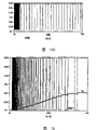
Such a comparator 53 capability is provided when used to dynamically switch the switch matrix 44 as shown below. In short, the flying-spot capacitor C should advantageously be switched only when required by the closed-loop method, and not according to the open-loop oscillator method FLy And (4) switching. The basic idea is to use the output capacitor C as OUT Flying-spot capacitor C when a certain predetermined threshold voltage (V1) is reached FLY A transition to the discharge mode occurs. At this point, the flying spot capacitance C Fly Will be the output capacitor C OUT And (6) charging. When the output capacitor C OUT When a certain voltage (V2) is reached, the flying spot capacitance C Fly Disconnect and return to voltaic cell 36 to be charged. It is critical that switching be based only on these voltages.
FIG. 8 shows the output capacitor C OUT A voltage profile during the time interval required for charging. Assuming that these part parameters are selected as follows: r2=6k Ω; r3=1k Ω; r4= 6k Ω; r5=1k Ω; r6=100k Ω; r7= RS = Rg =10k; r10= R11=25 k Ω; c3=10pF; c4= C5=1pF. Depicted is a voltage diagram of the switching signal SI for switches Q1 and Q3 of switch matrix 44 of fig. 4, which signal SI is generated by first comparator 53 of fig. 7. And is plotted on the output capacitor C OUT The sensed output voltage Vo is returned to the first comparator 53 as the measurement signal M2. It is apparent from fig. 8 that one aspect of the operation of comparator 53 is how the switching rate varies according to the loading of battery 28.
Fig. 9 is a longer period of the voltage graph of fig. 8 to represent steady state operation of power converter 30 to enhance dynamic operation of comparator 53 on load demand.
Fig. 10 is a circuit diagram for switch matrix controller 46 that utilizes a comparator biased by voltage divider 54 to a predetermined threshold.
Fig. 10A is a graph of exemplary voltages at time out of the switch-matrix controller of fig. 10, showing a desired hysteresis in the switch commands of the switch matrix when the output voltage changes around a predetermined threshold value. Assume that the part parameters of FIG. 10 are selected as follows: r22=1M Ω; r23=40 k Ω; r24=10M Ω; r27=1M Ω; r28=200k Ω; c21=22pF.
Fig. 11 is a circuit block diagram for the second comparator 53 of the switch matrix controller 46 of fig. 10. Specifically, differential amplifier 55, differential amplifier 56, decision amplifier 57, hysteresis decision amplifier 58, self-bias amplifier 59, inverter 60, and inverter 61 are depicted as being coupled in series.
Fig. 11A is a first pair of differential amplifiers 55 after a hysteresis decision amplifier 56 for the second comparator 48 of fig. 11.
Fig. 11B is a second pair of differential amplifiers 57 after the hysteresis decision amplifier 58 for the second comparator 48 of fig. 11.
Fig. 11C is a self-biasing amplifier 59 for the second comparator 48 of fig. 11.
Fig. 11D is a pair of inverters 60, 61 for the second comparator 48 of fig. 11.
Fig. 12A-12D show voltage graphs representative of the second comparator 48' shown in fig. 11, 11A-D, and in particular fig. 12A includes a first differential amplifier, hysteretic decision amplifier 65 pair, fig. 12B includes a second differential amplifier 66, hysteretic decision amplifier 67, fig. 12c includes a self-biasing amplifier 68, and fig. 12D includes a pair of inverters 69, 70.
FIG. 13 is a schematic diagram for the output capacitor C OUT Fig. 12B and 12D are voltage charts of the initial charging period of (a).
Fig. 14 is a circuit block diagram of the third comparator 48 for the switch matrix controller 46 of fig. 10. In particular, first and second differential amplifiers 72, 73 with built-in hysteresis, a high gain rail to rail74 and first, second and third inverters 75, 76 and 77.
Fig. 14A is a pair of differential amplifiers with built-in hysteresis 72, 73 for the comparator 48 "of fig. 14.
Fig. 14B is a high gain rail-to-rail (high gain rail-to-rail) schmitt trigger 74a for the comparator 48 "of fig. 14.
Fig. 14C is three inverters 75, 76, 77 for the comparator 48 "of fig. 14 to align the switching points.
Fig. 15A is a graph showing the current sink (drain) along with the switch matrix state shown in fig. 15B for the comparator 48 "of fig. 14, 14A-C.
Fig. 16 is a circuit diagram of a single stage boost chain internal power supply 56A for the Application Specific Integrated Circuit (ASIC) 48 of fig. 2, with fig. 16A depicting a suitable sequence of clock signals for the circuit.
Fig. 17 is a circuit diagram of a multi-stage boost intra-chain power supply 56b for the Application Specific Integrated Circuit (ASIC) 48 of fig. 2, with fig. 17A depicting a suitable sequence of clock signals for the circuit. The multi-stage boost chain internal power supply 56b is formed from a series combination of two single stage boost chain internal power supplies 56a', 56a ".
Fig. 18 is a voltage chart of each stage 56a', 56a "of the multi-stage boost chain internal power supply 56b of fig. 17 over time.
Those skilled in the art will appreciate the benefit of this disclosure, although capacitive switch matrix 44 is shown with one load capacitor C OUT And a flying spot capacitor C FLY But more than two capacitances may be employed in order to obtain the desired capacitance. Additionally, although a capacitive charge pump 26 is shown, multiple stages of charge pumps may be employed to further regulate the voltage potential (Vo) at the terminals 38, 40 of the battery 28. Additionally, the 28 with the built-in dynamic switched capacitor power converter 30 may include one or more voltaic cells 36. Furthermore, while the power converter 30 is illustratively beneficially incorporated into the battery 28, various versions in accordance with aspects of the invention may be separate components and/or employ other types of energy sources 12
Furthermore, although one comparator 53 is shown to provide a closed loop control function that is useful for dynamic switching control, those skilled in the art will recognize that a closed loop scheme that performs some form of comparison may be substituted, with either the voltage threshold being robustly adjusted or not adjusted. This allows, for example, the oscillator open loop control function to be eliminated.
PWM control of an inductor-capacitor power converter
Referring to fig. 19A, a schematic diagram of the top layer of a reverse power output stage 80a for a power converter 82a is depicted, as an example of a buck power converter, providing an output voltage Vo less than an input voltage Vs. The inverting output stage 80a is coupled to the energy source 12 at input terminals 24, 25 and to the load device 14 at output terminals 26, 27 to transfer energy from the energy source 12 to the load device 14. The power supply 12 provides an input voltage Vs and an input current i s . The load device 14 receives a current i O And an output voltage V o 。
The inverting output stage 80a includes a switch MS, a rectifying element MR, an inductive element such as an inductor L, and a capacitive element such as a capacitor C ouT 。C ouT Having its positive terminal 84 coupled to positive output terminal 26, having its negative terminal 86 coupled to negative output terminal 27, and also to negative input terminal 25, which forms a ground reference. Load capacitor C ouT And thus is charged as the output voltage Vo. Inductor L has its positive terminal 88 coupled to a voltage having a feedback voltage V F A node of (2). Feedback voltage V F With the voltage V through the inductor L F It is related. The inductance L has its negative terminal 90 coupled to the positive output terminal 26.
The rectifying element MR, implemented as a MOSFET configured as a synchronous rectifier, has its positive terminal (source) 92 coupled to the feedback voltage node VF and its negative terminal (drain) 94 coupled to the negative input and output terminals 25, 27. The rectifying element MR is turned off in response to the control signal S1. The MOSFET of the rectifying element MR has a channel for reverse conduction current, thereby operating like a diode by reverse comparison of the source and drain with the MOSFET switch MS. Switch MS has its positive terminal (drain) 96 coupled to positive input terminal 24 and its negative terminal (source) 98 coupled to feedback voltage node Vt. The switch MS is closed in response to the on control signal S2.
During the discharge state, the control signal S1 is switched on to turn off the rectifying element MR so that it is on and the control signal S2 is switched off toSwitch MS is turned on, allowing inductor L to discharge to load capacitor C ouT . During the charging state, control signal S1 is off to turn on or render the rectifying element non-conductive MR and control signal S2 is on to turn off switch MS, allowing this inductance to be energized by the input current from power supply 12.
Referring to fig. 19B, a boost power output stage 80B for a power converter 82B illustrates one configuration suitable for boosting the output voltage Vo relative to this input voltage Vs. Load capacitor C ouT Having its positive terminal 84 coupled to the positive output terminal 26, having its negative terminal 86 coupled to the negative output terminal 27, and also to the ground reference 25. Load capacitor C ouT And thus is charged to the output voltage Vo. Inductor L has its negative terminal 90 coupled to a voltage having a feedback voltage V F And has its positive terminal 88 coupled to the positive input terminal 24. An inductor voltage VL is defined between input terminal 24 and feedback voltage node Vs. The inductor voltage VL is thus equal to the feedback voltage V F The input voltage Vs is subtracted.
The rectifying element MR has its negative terminal 94 coupled to the node V L Load capacitor C ouT Also coupled to the positive output 26. The rectifying element MR has its positive terminal 92 coupled to the feedback voltage node Vp. The MOSFET switch MS has its positive terminal (drain) 96 coupled to the feedback voltage node VF and its negative terminal (source) 98 coupled to the negative input and output terminals 25, 27.
During the discharge state, the MOSFET switch MS is turned on in response to the off control signal S2 and the rectifying element MR is turned off in response to the on control signal S1, thereby connecting the power supply 12 and the inductor L to the load capacitor C L . Thus, the input voltage VL and the inductor voltage VL are added to increase the capacitance C given to the lead L And output voltage Vo. During the charging state, the MOSFET switch MS is turned off in response to the turn-on control signal S2, thereby coupling the inductor L through the power supply 12. The rectifying element MR is turned on in response to the turn-off control signal S1 to turn off the load capacitor C ouT With the power supply 12 and the inductor L.
In accordance with one aspect of the present invention, both the reverse power output stage 80a of fig. 19A and the boost power output stage 80B of fig. 19B are advantageously efficient and operable at low input voltages (e.g., less than one volt), to be realized by (two metal, two poly-salicide) integrated circuit devices fabricated in a 0.35 micron dual-salicide process using MOSFET transistor switches capable of low threshold (e.g., less than one volt), as described in the pending and commonly owned applications, all filed on march 22 of 2000 by Ying Xu et al, U.S. serial No. 09/532,761, entitled "Asymmetric Lightly Doped depletion MOSFET '(a" Asymmetric Lightly Doped MOSFET'). (P G case No. 7992), incorporated herein by reference. Unlike having a low threshold control, the disclosed MOSFET device has a low pass conduction resistance, directly improving the efficiency of the power output stages 80a and 80b used in the present invention.
Referring to fig. 20, start-stop power converter 82b switchably controls power output 80b of graph 1913 using start-stop controller 100. Known power converters, including inductive power converters, do not oscillate continuously even when the load device 14 demand is low, making the power converter oscillate inefficiently. Therefore, start-stop controller 100 advantageously stops the oscillation of the Pulse Width Modulation (PWM) output when lead capacitor Cout is sufficiently charged.
Specifically, boost power output stage 80B is illustrated in fig. 19B, with the addition of capacitor C1 in addition to the additional C1 coupled through input terminal 24 to enhance the stability of input voltage Vs.
Start-stop controller 100 responds to a Pulse Width Modulation (PWM) input signal by selectively generating a control signal S1 by turning off rectifying element MR during a discharge state and turning on rectifying element MR during a charge state, and selectively generating a control signal S2 by turning on switch MS during a discharge state and turning off MS during a charge state. Start-stop controller 100 senses a reference voltage V from voltage reference 104 REF Low demand for delayed stopping as shown by comparison with the output voltage VoThe ringing control signal causes the output stage 80b to remain in the discharge state. Start-stop controller 100 includes a hysteretic comparator 106 responsive to a reference voltage V REF Output voltage Vo and feedback voltage V F To generate a duty cycle signal and lags the response output voltage Vo against the reference voltage VREF to generate a stop signal. The modulator 108 generates an oscillating signal having a predetermined frequency from a fixed frequency oscillator 110. The SR flip-flop 112 is set by the set cyclic operation signal and reset by the signal to generate a switching signal that determines the charge state and the discharge state. The multiplexer 114 is responsive to the switching signal to generate the control signals S1 and S2. Multiplexer 114 has a predetermined state switching delay to regulate cross conduction of power output stage 80 h. The multiplexer 114 also responds to the stop signal by turning off the control signal S2 to turn on the switch MS and by turning off the rectifying element MIL by turning on the control signal SI to stop the oscillation until more energy is needed.
In addition, the start-up circuit 116 biases the start-stop controller 100 when discharging at the power output stage 80b, and provides a start charge for the CL.
Referring to fig. 21, the operation of start-stop power converter 82a is illustrated in a timing diagram. In many applicationsThe source voltage Vs in the power source 14, such as one composed of electrochemical voltaic cells, tends to decay over time, eventually below the nominal voltage V of the power source class 12 NoM 。
The output voltage Vo is initially below two voltage thresholds V OFF And Vo. The duty cycle of the switch between charging and discharging is a predetermined value, which is responsive to a drop in the source voltage to maintain the output voltage Vo, taking into account the capacitance and inductance values of the element and the desired output voltage Fo. The operation of the switching cycle continues until the output voltage Vo is greater than the voltage threshold Vow, so that the hysteresis comparator 70 sends a signal to the multiplexer 114 to stop outputting the switching signals S1 and S2, thereby turning on the rectifying element MR and the switch MS. The load device 14 draws stored energy from the output capacitor Cout, dropping the output voltage Ilo Ilo until it drops below the voltage gateLimit of V oFF . However, when the output voltage Vo is lowered to the voltage threshold V ON In the following, comparator 70 lags behind time B in response to restart switching signals S1 and S2 before sending the signals to multiplexer 114.
The invention in its broader aspects is not limited to the specific details, representative and method, and illustrative examples shown and described. Accordingly, departures may be made from such details without departing from the spirit or scope of the applicant's general inventive concept.
Claims (8)
1. A battery, comprising:
a voltaic cell comprising positive and negative electrodes, the cell storing an electrical charge resulting in an electrode voltage across the positive and negative electrodes;
a housing substantially enclosing the voltaic cell, the housing including a positive terminal and a negative terminal; characterized in that the battery further comprises:
a dynamically switched capacitive charge pump electrically interposed between the electrodes and the terminals, the charge pump substantially surrounded by a housing, and wherein said dynamically switched capacitive charge pump comprises a load capacitor electrically coupled across said terminals, a flying spot capacitor, and an integrated circuit comprising:
a switch matrix electrically switched between a charging mode and a discharging mode, wherein the switch matrix in the charging mode comprises a switch configured to charge the flying spot capacitor by electrically coupling the flying spot capacitor in series with the voltaic cell, and wherein the switch matrix in the discharging mode comprises a switch configured to discharge the flying spot capacitor by electrically coupling the flying spot capacitor in series with the load capacitor; and
a switch matrix controller is operably coupled to the switch matrix to select the charging and discharging modes, but only needs to maintain the output voltage at a desired value.
2. The battery of claim 1, wherein the switch matrix controller includes a comparator responsive to the output voltage falling below a predetermined threshold value to command the switch matrix to the discharge mode and responsive to the output voltage being above the predetermined threshold value to command the switch matrix to the charge mode, and wherein the comparator includes hysteresis circuitry to prevent rapid oscillation when the output voltage approaches the predetermined threshold value, or the comparator includes an output stage including an amplifier and hysteresis device.
3. The battery of claim 1, further comprising:
an internal power source electrically coupled to the voltaic cell voltage power source, the internal power source electrically biasing the switch matrix controller; and
a voltage reference circuit providing a voltage reference to the switch matrix controller, said voltage reference circuit comprising a temperature compensation circuit for the voltage reference circuit.
4. The battery of claim 1, wherein the switch matrix comprises a first switch electrically switchably coupling the positive electrode to a first terminal of the flying-spot capacitor; a second switch electrically switchably coupling a first end of the flying-spot capacitor to a positive terminal of the battery; a third switch electrically coupled to the cathode to the second terminal of the flying spot capacitor; and a fourth switch electrically coupling the second terminal of the flying-spot capacitor to the positive electrode, wherein the first switch, the second switch, the third switch, and the fourth switch are each comprised of a field effect integrated circuit, wherein the first and third switches are closed and the second and fourth switches are open to affect the charge mode and vice versa to affect the discharge mode.
5. The cell of claim 1, wherein the voltaic cell comprises a selected one of a lithium-ion electrochemical cell and an alkaline electrochemical cell.
6. The battery of claim 1, wherein the flying-spot capacitor comprises a high-efficiency capacitor.
7. A power management circuit configured to regulate the output voltage of positive and negative terminals of a battery, the battery further comprising a voltaic cell having positive and negative electrodes, an energy storage device, and a load capacitor electrically coupled across the terminals, the power management circuit comprising:
a switch matrix electrically switchable between a charging mode and a discharging mode, wherein the switch matrix, in the charging mode, includes being configured to charge the energy storage device by electrically coupling the energy storage device in series with the voltaic cell, and wherein the switch matrix, in the discharging mode, includes being configured to discharge the energy storage device by electrically coupling the energy storage device in series with the load capacitor; and
a switch matrix controller operatively coupled to the switch matrix to select the charge-discharge mode, but only needs to maintain the output voltage at a desired value.
8. The power management circuit of claim 7, wherein the switch matrix comprises one of:
a non-inverting switched capacitor device, and an inverting switched capacitor device.
Applications Claiming Priority (2)
| Application Number | Priority Date | Filing Date | Title |
|---|---|---|---|
| US14111999P | 1999-06-25 | 1999-06-25 | |
| US60/141,119 | 1999-06-25 |
Publications (2)
| Publication Number | Publication Date |
|---|---|
| CN1371543A CN1371543A (en) | 2002-09-25 |
| CN100364222C true CN100364222C (en) | 2008-01-23 |
Family
ID=22494240
Family Applications (1)
| Application Number | Title | Priority Date | Filing Date |
|---|---|---|---|
| CNB008120293A Expired - Fee Related CN100364222C (en) | 1999-06-25 | 2000-06-23 | Dynamically-switched power converter |
Country Status (12)
| Country | Link |
|---|---|
| US (2) | US6646415B1 (en) |
| EP (1) | EP1190480B1 (en) |
| JP (2) | JP3820149B2 (en) |
| KR (1) | KR100462094B1 (en) |
| CN (1) | CN100364222C (en) |
| AT (1) | ATE282904T1 (en) |
| AU (1) | AU5884500A (en) |
| CA (1) | CA2377166C (en) |
| DE (1) | DE60015972T2 (en) |
| IL (1) | IL147067A0 (en) |
| MX (1) | MXPA01013024A (en) |
| WO (1) | WO2001001553A1 (en) |
Cited By (2)
| Publication number | Priority date | Publication date | Assignee | Title |
|---|---|---|---|---|
| CN101741403B (en) * | 2008-11-10 | 2013-08-21 | 索尼移动通信日本株式会社 | Wireless communication apparatus and power-supply apparatus |
| CN108116350A (en) * | 2018-01-08 | 2018-06-05 | 卢浩义 | Vehicle-mounted assembled battery intelligent power supply electric system and method for supplying power to |
Families Citing this family (118)
| Publication number | Priority date | Publication date | Assignee | Title |
|---|---|---|---|---|
| US6724220B1 (en) | 2000-10-26 | 2004-04-20 | Cyress Semiconductor Corporation | Programmable microcontroller architecture (mixed analog/digital) |
| US6892310B1 (en) * | 2000-10-26 | 2005-05-10 | Cypress Semiconductor Corporation | Method for efficient supply of power to a microcontroller |
| US8103496B1 (en) | 2000-10-26 | 2012-01-24 | Cypress Semicondutor Corporation | Breakpoint control in an in-circuit emulation system |
| US8160864B1 (en) | 2000-10-26 | 2012-04-17 | Cypress Semiconductor Corporation | In-circuit emulator and pod synchronized boot |
| US8149048B1 (en) | 2000-10-26 | 2012-04-03 | Cypress Semiconductor Corporation | Apparatus and method for programmable power management in a programmable analog circuit block |
| US8176296B2 (en) | 2000-10-26 | 2012-05-08 | Cypress Semiconductor Corporation | Programmable microcontroller architecture |
| US7765095B1 (en) | 2000-10-26 | 2010-07-27 | Cypress Semiconductor Corporation | Conditional branching in an in-circuit emulation system |
| FR2828029B1 (en) * | 2001-07-25 | 2003-09-26 | Centre Nat Rech Scient | ENERGY CONVERSION DEVICE |
| US7406674B1 (en) | 2001-10-24 | 2008-07-29 | Cypress Semiconductor Corporation | Method and apparatus for generating microcontroller configuration information |
| US8078970B1 (en) | 2001-11-09 | 2011-12-13 | Cypress Semiconductor Corporation | Graphical user interface with user-selectable list-box |
| US8042093B1 (en) | 2001-11-15 | 2011-10-18 | Cypress Semiconductor Corporation | System providing automatic source code generation for personalization and parameterization of user modules |
| US7774190B1 (en) | 2001-11-19 | 2010-08-10 | Cypress Semiconductor Corporation | Sleep and stall in an in-circuit emulation system |
| US7844437B1 (en) | 2001-11-19 | 2010-11-30 | Cypress Semiconductor Corporation | System and method for performing next placements and pruning of disallowed placements for programming an integrated circuit |
| US8069405B1 (en) | 2001-11-19 | 2011-11-29 | Cypress Semiconductor Corporation | User interface for efficiently browsing an electronic document using data-driven tabs |
| US7770113B1 (en) | 2001-11-19 | 2010-08-03 | Cypress Semiconductor Corporation | System and method for dynamically generating a configuration datasheet |
| US6971004B1 (en) | 2001-11-19 | 2005-11-29 | Cypress Semiconductor Corp. | System and method of dynamically reconfiguring a programmable integrated circuit |
| US8103497B1 (en) | 2002-03-28 | 2012-01-24 | Cypress Semiconductor Corporation | External interface for event architecture |
| KR100485032B1 (en) * | 2002-04-09 | 2005-04-22 | 김선호 | The method for manufacturing of natural dyes |
| US7308608B1 (en) | 2002-05-01 | 2007-12-11 | Cypress Semiconductor Corporation | Reconfigurable testing system and method |
| US6864669B1 (en) * | 2002-05-02 | 2005-03-08 | O2Micro International Limited | Power supply block with simplified switch configuration |
| US7761845B1 (en) | 2002-09-09 | 2010-07-20 | Cypress Semiconductor Corporation | Method for parameterizing a user module |
| ITMI20022268A1 (en) * | 2002-10-25 | 2004-04-26 | Atmel Corp | VARIABLE CHARGE PUMP CIRCUIT WITH DYNAMIC LOAD |
| US6888339B1 (en) * | 2003-04-03 | 2005-05-03 | Lockheed Martin Corporation | Bus voltage control using gated fixed energy pulses |
| CN100423421C (en) * | 2003-05-13 | 2008-10-01 | 富士通株式会社 | Semiconductor integrated circuit device |
| ES2537655T3 (en) | 2003-09-18 | 2015-06-10 | Commonwealth Scientific And Industrial Research Organisation | High performance energy storage devices |
| JP4547387B2 (en) * | 2003-12-17 | 2010-09-22 | コーニンクレッカ フィリップス エレクトロニクス エヌ ヴィ | Emergency light device and emergency light system |
| US7190210B2 (en) * | 2004-03-25 | 2007-03-13 | Integral Wave Technologies, Inc. | Switched-capacitor power supply system and method |
| US7295049B1 (en) | 2004-03-25 | 2007-11-13 | Cypress Semiconductor Corporation | Method and circuit for rapid alignment of signals |
| US7239194B2 (en) * | 2004-03-25 | 2007-07-03 | Integral Wave Technologies, Inc. | Trench capacitor power supply system and method |
| US8069436B2 (en) | 2004-08-13 | 2011-11-29 | Cypress Semiconductor Corporation | Providing hardware independence to automate code generation of processing device firmware |
| US8286125B2 (en) | 2004-08-13 | 2012-10-09 | Cypress Semiconductor Corporation | Model for a hardware device-independent method of defining embedded firmware for programmable systems |
| US7332976B1 (en) | 2005-02-04 | 2008-02-19 | Cypress Semiconductor Corporation | Poly-phase frequency synthesis oscillator |
| US7372277B2 (en) * | 2005-04-15 | 2008-05-13 | Agamatrix, Inc. | Method and apparatus for providing stable voltage to analytical system |
| US7400183B1 (en) | 2005-05-05 | 2008-07-15 | Cypress Semiconductor Corporation | Voltage controlled oscillator delay cell and method |
| US8089461B2 (en) | 2005-06-23 | 2012-01-03 | Cypress Semiconductor Corporation | Touch wake for electronic devices |
| US8184430B2 (en) * | 2005-06-29 | 2012-05-22 | Harman International Industries, Incorporated | Vehicle media system |
| JP4177364B2 (en) * | 2005-09-12 | 2008-11-05 | 三菱電機株式会社 | Constant voltage controller |
| US7417416B2 (en) * | 2005-10-27 | 2008-08-26 | International Business Machines Corporation | Regulator with load tracking bias |
| US8085067B1 (en) | 2005-12-21 | 2011-12-27 | Cypress Semiconductor Corporation | Differential-to-single ended signal converter circuit and method |
| US7692411B2 (en) | 2006-01-05 | 2010-04-06 | Tpl, Inc. | System for energy harvesting and/or generation, storage, and delivery |
| US8004213B2 (en) * | 2006-02-17 | 2011-08-23 | Rohm Co., Ltd. | Power supply, light emission control device and display device |
| US8067948B2 (en) | 2006-03-27 | 2011-11-29 | Cypress Semiconductor Corporation | Input/output multiplexer bus |
| US7365585B2 (en) * | 2006-08-09 | 2008-04-29 | Atmel Corporation | Apparatus and method for charge pump slew rate control |
| JP4826383B2 (en) * | 2006-08-10 | 2011-11-30 | セイコーエプソン株式会社 | Power supply circuit, display driver, electro-optical device, and electronic device |
| DE102006040186B4 (en) * | 2006-08-26 | 2008-07-31 | Robert Bosch Gmbh | Method for operating an electrical device |
| US7864507B2 (en) | 2006-09-06 | 2011-01-04 | Tpl, Inc. | Capacitors with low equivalent series resistance |
| US7764526B1 (en) * | 2006-10-18 | 2010-07-27 | Intersil Americas Inc. | Hysteretic mode controller for capacitor voltage divider |
| AR064292A1 (en) | 2006-12-12 | 2009-03-25 | Commw Scient Ind Res Org | ENHANCED ENERGY STORAGE DEVICE |
| GB2447426B (en) * | 2006-12-22 | 2011-07-13 | Wolfson Microelectronics Plc | Charge pump circuit and methods of operation thereof |
| GB2444984B (en) * | 2006-12-22 | 2011-07-13 | Wolfson Microelectronics Plc | Charge pump circuit and methods of operation thereof |
| AR067238A1 (en) | 2007-03-20 | 2009-10-07 | Commw Scient Ind Res Org | OPTIMIZED DEVICES FOR ENERGY STORAGE |
| US9564902B2 (en) | 2007-04-17 | 2017-02-07 | Cypress Semiconductor Corporation | Dynamically configurable and re-configurable data path |
| US8092083B2 (en) | 2007-04-17 | 2012-01-10 | Cypress Semiconductor Corporation | Temperature sensor with digital bandgap |
| US8040266B2 (en) | 2007-04-17 | 2011-10-18 | Cypress Semiconductor Corporation | Programmable sigma-delta analog-to-digital converter |
| US7737724B2 (en) | 2007-04-17 | 2010-06-15 | Cypress Semiconductor Corporation | Universal digital block interconnection and channel routing |
| US8026739B2 (en) | 2007-04-17 | 2011-09-27 | Cypress Semiconductor Corporation | System level interconnect with programmable switching |
| US8130025B2 (en) | 2007-04-17 | 2012-03-06 | Cypress Semiconductor Corporation | Numerical band gap |
| US8516025B2 (en) | 2007-04-17 | 2013-08-20 | Cypress Semiconductor Corporation | Clock driven dynamic datapath chaining |
| US9720805B1 (en) | 2007-04-25 | 2017-08-01 | Cypress Semiconductor Corporation | System and method for controlling a target device |
| US8065653B1 (en) | 2007-04-25 | 2011-11-22 | Cypress Semiconductor Corporation | Configuration of programmable IC design elements |
| US8266575B1 (en) | 2007-04-25 | 2012-09-11 | Cypress Semiconductor Corporation | Systems and methods for dynamically reconfiguring a programmable system on a chip |
| TW200847599A (en) * | 2007-05-29 | 2008-12-01 | Novatek Microelectronics Corp | Voltage regulator and voltage regulating method thereof and voltage producer with voltage regulator disclosed by the present invention |
| JP5222628B2 (en) * | 2007-05-31 | 2013-06-26 | 株式会社半導体エネルギー研究所 | Semiconductor device |
| WO2008152548A1 (en) * | 2007-06-14 | 2008-12-18 | Nxp B.V. | Switched-mode dc-dc converter and an integrated system comprising such a converter |
| US8049569B1 (en) | 2007-09-05 | 2011-11-01 | Cypress Semiconductor Corporation | Circuit and method for improving the accuracy of a crystal-less oscillator having dual-frequency modes |
| KR100933585B1 (en) * | 2007-11-26 | 2009-12-23 | 연세대학교 산학협력단 | Tracking Analog-to-Digital Converter with Hysteresis |
| KR100917976B1 (en) * | 2007-12-13 | 2009-09-18 | 주식회사 에이디텍 | Power supply for multiple output voltages |
| US8432070B2 (en) * | 2008-08-25 | 2013-04-30 | Qualcomm Incorporated | Passive receivers for wireless power transmission |
| US8947041B2 (en) * | 2008-09-02 | 2015-02-03 | Qualcomm Incorporated | Bidirectional wireless power transmission |
| US8532724B2 (en) | 2008-09-17 | 2013-09-10 | Qualcomm Incorporated | Transmitters for wireless power transmission |
| CN102484245B (en) | 2009-04-23 | 2015-11-25 | 古河电池株式会社 | The manufacture method of negative electrode plate for lead storage battery and lead accumulator |
| US9448964B2 (en) | 2009-05-04 | 2016-09-20 | Cypress Semiconductor Corporation | Autonomous control in a programmable system |
| FR2945876B1 (en) * | 2009-05-19 | 2012-03-23 | St Microelectronics Sa | DEVICE FOR CONTROLLING A LOAD PUMP GENERATOR AND CORRESPONDING REGULATION METHOD |
| JP4840481B2 (en) * | 2009-07-08 | 2011-12-21 | トヨタ自動車株式会社 | Secondary battery temperature increase control device, vehicle equipped with the same, and secondary battery temperature increase control method |
| JP5797384B2 (en) | 2009-08-27 | 2015-10-21 | 古河電池株式会社 | Composite capacitor negative electrode plate for lead acid battery and lead acid battery |
| MX2012002415A (en) | 2009-08-27 | 2012-06-25 | Commw Scient Ind Res Org | Electrical storage device and electrode thereof. |
| JP5711483B2 (en) | 2009-08-27 | 2015-04-30 | 古河電池株式会社 | Method for producing negative electrode plate of composite capacitor for lead storage battery and lead storage battery |
| TWI400592B (en) * | 2009-09-15 | 2013-07-01 | Acer Inc | Low dropout regulator |
| US8598737B2 (en) | 2010-12-13 | 2013-12-03 | Light-Based Technologies Incorporated | Synchronous switching power supply |
| JP2012133959A (en) | 2010-12-21 | 2012-07-12 | Furukawa Battery Co Ltd:The | Composite capacitor negative electrode plate for lead storage battery, and lead storage battery |
| US9450412B2 (en) * | 2010-12-22 | 2016-09-20 | General Electric Company | Method and system for control power in remote DC power systems |
| CN103582997B (en) | 2011-02-24 | 2017-02-15 | 克兰电子公司 | AC/DC power conversion system and method of manufacture of same |
| US8791679B2 (en) * | 2011-03-31 | 2014-07-29 | Fairchild Semiconductor Corporation | Self-sustaining, high voltage tolerant power supply |
| CN102262193B (en) * | 2011-06-13 | 2013-08-21 | 深圳市普联技术有限公司 | Circuit and method for testing capacitive load |
| US8885308B2 (en) | 2011-07-18 | 2014-11-11 | Crane Electronics, Inc. | Input control apparatus and method with inrush current, under and over voltage handling |
| US8824167B2 (en) * | 2011-07-18 | 2014-09-02 | Crane Electronics, Inc. | Self synchronizing power converter apparatus and method suitable for auxiliary bias for dynamic load applications |
| US8890630B2 (en) | 2011-07-18 | 2014-11-18 | Crane Electronics, Inc. | Oscillator apparatus and method with wide adjustable frequency range |
| US8866551B2 (en) | 2012-09-10 | 2014-10-21 | Crane Electronics, Inc. | Impedance compensation for operational amplifiers used in variable environments |
| KR101419645B1 (en) * | 2013-02-19 | 2014-07-17 | 중앙대학교 산학협력단 | Dc-dc converter with multi-output using switched capacitor |
| US9002447B2 (en) | 2013-03-14 | 2015-04-07 | Medtronic, Inc. | Implantable medical device having power supply for generating a regulated power supply |
| US20150008867A1 (en) * | 2013-07-03 | 2015-01-08 | At&T Intellectual Property I, L.P. | Charge pump battery charging |
| US9484807B2 (en) * | 2013-07-26 | 2016-11-01 | Maxlinear, Inc. | High efficiency switched capacitor voltage regulator |
| US9603205B2 (en) * | 2014-07-07 | 2017-03-21 | Dialog Semiconductor Inc. | Multi-function terminal configurable to implement two functionalities |
| US9041378B1 (en) | 2014-07-17 | 2015-05-26 | Crane Electronics, Inc. | Dynamic maneuvering configuration for multiple control modes in a unified servo system |
| US9831768B2 (en) | 2014-07-17 | 2017-11-28 | Crane Electronics, Inc. | Dynamic maneuvering configuration for multiple control modes in a unified servo system |
| US9230726B1 (en) | 2015-02-20 | 2016-01-05 | Crane Electronics, Inc. | Transformer-based power converters with 3D printed microchannel heat sink |
| US9160228B1 (en) | 2015-02-26 | 2015-10-13 | Crane Electronics, Inc. | Integrated tri-state electromagnetic interference filter and line conditioning module |
| KR102381085B1 (en) | 2015-02-27 | 2022-04-01 | 삼성전자주식회사 | Dc-dc converter, charging integrated circuit and electronic device having the same and battery charging method thereof |
| US9293999B1 (en) | 2015-07-17 | 2016-03-22 | Crane Electronics, Inc. | Automatic enhanced self-driven synchronous rectification for power converters |
| KR102562313B1 (en) * | 2016-02-19 | 2023-08-01 | 삼성전자주식회사 | Display driver ic and display system having the same |
| US9780635B1 (en) | 2016-06-10 | 2017-10-03 | Crane Electronics, Inc. | Dynamic sharing average current mode control for active-reset and self-driven synchronous rectification for power converters |
| US10447158B2 (en) | 2016-07-01 | 2019-10-15 | Texas Instruments Incorporated | Reducing voltage rating of devices in a multilevel converter |
| EP3526888A4 (en) | 2016-10-11 | 2020-04-01 | Commscope Technologies LLC | Systems and methods for high efficiency power conversion |
| US9735566B1 (en) | 2016-12-12 | 2017-08-15 | Crane Electronics, Inc. | Proactively operational over-voltage protection circuit |
| US9742183B1 (en) | 2016-12-09 | 2017-08-22 | Crane Electronics, Inc. | Proactively operational over-voltage protection circuit |
| EP3593437B1 (en) * | 2017-03-07 | 2022-11-02 | Volt Technology Limited | Battery with a voltage regulation device |
| WO2018227278A1 (en) * | 2017-06-12 | 2018-12-20 | Gbatteries Energy Canada Inc. | Battery charging through multi-stage voltage conversion |
| US9979285B1 (en) | 2017-10-17 | 2018-05-22 | Crane Electronics, Inc. | Radiation tolerant, analog latch peak current mode control for power converters |
| US10389236B1 (en) * | 2018-03-29 | 2019-08-20 | Psemi Corporation | Disturbance quelling |
| US10425080B1 (en) | 2018-11-06 | 2019-09-24 | Crane Electronics, Inc. | Magnetic peak current mode control for radiation tolerant active driven synchronous power converters |
| US10671111B1 (en) | 2018-12-18 | 2020-06-02 | Analog Devices International Unlimited Company | Supply voltage apparatus with integrated gain adjustment and multiple supply monitoring |
| CN109379070A (en) * | 2018-12-20 | 2019-02-22 | 上海艾为电子技术股份有限公司 | A kind of analog switch start-up circuit and method |
| US11791650B2 (en) * | 2019-03-18 | 2023-10-17 | Texas Instruments Incorporated | Multiple output charging system and controller |
| US11848581B2 (en) * | 2019-06-14 | 2023-12-19 | X-wave Innovations, Inc. | Source bootstrap power conversion for the safe and efficient interconnection of homogeneous or heterogeneous energy storage modules |
| CN112332828A (en) * | 2020-09-15 | 2021-02-05 | 南京芯思科技有限公司 | Charging circuit, analog receiving circuit and charging method based on self-capacitance touch screen |
| EP4096078A1 (en) * | 2021-05-28 | 2022-11-30 | Oticon A/s | Hearing device having a power source |
| CN116231590A (en) | 2021-12-02 | 2023-06-06 | 财团法人工业技术研究院 | Power supply |
| US20230208295A1 (en) * | 2021-12-28 | 2023-06-29 | Novatek Microelectronics Corp. | Power supply circuit for switching converter |
Citations (3)
| Publication number | Priority date | Publication date | Assignee | Title |
|---|---|---|---|---|
| DE3608082A1 (en) * | 1986-03-07 | 1987-09-10 | Licentia Gmbh | Circuit arrangement for stabilising the output DC voltage with a varying input DC voltage of a step-down/step-up controller combination |
| EP0653798A1 (en) * | 1993-11-05 | 1995-05-17 | Philips Patentverwaltung GmbH | Battery with incorporated voltage converter |
| DE29605699U1 (en) * | 1996-03-27 | 1996-08-01 | Siemens Ag | Battery power supply |
Family Cites Families (46)
| Publication number | Priority date | Publication date | Assignee | Title |
|---|---|---|---|---|
| DE2052382A1 (en) | 1970-10-26 | 1972-04-27 | Meggl F | Process for the transmission of electrical energy between two electrically isolated circuits |
| US3896320A (en) | 1971-10-19 | 1975-07-22 | United Aircraft Corp | High speed electric generator |
| US3811648A (en) | 1973-07-09 | 1974-05-21 | Us Navy | Azimuth readout system |
| GB1597870A (en) | 1977-06-03 | 1981-09-16 | Inoue Japax Res | Electrical machining power supply apparatus |
| SU892424A2 (en) | 1978-04-27 | 1981-12-23 | Предприятие П/Я Г-4934 | Reference voltage source |
| US4617652A (en) * | 1979-01-24 | 1986-10-14 | Xicor, Inc. | Integrated high voltage distribution and control systems |
| EP0057009B1 (en) | 1981-01-28 | 1985-07-03 | Hitachi, Ltd. | Current supply circuit |
| JPS62147954A (en) * | 1985-12-23 | 1987-07-01 | Casio Comput Co Ltd | Step-up circuit |
| US4870341A (en) | 1986-11-26 | 1989-09-26 | First Medical Devices Corporation | Impedance measurement circuit |
| US4785812A (en) | 1986-11-26 | 1988-11-22 | First Medical Devices Corporation | Protection system for preventing defibrillation with incorrect or improperly connected electrodes |
| EP0313914B1 (en) | 1987-10-26 | 1993-03-03 | Siemens Aktiengesellschaft | Circuit comprising an input amplifier connected to an opto-electrical transducer |
| US4814685A (en) * | 1987-12-04 | 1989-03-21 | Pacesetter Infusion, Ltd. | Inductive power converter for use with variable input and output voltages |
| GB9115811D0 (en) | 1991-07-22 | 1991-09-04 | Fujisawa Pharmaceutical Co | Fr901451 substance,process for preparation thereof and use thereof |
| US5392205A (en) | 1991-11-07 | 1995-02-21 | Motorola, Inc. | Regulated charge pump and method therefor |
| CN1075690C (en) | 1991-11-07 | 2001-11-28 | 摩托罗拉公司 | Mixed signal processing system and method for powering same |
| JPH05137320A (en) * | 1991-11-15 | 1993-06-01 | Fuji Electric Co Ltd | Voltage generation circuit |
| US5202594A (en) | 1992-02-04 | 1993-04-13 | Motorola, Inc. | Low power level converter |
| US5591209A (en) | 1994-05-19 | 1997-01-07 | Angeion Corporation | Implantable defibrillator system for generating an active biphasic waveform |
| US5434498A (en) | 1992-12-14 | 1995-07-18 | United Memories, Inc. | Fuse programmable voltage converter with a secondary tuning path |
| US5483152A (en) | 1993-01-12 | 1996-01-09 | United Memories, Inc. | Wide range power supply for integrated circuits |
| US5347172A (en) | 1992-10-22 | 1994-09-13 | United Memories, Inc. | Oscillatorless substrate bias generator |
| US5337284A (en) | 1993-01-11 | 1994-08-09 | United Memories, Inc. | High voltage generator having a self-timed clock circuit and charge pump, and a method therefor |
| US5345376A (en) | 1993-02-19 | 1994-09-06 | Tescom Corporation | Switching power supply with electronic isolation |
| CH688066A5 (en) * | 1994-03-04 | 1997-04-30 | Ascom Frako Gmbh Stromversorgu | AC=DC converter using book- /boost-principle |
| US5532915A (en) | 1994-03-23 | 1996-07-02 | Intel Corporation | Method and apparatus for providing an ultra low power regulated negative charge pump |
| US5622789A (en) * | 1994-09-12 | 1997-04-22 | Apple Computer, Inc. | Battery cell having an internal circuit for controlling its operation |
| DE4442466C1 (en) | 1994-11-29 | 1995-12-14 | Siemens Ag | Circuit for generating regulated output voltage from unregulated input voltage |
| US5479089A (en) * | 1994-12-21 | 1995-12-26 | Hughes Aircraft Company | Power converter apparatus having instantaneous commutation switching system |
| US5889428A (en) | 1995-06-06 | 1999-03-30 | Ramtron International Corporation | Low loss, regulated charge pump with integrated ferroelectric capacitors |
| US5694308A (en) | 1995-07-03 | 1997-12-02 | Motorola, Inc. | Method and apparatus for regulated low voltage charge pump |
| JP2800741B2 (en) * | 1995-09-29 | 1998-09-21 | 日本電気株式会社 | Power circuit |
| US5596532A (en) | 1995-10-18 | 1997-01-21 | Sandisk Corporation | Flash EEPROM self-adaptive voltage generation circuit operative within a continuous voltage source range |
| US5680300A (en) | 1995-12-22 | 1997-10-21 | Analog Devices, Inc. | Regulated charge pump DC/DC converter |
| US5684683A (en) | 1996-02-09 | 1997-11-04 | Wisconsin Alumni Research Foundation | DC-to-DC power conversion with high current output |
| US5627739A (en) | 1996-04-02 | 1997-05-06 | Winbond Electronics Corp. | Regulated charge pump with low noise on the well of the substrate |
| JP3224744B2 (en) | 1996-07-08 | 2001-11-05 | 富士通株式会社 | Step-down DC-DC regulator |
| US5815356A (en) | 1996-09-26 | 1998-09-29 | Power Micro, Inc. | Integrated transient suppressor |
| JPH10290563A (en) * | 1997-02-12 | 1998-10-27 | Mitsubishi Electric Corp | Voltage generating circuit for semiconductor device |
| US5773955A (en) * | 1997-03-11 | 1998-06-30 | Northrop Grumman Corporation | Battery charger apparatus |
| DE19725440A1 (en) * | 1997-06-16 | 1998-12-24 | Siemens Ag | DC/DC converter |
| JP3180898B2 (en) * | 1997-11-14 | 2001-06-25 | 日本電気株式会社 | Boost circuit |
| US6412207B1 (en) * | 1998-06-24 | 2002-07-02 | Caleb Clark Crye | Firearm safety and control system |
| WO2000057567A1 (en) * | 1999-03-23 | 2000-09-28 | Siemens Aktiengesellschaft | Synchronous load doubler-charge pump with an integrated in-phase regulator |
| US6310789B1 (en) * | 1999-06-25 | 2001-10-30 | The Procter & Gamble Company | Dynamically-controlled, intrinsically regulated charge pump power converter |
| TW533667B (en) | 2000-08-31 | 2003-05-21 | Univ Illinois | Multiple output dynamically regulated charge pump power converter |
| US6466070B1 (en) * | 2000-12-21 | 2002-10-15 | Xilinx, Inc. | Low voltage charge pump |
-
2000
- 2000-06-23 DE DE60015972T patent/DE60015972T2/en not_active Expired - Fee Related
- 2000-06-23 CN CNB008120293A patent/CN100364222C/en not_active Expired - Fee Related
- 2000-06-23 IL IL14706700A patent/IL147067A0/en unknown
- 2000-06-23 AT AT00944805T patent/ATE282904T1/en not_active IP Right Cessation
- 2000-06-23 CA CA002377166A patent/CA2377166C/en not_active Expired - Fee Related
- 2000-06-23 EP EP00944805A patent/EP1190480B1/en not_active Expired - Lifetime
- 2000-06-23 US US10/009,872 patent/US6646415B1/en not_active Expired - Fee Related
- 2000-06-23 WO PCT/US2000/017272 patent/WO2001001553A1/en active IP Right Grant
- 2000-06-23 MX MXPA01013024A patent/MXPA01013024A/en unknown
- 2000-06-23 JP JP2001506668A patent/JP3820149B2/en not_active Expired - Fee Related
- 2000-06-23 AU AU58845/00A patent/AU5884500A/en not_active Abandoned
-
2001
- 2001-10-09 US US09/652,849 patent/US6643151B1/en not_active Expired - Fee Related
- 2001-12-26 KR KR10-2001-7016626A patent/KR100462094B1/en not_active IP Right Cessation
-
2006
- 2006-05-18 JP JP2006138703A patent/JP4676377B2/en not_active Expired - Fee Related
Patent Citations (3)
| Publication number | Priority date | Publication date | Assignee | Title |
|---|---|---|---|---|
| DE3608082A1 (en) * | 1986-03-07 | 1987-09-10 | Licentia Gmbh | Circuit arrangement for stabilising the output DC voltage with a varying input DC voltage of a step-down/step-up controller combination |
| EP0653798A1 (en) * | 1993-11-05 | 1995-05-17 | Philips Patentverwaltung GmbH | Battery with incorporated voltage converter |
| DE29605699U1 (en) * | 1996-03-27 | 1996-08-01 | Siemens Ag | Battery power supply |
Cited By (3)
| Publication number | Priority date | Publication date | Assignee | Title |
|---|---|---|---|---|
| CN101741403B (en) * | 2008-11-10 | 2013-08-21 | 索尼移动通信日本株式会社 | Wireless communication apparatus and power-supply apparatus |
| CN108116350A (en) * | 2018-01-08 | 2018-06-05 | 卢浩义 | Vehicle-mounted assembled battery intelligent power supply electric system and method for supplying power to |
| CN108116350B (en) * | 2018-01-08 | 2020-11-27 | 卢浩义 | Intelligent power supply electric appliance system of vehicle-mounted combined battery and power supply method |
Also Published As
| Publication number | Publication date |
|---|---|
| WO2001001553A1 (en) | 2001-01-04 |
| JP2003504000A (en) | 2003-01-28 |
| KR20020034096A (en) | 2002-05-08 |
| DE60015972T2 (en) | 2005-11-10 |
| AU5884500A (en) | 2001-01-31 |
| EP1190480B1 (en) | 2004-11-17 |
| JP3820149B2 (en) | 2006-09-13 |
| US6643151B1 (en) | 2003-11-04 |
| ATE282904T1 (en) | 2004-12-15 |
| KR100462094B1 (en) | 2004-12-17 |
| US6646415B1 (en) | 2003-11-11 |
| JP2006296198A (en) | 2006-10-26 |
| IL147067A0 (en) | 2002-08-14 |
| DE60015972D1 (en) | 2004-12-23 |
| CA2377166C (en) | 2006-05-30 |
| JP4676377B2 (en) | 2011-04-27 |
| CA2377166A1 (en) | 2001-01-04 |
| CN1371543A (en) | 2002-09-25 |
| EP1190480A1 (en) | 2002-03-27 |
| MXPA01013024A (en) | 2002-06-04 |
Similar Documents
| Publication | Publication Date | Title |
|---|---|---|
| CN100364222C (en) | Dynamically-switched power converter | |
| US7208928B2 (en) | Oscillatorless DC-DC power converter | |
| US6768655B1 (en) | Discontinuous mode PFC controller having a power saving modulator and operation method thereof | |
| US6310789B1 (en) | Dynamically-controlled, intrinsically regulated charge pump power converter | |
| KR20020087100A (en) | Ultra-capacitor based dynamically regulated charge pump power converter | |
| KR101167349B1 (en) | A power converter | |
| WO2005101638A1 (en) | Discontinuous mode pfc controller having a power saving modulator and operation method thereof | |
| JP2004508788A (en) | Multi-output dynamically regulated charge pump power converter | |
| US6504349B2 (en) | Pulse width modulated voltage regulation circuit and related methods | |
| JP3591496B2 (en) | Power supply | |
| US6577110B2 (en) | DC-to-DC converter with constant ripple current regulation for continuous and discontinuous conduction mode operation | |
| US6307359B1 (en) | DC-DC converter powered by doubled output voltage | |
| US20080003462A1 (en) | Digital logic control DC-to-DC converter with controlled input voltage and controlled power output | |
| JPWO2002099947A1 (en) | Power supply device and power supply method for power supply device | |
| JP2002272091A (en) | Voltage doubler dc/dc converter | |
| Yan et al. | Integrated Single-Stage Bi-directional UPS with One-Cycle Mode Switching and Active Deadtime Control for Automotive Electronics | |
| JPS5836228Y2 (en) | DC power supply increasing voltage circuit | |
| CN115498872A (en) | Charge pump type booster circuit | |
| JP2004199895A (en) | Output control device of fuel cell | |
| WO2001065673A2 (en) | A circuit for providing a regulated output voltage |
Legal Events
| Date | Code | Title | Description |
|---|---|---|---|
| C10 | Entry into substantive examination | ||
| SE01 | Entry into force of request for substantive examination | ||
| C06 | Publication | ||
| PB01 | Publication | ||
| C10 | Entry into substantive examination | ||
| SE01 | Entry into force of request for substantive examination | ||
| C14 | Grant of patent or utility model | ||
| GR01 | Patent grant | ||
| C17 | Cessation of patent right | ||
| CF01 | Termination of patent right due to non-payment of annual fee |
Granted publication date: 20080123 Termination date: 20100623 |