US10310659B2 - Pressure-sensitive touch panel - Google Patents

Pressure-sensitive touch panel Download PDF

Info

Publication number
US10310659B2
US10310659B2 US14/978,531 US201514978531A US10310659B2 US 10310659 B2 US10310659 B2 US 10310659B2 US 201514978531 A US201514978531 A US 201514978531A US 10310659 B2 US10310659 B2 US 10310659B2
Authority
US
United States
Prior art keywords
electrode
electrodes
rail
layer
face
Prior art date
Legal status (The legal status is an assumption and is not a legal conclusion. Google has not performed a legal analysis and makes no representation as to the accuracy of the status listed.)
Active, expires
Application number
US14/978,531
Other versions
US20160179276A1 (en
US20170364193A9 (en
Inventor
Arokia Nathan
Jackson Chi-Sun Lai
Suk-Bae Cha
Corbin Church
Current Assignee (The listed assignees may be inaccurate. Google has not performed a legal analysis and makes no representation or warranty as to the accuracy of the list.)
Cambridge Touch Technologies Ltd
Original Assignee
Cambridge Touch Technologies Ltd
Priority date (The priority date is an assumption and is not a legal conclusion. Google has not performed a legal analysis and makes no representation as to the accuracy of the date listed.)
Filing date
Publication date
Application filed by Cambridge Touch Technologies Ltd filed Critical Cambridge Touch Technologies Ltd
Priority to US14/978,531 priority Critical patent/US10310659B2/en
Assigned to CAMBRIDGE TOUCH TECHNOLOGIES LTD. reassignment CAMBRIDGE TOUCH TECHNOLOGIES LTD. ASSIGNMENT OF ASSIGNORS INTEREST (SEE DOCUMENT FOR DETAILS). Assignors: CHURCH, CORBIN, CHA, SUK-BAE, NATHAN, AROKIA, LAI, JACKSON
Publication of US20160179276A1 publication Critical patent/US20160179276A1/en
Publication of US20170364193A9 publication Critical patent/US20170364193A9/en
Application granted granted Critical
Publication of US10310659B2 publication Critical patent/US10310659B2/en
Active legal-status Critical Current
Adjusted expiration legal-status Critical

Links

Images

Classifications

    • GPHYSICS
    • G06COMPUTING; CALCULATING OR COUNTING
    • G06FELECTRIC DIGITAL DATA PROCESSING
    • G06F3/00Input arrangements for transferring data to be processed into a form capable of being handled by the computer; Output arrangements for transferring data from processing unit to output unit, e.g. interface arrangements
    • G06F3/01Input arrangements or combined input and output arrangements for interaction between user and computer
    • G06F3/03Arrangements for converting the position or the displacement of a member into a coded form
    • G06F3/041Digitisers, e.g. for touch screens or touch pads, characterised by the transducing means
    • G06F3/0416Control or interface arrangements specially adapted for digitisers
    • GPHYSICS
    • G06COMPUTING; CALCULATING OR COUNTING
    • G06FELECTRIC DIGITAL DATA PROCESSING
    • G06F3/00Input arrangements for transferring data to be processed into a form capable of being handled by the computer; Output arrangements for transferring data from processing unit to output unit, e.g. interface arrangements
    • G06F3/01Input arrangements or combined input and output arrangements for interaction between user and computer
    • G06F3/03Arrangements for converting the position or the displacement of a member into a coded form
    • G06F3/041Digitisers, e.g. for touch screens or touch pads, characterised by the transducing means
    • G06F3/0414Digitisers, e.g. for touch screens or touch pads, characterised by the transducing means using force sensing means to determine a position
    • GPHYSICS
    • G06COMPUTING; CALCULATING OR COUNTING
    • G06FELECTRIC DIGITAL DATA PROCESSING
    • G06F3/00Input arrangements for transferring data to be processed into a form capable of being handled by the computer; Output arrangements for transferring data from processing unit to output unit, e.g. interface arrangements
    • G06F3/01Input arrangements or combined input and output arrangements for interaction between user and computer
    • G06F3/03Arrangements for converting the position or the displacement of a member into a coded form
    • G06F3/041Digitisers, e.g. for touch screens or touch pads, characterised by the transducing means
    • G06F3/0416Control or interface arrangements specially adapted for digitisers
    • G06F3/04166Details of scanning methods, e.g. sampling time, grouping of sub areas or time sharing with display driving
    • GPHYSICS
    • G06COMPUTING; CALCULATING OR COUNTING
    • G06FELECTRIC DIGITAL DATA PROCESSING
    • G06F3/00Input arrangements for transferring data to be processed into a form capable of being handled by the computer; Output arrangements for transferring data from processing unit to output unit, e.g. interface arrangements
    • G06F3/01Input arrangements or combined input and output arrangements for interaction between user and computer
    • G06F3/03Arrangements for converting the position or the displacement of a member into a coded form
    • G06F3/041Digitisers, e.g. for touch screens or touch pads, characterised by the transducing means
    • G06F3/044Digitisers, e.g. for touch screens or touch pads, characterised by the transducing means by capacitive means
    • G06F3/0443Digitisers, e.g. for touch screens or touch pads, characterised by the transducing means by capacitive means using a single layer of sensing electrodes
    • GPHYSICS
    • G06COMPUTING; CALCULATING OR COUNTING
    • G06FELECTRIC DIGITAL DATA PROCESSING
    • G06F3/00Input arrangements for transferring data to be processed into a form capable of being handled by the computer; Output arrangements for transferring data from processing unit to output unit, e.g. interface arrangements
    • G06F3/01Input arrangements or combined input and output arrangements for interaction between user and computer
    • G06F3/03Arrangements for converting the position or the displacement of a member into a coded form
    • G06F3/041Digitisers, e.g. for touch screens or touch pads, characterised by the transducing means
    • G06F3/044Digitisers, e.g. for touch screens or touch pads, characterised by the transducing means by capacitive means
    • G06F3/0445Digitisers, e.g. for touch screens or touch pads, characterised by the transducing means by capacitive means using two or more layers of sensing electrodes, e.g. using two layers of electrodes separated by a dielectric layer
    • GPHYSICS
    • G06COMPUTING; CALCULATING OR COUNTING
    • G06FELECTRIC DIGITAL DATA PROCESSING
    • G06F3/00Input arrangements for transferring data to be processed into a form capable of being handled by the computer; Output arrangements for transferring data from processing unit to output unit, e.g. interface arrangements
    • G06F3/01Input arrangements or combined input and output arrangements for interaction between user and computer
    • G06F3/03Arrangements for converting the position or the displacement of a member into a coded form
    • G06F3/041Digitisers, e.g. for touch screens or touch pads, characterised by the transducing means
    • G06F3/044Digitisers, e.g. for touch screens or touch pads, characterised by the transducing means by capacitive means
    • G06F3/0446Digitisers, e.g. for touch screens or touch pads, characterised by the transducing means by capacitive means using a grid-like structure of electrodes in at least two directions, e.g. using row and column electrodes
    • GPHYSICS
    • G06COMPUTING; CALCULATING OR COUNTING
    • G06FELECTRIC DIGITAL DATA PROCESSING
    • G06F2203/00Indexing scheme relating to G06F3/00 - G06F3/048
    • G06F2203/041Indexing scheme relating to G06F3/041 - G06F3/045
    • G06F2203/04103Manufacturing, i.e. details related to manufacturing processes specially suited for touch sensitive devices
    • GPHYSICS
    • G06COMPUTING; CALCULATING OR COUNTING
    • G06FELECTRIC DIGITAL DATA PROCESSING
    • G06F2203/00Indexing scheme relating to G06F3/00 - G06F3/048
    • G06F2203/041Indexing scheme relating to G06F3/041 - G06F3/045
    • G06F2203/04105Pressure sensors for measuring the pressure or force exerted on the touch surface without providing the touch position
    • GPHYSICS
    • G06COMPUTING; CALCULATING OR COUNTING
    • G06FELECTRIC DIGITAL DATA PROCESSING
    • G06F2203/00Indexing scheme relating to G06F3/00 - G06F3/048
    • G06F2203/041Indexing scheme relating to G06F3/041 - G06F3/045
    • G06F2203/04106Multi-sensing digitiser, i.e. digitiser using at least two different sensing technologies simultaneously or alternatively, e.g. for detecting pen and finger, for saving power or for improving position detection

Definitions

  • the present invention relates to a touch panel for combined capacitive and pressure sensing.
  • Resistive and capacitive touch panels are used as input devices for computers and mobile devices.
  • One type of capacitive touch panel, projected capacitance touch panels is often used for mobile devices because an exterior layer may be made of glass, providing a hard surface which is resistant to scratching.
  • An example of a projected capacitance touch panel is described in US 2010/0079384 A1.
  • Projected capacitance touch panels operate by detecting changes in electric fields caused by the proximity of a conductive object.
  • the location at which a projected capacitance touch panel is touched is often determined using an array or grid of capacitive sensors.
  • projected capacitance touch panels can usually differentiate between single-touch events and multi-touch events, they suffer the drawback of not being able to sense pressure.
  • projected capacitance touch panels tend to be unable to distinguish between a relatively tight tap and a relatively heavy press.
  • a touch panel which can sense pressure can allow a user to interact with a device in new ways by providing additional information to simply position of a touch.
  • pressure sensitive touch panels have proposed using one or more discrete force sensors supporting a capacitive touch panel, such that pressure applied to the capacitive touch panel is transferred to one or more sensors located behind the panel or disposed around the periphery.
  • US 2013/0076646 A1 describes using strain gauges with a force sensor interface which can couple to touch circuitry.
  • WO 2012/031564 A1 describes a touch panel including a first panel, a second panel, and a displacement sensor sandwiched between the first panel and the second panel.
  • the displacement sensors such as capacitive or piezoresistive sensors, are placed around the edge of the second panel.
  • WO 2009/150498 A2 describes a device including a first layer, a second layer, a third layer, a capacitive sensing component coupled to the first layer, and a force sensing component coupled to the first layer and the third layer and configured to detect the amount of force applied to the second layer.
  • WO 2015/046289 A1 describes a touch panel formed by stacking a piezoelectric sensor and an electrostatic sensor. The piezoelectric sensor is connected to a pressing force detection signal generation unit, and the electrostatic sensor is connected to a contact detection signal generation unit.
  • systems which use separate electronics to sense changes in capacitance and pressures can make a touch panel more bulky and expensive.
  • Systems in which electrodes are directly applied or patterned onto a piezoelectric film can be more complex and expensive to produce.
  • the present invention seeks to provide an improved capacitive touch panel.
  • apparatus including a multiplexer having a plurality of inputs and an output.
  • the apparatus also includes a touch panel including a layer structure including one or more layers, each layer extending perpendicularly to a thickness direction.
  • the one or more layers include, a layer of piezoelectric material.
  • the layer structure has first and second opposite faces.
  • the one or more layer(s) are arranged between the first and second faces such that the thickness direction of each layer is perpendicular to the first and second faces.
  • the layer structure includes a plurality of first electrodes disposed on the first face, each first electrode connected to a respective input of the multiplexer.
  • the layer structure includes at least one second electrode disposed on the second face.
  • the apparatus includes a front end module configured to receive an input signal from the multiplexer output.
  • the front end module includes a first stage configured to provide an amplified signal based on the input signal.
  • the front end module includes a second stage including first and second frequency-dependent filters configured to receive the amplified signal and to provide respective first and second filtered signals.
  • the first filtered signal has a first frequency bandwidth
  • the second filtered signal has a second frequency bandwidth which has a relatively higher start-frequency than the first frequency bandwidth.
  • the apparatus may further include a signal source configured to provide a periodic signal.
  • the front end module may be configured to receive the periodic signal and the first stage may be configured to provide the amplified signal based on the input signal and the periodic signal.
  • the second filtered signal may be based on the periodic signal and the first filtered signal may be not based on the periodic signal.
  • Providing a periodic signal to the front end module instead of through the touch panel electrodes directly can allow the gain for amplifying signals from the layer of piezoelectric material to be increased without causing saturation of the first stage output. It can allow an analogue-to-digital converter (ADC) to be used in a subsequent stage having a lower dynamic range.
  • ADC analogue-to-digital converter
  • the signal source may provide a periodic signal having a basic frequency of at least 0.5 kH, optionally at least 1 kHz, optionally at least 10 kHz.
  • the signal source may provide a periodic signal having a basic frequency of at least 20 kHz.
  • the signal source may provide a periodic signal having a basic frequency of at least 50 kHz.
  • the signal source may provide a periodic signal having a basic frequency of at least 100 kHz.
  • the signal source may provide a periodic signal having a sinusoidal, square, triangular or saw-toothed waveform.
  • the signal source may provide a periodic signal comprising a superposition of two or more sinusoidal waveforms having different frequencies.
  • the signal source may be a digital-to-analogue converter (DAC).
  • DAC digital-to-analogue converter
  • the apparatus may include a controller configured to cause the multiplexer to connect each one of the plurality of first electrodes to the front end module according to a sequence determined by the controller.
  • the sequence may be pre-determined.
  • the sequence may be dynamically determined.
  • the first and second stages may be configured such that the amplitude of the first filtered signal is dependent upon a pressure applied to the layer of piezoelectric material proximate to a given first electrode connected to the front end module by the multiplexer.
  • the first and second stages may be configured such that the amplitude of the second filtered signal is dependent upon a capacitance of a given first electrode connected to the front end module by the multiplexer.
  • the amplitude of the second filtered signal may depend upon a self capacitance associated with a given first electrode.
  • the amplitude of the second filtered signal may depend upon a mutual capacitance between the given first electrode and the second electrode(s).
  • the first frequency-dependent filter may comprise a low-pass filter and the second frequency-dependent filter may comprise at least one band-pass filter.
  • the first frequency-dependent filter may comprise at least one band-stop filter and the second frequency-dependent filter may comprise at least one band-pass filter.
  • the first frequency-dependent filter may comprise a low-pass filter and the second frequency-dependent filter may comprise a high-pass filter.
  • Each band-pass filter may be a notch filter.
  • Each band-stop filter may be a notch filter.
  • Filters may comprise active filter circuits.
  • Filters may comprise passive filter circuits.
  • Filters may comprise a single stage. Filters may comprise multiple stages.
  • Filters may comprise filter circuits selected from the group consisting of Butterworth filters, Chebyshev filters, Gaussian filters and Bessel filters.
  • the first stage may have a low-frequency cut-off configured to reject a pyroelectric response of the layer of piezoelectric material.
  • the first stage may have a low-frequency cut-off configured to reject a mains power distribution frequency.
  • the low frequency cut-off may be at least 50 Hz.
  • the low frequency cut-off may be 60 Hz.
  • the low frequency cut-off may be at least 100 Hz.
  • the low frequency cut-off may be at least 200 Hz.
  • the first stage may include one or more integrating amplifiers configured to integrate the input signal.
  • the first stage may include one or more differential amplifier(s) configured to receive the input signal.
  • the plurality of first electrodes may include a plurality of conductive pads disposed on the first face in a two dimensional array.
  • the touch panel may further include a plurality of third electrodes disposed overlying the first face of the layer structure and arranged such that the layer structure is between the plurality of third electrodes and the second electrode(s). Each of the plurality of third electrodes may be connected to a respective input of the multiplexer.
  • the apparatus may include a controller configured to cause the multiplexer to connect each one of the plurality of first electrodes and each one of the plurality of third electrodes to the front end module according to a sequence determined by the controller.
  • the apparatus may further include a second multiplexer having a plurality of inputs and an output.
  • the apparatus may further include a second front end module configured to receive an input signal from the output of the second multiplexer.
  • the second front end module may have the same electronic configuration as the front end module.
  • the touch panel may further include a plurality of third electrodes disposed overlying the first face of the layer structure and arranged such that the layer structure lies between the plurality of third electrodes and the second electrode(s). Each third electrode may be connected to a respective input of the second multiplexer.
  • the apparatus may include a controller configured to cause the second multiplexor to connect each one of the plurality of third electrodes to the second front end module according to a sequence determined by the controller.
  • Each first electrode may extend in a first direction and the plurality of first electrodes may be arrayed spaced apart perpendicular to the first direction.
  • Each third electrode may extend in a second direction and the plurality of third electrodes may be arrayed spaced apart perpendicular to the second direction.
  • the first and second directions may be different.
  • the first and second directions may be substantially perpendicular.
  • the first and second directions may meet at an angle of more than 30 and less than 90 degrees.
  • the touch panel may further include a second layer structure including one or more dielectric layers. Each dielectric layer may extend perpendicularly to a thickness direction.
  • the second layer structure may have third and fourth opposite faces.
  • the dielectric layers may be arranged between the third and fourth faces such that the thickness direction of each dielectric layer is perpendicular to the third and fourth faces.
  • the plurality of third electrodes may be disposed on the third face of the second layer structure and the fourth face of the second layer structure may contact the first plurality of electrodes.
  • the plurality of third electrodes may be disposed on the first face of the layer structure.
  • Each first electrode may comprise a continuous conductive region and each third electrode may comprise a plurality of conductive regions electrically connected to one another by jumpers.
  • Each jumper may span a conductive region forming a portion of one of the first electrodes.
  • Each second electrode may extend in a second direction and the plurality of second electrodes may be arrayed spaced apart perpendicular to the second direction.
  • Each third electrode may extend in a second direction and the plurality of third electrodes may be arrayed spaced apart perpendicular to the second direction.
  • the third electrodes may be arranged parallel to and be interleaved with the plurality of second electrodes.
  • the first and second directions may be different.
  • the first and second directions may be substantially perpendicular.
  • the first and second directions may meet at an angle of more than 30 and less than 90 degrees.
  • the layer structure may include one or more dielectric layers stacked between the layer of piezoelectric material and the first face of the layer structure.
  • none of the electrodes need to be disposed directly on the layer of piezoelectric material. This allows a bare layer of piezoelectric material to be included in the layer structure. This can reduce the costs and complexity of producing the layer structure.
  • the second electrode may be a region of conductive material which is substantially coextensive with the second face.
  • the at least one second electrode may be a region of conductive material arranged in a grid.
  • the signal source may include a voltage controlled source, and the apparatus may further include a bias source coupled to the second electrode(s).
  • the bias source may provide a constant bias.
  • the constant bias may be ground potential.
  • the bias source may be provided by the signal source.
  • the signal source may include one or more synchronized current controlled sources, and each current controlled source may provide the periodic signal to a respective front end module.
  • the first stage of each front end module may include an operational amplifier having at least an inverting input coupled to a first rail, a non-inverting input coupled to the voltage controlled source via a path comprising a first resistor, and an output coupled to a second rail.
  • the first stage of each front end module may include a second resistor coupling the first rail to the output of the multiplexer corresponding to the front end module, a third resistor coupling the first rail to the second rail, and a first capacitor coupling the first rail to the second rail.
  • the second rail may provide the amplified signal.
  • a second capacitor may be connected in parallel with the first resistor.
  • the capacitance of the first capacitor may be substantially equal to a mutual capacitance between a given first electrode and at least one second electrode.
  • the first stage of each front end module may include a first operational amplifier having at least an inverting input coupled to a first rail, a non-inverting input coupled to the voltage source via a path comprising a first resistor and a second rail, and an output coupled to a third rail.
  • the first stage of each front end module may include a second operational amplifier having at least an inverting input coupled to a fourth rail, a non-inverting input coupled to the second rail via a path comprising a second resistor, and an output coupled to a fifth rail.
  • the first stage of each front end module may include a comparator having at least an inverting input coupled to the third rail, a non-inverting input coupled to the fifth rail, and an output providing the amplified signal.
  • the first resistor may have a resistance substantially equal to the second resistor.
  • the third resistor may have a resistance substantially equal to the sixth resistor.
  • the fourth resistor may have a resistance substantially equal to the fifth resistor.
  • the first capacitor may have a capacitance substantially equal to the second capacitor.
  • the third capacitor may have a capacitance substantially equal to a mutual capacitance between the given first electrode and at least one second electrode.
  • a fourth capacitor may be connected in parallel with the first resistor.
  • a fifth capacitor may be connected in parallel with the second resistor.
  • the first stage of each front end module may include an operational amplifier having at least an inverting input coupled to a first current controlled source via a first rail, a non-inverting input coupled to ground via a path comprising a first resistor, and an output coupled to a second rail.
  • the first stage of each front end module may include a second resistor coupling the first rail to the second rail, and a third resistor coupling the first rail to ground via a path comprising a first capacitor.
  • the first rail may be coupled to the output of the multiplexer corresponding to the front end module and the second rail may be coupled to the second electrode(s).
  • the first rail may be coupled to the second electrode(s) and the second rail may be coupled to the output of the multiplexer corresponding to the front end module.
  • the second rail may provide the amplified signal.
  • a second capacitor may be connected in parallel with the first resistor.
  • the first capacitor may have a capacitance substantially equal to a mutual capacitance between the given first electrode and at least one second electrode.
  • the first stage of each front end module may include a first operational amplifier having at least an inverting input coupled to a first current controlled source via a first rail, a non-inverting input coupled to ground via a path comprising a first resistor, and an output coupled to a second rail.
  • the first stage of each front end module may include a second operational amplifier having at least an inverting input coupled to a second current source by a third rail, a non-inverting input coupled to ground via a path comprising a second resistor, and an output coupled to a fourth rail.
  • the first stage of each front end module may include a comparator having at least an inverting input coupled to the second rail, a non-inverting input coupled to the fourth rail, and an output providing the amplified signal.
  • the first stage of each front end module may include a third resistor coupling the first rail and the second rail, a fourth resistor coupling the first rail to ground via a path comprising a first capacitor, a fifth resistor coupling the third rail to ground via a path comprising a second capacitor, a sixth resistor coupling the third rail to the fourth rail, and a third capacitor coupling the third rail to the fourth rail.
  • the first rail may be coupled to the output of the multiplexer corresponding to the front end module and the second rail may be coupled to the second electrode(s).
  • the first rail may be coupled to the second electrode(s) and the second rail may be coupled to the output of the multiplexer corresponding to the front end module.
  • the first current controlled source may be synchronised with the second current controlled source.
  • the third resistor may have a resistance substantially equal to the sixth resistor.
  • the first capacitor may have a capacitance substantially equal to the second capacitor.
  • the third capacitor may have a capacitance substantially equal to a mutual capacitance between the given first electrode and at least one second electrode.
  • a fourth capacitor may be connected in parallel with the first resistor.
  • a fifth capacitor may be connected in parallel with the second resistor.
  • the apparatus may further comprise a signal processor arranged to receive the first and second filtered signals and to calculate pressure values and/or capacitance values in dependence upon the first and second filtered signals.
  • the signal processor may be configured to employ correlated double sampling methods so as to improve signal to noise ratio of the pressure values and/or capacitance values.
  • the signal processor may be configured to treat the pressure values and/or the capacitance values as image data.
  • a method in a touch panel including a layer structure comprising one or more layers, each layer extending perpendicularly to a thickness direction, the one or more layers including a layer of piezoelectric material, the layer structure having first and second opposite faces, and the layer(s) arranged between the first and second faces such that the thickness direction of each layer is perpendicular to the first and second faces, a plurality of first electrodes disposed on the first face, and at least one second electrode disposed on the second face.
  • the method includes selecting each given first electrode of the plurality of first electrodes according to a predetermined sequence.
  • the method includes, for each given first electrode, generating an amplified signal based on an input signal received from the given first electrode, filtering the amplified signal using a first frequency-dependent filter to provide a first filtered signal having a first frequency bandwidth, and filtering the amplified signal using a second frequency-dependent filter to provide a second filtered signal having a second frequency bandwidth which has a relatively higher start-frequency than the first frequency bandwidth.
  • the method may further include providing a periodic signal.
  • the amplified signal may be generated based on the input signal and the periodic signal.
  • the second filtered signal may be based on the periodic signal and the first filtered signal may be based on the periodic signal.
  • a portable electronic device carrying out the method.
  • a method of fabricating a layer structure for a touch panel includes providing a transparent substrate having first and second opposite faces.
  • the method includes providing a dielectric layer having first and second opposite faces.
  • the method includes providing a layer of piezoelectric material having first and second opposite faces.
  • the method includes providing a plurality of first conductive regions extending in a first direction and spaced apart perpendicular to the first direction.
  • the method includes providing a plurality of second conductive regions extending in a second direction and spaced apart perpendicular to the second direction, the second direction different to the first.
  • the method includes providing a third conductive material region extending such that, when assembled, the third conductive material region at least partially overlaps each first conductive region and each third conductive region.
  • the method includes assembling the layer structure such that the first face of the transparent substrate is opposed to the second face of the dielectric layer, and the first face of the dielectric layer is opposed to the second face of the layer of piezoelectric material.
  • the method includes assembling the layer structure such that the plurality of first conductive regions are disposed between the transparent substrate and the dielectric layer, the plurality of second conductive regions are disposed between the transparent substrate and the layer of piezoelectric material, and the third conductive material region is disposed over the first face of the layer of piezoelectric material.
  • the layer structure for a touch panel can be fabricated without the need for complex and/or expensive deposition of patterned electrode on the layer of piezoelectric material.
  • the layer of piezoelectric material may be provided as a single sheet without the need to deposit or pattern piezoelectric material regions to provide discrete devices.
  • the plurality of second conductive regions may be disposed on the same face of the dielectric layer as the plurality of first electrodes.
  • Each first conductive region may be a continuous conductive region and each second conductive region may be a plurality of separate conductive regions connected by jumpers.
  • Each jumper may span a portion of a first conductive region.
  • Assembling the layer structure may include bonding the second face of the layer of piezoelectric material to the first face of the dielectric layer.
  • the method may further include providing a second dielectric layer having first and second opposite faces.
  • the plurality of second conductive regions may be disposed on the first face or the second face of the second dielectric layer.
  • Assembling the layer structure may include bonding the second face of the second dielectric layer to the first face of the dielectric layer, and bonding the second face of the layer of piezoelectric material to the first face of the second dielectric layer.
  • the plurality of second conductive regions may be disposed on the second face of the layer of piezoelectric material.
  • the method may further include bonding the second face of the layer of piezoelectric material to the first face of the dielectric layer.
  • the method may further include providing a third dielectric layer having first and second opposite faces.
  • the third conductive material region may be disposed on the first face or the second face of the third dielectric layer. Assembling the layer structure may include bonding the second face of the third dielectric layer to the first face of the layer of piezoelectric material.
  • the third conductive material region may be disposed on the first face of the layer of piezoelectric material.
  • Bonding a second face of one layer to a first face of another layer may include providing a layer of pressure sensitive adhesive material between the opposed first and second faces, and applying pressure between the first and second faces.
  • Pressure sensitive adhesive includes optically clear adhesives (OCA), optically clear resins (OCR) and liquid optically clear adhesives (LOCA).
  • the method may include providing a polarizer on the second conductive regions. Any one of the dielectric layers may comprise a polarizer. Any one of the dielectric layers may comprise a layer of colour filter material.
  • a portable electronic device comprising a layer structure for a touch panel fabricated according to the method.
  • a method of fabricating a layer structure for a touch panel includes providing a transparent substrate having first and second opposite faces, providing a first dielectric layer having first and second opposite faces, wherein a plurality of first conductive regions extending in a first direction and spaced apart perpendicular to the first direction are disposed on the second face of the first dielectric layer, and bonding the second face of the first dielectric layer to the first face of the transparent substrate.
  • the method includes providing a layer of piezoelectric material having first and second opposite faces, wherein a third conductive material region is disposed on the first face of the layer of piezoelectric material such that, when assembled, the third conductive region at least partially overlaps each first conductive region and each second conductive region, and bonding the second face of the layer of piezoelectric material to the first face of the second dielectric layer.
  • a method of fabricating a layer structure for a touch panel includes providing a transparent substrate having first and second opposite faces, providing a dielectric layer having first and second opposite faces, wherein a plurality of first conductive regions extending in a first direction and spaced apart perpendicular to the first direction are disposed on the second face of the dielectric layer, and bonding the second face of the dielectric layer to the first face of the transparent substrate.
  • the method includes providing a layer of piezoelectric material having first and second opposite faces, wherein a plurality of second conductive regions extending in a second direction are and spaced apart perpendicular to the second direction are disposed on the second face of the layer of piezoelectric material, wherein the second direction is different to the first direction, and wherein a third conductive material region is disposed on the first face of the layer of piezoelectric material such that, when assembled, the third conductive region at least partially overlaps each first conductive region and each second conductive region, and bonding the second face of the layer of piezoelectric material to the first face of the dielectric layer.
  • a method of fabricating a layer structure for a touch panel includes providing a transparent substrate having first and second opposite faces, providing a first dielectric layer having first and second opposite faces, wherein a plurality of first conductive regions extending in a first direction and spaced apart perpendicular to the first direction are disposed on the second face of the first dielectric layer, and bonding the second face of the first dielectric layer to the first face of the transparent substrate.
  • the method includes providing a second dielectric layer having first and second opposite faces, wherein a plurality of second conductive regions extending in a second direction and spaced apart perpendicular to the second direction are disposed on the second face of the second dielectric layer, and wherein the second direction is different to the first direction, and bonding the second face of the second dielectric layer to the first face of the first dielectric layer.
  • the method includes providing a layer of piezoelectric material having first and second opposite faces, and bonding the second face of the layer of piezoelectric material to the first face of the second dielectric layer.
  • the method includes providing a third dielectric layer having first and second faces, wherein a third conductive material region is disposed on the second surface of the third dielectric layer such that, when assembled, the third conductive region at least partially overlaps each first conductive region and each second conductive region, and bonding the second face of the third dielectric layer to the first face of the layer of piezoelectric material.
  • a method of fabricating a layer structure for a touch panel includes providing a transparent substrate having first and second opposite faces, providing a dielectric layer having first and second opposite faces, wherein a plurality of first conductive regions extending in a first direction and spaced apart perpendicular to the first direction are disposed on the second face of the dielectric layer, and wherein a plurality of second conductive regions extending in a second direction and spaced apart perpendicular to the second direction are disposed on the first face of the dielectric layer, and wherein the second direction is different to the first direction, and bonding the second face of the dielectric layer to the first face of the transparent substrate.
  • the method includes providing a layer of piezoelectric material having first and second opposite faces, wherein a third conductive material region is disposed on the first face of the layer of piezoelectric material such that, when assembled, the third conductive region at least partially overlaps each first conductive region and each second conductive region, and bonding the second face of the layer of piezoelectric material to the first face of the dielectric layer.
  • a method of fabricating a layer structure for a touch panel including providing a transparent substrate having first and second opposite face, providing a first dielectric layer having first and second opposite faces, wherein a plurality of first conductive regions extending in a first direction and spaced apart perpendicular to the first direction are disposed on the second face of the first dielectric layer, and wherein a plurality of second conductive regions extending in a second direction and spaced apart perpendicular to the second direction are disposed on the second surface of the first dielectric layer, and wherein the second direction is different to the first direction, and bonding the second face of the first dielectric layer to the first face of the transparent substrate.
  • the method includes providing a layer of piezoelectric material having first and second faces, and bonding the second face of the layer of piezoelectric material to the first face of the first dielectric layer.
  • the method includes providing a second dielectric layer having first and second opposite faces, wherein a third conductive material region is disposed on the second face of the second dielectric layer such that, when assembled, the third conductive region at least partially overlaps each first conductive region and each second conductive region, and bonding the second face of the second dielectric layer to the first face of the layer of piezoelectric material.
  • Each first conductive region comprises, a continuous conductive region and each second conductive region comprise a plurality of separate conductive regions connected by jumpers, each jumper spanning a portion of a first conductive region.
  • a method of fabricating a layer structure for a touch panel includes providing a transparent substrate having first and second opposite faces, wherein a plurality of first conductive regions extending in a first direction and spaced apart perpendicular to the first direction are disposed on the first face of the glass sheet, providing a first dielectric layer having first and second opposite faces, wherein a plurality of second conductive regions extending in a second direction and spaced apart perpendicular to the second direction are disposed on the second surface of the first dielectric layer, and wherein the second direction is different to the first direction, and bonding the second face of the first dielectric layer to the first face of the transparent substrate.
  • the method includes providing a layer of piezoelectric material having first and second opposite faces, and bonding the second face of the layer of piezoelectric material to the first face of the first dielectric layer.
  • the method includes providing a second dielectric layer having first and second opposite faces, wherein a third conductive material region is disposed on the second face of the second dielectric layer such that, when assembled, the third conductive region at least partially overlaps each first conductive region and each second conductive region, and bonding the second face of the second dielectric layer to the first face of the layer of piezoelectric material.
  • FIG. 1 schematically illustrates a first apparatus including a first touch sensor and a front end module for combined capacitive and pressure sensing;
  • FIG. 2 schematically illustrates a second apparatus including a second touch sensor
  • FIG. 3 is a block diagram of an electronic device
  • FIG. 4 illustrates the operation of the front end module shown in FIG. 1 ;
  • FIG. 5 illustrates the operation of the front end module shown in FIG. 1 using a single ended amplifier
  • FIG. 6 illustrates the operation of the front end module shown in FIG. 1 using a differential amplifier
  • FIG. 7 schematically illustrates an example of a filter configuration for the front end module shown in FIG. 1 ;
  • FIG. 8 schematically illustrates an example of a filter configuration for the front end module shown in FIG. 1 ;
  • FIG. 9 schematically illustrates an example of a filter configuration for the front end module shown in FIG. 1 ;
  • FIG. 10 is a schematic circuit diagram of a first amplifier included in the apparatus shown in FIG. 1 ;
  • FIG. 11 is a schematic circuit diagram of the first amplifier shown in FIG. 10 included in the apparatus shown in FIG. 2 ;
  • FIG. 12 is a schematic circuit diagram of a second amplifier included in the apparatus shown in FIG. 1 ;
  • FIG. 13 is a schematic circuit diagram of a third amplifier included in the apparatus shown in FIG. 1 ;
  • FIG. 14 is a schematic circuit diagram of a fourth amplifier included in the apparatus shown in FIG. 1 ;
  • FIG. 15 is a cross-sectional view of a first touch panel for combined capacitive and pressure sensing
  • FIG. 16 schematically illustrates a third apparatus including the touch panel shown in FIG. 15 ;
  • FIG. 17 is a schematic circuit diagram of the first amplifier shown in FIG. 10 included in the apparatus shown in FIG. 16 ;
  • FIG. 18 is a schematic circuit diagram of the second amplifier shown in FIG. 12 included in the apparatus shown in FIG. 16 ;
  • FIG. 19 is a plan view of a patterned electrode for the touch panel shown FIG. 15 ;
  • FIG. 20 illustrates using interpolation based on measured pressure values to estimate a location and a pressure of a user interaction with a touch panel
  • FIG. 21 is a cross-sectional view of a second touch panel for combined capacitive and pressure sensing
  • FIG. 22 schematically illustrates a fourth apparatus including the touch panel shown in FIG. 21 ;
  • FIG. 23 is a plan view of an arrangement of electrodes for the touch panel for combined capacitive and pressure sensing shown in FIG. 21 ;
  • FIG. 24 is a plan view of an arrangement of electrodes for a third touch panel for combined capacitive and pressure sensing
  • FIG. 25 schematically illustrates a fifth apparatus-including the touch panel shown in FIG. 21 ;
  • FIG. 26 is a schematic circuit diagram of the first amplifier shown in FIG. 10 included in the apparatus shown in FIG. 25 ;
  • FIG. 27 is a cross-sectional view of a fourth touch panel for combined capacitive and pressure sensing
  • FIG. 28 schematically illustrates a sixth apparatus including the touch panel shown in FIG. 27 ;
  • FIG. 29 is a schematic circuit diagram of the third amplifier shown in FIG. 13 included in the apparatus shown in FIG. 28 ;
  • FIGS. 30A to 30C illustrate a first display stack-up at different stages during fabrication
  • FIGS. 31A to 31C illustrate a second display stack-up at different stages during fabrication
  • FIGS. 32A to 32C illustrate a third display stack-up at different stages during fabrication
  • FIGS. 33A to 33D illustrate a fourth display stack-up at different stages during fabrication
  • FIGS. 34A and 34B illustrate a fifth display stack-up at different stages during fabrication
  • FIGS. 35A and 35B illustrate a sixth display stack-up at different stages during fabrication
  • FIGS. 36A to 36C illustrate a seventh display stack-up at different stages during fabrication
  • FIGS. 37A to 37D illustrate an eighth display stack-up at different stages during fabrication
  • FIG. 38 illustrates a first embedded display stack-up
  • FIG. 39 illustrates a second embedded display stack-up
  • FIG. 40 illustrates a third embedded display stack-up
  • FIG. 41 illustrates a fourth embedded display stack-up
  • FIG. 42 illustrates a fifth embedded display stack-up
  • FIG. 43 illustrates a sixth embedded display stack-up
  • FIG. 45 illustrates an eighth embedded display stack-up
  • FIG. 46 is a plan view of an arrangement of electrodes for a fifth touch panel for combined capacitive and pressure sensing.
  • FIG. 47 is a cross-sectional view of the touch panel shown in FIG. 46 .
  • the first touch sensor 2 includes a layer structure 5 having a first face 6 and a second, opposite, face 7 , a first electrode 8 and a second electrode 9 .
  • the layer structure 5 includes one or more layers, including at least a layer of piezoelectric material 10 .
  • Each layer included in the layer structure 5 is generally planar and extends in first x and second y directions which are perpendicular to a thickness direction z.
  • the one or more layers of the layer structure 5 are arranged between the first and second faces 6 , 7 such that the thickness direction z of each layer of the layer structure 5 is perpendicular to the first and second faces 6 , 7 .
  • the first electrode 8 is disposed on the first face 6 of the layer structure 5
  • the second electrode 9 is disposed on the second face 7 of the layer structure 5 .
  • the first electrode 8 is electrical coupled to a terminal A and the second electrode 9 is coupled to a terminal B.
  • the piezoelectric material is a piezoelectric polymer such as polyvinylidene fluoride (PVDF).
  • the piezoelectric material may alternatively be a layer of a piezoelectric ceramic such as lead zirconate titanate (PZT).
  • the first and second electrodes are indium tin oxide (ITO) or indium zinc oxide (IZO).
  • the first and second electrodes 8 , 9 may be metal films, such as aluminium, copper, silver or other metals suitable for deposition and patterning as a thin film.
  • the first and second electrodes 8 , 9 may be conductive polymers such as polyaniline, polythiphene, polypyrrole or poly(3,4-ethylenedioxythiophene) polystyrene sulfonate (PEDOT/PSS).
  • the first and second electrodes may be formed from a metal mesh; nanowires, optionally silver nanowires; graphene; and carbon nanotubes.
  • the front end module 3 is coupled to the first touch sensor 2 via terminal A in order to receive an input signal 11 from the first electrode 8 .
  • the front end module includes a first stage 12 in the form of an amplification stage, and a second stage in the form of a first frequency-dependent filter 13 and a second frequency-dependent filter 14 .
  • the first stage 12 receives the input signal 11 from the first electrode 8 , and provides an amplified signal 15 based on the input signal 11 .
  • the first frequency-dependent filter 13 receives and filters the amplified signal 15 to provide a first filtered signal 16 having a first frequency bandwidth.
  • the second frequency-dependent filter 14 receives and filters the amplified signal 15 to provide a second filtered signal 17 having a second frequency bandwidth.
  • the frequency bandwidth has a relatively higher start-frequency than the first frequency bandwidth.
  • the input signal 11 is produced in response to a user interaction with the touch sensor 2 or with a layer of material overlying the touch sensor 2 .
  • a “user interaction” shall be taken to include a user touching or pressing a touch sensor, a touch panel or a layer of material overlying either.
  • the term “user interaction” shall be taken to include interactions involving a user's digit or a stylus (whether conductive or not).
  • the term “user interaction” shall also be taken to include a user's digit or conductive stylus being proximate to a touch sensor or touch panel without direct physical contact.
  • the terminal B may couple the second electrode 9 to ground, to a voltage bias source 52 ( FIG. 10 ) providing a constant potential, to a signal source 44 providing a periodic signal 43 or to the front end module 3 such that the front end module 3 is connected across the terminals A and B.
  • terminals A, B, and other terminals denoted herein by capitalised Latin letters are used as reference points for describing electrical coupling between electrodes and other elements of an apparatus.
  • the terminals A, B may actually be physical terminals, the description that an element, for example a front end module, is coupled to a terminal, for example, the terminal A shall be taken to mean that the front end module is directly coupled to the first electrode 8 .
  • the terminal A shall be taken to mean that the front end module is directly coupled to the first electrode 8 .
  • other elements and other terminals denoted by capitalised Latin letters are used as reference points for describing electrical coupling between electrodes and other elements of an apparatus.
  • the first signal processing module 4 receives the first and second filtered signals 16 , 17 .
  • the first signal processing module 4 calculates pressure values 18 based on the first filtered signal 16 and capacitance values 19 based on the second filtered signal 17 .
  • the pressure values 18 depend upon a deformation, which may be a strain, applied to the layer of piezoelectric material 10 and corresponding to a user interaction.
  • the capacitance values 19 depend upon the self-capacitance of the first electrode 8 and/or a mutual capacitance between the first and second electrodes 8 , 9 .
  • the capacitance values 19 vary in response to a user interaction involving a digit or a conductive stylus.
  • a single input signal 11 is received from the first electrode 8 which includes pressure and capacitance information. Additionally, the input signal 11 may be amplified and processed using a single front end module 3 . This can allow the apparatus 1 to be more readily integrated into existing projected capacitance touch panels.
  • the layer structure 5 may include only the layer of piezoelectric material 10 , such that the first and second opposite faces 6 , 7 are faces of the piezoelectric material layer 10 ( FIGS. 15, 21, 27, 32 and 38 ).
  • the layer structure 5 may include one or more dielectric layers which are stacked between the layer of piezoelectric material 10 and the first face 6 of the layer structure 5 ( FIGS. 31, 33, 35 and 36 ).
  • the layer structure 5 may include one or more dielectric layers stacked between the second face 7 of the layer structure 5 and the layer of piezoelectric material 10 ( FIG. 33 ).
  • one or more dielectric layer(s) include layers of a polymer dielectric material such as polyethylene terephthalate (PET), or layers of pressure sensitive adhesive (PSA) material.
  • PAT polyethylene terephthalate
  • PSA pressure sensitive adhesive
  • one or more dielectric layer(s) may include layers of a ceramic insulating material such as aluminium oxide.
  • the first and second faces 6 , 7 and the layers of the layer structure 5 are shown extending along orthogonal axes labelled x and y, and the thickness direction of each layer of the layer structure 5 is aligned with an axis labelled z which is orthogonal to the x and y axes.
  • the first, second and thickness directions need not form a right handed orthogonal set as shown.
  • the first and second directions x, y may intersect at an angle of 30 degrees or 45 degrees or any other angle greater than 0 degrees and less than 90 degrees.
  • a second apparatus 20 which includes a second touch sensor 21 , a first front end module 3 a , a second front end module 3 b and a second signal processing module 22 .
  • the second touch sensor 21 is similar to the first touch sensor 2 , except that the second touch sensor 21 also includes a Second layer structure 23 having a third face 24 and a fourth, opposite, face 25 , and a third electrode 26 .
  • the second layer structure 23 includes one or more dielectric layers 27 .
  • Each dielectric layer 27 is generally planar and extends in first x and second y directions Which are perpendicular to a thickness direction z.
  • the one or more dielectric layers 27 of the second layer structure 23 are arranged between the third and fourth faces 24 , 25 such that the thickness direction z of each dielectric layer 27 of the second layer structure 23 is perpendicular to the third and fourth faces 24 , 25 .
  • the third electrode 26 is disposed on the third face 24 of the second layer structure 23 , and the fourth face 25 of the second layer structure 23 contacts the first electrode 8 .
  • the dielectric layer(s) 27 include layers of a polymer dielectric material such as PET or layers of PSA materials.
  • the dielectric layer(s) 27 may include layers of a ceramic insulating material such as aluminium oxide.
  • the third electrode 26 is made of indium tin oxide (ITO) or indium zinc oxide (IZO).
  • the third electrode 26 may be a metal mesh film such as aluminium, copper, silver other metals suitable for deposition and patterning as a thin film.
  • the third electrode 26 may be made of a conductive polymer such as polyaniline, polythiphene, polypyrrole or poly(3,4-ethylenedioxythiophene) polystyrene sulfonate (PEDOT/PSS).
  • the first and second front-end modules 3 a , 3 b are the same as the front end module 3 .
  • the first front end module 3 a is coupled to the second touch sensor 21 via a terminal D in order to receive a first input signal 11 a from the first electrode 8 .
  • the second front end module 3 b is coupled to the second touch sensor 21 via a terminal C in order to receive a second input signal 11 b from the third electrode 26 .
  • a terminal 6 may couple the second electrode 9 to ground, to a voltage bias source 52 ( FIG. 10 ) providing a constant potential, or to a signal source 44 providing a periodic signal 43 .
  • the terminal E may be coupled to the first front end module 3 a such that the first front end module 3 a is connected across the terminals D and E, and the terminal E may also be coupled to the second front end module 3 b such that the second front end module 3 b is connected across the terminals C and E.
  • the pressure values 18 a , 18 b depend upon a deformation applied to the layer of piezoelectric material 10 by a user interaction.
  • the first capacitance values 19 a depend upon the self-capacitance of the first electrode 8 and/or a mutual capacitance between the first and second electrodes 8 , 9 and/or upon a mutual capacitance between the first and third electrodes 8 , 23 .
  • the second capacitance values 19 b depend upon the self-capacitance of the third electrode 26 and/or a mutual capacitance between the third and second electrodes 23 , 9 , and/or upon a mutual capacitance between the first and third electrodes 8 , 23 .
  • the capacitance values 19 vary in response to a user interaction involving a digit or a conductive stylus.
  • the second layer structure 23 may include only a single dielectric layer 27 , such that the third and fourth opposite faces 24 , 25 are faces of a single dielectric layer 27 ( FIGS. 21, 23, 30, 34, 36 ).
  • a second layer structure need not be used, and the third electrode 26 could be disposed on the first face 6 along with the first electrode 8 ( FIGS. 24, 35, 37 ).
  • the third and fourth faces 24 , 25 and the dielectric layers 27 of the second layer structure 23 are shown extending along orthogonal axes labelled x and y, and the thickness direction of each dielectric layer 23 of the second layer structure 23 is aligned with an axis labelled z which is orthogonal to the x and y axes.
  • the first, second and thickness directions need not form a right handed orthogonal set as shown.
  • an electronic device 28 may include a touch panel 29 and a touch controller 30 for providing combined capacitive and pressure sensing.
  • the electronic device 28 may be a relatively immobile electronic device such as, for example a desktop computer, an automated teller machine (ATM), a vending machine, a point of sale device, or a public access information terminal.
  • an electronic device 28 may be a portable electronic device such as a laptop, notebook or tablet computer, a mobile phone, a smart phone, a personal data assistant or a music playing device.
  • the electronic device 28 includes a touch panel 29 including one or more touch sensors 2 , 21 .
  • the touch panel 29 is coupled to a touch controller 30 including one or more front end modules 3 by a link 31 . In a case where the link 31 is a multiplexed link, one front end module 3 may receive input signals 11 from multiple touch sensors 2 , 21 .
  • the touch controller 30 may include one front end module and the touch panel 29 may include two, four, eight, sixteen, thirty two, sixty four, one hundred and twenty eight, two hundred and fifty six or more touch sensors 2 , 21 .
  • the number of touch sensors 2 , 21 coupled to a front end module 3 by a multiplexed link 31 need not be a power of two.
  • the electronic device 28 may include a processor 32 for executing programs and processing information.
  • the electronic device 28 may include a memory 33 such as a volatile random access memory for temporarily storing programs and information, and/or storage 31 such as non-volatile random access memory (NVRAM) or a hard disc drive (HDD) for long term storage of programs and information.
  • the electronic device 28 may include a network interface 35 for transmitting and/or receiving information from wired or wireless communication networks.
  • the electronic device 28 may include a removable storage interface 36 which can interface with removable storage media to read and/or write programs and information.
  • the electronic device 28 may include output means such as a display 37 and/or speaker(s) 38 .
  • the display 37 may be any type of display such as, for example, an liquid crystal display (LCD), a light emitting diode display (LED), an organic LED display, an electrophoretic display or other type of electronic-ink display.
  • the touch controller 30 provides input information to the electronic device 28 which corresponds to user interactions with the touch panel 29 .
  • input information may be the locations and/or pressures of one or more user interactions.
  • the electronic device may include other input means such as a microphone 39 , or other input devices 40 such as, for example, a keyboard, keypad, mouse or trackball.
  • the touch controller 30 may provide positional information in the form of coordinates and/or pressures corresponding to one or more simultaneous user interactions with the touch panel 29 .
  • the touch panel 29 may be provided overlying the display 37 , such that the touch panel 29 and display 37 provide a touch screen.
  • the touch sensors 2 , 21 of the touch panel 29 may be integrated into or embedded within the display 37 .
  • the layer structure(s) 5 , 23 and electrodes 8 , 9 , 26 may be transparent or substantially transparent.
  • the layer structure(s) 5 , 23 and electrodes 8 , 9 , 26 may transmit 50% or more, preferably at least 75% preferably at feast 90% of light in visible wavelengths.
  • the piezoelectric material may be PVDF
  • dielectric layers included in the layers structures 5 , 23 may be PET or an optically clear PSA
  • the electrodes 8 , 9 , 26 may be ITO.
  • the electrodes 8 , 9 , 26 , and any connections thereto may be opaque and sufficiently thin in a direction perpendicular to the thickness direction z that they are not immediately noticeable to the human eye, for example, electrodes, and any connections thereto, may be less than 100 micrometers (1 ⁇ 10-4 m) wide, less than 10 micrometers (1 ⁇ 10-5 m) wide or thinner.
  • the layer of piezoelectric material 10 is poled such that a polarisation P of the layer of piezoelectric material 10 having a component Pz in the thickness direction z will be generated by the application of a pressure (or stress or force) in the thickness direction z which results from a user interaction with the touch sensor 2 , 21 .
  • the polarisation P of the layer of piezoelectric material results in an induced electric field Ep, which has a component Ez in the thickness direction.
  • the layer of piezoelectric material 10 is poled such that the induced electric field Ep is orientated substantially in the thickness direction z, such that the component of the induced electric field Ep in the thickness direction Ez is substantially larger than any components perpendicular to the thickness direction Ex, Ey.
  • the induced electric field Ep is orientated at an angle within 10 degrees of the thickness direction z.
  • the induced electric field Ep may be orientated at an angle within 30 degrees, within 45 degrees or within 60 degrees of the thickness direction z.
  • the deformation which produces the polarisation P may result from a compression or a tension.
  • the deformation which produces the polarisation P may be an in-plane stretching of the piezoelectric material layer 10 .
  • the induced electric field Ep produces a potential difference between the first and second electrodes 8 , 9 of the first or second touch sensors 2 , 21 .
  • the induced electric field Ep produces a potential difference between the third and second electrodes 26 , 9 of the second touch sensor 21 . If a conductive path is provided between the first or third electrodes 8 , 26 and the second electrode 9 , charges will flow between them until the induced electric field Ep is cancelled by an electric field Eq produced by the charging of the electrodes 8 , 9 , 26 .
  • Intimate contact between the layer of piezoelectric material 10 and the electrodes 8 , 9 , 26 is not required, provided that intervening layers of the layer structures 5 , 23 are not so thick that the induced electric field Ep is negligible at the location of an electrode 8 , 9 , 26 .
  • a potential difference may be produced between the third and second electrodes 23 , 9 of the second touch sensor 21 provided that the first electrode 8 is arranged such that the third electrode 23 is not entirely screened from the induced electric field Ep.
  • the input signal 11 received from the first electrode 8 or the third electrode 23 includes a current signal Ipiezo(t) which depends upon the induced electric field Ep (because there exists a finite resistance between the first or third electrodes 8 , 26 and the second electrode 9 ). Generally, a greater deformation applied to the layer of piezoelectric material 10 will result in a greater induced electric field Ep and a correspondingly larger magnitude of Ipiezo(t).
  • the first stage 12 includes a circuit providing an integrating amplifier which integrates the current signal Ipiezo(t) and multiplies by a gain G in order to provide an integrated output voltage signal Vpiezo(t).
  • the gain G need not be fixed, and in general may be by a function of time, frequency and/or the electrical parameters of a feedback network included in the first stage 12 .
  • the current signal Ipiezo(t) and leakage currents result in the magnitude of the induced electric field Ep decaying slowly over time (also referred to herein as “rolling off”) in response to a static pressure applied by a user. For example, when a user presses the touch sensor 2 , 21 the integrated output voltage signal Vpiezo(t) will display a rapidly rising period 41 , followed by a relatively slowly decaying period 42 .
  • the amplified signal 15 is a superposition of the integrated output voltage signal Vpiezo(t) and a capacitance measurement voltage signal Vcap(t).
  • the capacitance voltage signal Vcap(t) is a periodic signal having a basic frequency of fd.
  • the capacitance voltage signal Vcap(t) is based on the capacitance of the touch sensor 2 , 21 and a periodic signal 43 provided by a signal source 44 . Relative to the periodic signal 43 , one or more of the amplitude, phase or frequency of the capacitance voltage signal Vcap(t) depends directly upon the capacitance of the touch sensor 2 , 21 .
  • a signal source 44 may be coupled to the front end module 3 or to the second electrode 9 via terminal B.
  • signal source(s) 44 may be coupled to the first and second front end modules 3 a , 3 b or to the second electrode 9 via terminal E.
  • the signal source 44 may be a voltage controlled source Vd(fd) or a current controlled source Id(fd).
  • the signal source 44 is a current controlled source Id(fd) and the periodic signal 43 is an input to the front end modules 3 a , 3 b of the second apparatus 20 , a pair of synchronised current controlled sources Id(fd) are used so that current drawn by one front end module 3 a , 3 b does not disturb the periodic signal 43 supplied to the other.
  • the signal source 44 may provide a periodic signal 43 having a sinusoidal, square, triangular or saw-toothed waveform.
  • the signal source may provide a periodic signal comprising a superposition of two or more sinusoidal waveforms having different frequencies.
  • the front end module 3 receives the periodic signal 43 and the first stage 12 provides the amplified signal 15 based on the input signal 11 and the periodic signal 43 .
  • the amplified signal 15 is a superposition of the integrated output voltage signal Vpiezo(t) and the capacitance measurement voltage signal Vcap(t).
  • the integrated output voltage signal Vpiezo(t) and the capacitance measurement voltage signal Vcap(t) generally have distinctly different frequency contents, which facilitates separation using the first and second frequency-dependent filters 13 , 14 . Where a user interaction does not apply a pressure to the layer of piezoelectric material the contribution of the integrated output voltage signal Vpiezo(t) to the amplified signal 15 may be zero or negligible.
  • Self capacitances of the first or third electrodes 8 , 26 , or mutual capacitances between any pair of the first, second or third electrodes 8 , 9 , 26 may typically fall within the range of 0.1 to 3000 pF or more, and preferably 100-2500 pF.
  • the periodic signal 43 may typically have a base frequency of greater than or equal to 10 kHz, greater than or equal to 20 kHz, greater than or equal to 50 kHz or greater than or equal to 100 kHz.
  • the periodic signal 43 may be provided with a narrow frequency band or may be provided by a single frequency signal, such as a sinusoidal signal.
  • the integrated output voltage signal Vpiezo(t) typically includes a broadband frequency content spanning a range from several Hz to several hundreds or thousands of Hz. This is partly because the integrated output voltage signal Vpiezo(t) arises from user interactions by a human user and partly because of the slowly decaying roll off period 42 .
  • the first frequency-dependent filter 13 attenuates the capacitance measurement voltage signal Vcap(t) such that the first filtered signal 16 is not based on the periodic signal 43 .
  • the first filtered signal 16 is substantially equal to the integrated output voltage signal Vpiezo(t).
  • the second frequency-dependent filter 14 selects the capacitance measurement voltage signal Vcap(t) such that the second filtered signal 17 is based on the periodic signal 43 and the capacitance of the touch sensor 2 , 21 .
  • the second filtered signal 17 is substantially equal to the capacitance measurement voltage signal Vcap(t).
  • the first stage 12 provides the amplified signal 15 such that the amplitude of the capacitance measurement voltage signal Vcap(t) depends upon the capacitance of the touch sensor 2 , 21 .
  • the amplitude of the first filtered signal 16 is dependent upon a pressure applied to the layer of piezoelectric material 10 by a user interaction
  • the amplitude of the second filtered signal 17 is dependent upon a capacitance of a the touch sensor 2 , 21 as modified by a user interaction.
  • the second filtered signal 17 has a baseline amplitude V 0 .
  • the amplitude of the second filtered signal changes to Vcap, which may be greater than, less than or equal to V 0 , depending on the configuration of the first stage 12 .
  • the user interaction is detected by the change in the amplitude V 0 ⁇ Vcap of the second filtered signal 17 .
  • the second filtered signal 17 When there is no user interaction with a touch sensor 2 , 21 , the second filtered signal 17 has a baseline amplitude V 0 which is zero, negligible or as small as possible. In response to a user interaction, the amplitude of the second filtered signal changes to Vcap which is greater than V 0 . In the same way as the case using a single ended amplifier, the user interaction is detected by the change in amplitude V 0 ⁇ Vcap of the second filtered signal 17 . However, in a case where the first stage 12 uses a differential amplifier circuit, it may be possible to increase the sensitivity of the first stage 12 amplification without requiring an analog to digital converter with a very high dynamic range in order to digitise and further process the second filtered signal 17 .
  • the first stage 12 has a frequency response 45 having a low frequency cut-off fl and a high frequency cut-off fu. Below the low frequency cut-off fl and above the high frequency cut-off fu the gain G of the first stags drops rapidly so that frequencies outside the range fl to fu are blocked.
  • the high frequency cut-off fu is greater than the base-frequency fd of the periodic signal 43 .
  • the low-frequency cut-off is preferably at least 1 hertz, or at least sufficiently high to substantially block voltage signals resulting from a pyroelectric effect in the layer of piezoelectric material 10 which result from the body temperature of a user's digit.
  • the low frequency cut-off fl may be at least 50 Hz, at least 60 Hz or at least sufficiently high to reject noise pick-up at a frequency of a domestic of industrial power distribution network and resulting from ambient electric fields.
  • the low frequency cut-off fl may be at least 100 Hz.
  • the low frequency cut-off fl may be at least 200 Hz.
  • the low frequency cut-off fl may be at least 400 Hz.
  • the first frequency-dependent filter 13 may be a low-pass filter 46 having a cut-off frequency foff which is lower than the base frequency fd of the periodic signal 43
  • the second frequency-dependent filter 14 may be a band-pass filter 47 having a pass-band including the base frequency fd.
  • the first frequency-dependent filter 13 may be a band-reject filter 48 having a stop-band including the base frequency fd
  • the second frequency-dependent filter 14 may be a band-pass filter 47 having a pass-band including the base frequency fd.
  • the first frequency-dependent filter 13 may be a low-pass filter 46 having a cut-off frequency foff which is lower than the base frequency fd of the periodic signal 43
  • the second frequency-dependent filter 14 may be a high-pass filter 49 having a cut-off frequency fon which is lower than the base frequency fd of the periodic signal 43 and higher than the cut-off frequency foff of the first frequency-dependent filter 13 .
  • the band-pass filter 47 and/or the band-reject filter 48 may be notch filters or comb filters. If the periodic signal 43 has a sinusoidal waveform the band-pass filter 47 and/or the band-reject filter 48 are preferably notch filters centered at the base frequency fd. If the periodic signal 43 has a non-sinusoidal waveform, then the band-pass filter 47 and/or the band-reject filter 48 are preferably wide band-filters, or comb-filters having pass/reject bands centered at the base frequency fd and harmonics thereof.
  • the first and second frequency-dependent filters 13 , 14 may be provided by active filter circuits.
  • the first and second frequency-dependent filters 13 , 14 may be provided by passive filter circuits.
  • the first and second frequency-dependent filters 13 , 14 may be provided by single stage filters or multiple stage filters.
  • the first and second frequency-dependent filters 13 , 14 may be Butterworth filters, Chebyshev filters, Gaussian filters and Bessel filters.
  • the first frequency-dependent filter 13 may be of different type to the second frequency-dependent filter.
  • the second stage of the front end module 3 and the first and second frequency-dependent filters 13 , 14 may be provided by an suitably programmed information processing device such as a microprocessor or a microcontroller.
  • circuits which may provide the first stage 12 in cases where the periodic signal 43 is received by the front end module 3 shall now be described.
  • First amplifier Referring also to FIG. 10 , a first amplifier 50 for the first stage 12 of the front end module 3 will be explained in a case where the signal source 44 is a voltage controlled source Vd(fd) which supplies the periodic signal 43 to the front end module 3 .
  • the first touch sensor 2 is represented in the circuit diagram by an equivalent circuit 51 in which Cself represents the self capacitance of the first electrode 8 , ⁇ Cself represents the change in the self capacitance of the first electrode resulting from the touch or proximity of a user's digit or a conductive stylus.
  • Csensor represents the mutual capacitance between the first and second electrodes 8 , 9 and Psensor represents the piezoelectric response of the layer of piezoelectric material 10 .
  • the first electrode 8 is coupled to the terminal A and the second electrode 9 is coupled to a voltage bias source 52 which provides a constant bias voltage Vbias to the second electrode 9 .
  • the voltage bias Vbias may be a positive, negative or ground potential.
  • the first amplifier 50 provides the first stage 12 of the front end module 3 .
  • the first amplifier 50 includes an operational amplifier OP 1 having at least an inverting input coupled to a first rail 53 , a non-inverting input coupled to the voltage controlled source Vd(fd) via a path 54 including a first resistor Rd, and an output coupled to a second rail 55 .
  • the first amplifier 50 also includes a second resistor Ri coupling the first rail 53 to the terminal A. In this way, the first amplifier 50 is coupled to the first electrode 8 .
  • the first amplifier 50 also includes a third resistor Rf coupling the first rail 53 to the second rail 55 , and a first capacitor Cf coupling the first rail 53 to the second rail 55 .
  • a second capacitor Cd may be connected in parallel with the first resistor Rd.
  • Other terminals of the operational amplifier OP 1 such as power supply terminals, may be present but are not shown in this or other schematic circuit diagrams described herein.
  • the gain and frequency dependence of the first amplifier 50 are controlled by the third resistor Rf and the first capacitor Cf which provide a negative feedback network to the operational amplifier OP 1 .
  • the second rail 55 provides the amplified signal 15 via an output terminal Vout.
  • the second rail 55 may be directly coupled to the second stage of the front end module 3 .
  • the amplifier is effectively provided with a periodically varying virtual earth.
  • the amplified signal 15 output by the first amplifier 50 is modulated by the periodic signal 43 , and includes a superposition of the integrated output voltage signal Vpiezo(t) and the capacitance measurement voltage signal Vcap(t).
  • One simple way to view the interaction with the periodic signal 43 is using one of the “Golden rules” of operational amplifiers, namely that when an ideal operational amplifier is provided with a negative feedback network, the inverting and non-inverting inputs will be at the same potential.
  • the potential at the non-inverting input of the operational amplifier OP 1 varies with the periodic signal 43 , and couples to the capacitances of the equivalent circuit 51 .
  • Coupling the periodic signal 43 to the capacitances of the equivalent circuit 51 using the described virtual earth configuration may have the advantage of allowing higher gains to be used to amplify the current signal Ipiezo(t) without saturating the output of the operational amplifier OP 1 .
  • the capacitance of the first capacitor Cf may be selected to be approximately equal to the mutual capacitance Csensor between the first electrode 8 and the second electrode 9 .
  • the second and third resistors Ri, Rf and the first capacitor Cf may be selected such that the high frequency cut-off fu is greater than the base frequency fd of the periodic signal 43 and the low-frequency cut-off is at least 1 hertz or at least sufficiently high to substantially block voltage signals resulting from a pyroelectric effect in the layer of piezoelectric material 10 .
  • the low frequency cut-off fl may be at least 50 Hz or at least 60 Hz or at least sufficiently high to reject noise pick-up at a frequency of a domestic or industrial power distribution network.
  • the voltage bias source 52 need not provide a constant bias voltage Vbias, and the voltage bias source 52 may instead provide a time varying voltage. In some cases, the voltage bias source 52 may alternatively be provided by the signal source 44 such that the periodic signal 43 is provided to the second electrode 9 .
  • the equivalent circuit 51 has been shown as including a variable capacitance ⁇ Cself arising from self capacitance of the first electrode 8 .
  • the equivalent circuit 51 of the touch sensor 2 may additionally or alternatively include a variable capacitance ⁇ Csensor arising from a mutual capacitance between the first and second electrodes 8 , 9 .
  • the equivalent circuit 51 may be different depending on the exact geometries of the first and second electrodes 8 , 9 and the touch sensor 2 .
  • the first amplifier 50 may provide the first stages 12 of the first and second front end modules 3 a , 3 b for the second apparatus 20 .
  • a pair of first amplifiers 50 a , 50 b may provide the first stage of the respective front end modules 3 a , 3 b of the second apparatus 20 in a similar way to the first apparatus 1 .
  • the input to a first amplifier 50 a which is included in the first front end module 3 a is coupled via terminal D to the first electrode 8 of the second touch sensor 21 .
  • the input to a first amplifier 50 b which is included in the second front end module 3 b is coupled via terminal C to the third electrode 26 of the second touch sensor 21 .
  • the second electrode 9 of the second touch sensor 21 is coupled via terminal E to a voltage bias source 52 .
  • the same voltage controlled source 44 , Vd(fd) may be coupled to both front end modules 3 a , 3 b in parallel.
  • Second amplifier Referring also to FIG. 12 , a second amplifier 57 for the first stage 12 of the front end module 3 will be explained in a case where the signal source 44 is a voltage controlled source Vd(fd) which supplies the periodic signal 43 to the front end module 3 .
  • the first touch sensor 2 is represented in the circuit diagram by an equivalent circuit 51 .
  • the first electrode 8 is coupled to the terminal A and the second electrode 9 is coupled to a voltage bias source 52 which provides a constant bias voltage Vbias to the second electrode 9 .
  • the voltage bias Vbias may be a positive, negative or ground potential.
  • the second amplifier 57 includes a first operational amplifier OP 1 having at least an inverting input coupled to a first rail 58 , a non-inverting input coupled to the voltage controlled source Vd(fd) via a path including a first resistor Rd 1 and a second rail 59 , and an output coupled to a third rail 60 .
  • the second amplifier 57 includes a second operational amplifier OP 2 having at least an inverting input coupled to a fourth rail 61 , a non-inverting input coupled to the second rail 59 via a path including a second resistor Rd 2 , and an output coupled to a fifth rail 62 .
  • the second amplifier includes a comparator CM 1 having at least an inverting input coupled to the third rail 60 , a non-inverting input coupled to the fifth rail 62 , and an output providing the amplified signal 15 .
  • the second amplifier 57 also includes a third resistor Ri 1 coupling the first rail 53 to the terminal A, a fourth resistor Rf 1 coupling the first rail 58 to the third rail 60 , a first capacitor Cf 1 coupling the first rail 58 to the third rail 60 , a fifth resistor Rf 2 coupling the fourth rail 61 to the fifth rail 62 , a second capacitor Cf 2 coupling the fourth rail 61 to the fifth rail 62 , and a sixth resistor Ri 2 coupling the fourth rail 61 to ground via a path 63 including a third capacitor Cref.
  • the first resistor Rd 1 may have a resistance substantially equal to the second resistor Rd 2 .
  • the fourth resistor Rf 1 may have a resistance substantially equal to the fifth resistor Rf 2 .
  • the first capacitor Cf 1 may have a capacitance substantially equal to the second capacitor Cf 2 , and also approximately equal to a mutual capacitance Csensor between the first electrode 8 and the second electrode 9 .
  • the third capacitor Cref may have a capacitance approximately equal to a mutual capacitance Csensor between the first electrode 8 and the second electrode 9 .
  • a fourth capacitor Cd 1 may be connected in parallel with the first resistor Rd 1 .
  • a fifth capacitor Cd 2 may be connected in parallel with the second resistor Rd 2 .
  • the second amplifier 57 operates in substantially the same way as the first amplifier 50 , except that the second amplifier 57 is a differential amplifier which ideally provides an amplified signal 15 which has zero or negligible amplitude when there is no user interaction with the touch sensor 2 .
  • the second amplifier 57 may be used in the second apparatus in the same way, as the first amplifier 50 by connecting the respective inputs of a pair of second amplifiers 57 to the first and third electrodes 8 , 26 of the second touch sensor 21 via the terminals D and C respectively.
  • Third amplifier Referring also to FIG. 13 , a third amplifier 63 for the first stage 12 of the front end module 3 will be explained in a case where the signal source 44 is a current controlled source Id(fd) which supplies the periodic signal 43 to the front end module 3 .
  • the first touch sensor 2 is represented in the circuit diagram by the equivalent circuit 51 .
  • the first electrode 8 is coupled to the terminal A and the second electrode 9 is coupled to the terminal B. Both the terminal A and terminal B are coupled to the third amplifier 63 .
  • the third amplifier 63 includes an operational amplifier OP 1 having at least an inverting input coupled to the current controlled source Id(fd) via in first rail 63 , a non-inverting input coupled to ground via a path 65 including a first resistor Rd, and an output coupled to a second rail 66 .
  • the third amplifier 63 also includes a second resistor (Rf) coupling the first, rail 64 to the second rail 66 , and a third resistor Ri coupling the first rail 64 to ground via a path including a first capacitor Cf.
  • the second rail 66 provides the amplified signal 15 .
  • the first rail 64 is coupled to the first electrode 8 via terminal A and the second rail 66 is coupled to the second electrode 9 via terminal B.
  • the first rail 64 may be coupled to the second electrode 9 via terminal B and the second rail 66 may be coupled to the first electrode 8 via terminal A.
  • a second capacitor Cd may be connected in parallel with the first resistor Rd.
  • the first capacitor Cf may have a capacitance substantially equal to a mutual capacitance Csensor between the first electrode 8 and the second electrode 9 .
  • the third amplifier 63 is configured similarly to the first and second amplifiers 50 , 57 .
  • the feedback network of the third amplifier 63 differs from the first or second amplifiers 50 , 57 because it includes the first touch sensor 2 .
  • the second apparatus 20 may use front end modules 3 a , 3 b which have first stages 12 provided by the third amplifier 63 .
  • a third amplifier 63 included in the first front end module 3 a may be connected across the terminals D and E instead of A and B, and a third amplifier 63 included in the second front end module 3 b may be connected across the terminals C and E.
  • a third front end module (not shown) may be used which includes a third amplifier 63 connected across the terminals C and D. When more than one third amplifier 63 is used, each third amplifier 63 should be coupled to the output of a separate, synchronised current controlled source Id(fd).
  • a fourth amplifier 67 for the first stage 12 of the front end module 3 will be explained in a case where the signal source 44 is a pair of synchronised current controlled sources Id 1 ( fd ), Id 2 ( fd ) which supply the periodic signal 43 to the front end module 3 .
  • the first touch sensor 2 is represented in the circuit diagram by the equivalent circuit 51 .
  • the first electrode 8 is coupled to the terminal A and the second electrode 9 is coupled to the terminal B. Both terminal A and terminal B are coupled to the third amplifier 63 .
  • the fourth amplifier 67 includes a first operational amplifier OP 1 having at least an inverting input coupled to a first current controlled source Id 1 ( fd ) via a first rail 68 , a non-inverting input coupled to ground via a path 69 including a first resistor Rd 1 , and an output coupled to a second rail 70 .
  • the fourth amplifier 67 also includes a second operational amplifier OP 2 having at least an inverting input coupled to a second current Id 2 ( fd ) source by a third rail 71 , a non-inverting input coupled to ground visa path 72 including a second resistor Rd 2 , and an output coupled to a fourth rail 73 .
  • the fourth amplifier 67 also includes a comparator CM 1 having at least an inverting input coupled to the second rail 70 , a non-inverting input coupled to the fourth rail 73 , and an output providing the amplified signal 15 .
  • the fourth amplifier 67 also includes a third resistor Rf 1 coupling the first rail 68 and the second rail 70 , a fourth resistor Ri 1 coupling the first rail 68 to ground via a path including a first capacitor Cf 1 , a fifth resistor Ri 2 coupling the third rail 71 to ground via a path including a second capacitor Cf 2 , a sixth resistor Rf 2 coupling the third rail 71 to the fourth rail 73 , and a third capacitor Cref coupling the third rail 71 to the fourth rail 73 .
  • the first current controlled source Id 1 ( fd ) is synchronised with the second current controlled source Id 2 ( fd ).
  • the first rail 68 is coupled to the first electrode 8 via terminal A and the second rail 70 is coupled to the second electrode 9 via terminal B.
  • the first rail 68 may be coupled to the second electrode 9 via terminal B and the second rail 70 may be coupled to the first electrode 8 via terminal A.
  • the first resistor Rd 1 may have a resistance substantially equal to the second resistor Rd 2 .
  • the third resistor Rf 1 may have a resistance substantially equal to the sixth resistor Rf 1 .
  • the first capacitor Cf 1 may have a capacitance substantially equal to the second capacitor Cf 2 and approximately equal to a mutual capacitance Csensor between the first electrode 8 and the second electrode 9 .
  • the third capacitor Cref may have a capacitance approximately equal to a mutual capacitance Csensor between the first electrode 8 and the second electrode 9 .
  • a fourth capacitor Cd 1 may be connected in parallel with the first resistor Rd 1 .
  • a fifth capacitor Cd 2 may be connected in parallel with the second resistor Rd 2 .
  • the fourth amplifier 67 operates in substantially the same way as the third amplifier 63 , except that the fourth amplifier 67 is a differential amplifier which ideally provides an amplified signal 15 which has zero or negligible amplitude when user does not touch and/or press the touch sensor 2 .
  • Third combined capacitance and pressure sensing apparatus and first touch panel Referring also to FIGS. 15 and 16 , a third apparatus 74 including a first touch panel 29 , a first touch controller 30 and a multiplexer 75 will be explained.
  • the multiplexer 75 has a plurality of inputs and one output, the output is coupled to a terminal F.
  • the first touch panel 29 includes a layer structure 5 which is generally the same as the layer structure of the first touch sensor 2 , except that the layer structure 5 of the first touch panel 29 is shared between multiple first electrodes 8 disposed on the first face 6 in the form of pads of conductive material.
  • the first electrodes 8 are disposed on the first face 6 in an array extending in the first and second directions x, y. Each first electrode 8 is coupled to a corresponding input of the multiplexer 75 by a respective conductive trace 76 .
  • the conductive traces 76 may be made of the same material as the first electrodes 8 . Alternatively, the conductive traces 76 may be made of a material having a higher conductivity than the material used for the first electrodes 8 .
  • each first electrode 8 effectively provides a first touch sensor 2 which may be individually addressed using the multiplexer 75 and the conductive traces 76 .
  • the first touch panel 29 may be bonded overlying the display 37 of an electronic device 28 .
  • the materials of the first touch panel 29 should be substantially transparent as described hereinbefore.
  • a cover lens 77 may be bonded overlying the first touch panel 29 .
  • the cover lens 77 is preferably glass but may be any transparent material.
  • the coyer lens 77 may be bonded to the touch panel 29 using a layer of PSA material 78 .
  • the layer of PSA material 78 may be substantially transparent.
  • the array of first electrodes 8 mid the corresponding conductive traces 76 may be fabricated using index matching techniques to minimise visibility to a user.
  • the first touch controller 30 includes a front end module 3 , a signal processing module 4 and a controller 79 .
  • the controller 79 may communicate with the processor 32 of the electronic device 28 using a link 80 .
  • the touch controller 30 may include a signal source 44 providing the periodic signal 43 to the front end module 3 .
  • the front end module 3 is coupled to the output of the multiplexor 75 by the terminal F. In this way, the front end module 3 may receive an input signal 11 from any one of the first electrodes 8 which is addressed by the multiplexer 75 .
  • the front end module 3 may include a first stage 12 provided by any one of the first, second, third or fourth amplifiers 50 , 57 , 63 , 67 .
  • the front end module 3 may include a first stage 12 using any circuit which provides an amplified signal 15 based on the input signal 11 and including a superposition of the integrated output voltage signal Vpiezo(t) and the capacitance measurement voltage signal Vcap(t) as hereinbefore described.
  • the second electrode 9 may be coupled to a bias voltage source 52 via the terminal G.
  • the second electrode 9 may be coupled to the front end module 3 via the terminal G.
  • the controller 79 may provide a control signal 81 to the multiplexer 75 .
  • the control signal 81 may cause the multiplexer 75 to address each input according to a sequence determined by the controller 79 .
  • the from end module 3 may receive an input signal 11 from each first electrode 8 according to a sequence determined by the controller 80 .
  • the sequence may be pre-defined, for example, the sequence may select each first electrode 8 once before repeating.
  • the sequence may be dynamically determined, for example, when one or more user interactions are detected, the controller 79 may scan the subset of first electrodes 8 adjacent to each detected user interaction in order to provide faster and/or more accurate tracking of user touches.
  • the sequence may be arranged so that the multiplexor 75 addresses each first electrode 8 during a quiet period or blanking period of the display 37 .
  • the sequence may be provided to the controller 79 by the processor 32 via the link 80 .
  • the processor may directly control the sequence via the link 80 .
  • the front end module 3 may receive input signals 11 from each of the first electrodes 8 which are disposed in an array extending in the first and second directions.
  • the signal processing module 4 provides respective pressure values 18 and capacitance values 19 to the controller.
  • the controller 79 uses the received pressure values 18 and capacitance values 19 to calculate a position and an applied pressure for one or more user interactions with the touch panel 29 .
  • the controller 79 provides the positions and/or pressures of one or more user interactions to the processor 32 as input information via the link 80 .
  • the pressure values 18 and capacitance values 19 may be provided to the processor 32 via the link 80 and the processor 32 may calculate the positions and/or pressures of one or more user interactions.
  • the controller 79 or the processor 32 are calibrated by applying known pressures to known locations so that the accuracy of calculated positions and/or pressures of one or more user interactions may be optimised and/or verified.
  • FIG. 17 a configuration of the first amplifier 50 included in the third apparatus 74 is shown.
  • the configuration of the first amplifier 50 included in the third apparatus 74 is substantially the same as the configuration of the first amplifier 50 included in the first apparatus 1 , except that the first rail 53 is coupled to the output of the multiplexor 75 via the terminal F instead of being coupled to the terminal A, the voltage bias source 52 is coupled to the second electrode 9 via the terminal G instead of the terminal B, and that the first amplifier 50 further includes a switch SW 1 .
  • the switch SW 1 is coupled between the first rail 53 and the second rail 55 of the first amplifier 50 .
  • the switch SW 1 When the switch SW 1 is closed, the first capacitor C-f of the first amplifier 50 is discharged.
  • the opening and closing of the switch SW 1 may be governed by a control signal 82 provided by the controller 79 . In this way, after an input signal 11 has been received from one of the first electrodes 8 , the first capacitor Cf may be discharged in order to reset the feedback network of the first amplifier 50 before the multiplexer 75 addresses a different first electrode 8 .
  • FIG. 18 a configuration of the second amplifier 57 included in the third apparatus 74 is shown.
  • the first switch SW 1 couples the first rail 58 to the third rail 60 of the second amplifier 57 and the second switch SW 2 couples the fourth rail 61 to the fifth rail 62 .
  • the switch SW 1 When the switch SW 1 is closed, the first capacitor C-f 1 of the second amplifier 57 is discharged.
  • the switch SW 2 is closed, the second capacitor C-f 2 of the second amplifier 57 is discharged.
  • the opening and closing of the switches SW 1 , SW 2 may be governed by control signals 82 provided by the controller 79 . In this way, after an input signal 11 has been received from one of the first electrodes 8 , the capacitors Cf 1 , Cf 2 may be discharged so as to reset the feedback network of the second amplifier 57 before the multiplexer 75 addresses a different first electrode 8 .
  • the third apparatus 74 may include the third amplifier 63 .
  • the first rail 64 of the third amplifier 63 may be coupled to the output of the multiplexor 75 via terminal F and the second rail 66 of the third amplifier 63 may be coupled to the second electrode 9 via terminal G.
  • the first rail 64 of the third amplifier 63 may be coupled to the second electrode 9 via terminal G and the second rail 66 of the third amplifier 63 may be coupled to output of the multiplexor 75 via terminal F.
  • the third apparatus 74 may include the fourth amplifier 67 .
  • the first rail 68 of the fourth amplifier 67 may be coupled to the output of the multiplexor 75 via terminal F and the second rail 70 of the fourth amplifier 67 may be coupled to the second electrode 9 via terminal G.
  • the first rail 68 of the fourth amplifier 67 may be coupled to the second electrode 9 via terminal G and the second rail 70 of the fourth amplifier 67 may be coupled to the multiplexor 75 via terminal F.
  • the resulting change in capacitance of the respective touch sensor 2 formed by the given first electrode 8 , the local region of the layer structure 5 and the local region of the second electrode 9 is mostly due to a change in the self-capacitance of the first electrode 8 .
  • the magnitude of the mutual capacitance Csensor between the first electrode 8 and the second electrode 9 may be large such that a change in the mutual capacitance is relatively small.
  • the value of the mutual capacitance Csensor between the first electrode B and the second electrode 9 may be reduced if required by using a patterned second electrode 9 .
  • Using a patterned second electrode 9 may allow the second electrode 9 to be disposed between a user's digit/stylus and the first and/or third electrodes 8 , 26 without screening electrostatic interactions between the user's digit/stylus and the first and/or third electrodes 8 , 26 .
  • a patterned second electrode 83 is in the from of a Cartesian grid.
  • the conductive region of the patterned second electrode 83 includes struts 84 extending in the first direction x and having a width W in the second direction y, and struts 85 extending in the second direction y and having a width W in the first direction x.
  • the struts 84 extending in the first direction x are evenly spaced in the second direction y with a spacing S, and the struts 85 extending in the second direction y are evenly spaced in the first direction x with the same spacing S.
  • the struts 84 , 85 are joined where they intersect such that the patterned second electrode 83 is formed of a single region of conductive material.
  • the patterned second electrode 83 may be arranged such that the magnitude of the mutual capacitance Csensor between the first electrode 8 and the second electrode 9 is reduced. This may increase the relative size of changes in the mutual capacitance ⁇ Csensor between the first electrode 8 and the second electrode 9 resulting from a user's touch, making such changes ⁇ Csensor easier to detect.
  • the separation between adjacent electrodes in a projected capacitance touch panel may be relatively coarse, for example, 1 to 5 mm or larger than 5 mm. If the positions of user interactions were determined only at the pitch length, projected capacitance touchscreens would not be able to provide accurate positions of user interactions or to smoothly follow a path traced by a user.
  • projected capacitance touchscreens employ interpolation, for example, using an electrode having a peak signal and also the adjacent electrode signals, in order to infer a touch location using linear interpolation, quadratic interpolation or interpolation using higher order polynomials or other suitable functions. Such interpolation is possible because a user interaction may alter the capacitances of several adjacent electrodes simultaneously.
  • a user interaction at a precise location 86 may result in pressure values 87 a and 87 b being calculated for first electrodes 8 at locations 88 a , 88 b which bracket the precise location 86 .
  • a user interaction al a precise location 86 may also result in pressure values 89 a and 89 b being calculated for first electrodes 8 at locations 90 a , 90 b adjacent to the pair of bracketing locations 88 a , 88 b.
  • the controller 79 or the processor 32 may calculate an estimate of the precise location 86 and/or a precise pressure value 91 using the largest value 87 a and the corresponding location 88 a in combination with the two next nearest values 87 b , 89 a and the corresponding locations 88 b , 90 a .
  • the controller 79 or the processor 32 may calculate an estimate of the precise location 86 and/or a precise pressure value 91 using the pair of bracketing values 87 a , 87 b and locations 88 a , 88 b .
  • the controller 79 or the processor 32 may calculate an estimate of the precise location 86 and/or a precise pressure value 91 using the pair of bracketing values 87 a , 87 b and locations 88 a , 88 b and the adjacent values and locations 89 a , 89 b , 90 a , 90 b .
  • the controller 79 or the processor 32 may calculate an estimate of the precise location 86 and/or a precise pressure value 91 using linear interpolation, quadratic interpolation or interpolation using higher order polynomials or other suitable functions.
  • the third apparatus 73 may operate using interpolation of capacitance values 19 and/or pressure values 18 to determine locations and pressures of one or more user interactions.
  • Fourth combined capacitance and pressure sensing apparatus and second touch panel Referring also to FIGS. 21 and 22 , a fourth apparatus 93 including a second touch panel 92 , a first touch controller 30 and a multiplexer 75 will be explained.
  • the fourth apparatus 93 is substantially the same as the third apparatus 74 , except that the fourth apparatus 93 includes a second touch panel 92 instead of the touch panel 29 .
  • the second touch panel 92 includes a layer structure 5 which is generally the same as the layer structure 5 of the second touch sensor 21 , except that in the touch panel 92 , the layer structure 5 is shared by multiple first electrodes 8 disposed on the first face 6 of the layer structure 5 , and the second layer structure 23 is shared by multiple third electrodes 26 disposed on the third face 24 of the second layer structure 23 .
  • the first electrodes 8 each extend in the first direction x and the first electrodes 8 are disposed in an array evenly spaced in the second direction y.
  • the third electrodes 26 each extend in the second direction y and the third electrodes 26 are disposed in an array evenly spaced in the first direction x.
  • Each first electrode 8 and each third electrode 26 is coupled to a corresponding input of the multiplexer 75 by a respective conductive trace 76 .
  • the second electrode 9 is disposed on the second face 9 and is extensive such that the second electrode at least partially underlies each first electrode 8 and each third electrode 26 .
  • the second electrode 9 may be substantially coextensive with the second face 7 .
  • the second electrode is coupled to a terminal G.
  • each intersection of a first electrode 8 with a third electrode 26 effectively provides a second touch sensor 21 and each of the first and third 8 , 26 electrodes may be individually addressed using the multiplexer 75 and the conductive traces 76 .
  • the second touch panel 92 may be bonded overlying the display 37 of an electronic device 28 and a cover lens 77 may be bonded overlying the second touch panel 92 in the same way as for the touch panel 29 .
  • the controller 79 may provide a control signal 81 to the multiplexer 75 in the same way as for the third apparatus 74 .
  • the control signal 81 may cause the multiplexer 75 to address each input according to a different sequence to the third apparatus 74 .
  • the control signal 81 may cause the multiplexer 75 to address a given first electrode 8 , and to subsequently address each third electrode 26 intersecting the given first electrode 8 before addressing a further first electrode 8 and repeating the scan through the third electrodes 26 .
  • the control signal 81 may cause the multiplexer to dynamically address first and third electrodes 8 , 26 proximate to first and third electrodes 8 , 26 at which a user touch was previously detected.
  • a raster scan of the first and third electrodes 8 , 26 may be performed which allows the first touch controller 30 to determine the positions and/or pressures of one or more user interactions.
  • the changes in capacitance values 19 generated in the fourth apparatus in response to user interactions may be predominantly due to changes in self-capacitance of the addressed first or second electrode 8 , 26 .
  • a change in the mutual capacitance between the given pair of first and third electrodes 8 , 26 may additionally be determined.
  • first electrode 8 and the third electrode 26 have been shown as being substantially rectangular, other shapes can be used.
  • each first electrode 8 may include several pad segments 94 evenly spaced in the first direction x and connected to one another in the first direction x by relatively narrow bridging segments 95 .
  • each third electrode 26 may comprise several pad segments 96 evenly spaced in the second direction y and connected to one another in the second direction y by relatively narrow bridging segments 97 .
  • the pad segments 94 of the first electrodes 8 are diamonds having a first width W 1 in the second direction 7 and the bridging segments 95 of the first electrodes 8 have a second width W 2 in the second direction y.
  • the pad segments 96 and bridging segments 97 of the third electrodes 26 have the same respective shapes and widths W 1 , W 2 as the first electrodes 8 .
  • the first electrodes 8 and the third electrodes 26 are arranged such that the bridging segments 97 of the third electrodes 26 overlie the bridging segments 95 of the first electrodes 8 .
  • the first electrodes 8 and the third electrodes 26 may be arranged such that the pad segments 96 of the third electrodes 26 overlie the pad segments 94 of the first electrodes 8 .
  • the pad segments 94 , 96 need not be diamond shaped, and may instead be circular.
  • the pad segments 94 , 96 may be a regular polygon such as a triangle, square, pentagon or hexagon.
  • the pad segments 94 , 96 may be I shaped or Z shaped.
  • a third touch panel 98 may be included in the fourth apparatus 93 instead of the second touch panel 92 .
  • the third touch panel 98 is substantially the same as the second touch panel 92 except that the third touch panel 98 does not include the second layer structure 23 and the third electrodes 26 are disposed on the first face 6 of the layer structure 5 in addition to the first electrodes 8 .
  • Each first electrode 8 is a continuous conductive region extending in the first direction x in the same way as the second touch panel 92 , for example, each first electrode 8 may include several pad segments 94 evenly spaced in the first direction x and connected to one another in the first direction x by relatively narrow bridging segments 95 .
  • Each third electrode 26 may comprise several pad segments 99 evenly spaced in the second direction y in the same way as the second touch panel 92 .
  • the pad segments 99 of the third touch panel are disposed on the first face 6 of the layer structure 5 and are interspersed with, and separated by, the first electrodes 8 .
  • the pad segments 99 corresponding to each third electrode 26 are connected together by conductive jumpers 100 .
  • the jumpers 100 each span a part of a first electrode 8 and the jumpers 100 are insulated from the first electrodes 8 by a thin layer of dielectric material (not shown) which may be localised to the area around the intersection of the juniper 100 and the first electrode 8 .
  • a dielectric layer may overlie the first face 6 of the layer structure 5 and the first and third electrode 8 , 26 .
  • Conductive traces (not shown) extending in the second direction y may be disposed over the dielectric layer (not shown), each conductive trace (not shown) overlying the pad segments 99 making up one third electrode 26 .
  • the overlying conductive traces (not shown) may connect the pad segments 99 making up each third electrode 26 using vias (not shown) formed through the dielectric layer (not shown).
  • a fifth apparatus 93 including a second touch panel 92 , a second touch controller 102 and first and second multiplexers 75 a , 75 b will be explained.
  • the first multiplexer 75 a has a plurality of inputs and an output coupled to the terminal H.
  • the second multiplexer 75 b has a plurality of inputs and an output coupled to the terminal I.
  • the second touch panel 92 of the fifth apparatus 101 is the same as the second touch panel 92 of the fourth apparatus 93 , except that each of the first electrodes 8 is coupled to a corresponding input of the first multiplexor 75 a by a respective first conductive trace 76 a , each of the third electrodes 26 is coupled to a corresponding input of the second multiplexer 75 b by a respective second conductive trace 76 b , and the second electrode 9 is coupled to a terminal J.
  • the second touch controller 102 includes the first and second front end modules 3 a , 3 b , the second signal processing module 22 and the controller 79 .
  • Each of the first and second front end modules 3 a , 3 b is substantially the same as the front end module 3 of the third and fourth apparatuses 74 , 93 .
  • the second signal processing module 22 is substantially the same as the second signal processing module 22 of the second apparatus 20 .
  • the controller 79 is substantially the same as the controller 79 of the third of fourth apparatuses 74 , 93 , except that the control signals 81 may cause the first and second multiplexers 75 a , 75 b to address each given pair of first and third electrodes 8 , 26 according to a sequence determined by the controller 79 or communicated to the controller 79 from the processor 32 by the link 80 .
  • the sequence may be a predetermined sequence or a dynamically determined sequence.
  • each intersection of the first and third electrodes 8 , 26 effectively provides a second touch sensor 21 which may be individually addressed by the first and second multiplexers 75 a , 75 b .
  • a first input signal 11 a from the respective first electrode 8 is received by the first front end module 3 a and a second input signal 11 b from the respective third electrode 26 is concurrently received by the second front end module.
  • the fifth apparatus 101 may use the third touch panel 98 instead of the second touch panel 92 .
  • the respective capacitance values 19 a , 19 b also include a change in the mutual capacitance between the addressed pair of first and third electrodes 8 , 26 .
  • first amplifier 50 to provide the first stages 12 a , 12 b of the first and second front end modules 3 a , 3 b will be explained.
  • a configuration of the fifth apparatus 101 including the first amplifier 50 is substantially the same as the configuration of the third or fourth apparatuses 74 , 93 including the first amplifier 50 , except that a pair of multiplexers 75 a , 75 b , a pair of front end modules 3 a , 3 b and a pair of first amplifiers 50 a , 50 b are used, and in that the first amplifiers 50 a , 50 b further include a first switch SW 1 and a second switch SW 2 .
  • the pair of first amplifiers 50 a , 50 b provide the first stages 12 a , 12 b of the first and second front end modules 3 a , 3 b respectively.
  • the first rail 53 of the first amplifier 50 a which is included in the first front end module 3 a is coupled via the terminal H to the output of the first multiplexer 75 a .
  • the first rail 53 of the first amplifier 50 b which is included in the second front end module 3 b is coupled via the terminal I to the output of the second multiplexer 75 b .
  • the second electrode 9 of the second or third touch panels 92 , 98 is coupled via terminal J to the voltage bias source 52 .
  • the same voltage controlled source Vd(fd) may be coupled to both front end modules 3 a , 3 b in parallel.
  • the pair first amplifiers 50 a , 50 b include a first switch SW 1 and a second switch SW 2 .
  • the first switch SW 1 couples the first rail 53 to the second rail 55 of the first amplifier 50 s included in the first front end module 3 a .
  • the second switch SW 2 couples the first rail 53 to the second rail 55 of the first amplifier 50 b included in the second front end module 3 b .
  • the switch SW 1 When the switch SW 1 is closed, the first capacitor C-f of the first amplifier 50 a is discharged.
  • the switch SW 2 is closed, the first capacitor C-f of the first amplifier 50 b is discharged.
  • the opening and closing of the switches SW 1 , SW 2 may be governed by control signals 82 provided by the controller 79 .
  • the capacitors Cf of the first amplifiers 50 a , 50 b may be discharged so as to reset the respective feedback networks before the multiplexers 75 a , 75 b connect a different pairing of first and third electrodes 8 , 26 .
  • each first amplifier 50 a , 50 b provides a corresponding amplified signal 15 a , 15 b depending upon first and second input signals 11 a , 11 b received from the first and third electrodes 8 , 26 addressed by the respective first and second multiplexers 75 a , 75 b .
  • the equivalent circuit 56 of each second touch sensor 21 provided by an addressed pair of first and second electrodes 8 , 26 additionally includes a mutual capacitance Cmut between the selected first electrode 8 and the selected third electrode 26 .
  • the fifth apparatus 102 may be configured using first and second front end modules 3 a , 3 b including respective second amplifiers 57 .
  • the first rail 58 of the second amplifier 57 included in the first front end module 3 a may be coupled to the output of the first multiplexer 75 a via the terminal H
  • the first rail 58 of the second amplifier 57 included in the second frontend module 3 b may, be coupled to the output of the second multiplexer 75 b via the terminal I
  • the second electrode 9 of the second or third touch panels 92 , 98 may be coupled via terminal J to a voltage bias source 52 .
  • the fifth apparatus 102 may be configured using first and second front end modules 3 a , 3 b including respective third amplifiers 63 .
  • the first rail 64 of the third amplifier 63 included in the first front end module 3 a may be coupled to the terminal H and the corresponding second rail 66 may be coupled to the terminal J
  • the first rail 64 of the third amplifier 63 included in the second front end module 3 b may be coupled to the terminal I and the corresponding second rail 66 may be coupled to the terminal J.
  • first rail 64 of the third amplifier 63 included in the first front end module 3 a may be coupled to the terminal J and the corresponding second rail 66 may be coupled to the terminal H
  • first rail 64 of the third amplifier 63 included in the second front end module 3 b may be coupled to the terminal J and the corresponding second rail 66 may be coupled to the terminal I.
  • the fifth apparatus 102 may be configured using first and second front end modules 3 a , 3 b including respective fourth amplifiers 67 .
  • the first rail 68 of the fourth amplifier 67 included in the first front end module 3 a may be coupled to the terminal H and the corresponding second rail 70 may be coupled to the terminal J
  • the first rail 68 of the fourth amplifier 67 included in the second front end module 3 b may be coupled to the terminal I and the corresponding second rail 70 may be coupled to the terminal J.
  • first rail 68 of the fourth amplifier 67 included in the first front end module 3 a may be coupled to the terminal J and the corresponding second rail 70 may be coupled to the terminal H
  • first rail 68 of the fourth amplifier 67 included in the second front end module 3 b may be coupled to the terminal J and the corresponding second rail 70 may be coupled to the terminal I.
  • Sixth combined capacitance and pressure sensing apparatus and fourth touch panel Referring also to FIGS. 27 and 28 , a sixth apparatus 104 including a fourth touch panel 103 , a third touch controller 105 and first and second multiplexers 75 a , 75 b will be explained.
  • the sixth apparatus 104 includes first and second multiplexers 75 b , a fourth touch panel 103 and a third touch controller 105 .
  • the sixth apparatus 104 is substantially similar or analogous to the third to fifth apparatuses 74 , 93 , 101 , and only the differences of the sixth apparatus 104 shall be explained.
  • the first and second multiplexers 75 a , 75 b each include a plurality of inputs and an output.
  • the output of the first multiplexer 75 a is coupled to a terminal K and the output of the second multiplexer 75 b is coupled to a terminal L.
  • the fourth touch panel 103 includes a layer structure 5 which is generally the same as the layer structure 5 of the first touch sensor 1 , except that in the fourth touch panel 103 , the layer structure 5 is common to many first electrodes 8 disposed on the first face 6 of the layer structure 5 and many second electrodes 9 disposed on the second face 7 of the layer structure 5 .
  • the first electrodes 8 each extend in the first direction x and the first electrodes 8 are disposed in an array evenly spaced in the second direction y.
  • the second electrodes 9 each extend in the second direction y and the second electrodes 9 are disposed in an array evenly spaced in the first direction x.
  • Each second electrode 9 is coupled to a corresponding input of the first multiplexer 75 a by a respective conductive trace 76 a
  • each first electrode 8 is coupled to a corresponding input of the second multiplexer 75 b by a respective conductive trace 76 b .
  • the area around each intersection of a first electrode 8 with a second electrode 9 effectively provides a first touch sensor 2 and each of the first and second 8 , 9 electrodes may be individually addressed using the first and second multiplexers 75 a , 75 b and the conductive traces 76 a , 76 b.
  • the fourth touch panel 103 may be bonded overlying the display 37 of an electronic device 28 and a cover lens 77 may be bonded overlying the fourth touch panel 103 in the same way as for the touch panel 29 , the second touch panel 92 or the third touch panel 98 .
  • the third touch controller 105 includes a front end module 3 , a signal source 44 , a signal processing module 4 and a controller 79 which are the same as hereinbefore described, except that the first stage 12 of the front end module 3 uses the third amplifier 63 of the fourth amplifier 67 and the signal source 44 is one or more synchronised current controlled sources Id(fd). In this case, the front end module 3 is connected across the terminals K and L.
  • the controller 79 may provide a control signal 81 to the first and second multiplexers 75 a , 75 b in the same way as for the fifth apparatus 101 . In this way, each intersection of the first and third electrodes 8 , 26 effectively provides a first touch sensor 2 which may be individually addressed by the first and second multiplexers 75 a , 75 b.
  • the capacitance values 19 also include a change in the mutual capacitance between the addressed pair of first and second electrodes 8 , 9 .
  • first electrode 8 and the third electrode 26 have been shown as being substantially rectangular, other shapes can be used.
  • first and second electrodes 8 , 9 of the fourth touch panel 103 may have shapes and configurations substantially similar to the first and third electrodes 8 , 26 of the second touch panel 92 .
  • the first rail 64 of the third amplifier 63 may be coupled to the terminal K and the second rail 66 may be coupled to the terminal L.
  • first rail 64 of the third amplifier 63 may be coupled to the terminal L and the second rail 66 may be coupled to the terminal K.
  • the fourth amplifier 67 may be included in the sixth apparatus 104 .
  • the first rail 68 of the fourth amplifier 67 may be coupled to the terminal K and the second rail 70 may be coupled to the terminal L.
  • first rail 68 of the fourth amplifier 67 may be coupled to the terminal L, and the second rail 70 may be coupled to the terminal K.
  • First display stack up Referring also to FIGS. 30A to 30C , a first display stack-up 106 and a method of fabricating the first display stack 106 up will be explained.
  • the cover tens 77 is a transparent substrate extending in the first x and second y directions and having first 77 a and second 77 b opposite faces.
  • a first dielectric layer 107 extends in the first x and second y directions and has first 107 a and second 107 b opposite faces.
  • Third electrodes 26 in the form of a set of conductive regions extending in the first direction x and spaced apart in the second direction y are disposed on the second face 107 b of the first dielectric layer 107 .
  • the second face 107 b of the first dielectric layer 107 is bonded to the first face 77 a of the cover lens 77 .
  • a second dielectric layer 108 extends in the first x and second y directions and has first 108 a and second 108 b opposite faces.
  • First electrodes 8 in the form of a set of conductive regions extending in the second direction y and spaced apart in the first direction x are disposed on the second face 108 b of the second dielectric layer 108 .
  • the second face 108 b of the second dielectric layer 108 is bonded to the first face 107 a of the first dielectric layer 107 .
  • a layer of piezoelectric material 10 extends in the first x and second y directions and has first 10 a and second 10 b opposite faces.
  • a second electrode 9 in the form of a conductive material region is disposed on the first face 10 a of the layer of piezoelectric material 10 such that, when assembled, the second electrode 9 at least partially overlaps each first electrode 8 and each third electrode 26 region.
  • the second face 10 b of the layer of piezoelectric material 10 is bonded to the first face 108 a of the second dielectric layer 108 .
  • the first display stack-up 106 may be bonded overlying the display 37 of an electronic device 28 .
  • the elements of the first display stack-up 106 are stacked in the thickness direction z from the display 37 to the cover lens 77 .
  • the layer structure 5 includes the second dielectric layer 108 and the layer of piezoelectric material 10 and the second layer structure 23 includes the first dielectric layer 108 .
  • the cover lens 77 is made of glass, or PET or any oilier substantially transparent material.
  • the cover lens 77 may be up to about 20 mm thick and may be at least 0.05 mm thick.
  • the cover lens 77 is up to about 2 mm thick and may be at least 0.05 mm thick.
  • the layer of piezoelectric material 10 is made of PVDF or any other substantially transparent piezoelectric material.
  • the layer of piezoelectric material 10 may be poled before assembling the first stack-up 106 .
  • the layer of piezoelectric material may be poled after assembling the first stack-up 106 .
  • the layer of piezoelectric material may be up to about 110 ⁇ m thick, and may be at least 0.5 ⁇ m or at least 1 ⁇ m thick.
  • the second electrode 9 and the first electrodes 8 and/or third electrodes 26 may be used to produce a poling field.
  • the dielectric layers 107 , 108 may be PET or any other substantially transparent polymer.
  • the dielectric layers 107 , 108 may be between 10 ⁇ m and 100 ⁇ m thick, for example, around 20 to 25 ⁇ m thick.
  • Preferably the dielectric layers 107 , 108 are in the range of about 10-100 ⁇ m thick.
  • the conductive regions providing the electrodes 8 , 9 , 26 may be ITO, IZO or any other substantially transparent conductive material.
  • the conductive regions providing the electrodes 8 , 9 , 26 may be applied to the dielectric layers 107 , 108 and/or the layer of piezoelectric material 10 using lithography, printing or other suitable methods.
  • the shapes of the conductive regions providing the first, second and third electrodes 8 , 9 26 may be any suitable electrode shape described in relation to one of the third to sixth apparatuses 74 , 93 , 101 , 104 .
  • the sheet resistance of conductive regions providing electrodes may be between 1 and 200 ⁇ /sq.
  • the sheet resistance may be below 10 ⁇ /sq.
  • the sheet resistance is as low as is practical.
  • the assembly of the first display stack-up 106 has been described in a certain sequence. However, the elements of the first display stack-up may be bonded together in any other sequence resulting in the same ordering of layers 107 , 108 , 10 .
  • the first and second dielectric layers 107 , 108 and the layer of piezoelectric material 10 may be bonded together using continuous roll-to-roll production methods before being bonded to the cover lens 77 .
  • the cover lens 77 is a flexible material
  • the first display stack-up 106 may be fabricated entirely using continuous roll-to-roll processes.
  • the first display stack-up 106 does not require complex patterning of the layer of piezoelectric material 10 or of electrodes disposed on the layer of piezoelectric material 10 . This allows fabrication of the first display stack-up to avoid complex multi-stage and/or duplex patterning of electrodes. As a result, fabrication of the first display stack-up 106 may be fast, efficient and cheap.
  • Second display stack up Referring also to FIGS. 31A to 31C , a second display stack-up 109 and a method of fabricating the second display stack-up 109 will be explained.
  • the second display stack-up 109 is the same as the first display stack-up 106 , except that elements of the second display stack-up 109 are bonded to one another using layers of pressure sensitive adhesive (PSA) material 110 extending in the first x and second y directions.
  • PSA pressure sensitive adhesive
  • the cover tens 77 and the first dielectric layer 107 are arranged so that the first face 77 a of the cover lens 77 is opposite to and separated from the second face 107 b of the first dielectric layer 107 .
  • Pressure applied in the thickness direction z to bond the cover lens 77 and the first dielectric layer 107 together.
  • Layers of PSA material 110 are used in the same way to bond the first and second dielectric layers 107 , 108 , to bond the second dielectric layer 108 to the layer of piezoelectric material 10 and to bond the second stack-up 109 overlying the display 37 .
  • Layers of PSA material 100 may be between 10 and 50 ⁇ m thick.
  • the layers of PSA material 110 are 25 ⁇ m thick.
  • the elements of the second display stack-up 109 are stacked in the thickness direction z from the display 37 to the cover lens 77 .
  • the layer structure 5 includes the second dielectric layer 108 , the layer of piezoelectric material 10 and a layer of PSA material 110 .
  • the second layer structure 23 includes the first dielectric layer 107 and a layer of PSA material 110 .
  • Third display stack-up Referring also to FIGS. 32A to 32C , a third display stack-up 111 and a method of fabricating the third display stack-up 111 will be explained.
  • the cover lens 77 is a transparent substrate extending in the first x and second y directions and having first 77 a and second 77 b opposite faces.
  • a first dielectric layer 107 extends in the first x and second y directions and has first 107 a and second 107 b opposite faces.
  • Third electrodes 26 in the form of a set of conductive regions extending in the first direction x and spaced apart in the second direction y are disposed on the second face 107 b of the first dielectric layer 107 .
  • the second face 107 b of the first dielectric layer 107 is bonded to the first face 77 a of the cover lens 77 using a layer of PSA material 110 .
  • a layer of piezoelectric material 10 extends in the first x and second y directions and has first 10 a and second 10 b opposite faces.
  • First electrodes 8 in the form of conductive regions extending in a second direction y and spaced apart in the first direction x are disposed on the second face 10 b of the layer of piezoelectric material 10 .
  • a second electrode 9 in the form of a conductive material region is disposed on the first face 10 a of the layer of piezoelectric material 10 such that, when assembled, the second electrode 9 at least partially overlaps each first electrode 8 and each third electrode 26 .
  • the second face 10 b of the layer of piezoelectric material 10 may be bonded to the first face 107 a of the first dielectric layer 107 using a layer of PSA material 110 .
  • the third display stack up 111 may be bonded overlying the display 37 using a layer of PSA material 110 .
  • the elements of the third display stack-up 111 are stacked in the thickness direction z from the display 37 to the cover lens 77 .
  • the layer structure 5 includes the layer of piezoelectric material 10 .
  • the second layer structure 23 includes the first dielectric layer 107 and a layer of PSA material 110 .
  • Fourth display stack-up Referring also to FIGS. 33A to 33D , a fourth display stack-up 112 and a method of fabricating the fourth display stack-up 112 will be explained.
  • the cover lens 77 is a transparent substrate extending in the first x and second y directions and having first 77 a and second 77 b opposite faces.
  • a first dielectric layer 107 extends in the first x and second y directions and has first 107 a and second 107 b opposite faces.
  • Third electrodes 26 in the form of a set of conductive regions extending in the first direction x and spaced apart in the second direction y are disposed on the second face 107 b of the first dielectric layer 107 .
  • the second face 107 b of the first dielectric layer 107 is bonded to the first face 77 a of the cover lens 77 using a layer of PSA material 110 .
  • a second dielectric layer 108 extends in the first x and second y directions and has first 108 a and second 108 b opposite faces.
  • First electrodes 8 in the form of a set of conductive regions extending in the second direction y and spaced apart in the first direction x are disposed on the second face 108 b of the second dielectric layer 108 .
  • the second face 108 b of the second dielectric layer 108 is bonded to the first face 107 a of the first dielectric layer 107 using a layer of PSA material 110 .
  • a layer of piezoelectric material 10 extends in the first x and second y directions and has first 10 a and second 10 b opposite faces.
  • the second face 10 b of the layer of piezoelectric material 10 is bonded to the first face 108 a of the second dielectric layer 108 using a layer of PSA material 110 .
  • a third dielectric layer 113 extends in the first x and second y directions and has first 113 a and second 113 b opposite faces.
  • a second electrode 9 in the form of a conductive material region is disposed on the second face 113 b of the layer third dielectric layer 113 such that, when assembled, the second electrode 9 at least partially overlaps each first electrode 8 and each third electrode 26 region.
  • the third dielectric layer 113 is substantially the same as the first or second dielectric layers 107 , 108 .
  • the second face 113 b of third dielectric layer 113 is bonded to the first face 10 a of the layer of piezoelectric material 10 using a layer of PSA material 110 .
  • the fourth display stack-up 112 may be bonded overlying the display 37 of an electronic device 28 .
  • the elements of the fourth display stack-up 112 are stacked in the thickness direction z from the display 37 to the cover lens 77 .
  • the layer structure 5 includes the second dielectric layer 108 , the layer of piezoelectric material 10 and two layers of PSA material 110 .
  • the second layer structure 23 includes the first dielectric layer 107 and a layer of piezoelectric material 110 .
  • the layer of piezoelectric material 10 does not have any electrodes disposed thereon. This simplifies the fabrication of the fourth stack-up substantially because processing steps to deposit electrodes on the layer of piezoelectric material 10 are not required.
  • the fourth stack-up 112 can be fabricated by sandwiching a PVDF film providing the layer of piezoelectric material 10 between PET layers bearing patterned and unpatterned ITO electrodes. In this way, methods for manufacturing a regular projected capacitance touch panel may be quickly and easily adapted to allow production of combined pressure and capacitance touch panels.
  • the cover lens 77 is a transparent substrate extending in the first x and second y directions and having first 77 a and second 77 b opposite faces.
  • a fourth dielectric layer 115 extends in the first x and second y directions and has first 115 a and second 115 b opposite faces.
  • Third electrodes 26 in the form of a set of conductive regions extending in the first direction x and spaced apart in the second direction y are disposed on the second face 115 b of the fourth dielectric layer 115 .
  • First electrodes 8 in the form of a set of conductive regions extending in the second direction y and spaced apart in the first direction x are disposed on the first face 115 a of the fourth dielectric layer 115 .
  • the second face 115 b of the fourth dielectric layer 115 is bonded to the first face 77 a of the cover lens 77 using a layer of PSA material 110 .
  • the fourth dielectric layer 115 is substantially the same as the first, second or third dielectric layers 107 , 108 , 113 .
  • a layer of piezoelectric material 10 extends in the first x and second y directions and has first 10 a and second 10 b opposite faces.
  • a second electrode 9 in the form of a conductive material region is disposed on the first face 10 a of the layer of piezoelectric material 10 such that, when assembled, the second electrode 9 at least partially overlaps each first electrode 8 and each third electrode 26 region.
  • the second face 10 b of the layer of piezoelectric material 10 is bonded to the first face 115 a of the fourth dielectric layer 115 using a layer of PSA material 110 .
  • the fifth display stack-up 114 may be bonded overlying the display 37 of an electronic device 28 using a layer of PSA material 110 .
  • the elements of the fifth display stack-up 114 are stacked in the thickness direction z from the display 37 to the cover lens 77 .
  • the layer structure 5 includes the layer of piezoelectric material 10 and a layer of PSA material 110 .
  • the second layer structure 23 includes the fourth dielectric layer 115 .
  • the second electrode 9 need not be disposed on the layer of piezoelectric, material 10 .
  • the fifth display stack-up 114 may include the third dielectric layer 113 with the second face 113 b of the third dielectric layer 113 bonded to the first face 10 a of the layer of piezoelectric material 10 using a layer of PSA material 110 .
  • Sixth display stack-up Referring also to FIGS. 35A and 35B , a sixth display stack-up 116 and a method of fabricating the sixth display stack-up 116 will be explained.
  • the cover lens 77 is a transparent substrate extending in the first x and second y directions and having first 77 a and second 77 b opposite faces.
  • a fifth dielectric layer 117 extends in the first x and second y directions and has first 117 a and second 117 b opposite faces.
  • Third electrodes 26 in the form of a set of conductive regions extending in the first direction x and spaced apart in the second direction y are disposed on the second face 117 b of the fifth dielectric layer 117 .
  • First electrodes 8 in the form of a set of conductive regions extending in the second direction y and spaced apart in the first direction x are disposed on the second face 117 a of the fifth dielectric layer 117 .
  • the second face 117 b of the fifth dielectric layer 117 is bonded to the first face 77 a of the cover lens 77 using a layer of PSA material 110 .
  • the fifth dielectric layer 115 is substantially the same as the first, second, third of fourth dielectric layers 107 , 108 , 113 , 115 .
  • Each first electrode 8 is a continuous conductive region and each third electrode is made up of a number of separate conductive regions connected by jumpers 100 . Each jumper spans a portion of a conductive region belonging to a first electrode 8 .
  • the first and third electrodes 8 , 26 may be substantially the same as the first and third electrodes 8 , 26 of the third touch panel 98 .
  • a layer of piezoelectric material 10 extends in the first x and second y directions and has first 10 a and second 10 b opposite faces.
  • a second electrode 9 in the form of a conductive material region is disposed on the first face 10 a of the layer of piezoelectric material 10 such that, when assembled, the second electrode 9 at least partially overlaps each first electrode 8 and each third electrode 26 region.
  • the second face 10 b of the layer of piezoelectric material 10 is bonded to the first face 117 a of the fifth dielectric layer 117 using a layer of PSA material 110 .
  • the sixth display stack-up 116 may be bonded overlying the display 37 of an electronic device 28 using a layer of PSA material 110 .
  • the elements of the sixth display stack-up 116 are stacked in the thickness direction z from the display 37 to the cover lens 77 .
  • the layer structure 5 includes the layer of piezoelectric material 10 , a layer of PSA material 110 and the fifth dielectric layer 117 .
  • the second electrode 9 need not be disposed on the layer of piezoelectric material 10 .
  • the sixth display stack-up 116 may include the third dielectric layer 113 with the second face 113 b of the third dielectric layer 113 bonded to the first face 10 a of the layer of piezoelectric material 10 using a layer of PSA material 110 .
  • Seventh display stack-up Referring also to FIGS. 36A to 36C , a seventh display stack-up 118 and a method of fabricating the seventh display stack up 118 will be explained.
  • the coyer lens 77 is a transparent substrate extending in the firsthand second y directions and having first 77 a and second 77 b opposite faces.
  • Third electrodes 26 in the form of a set of conductive regions extending in the first direction x and spaced apart in the second direction y are disposed on the first face 77 a of the cover lens 77 .
  • a second dielectric layer 108 extends in the first x and second y directions and has first 108 a and second 108 b opposite faces.
  • First electrodes 8 in the form of a set of conductive regions extending in the second direction y and spaced apart in the first direction x are disposed on the second face 108 b of the second dielectric layer 108 .
  • the second face 108 b of the second dielectric layer 108 is bonded to the first face 77 a of the cover lens 77 using a layer of PSA material 110 .
  • a layer of piezoelectric material 10 extends in the first x and second y directions and has first 10 a and second 10 b opposite faces.
  • a second electrode 9 in the form of a conductive material region is disposed on the first face 10 a of the layer of piezoelectric material 10 such that, when assembled, the second electrode 9 at least partially overlaps each first electrode 8 and each third electrode 26 region.
  • the second face 10 b of the layer of piezoelectric material 10 is bonded to the first face 108 a of the second dielectric layer 108 using a layer of PSA material 110 .
  • the seventh display stack-up 118 may be bonded overlying the display 37 of an electronic device 28 using a layer of PSA material 110 .
  • the elements of the seventh display stack-up 118 are stacked in the thickness direction z from the display 37 to the cover lens 77 .
  • the layer structure 5 includes the layer of piezoelectric material 10 , a layer of PSA material 110 and the second dielectric layer 108 .
  • the second layer structure 23 includes a layer of PSA material 110 .
  • the second electrode 9 need not be disposed on the layer of piezoelectric material 10 .
  • the seventh display stack-up 118 may include the third dielectric layer 113 with the second face 113 b of the third dielectric layer 113 bonded to the first face 10 a of the layer of piezoelectric material 10 using a layer of PSA material 110 .
  • Eighth display stack-up Referring also to FIGS. 37A to 37D , an eighth display stack-up 125 and a method of fabricating the eighth display stack-up 125 will be explained.
  • the cover lens 77 is a transparent substrate extending in the first x and second y directions and having first 77 a and second 77 b opposite faces.
  • First electrodes 8 in the form of a set of conductive regions extending in the second direction y and spaced apart in the first direction x are disposed on the first face 77 a of the cover lens 77 .
  • Third electrodes 26 in the form of a set of conductive regions extending in the first direction x and spaced apart in the second direction y are also disposed on the first face 77 a of the cover lens 77 .
  • Each first electrode 8 is a continuous conductive region and each third electrode is made up of a number of separate conductive regions connected by jumpers 100 . Each jumper spans a portion of a conductive region belonging to a first electrode 8 .
  • the first and third electrodes 8 , 26 may be substantially similar to the first and third electrodes 8 , 26 of the third touch panel 98 .
  • a layer of piezoelectric material 10 extends in the first x and second y direction's and has first 10 a and second 10 b opposite faces.
  • the second face 10 b of the layer of piezoelectric material 10 is bonded to the first face 77 a of the cover lens 77 using a layer of PSA material 110 .
  • a third dielectric layer 113 extends in the first x and second y directions and has first 113 a and second 113 b opposite faces.
  • a second electrode 9 in the form of a conductive material region is disposed on the second face 113 b of the third dielectric layer 113 such that, when assembled, the second electrode 9 at least partially overlaps each first electrode 8 and each third electrode 26 region.
  • the second face 113 b of third dielectric layer 113 is bonded to the first face 10 a of the layer of piezoelectric material 10 using a layer of PSA material 110 .
  • the eighth display stack-up 125 may be bonded overlying the display 37 of an electronic device 28 using a layer of PSA material 110 to bond the first surface 113 a of the third dielectric layer 113 to the display 37 .
  • the elements of the eighth display stack-up 125 are stacked in the thickness direction z from the display 37 to the cover lens 77 .
  • the layer structure 5 includes the layer of piezoelectric material 10 and two layers of PSA material 110 .
  • the second electrode 9 need not be disposed on the third dielectric layer 113 .
  • the eighth display stack-up 125 may include a layer of piezoelectric material 10 having the second electrode 9 disposed onto the first face 10 a of the layer of piezoelectric material 10 .
  • touch panels 29 , 92 , 98 , 103 and stack-ups 106 , 109 , 111 , 112 , 114 , 116 , 118 , 125 have been described which overlie the display 37 of an electronic device 28 .
  • the apparatuses 1 , 20 , 74 , 93 , 101 , 104 described herein may equally be used with other touch panels which are integrated into a display 37 such as, for example, an LCD display, an OLED display, a plasma display or an electrophoretic display.
  • a first embedded stack-up 119 includes a pixel array 120 of a display 37 , a colour filter glass 121 , first and third electrodes 8 , 26 , a layer structure 5 , a patterned second electrode 83 , a polariser 122 and a cover lens 77 stacked in the thickness direction from the pixel array 120 to the cover lens 77 .
  • the first and third electrodes 8 , 26 are disposed on the same face of the layer structure 5 in substantially the same way as the third touch panel 98 .
  • the first embedded stack-up 119 can be used in the fourth of fifth apparatuses 93 , 101 to provide a touch panel with combined capacitive and pressure sensing embedded within an LCD display. This may allow the total thickness of the display 37 and touch panel to be reduced compared to a touch panel overlying the display 37 .
  • a second embedded stack-up 123 includes a pixel array 120 of a display 37 , third electrodes 26 , a colour filter glass 121 , first electrodes 8 , a layer structure 5 , a patterned second electrode 83 , a polariser 122 and a cover lens 77 stacked in the thickness direction from the pixel array 120 to the cover lens 77 .
  • the first and third electrodes 8 , 26 are disposed 5 in substantially the same way as the second touch panel 92 , except that the first and third electrodes 8 , 26 are disposed on opposite sides of the colour filter glass 121 instead of the second layer structure 23 .
  • a third embedded stack-up 124 includes a pixel array 120 of a display 37 , third electrodes 26 , a second layer structure 23 , first electrodes 8 , a colour filler glass 121 , a layer structure 5 , a patterned second electrode 83 , a polariser 122 and a cover lens 77 stacked in the thickness direction from the pixel array 120 to the cover lens 77 .
  • the first and third electrodes 8 , 26 are disposed in substantially the same way as the second touch panel 92 .
  • the first and third electrodes 8 , 26 are separated by the second layer structure 23 .
  • the third embedded stack-up 124 may alternatively omit the second layer structure and include first and third electrodes 8 , 26 disposed in substantially the same way as the third touch panel 98 .
  • a fourth embedded stack-up 126 includes a pixel array 120 of a display 37 , a colour filter glass 121 , first and third electrodes 8 , 26 , a polariser 122 , a layer structure 5 , a patterned second electrode 83 , and a cover lens 77 stacked in the thickness direction from the pixel array 120 to the coyer lens 77 .
  • the first and third electrodes 8 , 26 are disposed on the same face of the layer structure 5 in substantially the same way as the third touch panel 98 .
  • a fifth embedded stack-up 127 includes a pixel array 120 of a display 37 , third electrodes 26 , a colour filter glass 121 , first electrodes 8 , a polariser 122 , a layer structure 5 , a patterned second electrode 83 , and a cover lens 77 stacked in the thickness direction from the pixel array 120 to the cover lens 77 .
  • the first and third electrodes 8 , 26 are disposed 5 in substantially the same way as the second touch panel 92 , except that the first and third electrodes 8 , 26 are disposed on opposite sides of the colour filter glass 121 instead of the second layer structure 23 .
  • a sixth embedded stack-up 128 includes a pixel array 120 of a display 37 , third electrodes 26 , a second layer structure 23 , first electrodes 8 , a layer structure 5 , a colour filter glass 121 , a patterned second electrode 83 , a polariser 122 and a cover lens 77 stacked in the thickness direction from the pixel array 120 to the cover lens 77 .
  • the first and third electrodes 8 , 26 are disposed in substantially the same way as the second touch panel 92 .
  • a seventh embedded stack-up 129 includes a pixel array 120 of a display 37 , third electrodes 26 , a second layer structure 23 , first electrodes 8 , a layer structure 5 , a patterned second electrode 83 , a colour filter glass 121 , a polariser 122 and a cover lens 77 stacked in the thickness direction from the pixel array 120 to the cover lens 77 .
  • the first and third electrodes 8 , 26 are disposed in substantially the same way as the second touch panel 92 .
  • an eighth embedded stack-up 130 includes a pixel array 120 of a display 37 , third electrodes 26 , a second layer structure 23 , first electrodes 8 , a colour fiber glass 121 , a polariser 122 , a layer structure 5 , a patterned second electrode 83 and a cover lens 77 stacked in the thickness direction from the pixel array 120 to the cover lens 77 .
  • the first and third electrodes 8 , 26 are disposed in substantially the same way as the second touch panel 92 .
  • the sixth, seventh and eighth embedded stack-ups 128 , 129 , 130 have been described with the first and third electrodes 8 , 26 separated by the second layer structure 23 .
  • the sixth, seventh and eighth embedded stack-ups 128 , 129 , 130 may alternatively omit the second layer structure and include first and third electrodes 8 , 26 disposed in substantially the same way as the third touch panel 98 .
  • the first to eighth embedded stack-ups, 119 , 123 , 124 , 126 , 127 , 128 , 129 , 130 have been described as including the patterned second electrode 83 .
  • the patterned second electrode 83 need not be used and the first to eighth embedded stack-ups, 119 , 123 , 124 , 126 , 127 , 128 , 129 , 130 may instead include un-patterned second electrodes 9 .
  • a fifth touch panel 131 includes a layer structure 5 , a plurality of first electrodes 8 disposed on the first face 6 of the layer structure 5 , a plurality of third electrodes 26 disposed on the second face 7 of the layer structure 5 and a plurality of second electrodes 9 disposed on the second face 7 of the layer structure 5 in the form of a plurality of separated second electrodes 132 .
  • the first electrodes 8 extend in the first direction x and are spaced apart in the second direction y.
  • the third electrodes 26 extend in the second direction y and are spaced apart in the first direction x.
  • the separated second electrodes 132 extend in the second direction y are spaced apart in the first direction x.
  • the separated second electrodes 132 and the third electrodes 26 are interleaved and do not contact one another.
  • the separated second electrodes 132 and third electrodes 26 may be read using conductive traces (not shown) which exit the fifth touch panel 131 on different edges.
  • Each first electrode 8 may take the form of several pad segments 94 evenly spaced in the first direction x and connected to one another in the first direction x by relatively narrow bridging segments 95 .
  • each third electrode 26 may include several pad segments 96 evenly spaced in the second direction y and connected to one another in the second direction y by relatively narrow bridging segments 97 .
  • the pad segments 94 by the first electrodes 8 may be diamond shaped.
  • the pad segments 96 and bridging segments 97 of the third electrodes 26 may have the same respective shapes and widths as the first electrodes 8 .
  • Each separated second electrode 9 may include several pad segments 133 evenly spaced in the second direction y and connected to one another in the second direction y by relatively narrow bridging segments 134 .
  • the pad segments 133 and bridging segments 134 of the separated second electrodes 132 may have the same respective shapes and widths as the first and third electrodes 8 , 26 .
  • the pad segments 94 of the first electrodes 8 may be larger or smaller than the pad segments 133 of the separated second electrodes 132 .
  • the first electrodes 8 and the third electrodes 26 are arranged such that the bridging segments 97 of the third electrodes 26 overlie the bridging segments 95 of the first electrodes 8 .
  • the first electrodes 8 and the third electrodes 26 are arranged such that the respective pad segments 94 , 96 do not overlap.
  • the separated second electrodes are arranged such that the pad segments 133 of the separated second electrode 9 overlap the pad segments 94 of the first electrodes 8 .
  • the pad segments 94 , 96 , 133 need not be diamond shaped, and may instead be circular.
  • the pad segments 94 , 96 , 133 may be a regular polygon such as a triangle, square, pentagon or hexagon.
  • the fifth touch panel may be used in, for example, the fourth of fifth apparatus 93 , 101 to measure mutual capacitance between a pair of first and third electrodes 8 , 26 .
  • the separated sensing electrodes 132 may be coupled to each another, for example using external traces (not shown) and addressed collectively to measure pressure values between a first electrode 8 and the separated sensing electrodes 132 .
  • the separated sensing electrodes 132 may be individually addressable to measure, pressure values using a pair of first and separated second electrodes 8 .
  • the first to eighth display stack ups 106 , 109 , 111 , 112 , 114 , 116 , 118 , 125 or the first to eighth embedded stack-ups, 119 , 123 , 124 , 126 , 127 , 128 , 129 , 130 may be adapted to incorporate the fifth touch panel 131 , or elements of the fifth touch panel 131 such as, for example, disposing the third electrodes 26 on the same surface as the separated second electrode 132 .
  • the separated second electrodes 132 need not be disposed on the same surface as the third electrode 26 , and may alternatively be disposed on the same surface of the layer structure 5 as the first electrodes 8 .
  • Touch panels and stack-ups have been described which are generally planar. However, touch panels and stack-ups need not be planar or flat and may provide curved or other non-planar surfaces for a user to interact with. Touch panels and stack-ups may be provided overlying or embedded within curved displays.
  • the signal processing module 4 , 22 , controller 79 or processor 32 may employ correlated double sampling methods to improve the signal to noise ratio of the pressure values 18 and/or the capacitance values 19 .
  • the signal processing module 4 , 22 , controller 79 or processor 32 may process the pressure values 18 and/or the capacitance values 19 as image data.
  • Touch sensors 2 , 21 and touch panels 29 , 92 , 98 , 103 have been generally described in relation to first, second and third directions x, y, z forming an orthogonal set.
  • first and second directions need not be perpendicular and may in general intersect at any angle between 1 degree and 90 degrees. Intersection of the first and second directions at 90, 60, 45 or 30 degrees is preferred.

Abstract

An apparatus for combined capacitance and pressure sensing is described. The apparatus includes a multiplexer (75) having a plurality of inputs (76) and an output (F), a touch panel (29), and a front end module (3). The touch panel includes a layer structure (5; FIG. 15) comprising one or more layers, each extending perpendicularly to a thickness direction, the one or more layers including a layer of piezoelectric material (10; FIG. 15), the layer structure having first (6) and second (7; FIG. 15) opposite faces, and the layer(s) arranged between the first and second faces such that the thickness direction of each layer is perpendicular to the first and second faces. The touch panel also includes a plurality of first electrodes (8) disposed on the first face, each first electrode connected to a respective input of the multiplexer. The touch panel also includes at least one second electrode (9) disposed on the second face. The front end module is configured to receive an input signal (11) from the multiplexer output. The front end module includes a first stage (12) configured to provide an amplified signal based on the input signal, and a second stage comprising first (13) and second (14) frequency-dependent filters configured to receive the amplified signal and to provide respective first (16) and second (17) filtered signals. The first filtered signal has a first frequency bandwidth, and the second filtered signal has a second frequency bandwidth which has a relatively higher start-frequency than the first frequency bandwidth.

Description

CROSS REFERENCES TO RELATED APPLICATIONS
The present application claims priority to and the benefit of U.S. Provisional Patent Application No. 62/095,853 filed Dec. 23, 2014, the entire contents of which are hereby incorporated by reference.
FIELD OF THE INVENTION
The present invention relates to a touch panel for combined capacitive and pressure sensing.
BACKGROUND
Resistive and capacitive touch panels are used as input devices for computers and mobile devices. One type of capacitive touch panel, projected capacitance touch panels, is often used for mobile devices because an exterior layer may be made of glass, providing a hard surface which is resistant to scratching. An example of a projected capacitance touch panel is described in US 2010/0079384 A1.
Projected capacitance touch panels operate by detecting changes in electric fields caused by the proximity of a conductive object. The location at which a projected capacitance touch panel is touched is often determined using an array or grid of capacitive sensors. Although projected capacitance touch panels can usually differentiate between single-touch events and multi-touch events, they suffer the drawback of not being able to sense pressure. Thus, projected capacitance touch panels tend to be unable to distinguish between a relatively tight tap and a relatively heavy press. A touch panel which can sense pressure can allow a user to interact with a device in new ways by providing additional information to simply position of a touch.
Different approaches have, been proposed to allow a touch panel to sense pressure. One approach is to provide capacitive sensors which include a gap whose size can be reduced by applied pressure, so as to produce a measurable difference in the mutual capacitance. For example, US 2014/043289 A describes a pressure sensitive capacitive sensor for a digitizer system which includes an interaction surface, at least one sensing layer operable to sense interaction by mutual capacitive sensing, and an additional layer comprising resilient properties and operable to be locally compressed responsive to pressure locally applied during user interaction with the capacitive sensor. However, the need for a measurable displacement can make it more difficult to use a glass touch surface and can cause problems with material fatigue after repeated straining.
Other pressure sensitive touch panels have proposed using one or more discrete force sensors supporting a capacitive touch panel, such that pressure applied to the capacitive touch panel is transferred to one or more sensors located behind the panel or disposed around the periphery. For example, US 2013/0076646 A1 describes using strain gauges with a force sensor interface which can couple to touch circuitry. WO 2012/031564 A1 describes a touch panel including a first panel, a second panel, and a displacement sensor sandwiched between the first panel and the second panel. The displacement sensors, such as capacitive or piezoresistive sensors, are placed around the edge of the second panel. However, it can be difficult to distinguish the pressure of multiple touches using sensors located behind a touch panel or disposed around the periphery.
Other pressure sensitive touch panels have been proposed which attempt to combine capacitive touch sensing with force sensitive piezoelectric layers. For example, WO 2009/150498 A2 describes a device including a first layer, a second layer, a third layer, a capacitive sensing component coupled to the first layer, and a force sensing component coupled to the first layer and the third layer and configured to detect the amount of force applied to the second layer. WO 2015/046289 A1 describes a touch panel formed by stacking a piezoelectric sensor and an electrostatic sensor. The piezoelectric sensor is connected to a pressing force detection signal generation unit, and the electrostatic sensor is connected to a contact detection signal generation unit. However, systems which use separate electronics to sense changes in capacitance and pressures can make a touch panel more bulky and expensive. Systems in which electrodes are directly applied or patterned onto a piezoelectric film can be more complex and expensive to produce.
SUMMARY OF THE INVENTION
The present invention seeks to provide an improved capacitive touch panel.
According to a first aspect of the invention there is provided apparatus including a multiplexer having a plurality of inputs and an output. The apparatus also includes a touch panel including a layer structure including one or more layers, each layer extending perpendicularly to a thickness direction. The one or more layers include, a layer of piezoelectric material. The layer structure has first and second opposite faces. The one or more layer(s) are arranged between the first and second faces such that the thickness direction of each layer is perpendicular to the first and second faces. The layer structure includes a plurality of first electrodes disposed on the first face, each first electrode connected to a respective input of the multiplexer. The layer structure includes at least one second electrode disposed on the second face. The apparatus includes a front end module configured to receive an input signal from the multiplexer output. The front end module includes a first stage configured to provide an amplified signal based on the input signal. The front end module includes a second stage including first and second frequency-dependent filters configured to receive the amplified signal and to provide respective first and second filtered signals. The first filtered signal has a first frequency bandwidth, and the second filtered signal has a second frequency bandwidth which has a relatively higher start-frequency than the first frequency bandwidth.
Thus, pressure and capacitance measurements may be performed using a touch panel without the need for separate pressure and capacitance electrodes. A single input signal is received from an electrode including pressure and capacitance information and the input signal may be amplified and processed using a single front end. This can allow the apparatus to be more readily integrated into existing projected capacitance touch panels anchor to be easily used in conjunction with existing devices such as touch controller ICs.
The apparatus may further include a signal source configured to provide a periodic signal. The front end module may be configured to receive the periodic signal and the first stage may be configured to provide the amplified signal based on the input signal and the periodic signal. The second filtered signal may be based on the periodic signal and the first filtered signal may be not based on the periodic signal.
Providing a periodic signal to the front end module instead of through the touch panel electrodes directly can allow the gain for amplifying signals from the layer of piezoelectric material to be increased without causing saturation of the first stage output. It can allow an analogue-to-digital converter (ADC) to be used in a subsequent stage having a lower dynamic range.
The signal source may provide a periodic signal having a basic frequency of at least 0.5 kH, optionally at least 1 kHz, optionally at least 10 kHz. The signal source may provide a periodic signal having a basic frequency of at least 20 kHz. The signal source may provide a periodic signal having a basic frequency of at least 50 kHz. The signal source may provide a periodic signal having a basic frequency of at least 100 kHz. The signal source may provide a periodic signal having a sinusoidal, square, triangular or saw-toothed waveform. The signal source may provide a periodic signal comprising a superposition of two or more sinusoidal waveforms having different frequencies. The signal source may be a digital-to-analogue converter (DAC).
The apparatus may include a controller configured to cause the multiplexer to connect each one of the plurality of first electrodes to the front end module according to a sequence determined by the controller. The sequence may be pre-determined. The sequence may be dynamically determined.
The first and second stages may be configured such that the amplitude of the first filtered signal is dependent upon a pressure applied to the layer of piezoelectric material proximate to a given first electrode connected to the front end module by the multiplexer.
The first and second stages may be configured such that the amplitude of the second filtered signal is dependent upon a capacitance of a given first electrode connected to the front end module by the multiplexer. The amplitude of the second filtered signal may depend upon a self capacitance associated with a given first electrode. The amplitude of the second filtered signal may depend upon a mutual capacitance between the given first electrode and the second electrode(s).
The first frequency-dependent filter may comprise a low-pass filter and the second frequency-dependent filter may comprise at least one band-pass filter. The first frequency-dependent filter may comprise at least one band-stop filter and the second frequency-dependent filter may comprise at least one band-pass filter. The first frequency-dependent filter may comprise a low-pass filter and the second frequency-dependent filter may comprise a high-pass filter. Each band-pass filter may be a notch filter. Each band-stop filter may be a notch filter. Filters may comprise active filter circuits. Filters may comprise passive filter circuits. Filters may comprise a single stage. Filters may comprise multiple stages. Filters may comprise filter circuits selected from the group consisting of Butterworth filters, Chebyshev filters, Gaussian filters and Bessel filters.
The first stage may have a low-frequency cut-off configured to reject a pyroelectric response of the layer of piezoelectric material. The first stage may have a low-frequency cut-off configured to reject a mains power distribution frequency. The low frequency cut-off may be at least 50 Hz. The low frequency cut-off may be 60 Hz. The low frequency cut-off may be at least 100 Hz. The low frequency cut-off may be at least 200 Hz.
The first stage may include one or more integrating amplifiers configured to integrate the input signal.
The first stage may include one or more differential amplifier(s) configured to receive the input signal.
The plurality of first electrodes may include a plurality of conductive pads disposed on the first face in a two dimensional array.
The touch panel may further include a plurality of third electrodes disposed overlying the first face of the layer structure and arranged such that the layer structure is between the plurality of third electrodes and the second electrode(s). Each of the plurality of third electrodes may be connected to a respective input of the multiplexer.
The apparatus may include a controller configured to cause the multiplexer to connect each one of the plurality of first electrodes and each one of the plurality of third electrodes to the front end module according to a sequence determined by the controller.
The apparatus may further include a second multiplexer having a plurality of inputs and an output. The apparatus may further include a second front end module configured to receive an input signal from the output of the second multiplexer. The second front end module may have the same electronic configuration as the front end module. The touch panel may further include a plurality of third electrodes disposed overlying the first face of the layer structure and arranged such that the layer structure lies between the plurality of third electrodes and the second electrode(s). Each third electrode may be connected to a respective input of the second multiplexer.
The apparatus may include a controller configured to cause the second multiplexor to connect each one of the plurality of third electrodes to the second front end module according to a sequence determined by the controller.
Each first electrode may extend in a first direction and the plurality of first electrodes may be arrayed spaced apart perpendicular to the first direction. Each third electrode may extend in a second direction and the plurality of third electrodes may be arrayed spaced apart perpendicular to the second direction. The first and second directions may be different. The first and second directions may be substantially perpendicular. The first and second directions may meet at an angle of more than 30 and less than 90 degrees.
The touch panel may further include a second layer structure including one or more dielectric layers. Each dielectric layer may extend perpendicularly to a thickness direction. The second layer structure may have third and fourth opposite faces. The dielectric layers may be arranged between the third and fourth faces such that the thickness direction of each dielectric layer is perpendicular to the third and fourth faces. The plurality of third electrodes may be disposed on the third face of the second layer structure and the fourth face of the second layer structure may contact the first plurality of electrodes.
The plurality of third electrodes may be disposed on the first face of the layer structure. Each first electrode may comprise a continuous conductive region and each third electrode may comprise a plurality of conductive regions electrically connected to one another by jumpers. Each jumper may span a conductive region forming a portion of one of the first electrodes.
The apparatus may further include a second multiplexer having a plurality of inputs and an output. The apparatus may further include a second front end module configured to receive an input signal from the output of the second multiplexer. The second front end module may have the same electronic configuration as the front end module. The touch panel may include a plurality of second electrodes. The touch panel may further include a plurality of third electrodes disposed on the second face of the layer structure. Each third electrode may be connected to a respective input of the second multiplexer. Each first electrode may extend in a first direction and the plurality of first electrodes may be arrayed spaced apart perpendicular to the first direction. Each second electrode may extend in a second direction and the plurality of second electrodes may be arrayed spaced apart perpendicular to the second direction. Each third electrode may extend in a second direction and the plurality of third electrodes may be arrayed spaced apart perpendicular to the second direction. The third electrodes may be arranged parallel to and be interleaved with the plurality of second electrodes. The first and second directions may be different. The first and second directions may be substantially perpendicular. The first and second directions may meet at an angle of more than 30 and less than 90 degrees.
The layer structure may include one or more dielectric layers stacked between the layer of piezoelectric material and the first face of the layer structure.
The layer structure may include one or more dielectric layers stacked between the second face of the layer structure and the layer of piezoelectric material.
Thus, none of the electrodes need to be disposed directly on the layer of piezoelectric material. This allows a bare layer of piezoelectric material to be included in the layer structure. This can reduce the costs and complexity of producing the layer structure.
The second electrode may be a region of conductive material which is substantially coextensive with the second face.
The at least one second electrode may be a region of conductive material arranged in a grid.
The signal source may include a voltage controlled source, and the apparatus may further include a bias source coupled to the second electrode(s). The bias source may provide a constant bias. The constant bias may be ground potential. The bias source may be provided by the signal source.
The signal source may include one or more synchronized current controlled sources, and each current controlled source may provide the periodic signal to a respective front end module.
The first stage of each front end module may include an operational amplifier having at least an inverting input coupled to a first rail, a non-inverting input coupled to the voltage controlled source via a path comprising a first resistor, and an output coupled to a second rail. The first stage of each front end module may include a second resistor coupling the first rail to the output of the multiplexer corresponding to the front end module, a third resistor coupling the first rail to the second rail, and a first capacitor coupling the first rail to the second rail. The second rail may provide the amplified signal.
A second capacitor may be connected in parallel with the first resistor. The capacitance of the first capacitor may be substantially equal to a mutual capacitance between a given first electrode and at least one second electrode.
The first stage of each front end module may include a first operational amplifier having at least an inverting input coupled to a first rail, a non-inverting input coupled to the voltage source via a path comprising a first resistor and a second rail, and an output coupled to a third rail. The first stage of each front end module may include a second operational amplifier having at least an inverting input coupled to a fourth rail, a non-inverting input coupled to the second rail via a path comprising a second resistor, and an output coupled to a fifth rail. The first stage of each front end module may include a comparator having at least an inverting input coupled to the third rail, a non-inverting input coupled to the fifth rail, and an output providing the amplified signal. The first stage of each front end module may include a third resistor coupling the first rail output of the multiplexer corresponding to the front end module, a fourth resistor coupling the first rail to the third rail, a first capacitor coupling the first rail to the third rail, a fifth resistor coupling the fourth rail to the fifth rail, a second capacitor coupling the fourth rail to the fifth rail, and a sixth resistor coupling the fourth rail to ground via a path comprising a third capacitor.
The first resistor may have a resistance substantially equal to the second resistor. The third resistor may have a resistance substantially equal to the sixth resistor. The fourth resistor may have a resistance substantially equal to the fifth resistor. The first capacitor may have a capacitance substantially equal to the second capacitor. The third capacitor may have a capacitance substantially equal to a mutual capacitance between the given first electrode and at least one second electrode. A fourth capacitor may be connected in parallel with the first resistor. A fifth capacitor may be connected in parallel with the second resistor.
The first stage of each front end module may include an operational amplifier having at least an inverting input coupled to a first current controlled source via a first rail, a non-inverting input coupled to ground via a path comprising a first resistor, and an output coupled to a second rail. The first stage of each front end module may include a second resistor coupling the first rail to the second rail, and a third resistor coupling the first rail to ground via a path comprising a first capacitor. The first rail may be coupled to the output of the multiplexer corresponding to the front end module and the second rail may be coupled to the second electrode(s). The first rail may be coupled to the second electrode(s) and the second rail may be coupled to the output of the multiplexer corresponding to the front end module. The second rail may provide the amplified signal.
A second capacitor may be connected in parallel with the first resistor. The first capacitor may have a capacitance substantially equal to a mutual capacitance between the given first electrode and at least one second electrode.
The first stage of each front end module may include a first operational amplifier having at least an inverting input coupled to a first current controlled source via a first rail, a non-inverting input coupled to ground via a path comprising a first resistor, and an output coupled to a second rail. The first stage of each front end module may include a second operational amplifier having at least an inverting input coupled to a second current source by a third rail, a non-inverting input coupled to ground via a path comprising a second resistor, and an output coupled to a fourth rail. The first stage of each front end module may include a comparator having at least an inverting input coupled to the second rail, a non-inverting input coupled to the fourth rail, and an output providing the amplified signal. The first stage of each front end module may include a third resistor coupling the first rail and the second rail, a fourth resistor coupling the first rail to ground via a path comprising a first capacitor, a fifth resistor coupling the third rail to ground via a path comprising a second capacitor, a sixth resistor coupling the third rail to the fourth rail, and a third capacitor coupling the third rail to the fourth rail. The first rail may be coupled to the output of the multiplexer corresponding to the front end module and the second rail may be coupled to the second electrode(s). The first rail may be coupled to the second electrode(s) and the second rail may be coupled to the output of the multiplexer corresponding to the front end module. The first current controlled source may be synchronised with the second current controlled source.
The third resistor may have a resistance substantially equal to the sixth resistor. The first capacitor may have a capacitance substantially equal to the second capacitor. The third capacitor may have a capacitance substantially equal to a mutual capacitance between the given first electrode and at least one second electrode. A fourth capacitor may be connected in parallel with the first resistor. A fifth capacitor may be connected in parallel with the second resistor.
The apparatus may further comprise a signal processor arranged to receive the first and second filtered signals and to calculate pressure values and/or capacitance values in dependence upon the first and second filtered signals.
The signal processor may be configured to employ correlated double sampling methods so as to improve signal to noise ratio of the pressure values and/or capacitance values. The signal processor may be configured to treat the pressure values and/or the capacitance values as image data.
According to a second aspect of the invention there is provided a portable electronic device comprising the apparatus.
According to a third aspect of the invention there is provided a method in a touch panel including a layer structure comprising one or more layers, each layer extending perpendicularly to a thickness direction, the one or more layers including a layer of piezoelectric material, the layer structure having first and second opposite faces, and the layer(s) arranged between the first and second faces such that the thickness direction of each layer is perpendicular to the first and second faces, a plurality of first electrodes disposed on the first face, and at least one second electrode disposed on the second face. The method includes selecting each given first electrode of the plurality of first electrodes according to a predetermined sequence. The method includes, for each given first electrode, generating an amplified signal based on an input signal received from the given first electrode, filtering the amplified signal using a first frequency-dependent filter to provide a first filtered signal having a first frequency bandwidth, and filtering the amplified signal using a second frequency-dependent filter to provide a second filtered signal having a second frequency bandwidth which has a relatively higher start-frequency than the first frequency bandwidth.
The method may further include providing a periodic signal. The amplified signal may be generated based on the input signal and the periodic signal. The second filtered signal may be based on the periodic signal and the first filtered signal may be based on the periodic signal.
According to a fourth aspect of the invention there is provides a portable electronic device carrying out the method.
According to a fifth aspect of the invention there is provided a method of fabricating a layer structure for a touch panel. The method includes providing a transparent substrate having first and second opposite faces. The method includes providing a dielectric layer having first and second opposite faces. The method includes providing a layer of piezoelectric material having first and second opposite faces. The method includes providing a plurality of first conductive regions extending in a first direction and spaced apart perpendicular to the first direction. The method includes providing a plurality of second conductive regions extending in a second direction and spaced apart perpendicular to the second direction, the second direction different to the first. The method includes providing a third conductive material region extending such that, when assembled, the third conductive material region at least partially overlaps each first conductive region and each third conductive region. The method includes assembling the layer structure such that the first face of the transparent substrate is opposed to the second face of the dielectric layer, and the first face of the dielectric layer is opposed to the second face of the layer of piezoelectric material. The method includes assembling the layer structure such that the plurality of first conductive regions are disposed between the transparent substrate and the dielectric layer, the plurality of second conductive regions are disposed between the transparent substrate and the layer of piezoelectric material, and the third conductive material region is disposed over the first face of the layer of piezoelectric material.
Thus, the layer structure for a touch panel can be fabricated without the need for complex and/or expensive deposition of patterned electrode on the layer of piezoelectric material. Additionally, the layer of piezoelectric material may be provided as a single sheet without the need to deposit or pattern piezoelectric material regions to provide discrete devices.
The plurality of first conductive regions may be disposed on the second face of the dielectric layer. Assembling the layer structure may include bonding the second face of the dielectric layer to the first face of the transparent substrate.
The plurality of first conductive regions may be disposed on the first face of the transparent substrate. Assembling the layer structure may include bonding the second face of the dielectric layer to the first face of the transparent substrate.
The plurality of first conductive regions may be disposed on the first face of the dielectric layer. Assembling the layer structure may include bonding the second face of the dielectric layer to the first face of the transparent substrate.
The plurality of second conductive regions may be disposed on the same face of the dielectric layer as the plurality of first electrodes. Each first conductive region may be a continuous conductive region and each second conductive region may be a plurality of separate conductive regions connected by jumpers. Each jumper may span a portion of a first conductive region. Assembling the layer structure may include bonding the second face of the layer of piezoelectric material to the first face of the dielectric layer.
The plurality of second conductive regions may be disposed on the first face of the dielectric layer. Assembling the layer structure may include bonding the second face of the layer of piezoelectric material to the first face of the dielectric layer.
The method may further include providing a second dielectric layer having first and second opposite faces. The plurality of second conductive regions may be disposed on the first face or the second face of the second dielectric layer. Assembling the layer structure may include bonding the second face of the second dielectric layer to the first face of the dielectric layer, and bonding the second face of the layer of piezoelectric material to the first face of the second dielectric layer.
The plurality of second conductive regions may be disposed on the second face of the layer of piezoelectric material. The method may further include bonding the second face of the layer of piezoelectric material to the first face of the dielectric layer. The method may further include providing a third dielectric layer having first and second opposite faces. The third conductive material region may be disposed on the first face or the second face of the third dielectric layer. Assembling the layer structure may include bonding the second face of the third dielectric layer to the first face of the layer of piezoelectric material.
The third conductive material region may be disposed on the first face of the layer of piezoelectric material.
Bonding a second face of one layer to a first face of another layer may include providing a layer of pressure sensitive adhesive material between the opposed first and second faces, and applying pressure between the first and second faces. “Pressure sensitive adhesive” (PSA) as used herein includes optically clear adhesives (OCA), optically clear resins (OCR) and liquid optically clear adhesives (LOCA).
The method may include providing a polarizer on the second conductive regions. Any one of the dielectric layers may comprise a polarizer. Any one of the dielectric layers may comprise a layer of colour filter material.
According to a sixth aspect of the invention there is provided a portable electronic device comprising a layer structure for a touch panel fabricated according to the method.
According to a seventh aspect of the invention there is provided a method of fabricating a layer structure for a touch panel. The method includes providing a transparent substrate having first and second opposite faces, providing a first dielectric layer having first and second opposite faces, wherein a plurality of first conductive regions extending in a first direction and spaced apart perpendicular to the first direction are disposed on the second face of the first dielectric layer, and bonding the second face of the first dielectric layer to the first face of the transparent substrate. The method includes providing a second dielectric layer having first and second opposite faces, wherein a plurality of second conductive regions extending in a second direction and spaced apart perpendicular to the second direction are disposed on the second face of the second dielectric layer, and wherein the second direction is different to the first direction, and bonding the second face of the second dielectric layer to the first face of the first dielectric layer. The method includes providing a layer of piezoelectric material having first and second opposite faces, wherein a third conductive material region is disposed on the first face of the layer of piezoelectric material such that, when assembled, the third conductive region at least partially overlaps each first conductive region and each second conductive region, and bonding the second face of the layer of piezoelectric material to the first face of the second dielectric layer.
According to an eighth aspect of the invention there is provided a method of fabricating a layer structure for a touch panel. The method includes providing a transparent substrate having first and second opposite faces, providing a dielectric layer having first and second opposite faces, wherein a plurality of first conductive regions extending in a first direction and spaced apart perpendicular to the first direction are disposed on the second face of the dielectric layer, and bonding the second face of the dielectric layer to the first face of the transparent substrate. The method includes providing a layer of piezoelectric material having first and second opposite faces, wherein a plurality of second conductive regions extending in a second direction are and spaced apart perpendicular to the second direction are disposed on the second face of the layer of piezoelectric material, wherein the second direction is different to the first direction, and wherein a third conductive material region is disposed on the first face of the layer of piezoelectric material such that, when assembled, the third conductive region at least partially overlaps each first conductive region and each second conductive region, and bonding the second face of the layer of piezoelectric material to the first face of the dielectric layer.
According to a ninth aspect of the invention there is provided a method of fabricating a layer structure for a touch panel. The method includes providing a transparent substrate having first and second opposite faces, providing a first dielectric layer having first and second opposite faces, wherein a plurality of first conductive regions extending in a first direction and spaced apart perpendicular to the first direction are disposed on the second face of the first dielectric layer, and bonding the second face of the first dielectric layer to the first face of the transparent substrate.
The method includes providing a second dielectric layer having first and second opposite faces, wherein a plurality of second conductive regions extending in a second direction and spaced apart perpendicular to the second direction are disposed on the second face of the second dielectric layer, and wherein the second direction is different to the first direction, and bonding the second face of the second dielectric layer to the first face of the first dielectric layer. The method includes providing a layer of piezoelectric material having first and second opposite faces, and bonding the second face of the layer of piezoelectric material to the first face of the second dielectric layer. The method includes providing a third dielectric layer having first and second faces, wherein a third conductive material region is disposed on the second surface of the third dielectric layer such that, when assembled, the third conductive region at least partially overlaps each first conductive region and each second conductive region, and bonding the second face of the third dielectric layer to the first face of the layer of piezoelectric material.
According to a tenth aspect of the invention there is provided a method of fabricating a layer structure for a touch panel. The method includes providing a transparent substrate having first and second opposite faces, providing a dielectric layer having first and second opposite faces, wherein a plurality of first conductive regions extending in a first direction and spaced apart perpendicular to the first direction are disposed on the second face of the dielectric layer, and wherein a plurality of second conductive regions extending in a second direction and spaced apart perpendicular to the second direction are disposed on the first face of the dielectric layer, and wherein the second direction is different to the first direction, and bonding the second face of the dielectric layer to the first face of the transparent substrate.
The method includes providing a layer of piezoelectric material having first and second opposite faces, wherein a third conductive material region is disposed on the first face of the layer of piezoelectric material such that, when assembled, the third conductive region at least partially overlaps each first conductive region and each second conductive region, and bonding the second face of the layer of piezoelectric material to the first face of the dielectric layer.
According to an eleventh aspect of the invention there is provided a method of fabricating a layer structure for a touch panel. The method including providing a transparent substrate having first and second opposite face, providing a first dielectric layer having first and second opposite faces, wherein a plurality of first conductive regions extending in a first direction and spaced apart perpendicular to the first direction are disposed on the second face of the first dielectric layer, and wherein a plurality of second conductive regions extending in a second direction and spaced apart perpendicular to the second direction are disposed on the second surface of the first dielectric layer, and wherein the second direction is different to the first direction, and bonding the second face of the first dielectric layer to the first face of the transparent substrate.
The method includes providing a layer of piezoelectric material having first and second faces, and bonding the second face of the layer of piezoelectric material to the first face of the first dielectric layer. The method includes providing a second dielectric layer having first and second opposite faces, wherein a third conductive material region is disposed on the second face of the second dielectric layer such that, when assembled, the third conductive region at least partially overlaps each first conductive region and each second conductive region, and bonding the second face of the second dielectric layer to the first face of the layer of piezoelectric material. Each first conductive region comprises, a continuous conductive region and each second conductive region comprise a plurality of separate conductive regions connected by jumpers, each jumper spanning a portion of a first conductive region.
According to a twelfth aspect of the invention there is provided a method of fabricating a layer structure for a touch panel. The method includes providing a transparent substrate having first and second opposite faces, wherein a plurality of first conductive regions extending in a first direction and spaced apart perpendicular to the first direction are disposed on the first face of the glass sheet, providing a first dielectric layer having first and second opposite faces, wherein a plurality of second conductive regions extending in a second direction and spaced apart perpendicular to the second direction are disposed on the second surface of the first dielectric layer, and wherein the second direction is different to the first direction, and bonding the second face of the first dielectric layer to the first face of the transparent substrate. The method includes providing a layer of piezoelectric material having first and second opposite faces, and bonding the second face of the layer of piezoelectric material to the first face of the first dielectric layer. The method includes providing a second dielectric layer having first and second opposite faces, wherein a third conductive material region is disposed on the second face of the second dielectric layer such that, when assembled, the third conductive region at least partially overlaps each first conductive region and each second conductive region, and bonding the second face of the second dielectric layer to the first face of the layer of piezoelectric material.
BRIEF DESCRIPTION OF THE DRAWINGS
Certain embodiments of the present invention will now be described, by way of example, with reference to the accompanying drawings in which:
FIG. 1 schematically illustrates a first apparatus including a first touch sensor and a front end module for combined capacitive and pressure sensing;
FIG. 2 schematically illustrates a second apparatus including a second touch sensor;
FIG. 3 is a block diagram of an electronic device;
FIG. 4 illustrates the operation of the front end module shown in FIG. 1;
FIG. 5 illustrates the operation of the front end module shown in FIG. 1 using a single ended amplifier;
FIG. 6 illustrates the operation of the front end module shown in FIG. 1 using a differential amplifier;
FIG. 7 schematically illustrates an example of a filter configuration for the front end module shown in FIG. 1;
FIG. 8 schematically illustrates an example of a filter configuration for the front end module shown in FIG. 1;
FIG. 9 schematically illustrates an example of a filter configuration for the front end module shown in FIG. 1;
FIG. 10 is a schematic circuit diagram of a first amplifier included in the apparatus shown in FIG. 1;
FIG. 11 is a schematic circuit diagram of the first amplifier shown in FIG. 10 included in the apparatus shown in FIG. 2;
FIG. 12 is a schematic circuit diagram of a second amplifier included in the apparatus shown in FIG. 1;
FIG. 13 is a schematic circuit diagram of a third amplifier included in the apparatus shown in FIG. 1;
FIG. 14 is a schematic circuit diagram of a fourth amplifier included in the apparatus shown in FIG. 1;
FIG. 15 is a cross-sectional view of a first touch panel for combined capacitive and pressure sensing;
FIG. 16 schematically illustrates a third apparatus including the touch panel shown in FIG. 15;
FIG. 17 is a schematic circuit diagram of the first amplifier shown in FIG. 10 included in the apparatus shown in FIG. 16;
FIG. 18 is a schematic circuit diagram of the second amplifier shown in FIG. 12 included in the apparatus shown in FIG. 16;
FIG. 19 is a plan view of a patterned electrode for the touch panel shown FIG. 15;
FIG. 20 illustrates using interpolation based on measured pressure values to estimate a location and a pressure of a user interaction with a touch panel;
FIG. 21 is a cross-sectional view of a second touch panel for combined capacitive and pressure sensing;
FIG. 22 schematically illustrates a fourth apparatus including the touch panel shown in FIG. 21;
FIG. 23 is a plan view of an arrangement of electrodes for the touch panel for combined capacitive and pressure sensing shown in FIG. 21;
FIG. 24 is a plan view of an arrangement of electrodes for a third touch panel for combined capacitive and pressure sensing;
FIG. 25 schematically illustrates a fifth apparatus-including the touch panel shown in FIG. 21;
FIG. 26 is a schematic circuit diagram of the first amplifier shown in FIG. 10 included in the apparatus shown in FIG. 25;
FIG. 27 is a cross-sectional view of a fourth touch panel for combined capacitive and pressure sensing;
FIG. 28 schematically illustrates a sixth apparatus including the touch panel shown in FIG. 27;
FIG. 29 is a schematic circuit diagram of the third amplifier shown in FIG. 13 included in the apparatus shown in FIG. 28;
FIGS. 30A to 30C illustrate a first display stack-up at different stages during fabrication;
FIGS. 31A to 31C illustrate a second display stack-up at different stages during fabrication;
FIGS. 32A to 32C illustrate a third display stack-up at different stages during fabrication;
FIGS. 33A to 33D illustrate a fourth display stack-up at different stages during fabrication;
FIGS. 34A and 34B illustrate a fifth display stack-up at different stages during fabrication;
FIGS. 35A and 35B illustrate a sixth display stack-up at different stages during fabrication;
FIGS. 36A to 36C illustrate a seventh display stack-up at different stages during fabrication;
FIGS. 37A to 37D illustrate an eighth display stack-up at different stages during fabrication;
FIG. 38 illustrates a first embedded display stack-up;
FIG. 39 illustrates a second embedded display stack-up;
FIG. 40 illustrates a third embedded display stack-up;
FIG. 41 illustrates a fourth embedded display stack-up;
FIG. 42 illustrates a fifth embedded display stack-up;
FIG. 43 illustrates a sixth embedded display stack-up;
FIG. 44 illustrates a seventh embedded display stack-up;
FIG. 45 illustrates an eighth embedded display stack-up;
FIG. 46 is a plan view of an arrangement of electrodes for a fifth touch panel for combined capacitive and pressure sensing; and
FIG. 47 is a cross-sectional view of the touch panel shown in FIG. 46.
DETAILED DESCRIPTION OF THE INVENTION
In the following description, like parts are denoted by like reference numerals.
First combined capacitance and pressure sensing apparatus and first touch sensor: FIG. 1 schematically illustrates a first apparatus 1 for combined capacitive and pressure sensing which includes a first touch sensor 2, a front end module 3, and a first signal processing module 4.
The first touch sensor 2 includes a layer structure 5 having a first face 6 and a second, opposite, face 7, a first electrode 8 and a second electrode 9. The layer structure 5 includes one or more layers, including at least a layer of piezoelectric material 10. Each layer included in the layer structure 5 is generally planar and extends in first x and second y directions which are perpendicular to a thickness direction z. The one or more layers of the layer structure 5 are arranged between the first and second faces 6, 7 such that the thickness direction z of each layer of the layer structure 5 is perpendicular to the first and second faces 6, 7. The first electrode 8 is disposed on the first face 6 of the layer structure 5, and the second electrode 9 is disposed on the second face 7 of the layer structure 5. The first electrode 8 is electrical coupled to a terminal A and the second electrode 9 is coupled to a terminal B.
Preferably, the piezoelectric material is a piezoelectric polymer such as polyvinylidene fluoride (PVDF). However, the piezoelectric material may alternatively be a layer of a piezoelectric ceramic such as lead zirconate titanate (PZT). Preferably, the first and second electrodes are indium tin oxide (ITO) or indium zinc oxide (IZO).
However, the first and second electrodes 8, 9 may be metal films, such as aluminium, copper, silver or other metals suitable for deposition and patterning as a thin film. The first and second electrodes 8, 9 may be conductive polymers such as polyaniline, polythiphene, polypyrrole or poly(3,4-ethylenedioxythiophene) polystyrene sulfonate (PEDOT/PSS). The first and second electrodes may be formed from a metal mesh; nanowires, optionally silver nanowires; graphene; and carbon nanotubes.
The front end module 3 is coupled to the first touch sensor 2 via terminal A in order to receive an input signal 11 from the first electrode 8. The front end module includes a first stage 12 in the form of an amplification stage, and a second stage in the form of a first frequency-dependent filter 13 and a second frequency-dependent filter 14. The first stage 12 receives the input signal 11 from the first electrode 8, and provides an amplified signal 15 based on the input signal 11. The first frequency-dependent filter 13 receives and filters the amplified signal 15 to provide a first filtered signal 16 having a first frequency bandwidth. The second frequency-dependent filter 14 receives and filters the amplified signal 15 to provide a second filtered signal 17 having a second frequency bandwidth. The frequency bandwidth has a relatively higher start-frequency than the first frequency bandwidth.
The input signal 11 is produced in response to a user interaction with the touch sensor 2 or with a layer of material overlying the touch sensor 2. In the following description, reference to a “user interaction” shall be taken to include a user touching or pressing a touch sensor, a touch panel or a layer of material overlying either. The term “user interaction” shall be taken to include interactions involving a user's digit or a stylus (whether conductive or not). The term “user interaction” shall also be taken to include a user's digit or conductive stylus being proximate to a touch sensor or touch panel without direct physical contact.
The terminal B may couple the second electrode 9 to ground, to a voltage bias source 52 (FIG. 10) providing a constant potential, to a signal source 44 providing a periodic signal 43 or to the front end module 3 such that the front end module 3 is connected across the terminals A and B.
The terminals A, B, and other terminals denoted herein by capitalised Latin letters are used as reference points for describing electrical coupling between electrodes and other elements of an apparatus. Although the terminals A, B may actually be physical terminals, the description that an element, for example a front end module, is coupled to a terminal, for example, the terminal A shall be taken to mean that the front end module is directly coupled to the first electrode 8. Similarly for other elements and other terminals denoted by capitalised Latin letters.
The first signal processing module 4 receives the first and second filtered signals 16, 17. The first signal processing module 4 calculates pressure values 18 based on the first filtered signal 16 and capacitance values 19 based on the second filtered signal 17. The pressure values 18 depend upon a deformation, which may be a strain, applied to the layer of piezoelectric material 10 and corresponding to a user interaction. The capacitance values 19 depend upon the self-capacitance of the first electrode 8 and/or a mutual capacitance between the first and second electrodes 8, 9. The capacitance values 19 vary in response to a user interaction involving a digit or a conductive stylus.
In this way, pressure and capacitance measurements may be performed using the touch sensor 2 without the need for separate pressure and capacitance electrodes. A single input signal 11 is received from the first electrode 8 which includes pressure and capacitance information. Additionally, the input signal 11 may be amplified and processed using a single front end module 3. This can allow the apparatus 1 to be more readily integrated into existing projected capacitance touch panels.
The layer structure 5 may include only the layer of piezoelectric material 10, such that the first and second opposite faces 6, 7 are faces of the piezoelectric material layer 10 (FIGS. 15, 21, 27, 32 and 38). Alternatively, the layer structure 5 may include one or more dielectric layers which are stacked between the layer of piezoelectric material 10 and the first face 6 of the layer structure 5 (FIGS. 31, 33, 35 and 36). The layer structure 5 may include one or more dielectric layers stacked between the second face 7 of the layer structure 5 and the layer of piezoelectric material 10 (FIG. 33). Preferably, one or more dielectric layer(s) include layers of a polymer dielectric material such as polyethylene terephthalate (PET), or layers of pressure sensitive adhesive (PSA) material. However, one or more dielectric layer(s) may include layers of a ceramic insulating material such as aluminium oxide.
In FIG. 1, the first and second faces 6, 7 and the layers of the layer structure 5 are shown extending along orthogonal axes labelled x and y, and the thickness direction of each layer of the layer structure 5 is aligned with an axis labelled z which is orthogonal to the x and y axes. However, the first, second and thickness directions need not form a right handed orthogonal set as shown. For example, the first and second directions x, y may intersect at an angle of 30 degrees or 45 degrees or any other angle greater than 0 degrees and less than 90 degrees.
Second combined capacitance and pressure sensing apparatus and second touch sensor;
Referring also to FIG. 2, a second apparatus 20 is shown which includes a second touch sensor 21, a first front end module 3 a, a second front end module 3 b and a second signal processing module 22.
The second touch sensor 21 is similar to the first touch sensor 2, except that the second touch sensor 21 also includes a Second layer structure 23 having a third face 24 and a fourth, opposite, face 25, and a third electrode 26. The second layer structure 23 includes one or more dielectric layers 27. Each dielectric layer 27 is generally planar and extends in first x and second y directions Which are perpendicular to a thickness direction z. The one or more dielectric layers 27 of the second layer structure 23 are arranged between the third and fourth faces 24, 25 such that the thickness direction z of each dielectric layer 27 of the second layer structure 23 is perpendicular to the third and fourth faces 24, 25. The third electrode 26 is disposed on the third face 24 of the second layer structure 23, and the fourth face 25 of the second layer structure 23 contacts the first electrode 8.
Preferably, the dielectric layer(s) 27 include layers of a polymer dielectric material such as PET or layers of PSA materials. However, the dielectric layer(s) 27 may include layers of a ceramic insulating material such as aluminium oxide. Preferably, the third electrode 26 is made of indium tin oxide (ITO) or indium zinc oxide (IZO). However, the third electrode 26 may be a metal mesh film such as aluminium, copper, silver other metals suitable for deposition and patterning as a thin film. The third electrode 26 may be made of a conductive polymer such as polyaniline, polythiphene, polypyrrole or poly(3,4-ethylenedioxythiophene) polystyrene sulfonate (PEDOT/PSS).
The first and second front- end modules 3 a, 3 b are the same as the front end module 3. The first front end module 3 a is coupled to the second touch sensor 21 via a terminal D in order to receive a first input signal 11 a from the first electrode 8. The second front end module 3 b is coupled to the second touch sensor 21 via a terminal C in order to receive a second input signal 11 b from the third electrode 26. A terminal 6 may couple the second electrode 9 to ground, to a voltage bias source 52 (FIG. 10) providing a constant potential, or to a signal source 44 providing a periodic signal 43. Alternatively, the terminal E may be coupled to the first front end module 3 a such that the first front end module 3 a is connected across the terminals D and E, and the terminal E may also be coupled to the second front end module 3 b such that the second front end module 3 b is connected across the terminals C and E.
The second signal processing module 22 receives first and second filtered signals 16 a, 17 a from the first front end module 3 a and first and second filtered signals 16 b, 17 b from the second front end module 3 b. The second signal processing module 22 calculates first pressure values 18 a and capacitance values 19 a based on the filtered signals 16 a, 17 a from the first front end module 3 a and the second filtered signal 17 b from the second front end module 3 b. The second signal processing module 22 calculates second pressure values 18 b and capacitance values 19 b based on the filtered signals 16 b, 17 b from the second front end module 3 b and the second filtered signal 17 a from the first front end module 3 a. The pressure values 18 a, 18 b depend upon a deformation applied to the layer of piezoelectric material 10 by a user interaction. The first capacitance values 19 a depend upon the self-capacitance of the first electrode 8 and/or a mutual capacitance between the first and second electrodes 8, 9 and/or upon a mutual capacitance between the first and third electrodes 8, 23. The second capacitance values 19 b depend upon the self-capacitance of the third electrode 26 and/or a mutual capacitance between the third and second electrodes 23, 9, and/or upon a mutual capacitance between the first and third electrodes 8, 23. The capacitance values 19 vary in response to a user interaction involving a digit or a conductive stylus.
The second layer structure 23 may include only a single dielectric layer 27, such that the third and fourth opposite faces 24, 25 are faces of a single dielectric layer 27 (FIGS. 21, 23, 30, 34, 36). Alternatively, a second layer structure need not be used, and the third electrode 26 could be disposed on the first face 6 along with the first electrode 8 (FIGS. 24, 35, 37). In FIG. 2, the third and fourth faces 24, 25 and the dielectric layers 27 of the second layer structure 23 are shown extending along orthogonal axes labelled x and y, and the thickness direction of each dielectric layer 23 of the second layer structure 23 is aligned with an axis labelled z which is orthogonal to the x and y axes. However, the first, second and thickness directions need not form a right handed orthogonal set as shown.
Electronic device: Referring also to FIG. 3, an electronic device 28 may include a touch panel 29 and a touch controller 30 for providing combined capacitive and pressure sensing.
The electronic device 28 may be a relatively immobile electronic device such as, for example a desktop computer, an automated teller machine (ATM), a vending machine, a point of sale device, or a public access information terminal. Alternatively, an electronic device 28 may be a portable electronic device such as a laptop, notebook or tablet computer, a mobile phone, a smart phone, a personal data assistant or a music playing device. The electronic device 28 includes a touch panel 29 including one or more touch sensors 2, 21. The touch panel 29 is coupled to a touch controller 30 including one or more front end modules 3 by a link 31. In a case where the link 31 is a multiplexed link, one front end module 3 may receive input signals 11 from multiple touch sensors 2, 21. For example, using a multiplexed link 31 the touch controller 30 may include one front end module and the touch panel 29 may include two, four, eight, sixteen, thirty two, sixty four, one hundred and twenty eight, two hundred and fifty six or more touch sensors 2, 21. The number of touch sensors 2, 21 coupled to a front end module 3 by a multiplexed link 31 need not be a power of two.
The electronic device 28 may include a processor 32 for executing programs and processing information. The electronic device 28 may include a memory 33 such as a volatile random access memory for temporarily storing programs and information, and/or storage 31 such as non-volatile random access memory (NVRAM) or a hard disc drive (HDD) for long term storage of programs and information. The electronic device 28 may include a network interface 35 for transmitting and/or receiving information from wired or wireless communication networks. The electronic device 28 may include a removable storage interface 36 which can interface with removable storage media to read and/or write programs and information. The electronic device 28 may include output means such as a display 37 and/or speaker(s) 38. The display 37 may be any type of display such as, for example, an liquid crystal display (LCD), a light emitting diode display (LED), an organic LED display, an electrophoretic display or other type of electronic-ink display.
The touch controller 30 provides input information to the electronic device 28 which corresponds to user interactions with the touch panel 29. For example, input information may be the locations and/or pressures of one or more user interactions. The electronic device may include other input means such as a microphone 39, or other input devices 40 such as, for example, a keyboard, keypad, mouse or trackball. When the touch panel 29 includes a plurality of touch sensors 2, 21, the touch controller 30 may provide positional information in the form of coordinates and/or pressures corresponding to one or more simultaneous user interactions with the touch panel 29.
The touch panel 29 may be provided overlying the display 37, such that the touch panel 29 and display 37 provide a touch screen. Alternatively, the touch sensors 2, 21 of the touch panel 29 may be integrated into or embedded within the display 37. When the touch panel 29 is used overlying or integrated into the display 37, the layer structure(s) 5, 23 and electrodes 8, 9, 26 may be transparent or substantially transparent. For example, the layer structure(s) 5, 23 and electrodes 8, 9, 26 may transmit 50% or more, preferably at least 75% preferably at feast 90% of light in visible wavelengths. For example, the piezoelectric material may be PVDF, dielectric layers included in the layers structures 5, 23 may be PET or an optically clear PSA, and the electrodes 8, 9, 26 may be ITO. Alternatively, the electrodes 8, 9, 26, and any connections thereto, may be opaque and sufficiently thin in a direction perpendicular to the thickness direction z that they are not immediately noticeable to the human eye, for example, electrodes, and any connections thereto, may be less than 100 micrometers (1×10⁻⁴ m) wide, less than 10 micrometers (1×10⁻⁵ m) wide or thinner.
Operation of the first and second apparatuses: Referring also to FIG. 4, operation of the first end module 3 will be explained.
The layer of piezoelectric material 10 is poled such that a polarisation P of the layer of piezoelectric material 10 having a component Pz in the thickness direction z will be generated by the application of a pressure (or stress or force) in the thickness direction z which results from a user interaction with the touch sensor 2, 21. The polarisation P of the layer of piezoelectric material results in an induced electric field Ep, which has a component Ez in the thickness direction. Preferably, the layer of piezoelectric material 10 is poled such that the induced electric field Ep is orientated substantially in the thickness direction z, such that the component of the induced electric field Ep in the thickness direction Ez is substantially larger than any components perpendicular to the thickness direction Ex, Ey. Preferably, the induced electric field Ep is orientated at an angle within 10 degrees of the thickness direction z. However, the induced electric field Ep may be orientated at an angle within 30 degrees, within 45 degrees or within 60 degrees of the thickness direction z. The deformation which produces the polarisation P may result from a compression or a tension. The deformation which produces the polarisation P may be an in-plane stretching of the piezoelectric material layer 10.
The induced electric field Ep produces a potential difference between the first and second electrodes 8, 9 of the first or second touch sensors 2, 21. The induced electric field Ep produces a potential difference between the third and second electrodes 26, 9 of the second touch sensor 21. If a conductive path is provided between the first or third electrodes 8, 26 and the second electrode 9, charges will flow between them until the induced electric field Ep is cancelled by an electric field Eq produced by the charging of the electrodes 8, 9, 26. Intimate contact between the layer of piezoelectric material 10 and the electrodes 8, 9, 26 is not required, provided that intervening layers of the layer structures 5, 23 are not so thick that the induced electric field Ep is negligible at the location of an electrode 8, 9, 26. A potential difference may be produced between the third and second electrodes 23, 9 of the second touch sensor 21 provided that the first electrode 8 is arranged such that the third electrode 23 is not entirely screened from the induced electric field Ep.
The input signal 11 received from the first electrode 8 or the third electrode 23 includes a current signal Ipiezo(t) which depends upon the induced electric field Ep (because there exists a finite resistance between the first or third electrodes 8, 26 and the second electrode 9). Generally, a greater deformation applied to the layer of piezoelectric material 10 will result in a greater induced electric field Ep and a correspondingly larger magnitude of Ipiezo(t). The first stage 12 includes a circuit providing an integrating amplifier which integrates the current signal Ipiezo(t) and multiplies by a gain G in order to provide an integrated output voltage signal Vpiezo(t). The gain G need not be fixed, and in general may be by a function of time, frequency and/or the electrical parameters of a feedback network included in the first stage 12. The current signal Ipiezo(t) and leakage currents result in the magnitude of the induced electric field Ep decaying slowly over time (also referred to herein as “rolling off”) in response to a static pressure applied by a user. For example, when a user presses the touch sensor 2, 21 the integrated output voltage signal Vpiezo(t) will display a rapidly rising period 41, followed by a relatively slowly decaying period 42.
The amplified signal 15 is a superposition of the integrated output voltage signal Vpiezo(t) and a capacitance measurement voltage signal Vcap(t). The capacitance voltage signal Vcap(t) is a periodic signal having a basic frequency of fd. The capacitance voltage signal Vcap(t) is based on the capacitance of the touch sensor 2, 21 and a periodic signal 43 provided by a signal source 44. Relative to the periodic signal 43, one or more of the amplitude, phase or frequency of the capacitance voltage signal Vcap(t) depends directly upon the capacitance of the touch sensor 2, 21.
For the first touch sensor 2, a signal source 44 may be coupled to the front end module 3 or to the second electrode 9 via terminal B. For the second touch sensor 21, signal source(s) 44 may be coupled to the first and second front end modules 3 a, 3 b or to the second electrode 9 via terminal E. The signal source 44 may be a voltage controlled source Vd(fd) or a current controlled source Id(fd). When the signal source 44 is a current controlled source Id(fd) and the periodic signal 43 is an input to the front end modules 3 a, 3 b of the second apparatus 20, a pair of synchronised current controlled sources Id(fd) are used so that current drawn by one front end module 3 a, 3 b does not disturb the periodic signal 43 supplied to the other.
The signal source 44 may provide a periodic signal 43 having a sinusoidal, square, triangular or saw-toothed waveform. The signal source may provide a periodic signal comprising a superposition of two or more sinusoidal waveforms having different frequencies.
Preferably, the front end module 3 receives the periodic signal 43 and the first stage 12 provides the amplified signal 15 based on the input signal 11 and the periodic signal 43. The amplified signal 15 is a superposition of the integrated output voltage signal Vpiezo(t) and the capacitance measurement voltage signal Vcap(t). However, the integrated output voltage signal Vpiezo(t) and the capacitance measurement voltage signal Vcap(t) generally have distinctly different frequency contents, which facilitates separation using the first and second frequency- dependent filters 13, 14. Where a user interaction does not apply a pressure to the layer of piezoelectric material the contribution of the integrated output voltage signal Vpiezo(t) to the amplified signal 15 may be zero or negligible.
Self capacitances of the first or third electrodes 8, 26, or mutual capacitances between any pair of the first, second or third electrodes 8, 9, 26 may typically fall within the range of 0.1 to 3000 pF or more, and preferably 100-2500 pF. In order to effectively couple to capacitances in this range, the periodic signal 43 may typically have a base frequency of greater than or equal to 10 kHz, greater than or equal to 20 kHz, greater than or equal to 50 kHz or greater than or equal to 100 kHz. The periodic signal 43 may be provided with a narrow frequency band or may be provided by a single frequency signal, such as a sinusoidal signal.
By contrast, the integrated output voltage signal Vpiezo(t) typically includes a broadband frequency content spanning a range from several Hz to several hundreds or thousands of Hz. This is partly because the integrated output voltage signal Vpiezo(t) arises from user interactions by a human user and partly because of the slowly decaying roll off period 42.
Preferably, the first frequency-dependent filter 13 attenuates the capacitance measurement voltage signal Vcap(t) such that the first filtered signal 16 is not based on the periodic signal 43. Preferably the first filtered signal 16 is substantially equal to the integrated output voltage signal Vpiezo(t).
Preferably, the second frequency-dependent filter 14 selects the capacitance measurement voltage signal Vcap(t) such that the second filtered signal 17 is based on the periodic signal 43 and the capacitance of the touch sensor 2, 21. Preferably, the second filtered signal 17 is substantially equal to the capacitance measurement voltage signal Vcap(t). Preferably, the first stage 12 provides the amplified signal 15 such that the amplitude of the capacitance measurement voltage signal Vcap(t) depends upon the capacitance of the touch sensor 2, 21.
In this way, the amplitude of the first filtered signal 16 is dependent upon a pressure applied to the layer of piezoelectric material 10 by a user interaction, and the amplitude of the second filtered signal 17 is dependent upon a capacitance of a the touch sensor 2, 21 as modified by a user interaction.
Referring also to FIG. 5, a change in amplitude of the second filtered signal 17 in response to a user interaction in a case where the first stage 12 uses a single ended amplifier circuit is shown.
When there is no user interaction with a touch sensor 2, 21, the second filtered signal 17 has a baseline amplitude V0. In response to a user interaction with the touch sensor 2, 21, the amplitude of the second filtered signal changes to Vcap, which may be greater than, less than or equal to V0, depending on the configuration of the first stage 12. The user interaction is detected by the change in the amplitude V0−Vcap of the second filtered signal 17.
Referring also to FIG. 5, a change in amplitude of the second filtered signal 17 in response to a user interaction in a case where the first stage 12 uses a differential amplifier circuit is shown.
When there is no user interaction with a touch sensor 2, 21, the second filtered signal 17 has a baseline amplitude V0 which is zero, negligible or as small as possible. In response to a user interaction, the amplitude of the second filtered signal changes to Vcap which is greater than V0. In the same way as the case using a single ended amplifier, the user interaction is detected by the change in amplitude V0−Vcap of the second filtered signal 17. However, in a case where the first stage 12 uses a differential amplifier circuit, it may be possible to increase the sensitivity of the first stage 12 amplification without requiring an analog to digital converter with a very high dynamic range in order to digitise and further process the second filtered signal 17.
Referring also to FIGS. 7 to 9, the frequency-attenuation behaviour of the first stage 12, and the second stage including the first and second frequency- dependent filters 13, 14 are shown.
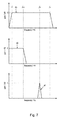
The first stage 12 has a frequency response 45 having a low frequency cut-off fl and a high frequency cut-off fu. Below the low frequency cut-off fl and above the high frequency cut-off fu the gain G of the first stags drops rapidly so that frequencies outside the range fl to fu are blocked. The high frequency cut-off fu is greater than the base-frequency fd of the periodic signal 43. The low-frequency cut-off is preferably at least 1 hertz, or at least sufficiently high to substantially block voltage signals resulting from a pyroelectric effect in the layer of piezoelectric material 10 which result from the body temperature of a user's digit. For application in an industrial or domestic environment, the low frequency cut-off fl may be at least 50 Hz, at least 60 Hz or at least sufficiently high to reject noise pick-up at a frequency of a domestic of industrial power distribution network and resulting from ambient electric fields. The low frequency cut-off fl may be at least 100 Hz. The low frequency cut-off fl may be at least 200 Hz. For application in aircraft, the low frequency cut-off fl may be at least 400 Hz.
Referring in particular to FIG. 7, the first frequency-dependent filter 13 may be a low-pass filter 46 having a cut-off frequency foff which is lower than the base frequency fd of the periodic signal 43, and the second frequency-dependent filter 14 may be a band-pass filter 47 having a pass-band including the base frequency fd.
Referring in particular to FIG. 8, the first frequency-dependent filter 13 may be a band-reject filter 48 having a stop-band including the base frequency fd, and the second frequency-dependent filter 14 may be a band-pass filter 47 having a pass-band including the base frequency fd.
Referring in particular to FIG. 9, the first frequency-dependent filter 13 may be a low-pass filter 46 having a cut-off frequency foff which is lower than the base frequency fd of the periodic signal 43, and the second frequency-dependent filter 14 may be a high-pass filter 49 having a cut-off frequency fon which is lower than the base frequency fd of the periodic signal 43 and higher than the cut-off frequency foff of the first frequency-dependent filter 13.
The band-pass filter 47 and/or the band-reject filter 48 may be notch filters or comb filters. If the periodic signal 43 has a sinusoidal waveform the band-pass filter 47 and/or the band-reject filter 48 are preferably notch filters centered at the base frequency fd. If the periodic signal 43 has a non-sinusoidal waveform, then the band-pass filter 47 and/or the band-reject filter 48 are preferably wide band-filters, or comb-filters having pass/reject bands centered at the base frequency fd and harmonics thereof.
The first and second frequency- dependent filters 13, 14 may be provided by active filter circuits. The first and second frequency- dependent filters 13, 14 may be provided by passive filter circuits. The first and second frequency- dependent filters 13, 14 may be provided by single stage filters or multiple stage filters. The first and second frequency- dependent filters 13, 14 may be Butterworth filters, Chebyshev filters, Gaussian filters and Bessel filters. The first frequency-dependent filter 13 may be of different type to the second frequency-dependent filter.
Alternatively, the second stage of the front end module 3 and the first and second frequency- dependent filters 13, 14 may be provided by an suitably programmed information processing device such as a microprocessor or a microcontroller.
Examples of circuits which may provide the first stage 12 in cases where the periodic signal 43 is received by the front end module 3 shall now be described.
First amplifier: Referring also to FIG. 10, a first amplifier 50 for the first stage 12 of the front end module 3 will be explained in a case where the signal source 44 is a voltage controlled source Vd(fd) which supplies the periodic signal 43 to the front end module 3.
The first touch sensor 2 is represented in the circuit diagram by an equivalent circuit 51 in which Cself represents the self capacitance of the first electrode 8, ΔCself represents the change in the self capacitance of the first electrode resulting from the touch or proximity of a user's digit or a conductive stylus. Csensor represents the mutual capacitance between the first and second electrodes 8, 9 and Psensor represents the piezoelectric response of the layer of piezoelectric material 10. The first electrode 8 is coupled to the terminal A and the second electrode 9 is coupled to a voltage bias source 52 which provides a constant bias voltage Vbias to the second electrode 9. The voltage bias Vbias may be a positive, negative or ground potential.
The first amplifier 50 provides the first stage 12 of the front end module 3. The first amplifier 50 includes an operational amplifier OP1 having at least an inverting input coupled to a first rail 53, a non-inverting input coupled to the voltage controlled source Vd(fd) via a path 54 including a first resistor Rd, and an output coupled to a second rail 55. The first amplifier 50 also includes a second resistor Ri coupling the first rail 53 to the terminal A. In this way, the first amplifier 50 is coupled to the first electrode 8. The first amplifier 50 also includes a third resistor Rf coupling the first rail 53 to the second rail 55, and a first capacitor Cf coupling the first rail 53 to the second rail 55. Optionally, a second capacitor Cd may be connected in parallel with the first resistor Rd. Other terminals of the operational amplifier OP1, such as power supply terminals, may be present but are not shown in this or other schematic circuit diagrams described herein.
The gain and frequency dependence of the first amplifier 50 are controlled by the third resistor Rf and the first capacitor Cf which provide a negative feedback network to the operational amplifier OP1. In the first amplifier 50, the second rail 55 provides the amplified signal 15 via an output terminal Vout. Alternatively, the second rail 55 may be directly coupled to the second stage of the front end module 3.
Because the non-inverting input of the operational amplifier OP1 is coupled to the voltage controlled source Vd(fd), the amplifier is effectively provided with a periodically varying virtual earth. In this way, the amplified signal 15 output by the first amplifier 50 is modulated by the periodic signal 43, and includes a superposition of the integrated output voltage signal Vpiezo(t) and the capacitance measurement voltage signal Vcap(t). One simple way to view the interaction with the periodic signal 43 is using one of the “Golden rules” of operational amplifiers, namely that when an ideal operational amplifier is provided with a negative feedback network, the inverting and non-inverting inputs will be at the same potential. Thus, the potential at the non-inverting input of the operational amplifier OP1 varies with the periodic signal 43, and couples to the capacitances of the equivalent circuit 51. Coupling the periodic signal 43 to the capacitances of the equivalent circuit 51 using the described virtual earth configuration may have the advantage of allowing higher gains to be used to amplify the current signal Ipiezo(t) without saturating the output of the operational amplifier OP1.
The capacitance of the first capacitor Cf may be selected to be approximately equal to the mutual capacitance Csensor between the first electrode 8 and the second electrode 9. The low frequency cut-off fl of the first amplifier 50 may be approximated as fl=1/(2π×Rf×Cf). The high frequency cut-off fu may be approximated as fu=1/(2π×Ri×Cf). In this way, the second and third resistors Ri, Rf and the first capacitor Cf may be selected such that the high frequency cut-off fu is greater than the base frequency fd of the periodic signal 43 and the low-frequency cut-off is at least 1 hertz or at least sufficiently high to substantially block voltage signals resulting from a pyroelectric effect in the layer of piezoelectric material 10. Optionally, the low frequency cut-off fl may be at least 50 Hz or at least 60 Hz or at least sufficiently high to reject noise pick-up at a frequency of a domestic or industrial power distribution network.
The voltage bias source 52 need not provide a constant bias voltage Vbias, and the voltage bias source 52 may instead provide a time varying voltage. In some cases, the voltage bias source 52 may alternatively be provided by the signal source 44 such that the periodic signal 43 is provided to the second electrode 9.
The equivalent circuit 51 has been shown as including a variable capacitance ΔCself arising from self capacitance of the first electrode 8. However, the equivalent circuit 51 of the touch sensor 2 may additionally or alternatively include a variable capacitance ΔCsensor arising from a mutual capacitance between the first and second electrodes 8, 9. In general, the equivalent circuit 51 may be different depending on the exact geometries of the first and second electrodes 8, 9 and the touch sensor 2.
Referring also to FIG. 11, the first amplifier 50 may provide the first stages 12 of the first and second front end modules 3 a, 3 b for the second apparatus 20.
A pair of first amplifiers 50 a, 50 b may provide the first stage of the respective front end modules 3 a, 3 b of the second apparatus 20 in a similar way to the first apparatus 1. The input to a first amplifier 50 a which is included in the first front end module 3 a is coupled via terminal D to the first electrode 8 of the second touch sensor 21. The input to a first amplifier 50 b which is included in the second front end module 3 b is coupled via terminal C to the third electrode 26 of the second touch sensor 21. The second electrode 9 of the second touch sensor 21 is coupled via terminal E to a voltage bias source 52. The same voltage controlled source 44, Vd(fd) may be coupled to both front end modules 3 a, 3 b in parallel.
Thus, each first amplifier 50 a, 50 b provides a corresponding amplified signal 15 a, 15 b depending upon input signals 11 a, 11 b from the first and third electrodes 8, 26 respectively. One difference to the first touch sensor 2 is that the equivalent circuit 56 of the second touch sensor 21 also includes a mutual capacitance Cmut between the first electrode 8 and the third electrode 26.
Second amplifier: Referring also to FIG. 12, a second amplifier 57 for the first stage 12 of the front end module 3 will be explained in a case where the signal source 44 is a voltage controlled source Vd(fd) which supplies the periodic signal 43 to the front end module 3.
The first touch sensor 2 is represented in the circuit diagram by an equivalent circuit 51. The first electrode 8 is coupled to the terminal A and the second electrode 9 is coupled to a voltage bias source 52 which provides a constant bias voltage Vbias to the second electrode 9. The voltage bias Vbias may be a positive, negative or ground potential.
The second amplifier 57 includes a first operational amplifier OP1 having at least an inverting input coupled to a first rail 58, a non-inverting input coupled to the voltage controlled source Vd(fd) via a path including a first resistor Rd1 and a second rail 59, and an output coupled to a third rail 60. The second amplifier 57 includes a second operational amplifier OP2 having at least an inverting input coupled to a fourth rail 61, a non-inverting input coupled to the second rail 59 via a path including a second resistor Rd2, and an output coupled to a fifth rail 62. The second amplifier includes a comparator CM1 having at least an inverting input coupled to the third rail 60, a non-inverting input coupled to the fifth rail 62, and an output providing the amplified signal 15. The second amplifier 57 also includes a third resistor Ri1 coupling the first rail 53 to the terminal A, a fourth resistor Rf1 coupling the first rail 58 to the third rail 60, a first capacitor Cf1 coupling the first rail 58 to the third rail 60, a fifth resistor Rf2 coupling the fourth rail 61 to the fifth rail 62, a second capacitor Cf2 coupling the fourth rail 61 to the fifth rail 62, and a sixth resistor Ri2 coupling the fourth rail 61 to ground via a path 63 including a third capacitor Cref.
The first resistor Rd1 may have a resistance substantially equal to the second resistor Rd2. The fourth resistor Rf1 may have a resistance substantially equal to the fifth resistor Rf2. The first capacitor Cf1 may have a capacitance substantially equal to the second capacitor Cf2, and also approximately equal to a mutual capacitance Csensor between the first electrode 8 and the second electrode 9. The third capacitor Cref may have a capacitance approximately equal to a mutual capacitance Csensor between the first electrode 8 and the second electrode 9. A fourth capacitor Cd1 may be connected in parallel with the first resistor Rd1. A fifth capacitor Cd2 may be connected in parallel with the second resistor Rd2.
The second amplifier 57 operates in substantially the same way as the first amplifier 50, except that the second amplifier 57 is a differential amplifier which ideally provides an amplified signal 15 which has zero or negligible amplitude when there is no user interaction with the touch sensor 2.
Referring also to FIGS. 2 and 11, the second amplifier 57 may be used in the second apparatus in the same way, as the first amplifier 50 by connecting the respective inputs of a pair of second amplifiers 57 to the first and third electrodes 8, 26 of the second touch sensor 21 via the terminals D and C respectively.
Third amplifier: Referring also to FIG. 13, a third amplifier 63 for the first stage 12 of the front end module 3 will be explained in a case where the signal source 44 is a current controlled source Id(fd) which supplies the periodic signal 43 to the front end module 3.
The first touch sensor 2 is represented in the circuit diagram by the equivalent circuit 51. The first electrode 8 is coupled to the terminal A and the second electrode 9 is coupled to the terminal B. Both the terminal A and terminal B are coupled to the third amplifier 63.
The third amplifier 63 includes an operational amplifier OP1 having at least an inverting input coupled to the current controlled source Id(fd) via in first rail 63, a non-inverting input coupled to ground via a path 65 including a first resistor Rd, and an output coupled to a second rail 66. The third amplifier 63 also includes a second resistor (Rf) coupling the first, rail 64 to the second rail 66, and a third resistor Ri coupling the first rail 64 to ground via a path including a first capacitor Cf. In the third amplifier 63, the second rail 66 provides the amplified signal 15.
The first rail 64 is coupled to the first electrode 8 via terminal A and the second rail 66 is coupled to the second electrode 9 via terminal B. Alternatively, the first rail 64 may be coupled to the second electrode 9 via terminal B and the second rail 66 may be coupled to the first electrode 8 via terminal A.
A second capacitor Cd may be connected in parallel with the first resistor Rd. The first capacitor Cf may have a capacitance substantially equal to a mutual capacitance Csensor between the first electrode 8 and the second electrode 9.
In many respects, for example the high and low frequency cut-offs fl, fu, the third amplifier 63 is configured similarly to the first and second amplifiers 50, 57. However, the feedback network of the third amplifier 63 differs from the first or second amplifiers 50, 57 because it includes the first touch sensor 2.
The second apparatus 20 may use front end modules 3 a, 3 b which have first stages 12 provided by the third amplifier 63. A third amplifier 63 included in the first front end module 3 a may be connected across the terminals D and E instead of A and B, and a third amplifier 63 included in the second front end module 3 b may be connected across the terminals C and E. Optionally, a third front end module (not shown) may be used which includes a third amplifier 63 connected across the terminals C and D. When more than one third amplifier 63 is used, each third amplifier 63 should be coupled to the output of a separate, synchronised current controlled source Id(fd).
Fourth amplifier: Referring also to FIG. 14, a fourth amplifier 67 for the first stage 12 of the front end module 3 will be explained in a case where the signal source 44 is a pair of synchronised current controlled sources Id1(fd), Id2(fd) which supply the periodic signal 43 to the front end module 3.
The first touch sensor 2 is represented in the circuit diagram by the equivalent circuit 51. The first electrode 8 is coupled to the terminal A and the second electrode 9 is coupled to the terminal B. Both terminal A and terminal B are coupled to the third amplifier 63.
The fourth amplifier 67 includes a first operational amplifier OP1 having at least an inverting input coupled to a first current controlled source Id1(fd) via a first rail 68, a non-inverting input coupled to ground via a path 69 including a first resistor Rd1, and an output coupled to a second rail 70. The fourth amplifier 67 also includes a second operational amplifier OP2 having at least an inverting input coupled to a second current Id2(fd) source by a third rail 71, a non-inverting input coupled to ground visa path 72 including a second resistor Rd2, and an output coupled to a fourth rail 73. The fourth amplifier 67 also includes a comparator CM1 having at least an inverting input coupled to the second rail 70, a non-inverting input coupled to the fourth rail 73, and an output providing the amplified signal 15. The fourth amplifier 67 also includes a third resistor Rf1 coupling the first rail 68 and the second rail 70, a fourth resistor Ri1 coupling the first rail 68 to ground via a path including a first capacitor Cf1, a fifth resistor Ri2 coupling the third rail 71 to ground via a path including a second capacitor Cf2, a sixth resistor Rf2 coupling the third rail 71 to the fourth rail 73, and a third capacitor Cref coupling the third rail 71 to the fourth rail 73. The first current controlled source Id1(fd) is synchronised with the second current controlled source Id2(fd).
The first rail 68 is coupled to the first electrode 8 via terminal A and the second rail 70 is coupled to the second electrode 9 via terminal B. Alternatively, the first rail 68 may be coupled to the second electrode 9 via terminal B and the second rail 70 may be coupled to the first electrode 8 via terminal A.
The first resistor Rd1 may have a resistance substantially equal to the second resistor Rd2. The third resistor Rf1 may have a resistance substantially equal to the sixth resistor Rf1. The first capacitor Cf1 may have a capacitance substantially equal to the second capacitor Cf2 and approximately equal to a mutual capacitance Csensor between the first electrode 8 and the second electrode 9. The third capacitor Cref may have a capacitance approximately equal to a mutual capacitance Csensor between the first electrode 8 and the second electrode 9. A fourth capacitor Cd1 may be connected in parallel with the first resistor Rd1. A fifth capacitor Cd2 may be connected in parallel with the second resistor Rd2.
The fourth amplifier 67 operates in substantially the same way as the third amplifier 63, except that the fourth amplifier 67 is a differential amplifier which ideally provides an amplified signal 15 which has zero or negligible amplitude when user does not touch and/or press the touch sensor 2.
The second apparatus 20 may use front end modules 3 a, 3 b which each have a first stage 12 provided by the fourth amplifier 67. A fourth amplifier 67 included in the first front end module 3 a may be connected across the terminals D and G instead of A and B as shown in FIG. 14, and a fourth amplifier 67 included in the second front end module 3 b may be connected the terminals C and E. Optionally, a third front end module (not shown) may be used which includes a fourth amplifier 67 connected across the terminals C and D.
Third combined capacitance and pressure sensing apparatus and first touch panel: Referring also to FIGS. 15 and 16, a third apparatus 74 including a first touch panel 29, a first touch controller 30 and a multiplexer 75 will be explained.
The multiplexer 75 has a plurality of inputs and one output, the output is coupled to a terminal F.
The first touch panel 29 includes a layer structure 5 which is generally the same as the layer structure of the first touch sensor 2, except that the layer structure 5 of the first touch panel 29 is shared between multiple first electrodes 8 disposed on the first face 6 in the form of pads of conductive material. The first electrodes 8 are disposed on the first face 6 in an array extending in the first and second directions x, y. Each first electrode 8 is coupled to a corresponding input of the multiplexer 75 by a respective conductive trace 76. The conductive traces 76 may be made of the same material as the first electrodes 8. Alternatively, the conductive traces 76 may be made of a material having a higher conductivity than the material used for the first electrodes 8. The conductive traces 76 are generally much thinner in the plane defined by the first and second directions x, y than the corresponding first electrodes 8. The second electrode 9 is disposed on the second face 9 and is extensive such that the second electrode at least partial underlies each first electrode 8. The second electrode 9 may be substantially coextensive with the second face 7. The second electrode is coupled to a terminal G.
In this way, each first electrode 8 effectively provides a first touch sensor 2 which may be individually addressed using the multiplexer 75 and the conductive traces 76.
The first touch panel 29 may be bonded overlying the display 37 of an electronic device 28. In this case, the materials of the first touch panel 29 should be substantially transparent as described hereinbefore. A cover lens 77 may be bonded overlying the first touch panel 29. The cover lens 77 is preferably glass but may be any transparent material. The coyer lens 77 may be bonded to the touch panel 29 using a layer of PSA material 78. The layer of PSA material 78 may be substantially transparent. The array of first electrodes 8 mid the corresponding conductive traces 76 may be fabricated using index matching techniques to minimise visibility to a user.
The first touch controller 30 includes a front end module 3, a signal processing module 4 and a controller 79. The controller 79 may communicate with the processor 32 of the electronic device 28 using a link 80. The touch controller 30 may include a signal source 44 providing the periodic signal 43 to the front end module 3.
The front end module 3 is coupled to the output of the multiplexor 75 by the terminal F. In this way, the front end module 3 may receive an input signal 11 from any one of the first electrodes 8 which is addressed by the multiplexer 75. The front end module 3 may include a first stage 12 provided by any one of the first, second, third or fourth amplifiers 50, 57, 63, 67. Alternatively, the front end module 3 may include a first stage 12 using any circuit which provides an amplified signal 15 based on the input signal 11 and including a superposition of the integrated output voltage signal Vpiezo(t) and the capacitance measurement voltage signal Vcap(t) as hereinbefore described.
In a case where the front end module 3 includes the first or second amplifiers 50, 57, the second electrode 9 may be coupled to a bias voltage source 52 via the terminal G. Alternatively, in a case when the front end module 3 includes the third or fourth amplifiers 63, 67, the second electrode 9 may be coupled to the front end module 3 via the terminal G.
The controller 79 may provide a control signal 81 to the multiplexer 75. The control signal 81 may cause the multiplexer 75 to address each input according to a sequence determined by the controller 79. In this way, the from end module 3 may receive an input signal 11 from each first electrode 8 according to a sequence determined by the controller 80. The sequence may be pre-defined, for example, the sequence may select each first electrode 8 once before repeating. The sequence may be dynamically determined, for example, when one or more user interactions are detected, the controller 79 may scan the subset of first electrodes 8 adjacent to each detected user interaction in order to provide faster and/or more accurate tracking of user touches. The sequence may be arranged so that the multiplexor 75 addresses each first electrode 8 during a quiet period or blanking period of the display 37. The sequence may be provided to the controller 79 by the processor 32 via the link 80. Alternatively, the processor may directly control the sequence via the link 80.
In this way, the front end module 3 may receive input signals 11 from each of the first electrodes 8 which are disposed in an array extending in the first and second directions. The signal processing module 4 provides respective pressure values 18 and capacitance values 19 to the controller. The controller 79 uses the received pressure values 18 and capacitance values 19 to calculate a position and an applied pressure for one or more user interactions with the touch panel 29. The controller 79 provides the positions and/or pressures of one or more user interactions to the processor 32 as input information via the link 80. Alternatively, the pressure values 18 and capacitance values 19 may be provided to the processor 32 via the link 80 and the processor 32 may calculate the positions and/or pressures of one or more user interactions. The controller 79 or the processor 32 are calibrated by applying known pressures to known locations so that the accuracy of calculated positions and/or pressures of one or more user interactions may be optimised and/or verified.
Referring also to FIG. 17, a configuration of the first amplifier 50 included in the third apparatus 74 is shown.
The configuration of the first amplifier 50 included in the third apparatus 74 is substantially the same as the configuration of the first amplifier 50 included in the first apparatus 1, except that the first rail 53 is coupled to the output of the multiplexor 75 via the terminal F instead of being coupled to the terminal A, the voltage bias source 52 is coupled to the second electrode 9 via the terminal G instead of the terminal B, and that the first amplifier 50 further includes a switch SW1.
The switch SW1 is coupled between the first rail 53 and the second rail 55 of the first amplifier 50. When the switch SW1 is closed, the first capacitor C-f of the first amplifier 50 is discharged. The opening and closing of the switch SW1 may be governed by a control signal 82 provided by the controller 79. In this way, after an input signal 11 has been received from one of the first electrodes 8, the first capacitor Cf may be discharged in order to reset the feedback network of the first amplifier 50 before the multiplexer 75 addresses a different first electrode 8.
Referring also to FIG. 18, a configuration of the second amplifier 57 included in the third apparatus 74 is shown.
The configuration of the second amplifier 57 included in the third apparatus 74 is substantially the same as the configuration of the first amplifier 50 included in the third apparatus 74, except that the second amplifier 57 is used instead of the first amplifier 50 and the second amplifier 57 further includes a first switch SW1 and a second switch SW2.
The first switch SW1 couples the first rail 58 to the third rail 60 of the second amplifier 57 and the second switch SW2 couples the fourth rail 61 to the fifth rail 62. When the switch SW1 is closed, the first capacitor C-f 1 of the second amplifier 57 is discharged. When the switch SW2 is closed, the second capacitor C-f 2 of the second amplifier 57 is discharged. The opening and closing of the switches SW1, SW2 may be governed by control signals 82 provided by the controller 79. In this way, after an input signal 11 has been received from one of the first electrodes 8, the capacitors Cf1, Cf2 may be discharged so as to reset the feedback network of the second amplifier 57 before the multiplexer 75 addresses a different first electrode 8.
Alternatively, the third apparatus 74 may include the third amplifier 63. In such a case, the first rail 64 of the third amplifier 63 may be coupled to the output of the multiplexor 75 via terminal F and the second rail 66 of the third amplifier 63 may be coupled to the second electrode 9 via terminal G. Alternatively, the first rail 64 of the third amplifier 63 may be coupled to the second electrode 9 via terminal G and the second rail 66 of the third amplifier 63 may be coupled to output of the multiplexor 75 via terminal F.
Alternatively, the third apparatus 74 may include the fourth amplifier 67. In such a case, the first rail 68 of the fourth amplifier 67 may be coupled to the output of the multiplexor 75 via terminal F and the second rail 70 of the fourth amplifier 67 may be coupled to the second electrode 9 via terminal G. Alternatively, the first rail 68 of the fourth amplifier 67 may be coupled to the second electrode 9 via terminal G and the second rail 70 of the fourth amplifier 67 may be coupled to the multiplexor 75 via terminal F.
When a user interacts with the first touch panel 29 proximate to a given first electrodes 8, the resulting change in capacitance of the respective touch sensor 2 formed by the given first electrode 8, the local region of the layer structure 5 and the local region of the second electrode 9, is mostly due to a change in the self-capacitance of the first electrode 8. This is because the magnitude of the mutual capacitance Csensor between the first electrode 8 and the second electrode 9 may be large such that a change in the mutual capacitance is relatively small. The value of the mutual capacitance Csensor between the first electrode B and the second electrode 9 may be reduced if required by using a patterned second electrode 9. Using a patterned second electrode 9 may allow the second electrode 9 to be disposed between a user's digit/stylus and the first and/or third electrodes 8, 26 without screening electrostatic interactions between the user's digit/stylus and the first and/or third electrodes 8, 26.
Referring also to FIG. 19, a patterned second electrode 83 is in the from of a Cartesian grid. The conductive region of the patterned second electrode 83 includes struts 84 extending in the first direction x and having a width W in the second direction y, and struts 85 extending in the second direction y and having a width W in the first direction x. The struts 84 extending in the first direction x are evenly spaced in the second direction y with a spacing S, and the struts 85 extending in the second direction y are evenly spaced in the first direction x with the same spacing S. The struts 84, 85 are joined where they intersect such that the patterned second electrode 83 is formed of a single region of conductive material.
The patterned second electrode 83 may be arranged such that the magnitude of the mutual capacitance Csensor between the first electrode 8 and the second electrode 9 is reduced. This may increase the relative size of changes in the mutual capacitance ΔCsensor between the first electrode 8 and the second electrode 9 resulting from a user's touch, making such changes ΔCsensor easier to detect.
Referring also to FIG. 20, using pressure values to infer a location and/or pressure of a user interaction occurring between two first electrodes 8 will be explained.
The separation between adjacent electrodes in a projected capacitance touch panel, sometimes referred to as the pitch, may be relatively coarse, for example, 1 to 5 mm or larger than 5 mm. If the positions of user interactions were determined only at the pitch length, projected capacitance touchscreens would not be able to provide accurate positions of user interactions or to smoothly follow a path traced by a user. To provide more accurate locations, projected capacitance touchscreens employ interpolation, for example, using an electrode having a peak signal and also the adjacent electrode signals, in order to infer a touch location using linear interpolation, quadratic interpolation or interpolation using higher order polynomials or other suitable functions. Such interpolation is possible because a user interaction may alter the capacitances of several adjacent electrodes simultaneously.
Similarly, when a user presses on the cover lens 77, the layer of piezoelectric material 10 underlying the cover lens 77 will experience strain across a broader area because of the rigidity of the cover lens 77. For example, a user interaction at a precise location 86 may result in pressure values 87 a and 87 b being calculated for first electrodes 8 at locations 88 a, 88 b which bracket the precise location 86. A user interaction al a precise location 86 may also result in pressure values 89 a and 89 b being calculated for first electrodes 8 at locations 90 a, 90 b adjacent to the pair of bracketing locations 88 a, 88 b.
The controller 79 or the processor 32 may calculate an estimate of the precise location 86 and/or a precise pressure value 91 using the largest value 87 a and the corresponding location 88 a in combination with the two next nearest values 87 b, 89 a and the corresponding locations 88 b, 90 a. Alternatively, the controller 79 or the processor 32 may calculate an estimate of the precise location 86 and/or a precise pressure value 91 using the pair of bracketing values 87 a, 87 b and locations 88 a, 88 b. The controller 79 or the processor 32 may calculate an estimate of the precise location 86 and/or a precise pressure value 91 using the pair of bracketing values 87 a, 87 b and locations 88 a, 88 b and the adjacent values and locations 89 a, 89 b, 90 a, 90 b. The controller 79 or the processor 32 may calculate an estimate of the precise location 86 and/or a precise pressure value 91 using linear interpolation, quadratic interpolation or interpolation using higher order polynomials or other suitable functions.
The third apparatus 73 may operate using interpolation of capacitance values 19 and/or pressure values 18 to determine locations and pressures of one or more user interactions.
Fourth combined capacitance and pressure sensing apparatus and second touch panel: Referring also to FIGS. 21 and 22, a fourth apparatus 93 including a second touch panel 92, a first touch controller 30 and a multiplexer 75 will be explained.
The fourth apparatus 93 is substantially the same as the third apparatus 74, except that the fourth apparatus 93 includes a second touch panel 92 instead of the touch panel 29.
The second touch panel 92 includes a layer structure 5 which is generally the same as the layer structure 5 of the second touch sensor 21, except that in the touch panel 92, the layer structure 5 is shared by multiple first electrodes 8 disposed on the first face 6 of the layer structure 5, and the second layer structure 23 is shared by multiple third electrodes 26 disposed on the third face 24 of the second layer structure 23. The first electrodes 8 each extend in the first direction x and the first electrodes 8 are disposed in an array evenly spaced in the second direction y. The third electrodes 26 each extend in the second direction y and the third electrodes 26 are disposed in an array evenly spaced in the first direction x. Each first electrode 8 and each third electrode 26 is coupled to a corresponding input of the multiplexer 75 by a respective conductive trace 76. The second electrode 9 is disposed on the second face 9 and is extensive such that the second electrode at least partially underlies each first electrode 8 and each third electrode 26. The second electrode 9 may be substantially coextensive with the second face 7. The second electrode is coupled to a terminal G.
In this way, the area around each intersection of a first electrode 8 with a third electrode 26 effectively provides a second touch sensor 21 and each of the first and third 8, 26 electrodes may be individually addressed using the multiplexer 75 and the conductive traces 76.
The second touch panel 92 may be bonded overlying the display 37 of an electronic device 28 and a cover lens 77 may be bonded overlying the second touch panel 92 in the same way as for the touch panel 29.
The controller 79 may provide a control signal 81 to the multiplexer 75 in the same way as for the third apparatus 74. However, in the fourth apparatus 93, the control signal 81 may cause the multiplexer 75 to address each input according to a different sequence to the third apparatus 74. For example, the control signal 81 may cause the multiplexer 75 to address a given first electrode 8, and to subsequently address each third electrode 26 intersecting the given first electrode 8 before addressing a further first electrode 8 and repeating the scan through the third electrodes 26. The control signal 81 may cause the multiplexer to dynamically address first and third electrodes 8, 26 proximate to first and third electrodes 8, 26 at which a user touch was previously detected.
In this way, a raster scan of the first and third electrodes 8, 26 may be performed which allows the first touch controller 30 to determine the positions and/or pressures of one or more user interactions.
In the similar way to the third apparatus 74, the changes in capacitance values 19 generated in the fourth apparatus in response to user interactions may be predominantly due to changes in self-capacitance of the addressed first or second electrode 8, 26. However, if a given pair of first and third electrodes 8, 26 are addressed sequentially and without excessive delay, a change in the mutual capacitance between the given pair of first and third electrodes 8, 26 may additionally be determined.
Although the first electrode 8 and the third electrode 26 have been shown as being substantially rectangular, other shapes can be used.
Referring also to FIG. 23, an alternative arrangement of the first and third electrodes 8, 26 is shown. Instead of being rectangular, each first electrode 8 may include several pad segments 94 evenly spaced in the first direction x and connected to one another in the first direction x by relatively narrow bridging segments 95. Similarly each third electrode 26 may comprise several pad segments 96 evenly spaced in the second direction y and connected to one another in the second direction y by relatively narrow bridging segments 97. The pad segments 94 of the first electrodes 8 are diamonds having a first width W1 in the second direction 7 and the bridging segments 95 of the first electrodes 8 have a second width W2 in the second direction y. The pad segments 96 and bridging segments 97 of the third electrodes 26 have the same respective shapes and widths W1, W2 as the first electrodes 8.
The first electrodes 8 and the third electrodes 26 are arranged such that the bridging segments 97 of the third electrodes 26 overlie the bridging segments 95 of the first electrodes 8. Alternatively, the first electrodes 8 and the third electrodes 26 may be arranged such that the pad segments 96 of the third electrodes 26 overlie the pad segments 94 of the first electrodes 8. The pad segments 94, 96 need not be diamond shaped, and may instead be circular. The pad segments 94, 96 may be a regular polygon such as a triangle, square, pentagon or hexagon. The pad segments 94, 96 may be I shaped or Z shaped.
Third touch panel: Referring also FIG. 24, a third touch panel 98 may be included in the fourth apparatus 93 instead of the second touch panel 92.
The third touch panel 98 is substantially the same as the second touch panel 92 except that the third touch panel 98 does not include the second layer structure 23 and the third electrodes 26 are disposed on the first face 6 of the layer structure 5 in addition to the first electrodes 8. Each first electrode 8 is a continuous conductive region extending in the first direction x in the same way as the second touch panel 92, for example, each first electrode 8 may include several pad segments 94 evenly spaced in the first direction x and connected to one another in the first direction x by relatively narrow bridging segments 95. Each third electrode 26 may comprise several pad segments 99 evenly spaced in the second direction y in the same way as the second touch panel 92. However, unlike the second touch panel 92, the pad segments 99 of the third touch panel are disposed on the first face 6 of the layer structure 5 and are interspersed with, and separated by, the first electrodes 8. The pad segments 99 corresponding to each third electrode 26 are connected together by conductive jumpers 100. The jumpers 100 each span a part of a first electrode 8 and the jumpers 100 are insulated from the first electrodes 8 by a thin layer of dielectric material (not shown) which may be localised to the area around the intersection of the juniper 100 and the first electrode 8.
Alternatively, a dielectric layer (not shown) may overlie the first face 6 of the layer structure 5 and the first and third electrode 8, 26. Conductive traces (not shown) extending in the second direction y may be disposed over the dielectric layer (not shown), each conductive trace (not shown) overlying the pad segments 99 making up one third electrode 26. The overlying conductive traces (not shown) may connect the pad segments 99 making up each third electrode 26 using vias (not shown) formed through the dielectric layer (not shown).
Fifth combined capacitance and pressure sensing apparatus: Referring also to FIG. 25, a fifth apparatus 93 including a second touch panel 92, a second touch controller 102 and first and second multiplexers 75 a, 75 b will be explained.
The first multiplexer 75 a has a plurality of inputs and an output coupled to the terminal H. The second multiplexer 75 b has a plurality of inputs and an output coupled to the terminal I.
The second touch panel 92 of the fifth apparatus 101 is the same as the second touch panel 92 of the fourth apparatus 93, except that each of the first electrodes 8 is coupled to a corresponding input of the first multiplexor 75 a by a respective first conductive trace 76 a, each of the third electrodes 26 is coupled to a corresponding input of the second multiplexer 75 b by a respective second conductive trace 76 b, and the second electrode 9 is coupled to a terminal J.
The second touch controller 102 includes the first and second front end modules 3 a, 3 b, the second signal processing module 22 and the controller 79. Each of the first and second front end modules 3 a, 3 b is substantially the same as the front end module 3 of the third and fourth apparatuses 74, 93. The second signal processing module 22 is substantially the same as the second signal processing module 22 of the second apparatus 20. The controller 79 is substantially the same as the controller 79 of the third of fourth apparatuses 74, 93, except that the control signals 81 may cause the first and second multiplexers 75 a, 75 b to address each given pair of first and third electrodes 8, 26 according to a sequence determined by the controller 79 or communicated to the controller 79 from the processor 32 by the link 80. The sequence may be a predetermined sequence or a dynamically determined sequence.
In this way, each intersection of the first and third electrodes 8, 26 effectively provides a second touch sensor 21 which may be individually addressed by the first and second multiplexers 75 a, 75 b. When a particular intersection is addressed by the first and second multiplexers 75 a, 75 b, a first input signal 11 a from the respective first electrode 8 is received by the first front end module 3 a and a second input signal 11 b from the respective third electrode 26 is concurrently received by the second front end module.
Alternatively, the fifth apparatus 101 may use the third touch panel 98 instead of the second touch panel 92.
In addition to changes in the self-capacitances of given first and third electrode 8, 26 addressed by the multiplexers 75 a, 75 b, the respective capacitance values 19 a, 19 b also include a change in the mutual capacitance between the addressed pair of first and third electrodes 8, 26.
Referring also to FIG. 26, a configuration using first amplifier 50 to provide the first stages 12 a, 12 b of the first and second front end modules 3 a, 3 b will be explained.
A configuration of the fifth apparatus 101 including the first amplifier 50 is substantially the same as the configuration of the third or fourth apparatuses 74, 93 including the first amplifier 50, except that a pair of multiplexers 75 a, 75 b, a pair of front end modules 3 a, 3 b and a pair of first amplifiers 50 a, 50 b are used, and in that the first amplifiers 50 a, 50 b further include a first switch SW1 and a second switch SW2.
The pair of first amplifiers 50 a, 50 b provide the first stages 12 a, 12 b of the first and second front end modules 3 a, 3 b respectively. The first rail 53 of the first amplifier 50 a which is included in the first front end module 3 a is coupled via the terminal H to the output of the first multiplexer 75 a. The first rail 53 of the first amplifier 50 b which is included in the second front end module 3 b is coupled via the terminal I to the output of the second multiplexer 75 b. The second electrode 9 of the second or third touch panels 92, 98 is coupled via terminal J to the voltage bias source 52. The same voltage controlled source Vd(fd) may be coupled to both front end modules 3 a, 3 b in parallel.
The pair first amplifiers 50 a, 50 b include a first switch SW1 and a second switch SW2. The first switch SW1 couples the first rail 53 to the second rail 55 of the first amplifier 50 s included in the first front end module 3 a. The second switch SW2 couples the first rail 53 to the second rail 55 of the first amplifier 50 b included in the second front end module 3 b. When the switch SW1 is closed, the first capacitor C-f of the first amplifier 50 a is discharged. When the switch SW2 is closed, the first capacitor C-f of the first amplifier 50 b is discharged. The opening and closing of the switches SW1, SW2 may be governed by control signals 82 provided by the controller 79. In this way, after the first front end module 3 a has received, an input signal 11 from one of the first electrodes 8 and the second front end module 3 b has received an input signal 11 from one of the third electrodes 26, the capacitors Cf of the first amplifiers 50 a, 50 b may be discharged so as to reset the respective feedback networks before the multiplexers 75 a, 75 b connect a different pairing of first and third electrodes 8, 26.
Thus, each first amplifier 50 a, 50 b provides a corresponding amplified signal 15 a, 15 b depending upon first and second input signals 11 a, 11 b received from the first and third electrodes 8, 26 addressed by the respective first and second multiplexers 75 a, 75 b. One difference to the third or fourth apparatuses 74, 93 is that the equivalent circuit 56 of each second touch sensor 21 provided by an addressed pair of first and second electrodes 8, 26 additionally includes a mutual capacitance Cmut between the selected first electrode 8 and the selected third electrode 26.
Alternatively, the fifth apparatus 102 may be configured using first and second front end modules 3 a, 3 b including respective second amplifiers 57. In such a case, the first rail 58 of the second amplifier 57 included in the first front end module 3 a may be coupled to the output of the first multiplexer 75 a via the terminal H, the first rail 58 of the second amplifier 57 included in the second frontend module 3 b may, be coupled to the output of the second multiplexer 75 b via the terminal I, and the second electrode 9 of the second or third touch panels 92, 98 may be coupled via terminal J to a voltage bias source 52.
Alternatively, the fifth apparatus 102 may be configured using first and second front end modules 3 a, 3 b including respective third amplifiers 63. In such a case, the first rail 64 of the third amplifier 63 included in the first front end module 3 a may be coupled to the terminal H and the corresponding second rail 66 may be coupled to the terminal J, and the first rail 64 of the third amplifier 63 included in the second front end module 3 b may be coupled to the terminal I and the corresponding second rail 66 may be coupled to the terminal J. Alternatively, the first rail 64 of the third amplifier 63 included in the first front end module 3 a may be coupled to the terminal J and the corresponding second rail 66 may be coupled to the terminal H, and the first rail 64 of the third amplifier 63 included in the second front end module 3 b may be coupled to the terminal J and the corresponding second rail 66 may be coupled to the terminal I.
Alternatively, the fifth apparatus 102 may be configured using first and second front end modules 3 a, 3 b including respective fourth amplifiers 67. In such a case, the first rail 68 of the fourth amplifier 67 included in the first front end module 3 a may be coupled to the terminal H and the corresponding second rail 70 may be coupled to the terminal J, and the first rail 68 of the fourth amplifier 67 included in the second front end module 3 b may be coupled to the terminal I and the corresponding second rail 70 may be coupled to the terminal J. Alternatively, the first rail 68 of the fourth amplifier 67 included in the first front end module 3 a may be coupled to the terminal J and the corresponding second rail 70 may be coupled to the terminal H, and the first rail 68 of the fourth amplifier 67 included in the second front end module 3 b may be coupled to the terminal J and the corresponding second rail 70 may be coupled to the terminal I.
Sixth combined capacitance and pressure sensing apparatus and fourth touch panel: Referring also to FIGS. 27 and 28, a sixth apparatus 104 including a fourth touch panel 103, a third touch controller 105 and first and second multiplexers 75 a, 75 b will be explained.
The sixth apparatus 104 includes first and second multiplexers 75 b, a fourth touch panel 103 and a third touch controller 105. In many respects the sixth apparatus 104 is substantially similar or analogous to the third to fifth apparatuses 74, 93, 101, and only the differences of the sixth apparatus 104 shall be explained.
The first and second multiplexers 75 a, 75 b each include a plurality of inputs and an output. The output of the first multiplexer 75 a is coupled to a terminal K and the output of the second multiplexer 75 b is coupled to a terminal L.
The fourth touch panel 103 includes a layer structure 5 which is generally the same as the layer structure 5 of the first touch sensor 1, except that in the fourth touch panel 103, the layer structure 5 is common to many first electrodes 8 disposed on the first face 6 of the layer structure 5 and many second electrodes 9 disposed on the second face 7 of the layer structure 5. The first electrodes 8 each extend in the first direction x and the first electrodes 8 are disposed in an array evenly spaced in the second direction y. The second electrodes 9 each extend in the second direction y and the second electrodes 9 are disposed in an array evenly spaced in the first direction x. Each second electrode 9 is coupled to a corresponding input of the first multiplexer 75 a by a respective conductive trace 76 a, and each first electrode 8 is coupled to a corresponding input of the second multiplexer 75 b by a respective conductive trace 76 b. In this way, the area around each intersection of a first electrode 8 with a second electrode 9 effectively provides a first touch sensor 2 and each of the first and second 8, 9 electrodes may be individually addressed using the first and second multiplexers 75 a, 75 b and the conductive traces 76 a, 76 b.
The fourth touch panel 103 may be bonded overlying the display 37 of an electronic device 28 and a cover lens 77 may be bonded overlying the fourth touch panel 103 in the same way as for the touch panel 29, the second touch panel 92 or the third touch panel 98.
The third touch controller 105 includes a front end module 3, a signal source 44, a signal processing module 4 and a controller 79 which are the same as hereinbefore described, except that the first stage 12 of the front end module 3 uses the third amplifier 63 of the fourth amplifier 67 and the signal source 44 is one or more synchronised current controlled sources Id(fd). In this case, the front end module 3 is connected across the terminals K and L.
The controller 79 may provide a control signal 81 to the first and second multiplexers 75 a, 75 b in the same way as for the fifth apparatus 101. In this way, each intersection of the first and third electrodes 8, 26 effectively provides a first touch sensor 2 which may be individually addressed by the first and second multiplexers 75 a, 75 b.
In addition to changes in the self-capacitances of given first and second electrodes 8, 9 addressed by the multiplexers 75 a, 75 b, the capacitance values 19 also include a change in the mutual capacitance between the addressed pair of first and second electrodes 8, 9.
Although the first electrode 8 and the third electrode 26 have been shown as being substantially rectangular, other shapes can be used. For example, the first and second electrodes 8, 9 of the fourth touch panel 103 may have shapes and configurations substantially similar to the first and third electrodes 8, 26 of the second touch panel 92.
Referring also to FIG. 29, a configuration of the third amplifier 63 included in the sixth apparatus 104 will be explained.
The first rail 64 of the third amplifier 63 may be coupled to the terminal K and the second rail 66 may be coupled to the terminal L. Alternatively, first rail 64 of the third amplifier 63 may be coupled to the terminal L and the second rail 66 may be coupled to the terminal K.
Alternatively, the fourth amplifier 67 may be included in the sixth apparatus 104. In such a case, the first rail 68 of the fourth amplifier 67 may be coupled to the terminal K and the second rail 70 may be coupled to the terminal L. Alternatively, first rail 68 of the fourth amplifier 67 may be coupled to the terminal L, and the second rail 70 may be coupled to the terminal K.
First display stack up: Referring also to FIGS. 30A to 30C, a first display stack-up 106 and a method of fabricating the first display stack 106 up will be explained.
Referring in particular to FIG. 30A, the cover tens 77 is a transparent substrate extending in the first x and second y directions and having first 77 a and second 77 b opposite faces. A first dielectric layer 107 extends in the first x and second y directions and has first 107 a and second 107 b opposite faces. Third electrodes 26 in the form of a set of conductive regions extending in the first direction x and spaced apart in the second direction y are disposed on the second face 107 b of the first dielectric layer 107. The second face 107 b of the first dielectric layer 107 is bonded to the first face 77 a of the cover lens 77.
Referring in particular to FIG. 30B, a second dielectric layer 108 extends in the first x and second y directions and has first 108 a and second 108 b opposite faces. First electrodes 8 in the form of a set of conductive regions extending in the second direction y and spaced apart in the first direction x are disposed on the second face 108 b of the second dielectric layer 108. The second face 108 b of the second dielectric layer 108 is bonded to the first face 107 a of the first dielectric layer 107.
Referring in particular to FIG. 30C, a layer of piezoelectric material 10 extends in the first x and second y directions and has first 10 a and second 10 b opposite faces. A second electrode 9 in the form of a conductive material region is disposed on the first face 10 a of the layer of piezoelectric material 10 such that, when assembled, the second electrode 9 at least partially overlaps each first electrode 8 and each third electrode 26 region. The second face 10 b of the layer of piezoelectric material 10 is bonded to the first face 108 a of the second dielectric layer 108.
The first display stack-up 106 may be bonded overlying the display 37 of an electronic device 28. The elements of the first display stack-up 106 are stacked in the thickness direction z from the display 37 to the cover lens 77. The layer structure 5 includes the second dielectric layer 108 and the layer of piezoelectric material 10 and the second layer structure 23 includes the first dielectric layer 108.
The cover lens 77 is made of glass, or PET or any oilier substantially transparent material. The cover lens 77 may be up to about 20 mm thick and may be at least 0.05 mm thick. Preferably, the cover lens 77 is up to about 2 mm thick and may be at least 0.05 mm thick. The layer of piezoelectric material 10 is made of PVDF or any other substantially transparent piezoelectric material. The layer of piezoelectric material 10 may be poled before assembling the first stack-up 106. Alternatively, the layer of piezoelectric material may be poled after assembling the first stack-up 106. The layer of piezoelectric material may be up to about 110 μm thick, and may be at least 0.5 μm or at least 1 μm thick. The second electrode 9 and the first electrodes 8 and/or third electrodes 26 may be used to produce a poling field. The dielectric layers 107, 108 may be PET or any other substantially transparent polymer. The dielectric layers 107, 108 may be between 10 μm and 100 μm thick, for example, around 20 to 25 μm thick. Preferably the dielectric layers 107, 108 are in the range of about 10-100 μm thick. The conductive regions providing the electrodes 8, 9, 26 may be ITO, IZO or any other substantially transparent conductive material. The conductive regions providing the electrodes 8, 9, 26 may be applied to the dielectric layers 107, 108 and/or the layer of piezoelectric material 10 using lithography, printing or other suitable methods. The shapes of the conductive regions providing the first, second and third electrodes 8, 9 26 may be any suitable electrode shape described in relation to one of the third to sixth apparatuses 74, 93, 101, 104. The sheet resistance of conductive regions providing electrodes may be between 1 and 200 Ω/sq. The sheet resistance may be below 10 Ω/sq. Preferably the sheet resistance is as low as is practical.
The assembly of the first display stack-up 106 has been described in a certain sequence. However, the elements of the first display stack-up may be bonded together in any other sequence resulting in the same ordering of layers 107, 108, 10. In particular, the first and second dielectric layers 107, 108 and the layer of piezoelectric material 10 may be bonded together using continuous roll-to-roll production methods before being bonded to the cover lens 77. When the cover lens 77 is a flexible material, the first display stack-up 106 may be fabricated entirely using continuous roll-to-roll processes.
The first display stack-up 106 does not require complex patterning of the layer of piezoelectric material 10 or of electrodes disposed on the layer of piezoelectric material 10. This allows fabrication of the first display stack-up to avoid complex multi-stage and/or duplex patterning of electrodes. As a result, fabrication of the first display stack-up 106 may be fast, efficient and cheap.
Second display stack up: Referring also to FIGS. 31A to 31C, a second display stack-up 109 and a method of fabricating the second display stack-up 109 will be explained.
The second display stack-up 109 is the same as the first display stack-up 106, except that elements of the second display stack-up 109 are bonded to one another using layers of pressure sensitive adhesive (PSA) material 110 extending in the first x and second y directions. For example, the cover tens 77 and the first dielectric layer 107 are arranged so that the first face 77 a of the cover lens 77 is opposite to and separated from the second face 107 b of the first dielectric layer 107. Pressure applied in the thickness direction z to bond the cover lens 77 and the first dielectric layer 107 together. Layers of PSA material 110 are used in the same way to bond the first and second dielectric layers 107, 108, to bond the second dielectric layer 108 to the layer of piezoelectric material 10 and to bond the second stack-up 109 overlying the display 37. Layers of PSA material 100 may be between 10 and 50 μm thick. Preferably, the layers of PSA material 110 are 25 μm thick.
The elements of the second display stack-up 109 are stacked in the thickness direction z from the display 37 to the cover lens 77. The layer structure 5 includes the second dielectric layer 108, the layer of piezoelectric material 10 and a layer of PSA material 110. The second layer structure 23 includes the first dielectric layer 107 and a layer of PSA material 110.
Third display stack-up: Referring also to FIGS. 32A to 32C, a third display stack-up 111 and a method of fabricating the third display stack-up 111 will be explained.
Referring in particular to FIG. 32A, the cover lens 77 is a transparent substrate extending in the first x and second y directions and having first 77 a and second 77 b opposite faces. A first dielectric layer 107 extends in the first x and second y directions and has first 107 a and second 107 b opposite faces. Third electrodes 26 in the form of a set of conductive regions extending in the first direction x and spaced apart in the second direction y are disposed on the second face 107 b of the first dielectric layer 107. The second face 107 b of the first dielectric layer 107 is bonded to the first face 77 a of the cover lens 77 using a layer of PSA material 110.
Referring in particular to FIG. 32B, a layer of piezoelectric material 10 extends in the first x and second y directions and has first 10 a and second 10 b opposite faces. First electrodes 8 in the form of conductive regions extending in a second direction y and spaced apart in the first direction x are disposed on the second face 10 b of the layer of piezoelectric material 10. A second electrode 9 in the form of a conductive material region is disposed on the first face 10 a of the layer of piezoelectric material 10 such that, when assembled, the second electrode 9 at least partially overlaps each first electrode 8 and each third electrode 26. The second face 10 b of the layer of piezoelectric material 10 may be bonded to the first face 107 a of the first dielectric layer 107 using a layer of PSA material 110.
Referring in particular to FIG. 32C, the third display stack up 111 may be bonded overlying the display 37 using a layer of PSA material 110.
The elements of the third display stack-up 111 are stacked in the thickness direction z from the display 37 to the cover lens 77. The layer structure 5 includes the layer of piezoelectric material 10. The second layer structure 23 includes the first dielectric layer 107 and a layer of PSA material 110.
Fourth display stack-up: Referring also to FIGS. 33A to 33D, a fourth display stack-up 112 and a method of fabricating the fourth display stack-up 112 will be explained.
Referring in particular to FIG. 33A, the cover lens 77 is a transparent substrate extending in the first x and second y directions and having first 77 a and second 77 b opposite faces. A first dielectric layer 107 extends in the first x and second y directions and has first 107 a and second 107 b opposite faces. Third electrodes 26 in the form of a set of conductive regions extending in the first direction x and spaced apart in the second direction y are disposed on the second face 107 b of the first dielectric layer 107. The second face 107 b of the first dielectric layer 107 is bonded to the first face 77 a of the cover lens 77 using a layer of PSA material 110.
Referring in particular to FIG. 33B, a second dielectric layer 108 extends in the first x and second y directions and has first 108 a and second 108 b opposite faces. First electrodes 8 in the form of a set of conductive regions extending in the second direction y and spaced apart in the first direction x are disposed on the second face 108 b of the second dielectric layer 108. The second face 108 b of the second dielectric layer 108 is bonded to the first face 107 a of the first dielectric layer 107 using a layer of PSA material 110.
Referring in particular to FIG. 33C, a layer of piezoelectric material 10 extends in the first x and second y directions and has first 10 a and second 10 b opposite faces. The second face 10 b of the layer of piezoelectric material 10 is bonded to the first face 108 a of the second dielectric layer 108 using a layer of PSA material 110.
Referring in particular to FIG. 33D, a third dielectric layer 113 extends in the first x and second y directions and has first 113 a and second 113 b opposite faces. A second electrode 9 in the form of a conductive material region is disposed on the second face 113 b of the layer third dielectric layer 113 such that, when assembled, the second electrode 9 at least partially overlaps each first electrode 8 and each third electrode 26 region. The third dielectric layer 113 is substantially the same as the first or second dielectric layers 107, 108. The second face 113 b of third dielectric layer 113 is bonded to the first face 10 a of the layer of piezoelectric material 10 using a layer of PSA material 110.
The fourth display stack-up 112 may be bonded overlying the display 37 of an electronic device 28. The elements of the fourth display stack-up 112 are stacked in the thickness direction z from the display 37 to the cover lens 77. The layer structure 5 includes the second dielectric layer 108, the layer of piezoelectric material 10 and two layers of PSA material 110. The second layer structure 23 includes the first dielectric layer 107 and a layer of piezoelectric material 110.
Thus, in the fourth display stack-up, the layer of piezoelectric material 10 does not have any electrodes disposed thereon. This simplifies the fabrication of the fourth stack-up substantially because processing steps to deposit electrodes on the layer of piezoelectric material 10 are not required. In a case when the layer of piezoelectric material 10 is PVDF, the fourth stack-up 112 can be fabricated by sandwiching a PVDF film providing the layer of piezoelectric material 10 between PET layers bearing patterned and unpatterned ITO electrodes. In this way, methods for manufacturing a regular projected capacitance touch panel may be quickly and easily adapted to allow production of combined pressure and capacitance touch panels.
Fifth display stack-up: Referring also to FIGS. 34A and 34B, a fifth display stack-up 114 and a method of fabricating the fifth display stack-up 114 will be explained.
Referring in particular to FIG. 34A, the cover lens 77 is a transparent substrate extending in the first x and second y directions and having first 77 a and second 77 b opposite faces. A fourth dielectric layer 115 extends in the first x and second y directions and has first 115 a and second 115 b opposite faces. Third electrodes 26 in the form of a set of conductive regions extending in the first direction x and spaced apart in the second direction y are disposed on the second face 115 b of the fourth dielectric layer 115. First electrodes 8 in the form of a set of conductive regions extending in the second direction y and spaced apart in the first direction x are disposed on the first face 115 a of the fourth dielectric layer 115. The second face 115 b of the fourth dielectric layer 115 is bonded to the first face 77 a of the cover lens 77 using a layer of PSA material 110. The fourth dielectric layer 115 is substantially the same as the first, second or third dielectric layers 107, 108, 113.
Referring in particular to FIG. 34B, a layer of piezoelectric material 10 extends in the first x and second y directions and has first 10 a and second 10 b opposite faces. A second electrode 9 in the form of a conductive material region is disposed on the first face 10 a of the layer of piezoelectric material 10 such that, when assembled, the second electrode 9 at least partially overlaps each first electrode 8 and each third electrode 26 region. The second face 10 b of the layer of piezoelectric material 10 is bonded to the first face 115 a of the fourth dielectric layer 115 using a layer of PSA material 110.
The fifth display stack-up 114 may be bonded overlying the display 37 of an electronic device 28 using a layer of PSA material 110. The elements of the fifth display stack-up 114 are stacked in the thickness direction z from the display 37 to the cover lens 77. The layer structure 5 includes the layer of piezoelectric material 10 and a layer of PSA material 110. The second layer structure 23 includes the fourth dielectric layer 115.
The second electrode 9 need not be disposed on the layer of piezoelectric, material 10. Alternatively, the fifth display stack-up 114 may include the third dielectric layer 113 with the second face 113 b of the third dielectric layer 113 bonded to the first face 10 a of the layer of piezoelectric material 10 using a layer of PSA material 110.
Sixth display stack-up: Referring also to FIGS. 35A and 35B, a sixth display stack-up 116 and a method of fabricating the sixth display stack-up 116 will be explained.
Referring in particular to FIG. 35A, the cover lens 77 is a transparent substrate extending in the first x and second y directions and having first 77 a and second 77 b opposite faces. A fifth dielectric layer 117 extends in the first x and second y directions and has first 117 a and second 117 b opposite faces. Third electrodes 26 in the form of a set of conductive regions extending in the first direction x and spaced apart in the second direction y are disposed on the second face 117 b of the fifth dielectric layer 117. First electrodes 8 in the form of a set of conductive regions extending in the second direction y and spaced apart in the first direction x are disposed on the second face 117 a of the fifth dielectric layer 117. The second face 117 b of the fifth dielectric layer 117 is bonded to the first face 77 a of the cover lens 77 using a layer of PSA material 110. The fifth dielectric layer 115 is substantially the same as the first, second, third of fourth dielectric layers 107, 108, 113, 115. Each first electrode 8 is a continuous conductive region and each third electrode is made up of a number of separate conductive regions connected by jumpers 100. Each jumper spans a portion of a conductive region belonging to a first electrode 8. The first and third electrodes 8, 26 may be substantially the same as the first and third electrodes 8, 26 of the third touch panel 98.
Referring in particular to FIG. 34B, a layer of piezoelectric material 10 extends in the first x and second y directions and has first 10 a and second 10 b opposite faces. A second electrode 9 in the form of a conductive material region is disposed on the first face 10 a of the layer of piezoelectric material 10 such that, when assembled, the second electrode 9 at least partially overlaps each first electrode 8 and each third electrode 26 region. The second face 10 b of the layer of piezoelectric material 10 is bonded to the first face 117 a of the fifth dielectric layer 117 using a layer of PSA material 110.
The sixth display stack-up 116 may be bonded overlying the display 37 of an electronic device 28 using a layer of PSA material 110. The elements of the sixth display stack-up 116 are stacked in the thickness direction z from the display 37 to the cover lens 77. The layer structure 5 includes the layer of piezoelectric material 10, a layer of PSA material 110 and the fifth dielectric layer 117.
The second electrode 9 need not be disposed on the layer of piezoelectric material 10. Alternatively, the sixth display stack-up 116 may include the third dielectric layer 113 with the second face 113 b of the third dielectric layer 113 bonded to the first face 10 a of the layer of piezoelectric material 10 using a layer of PSA material 110.
Seventh display stack-up: Referring also to FIGS. 36A to 36C, a seventh display stack-up 118 and a method of fabricating the seventh display stack up 118 will be explained.
Referring in particular to FIG. 36A, the coyer lens 77 is a transparent substrate extending in the firsthand second y directions and having first 77 a and second 77 b opposite faces. Third electrodes 26 in the form of a set of conductive regions extending in the first direction x and spaced apart in the second direction y are disposed on the first face 77 a of the cover lens 77.
Referring in particular to FIG. 36B, a second dielectric layer 108 extends in the first x and second y directions and has first 108 a and second 108 b opposite faces. First electrodes 8 in the form of a set of conductive regions extending in the second direction y and spaced apart in the first direction x are disposed on the second face 108 b of the second dielectric layer 108. The second face 108 b of the second dielectric layer 108 is bonded to the first face 77 a of the cover lens 77 using a layer of PSA material 110.
Referring in particular to FIG. 36C, a layer of piezoelectric material 10 extends in the first x and second y directions and has first 10 a and second 10 b opposite faces. A second electrode 9 in the form of a conductive material region is disposed on the first face 10 a of the layer of piezoelectric material 10 such that, when assembled, the second electrode 9 at least partially overlaps each first electrode 8 and each third electrode 26 region. The second face 10 b of the layer of piezoelectric material 10 is bonded to the first face 108 a of the second dielectric layer 108 using a layer of PSA material 110.
The seventh display stack-up 118 may be bonded overlying the display 37 of an electronic device 28 using a layer of PSA material 110. The elements of the seventh display stack-up 118 are stacked in the thickness direction z from the display 37 to the cover lens 77. The layer structure 5 includes the layer of piezoelectric material 10, a layer of PSA material 110 and the second dielectric layer 108. The second layer structure 23 includes a layer of PSA material 110.
The second electrode 9 need not be disposed on the layer of piezoelectric material 10. Alternatively, the seventh display stack-up 118 may include the third dielectric layer 113 with the second face 113 b of the third dielectric layer 113 bonded to the first face 10 a of the layer of piezoelectric material 10 using a layer of PSA material 110.
Eighth display stack-up: Referring also to FIGS. 37A to 37D, an eighth display stack-up 125 and a method of fabricating the eighth display stack-up 125 will be explained.
Referring in-particular to FIG. 37A, the cover lens 77 is a transparent substrate extending in the first x and second y directions and having first 77 a and second 77 b opposite faces. First electrodes 8 in the form of a set of conductive regions extending in the second direction y and spaced apart in the first direction x are disposed on the first face 77 a of the cover lens 77. Third electrodes 26 in the form of a set of conductive regions extending in the first direction x and spaced apart in the second direction y are also disposed on the first face 77 a of the cover lens 77. Each first electrode 8 is a continuous conductive region and each third electrode is made up of a number of separate conductive regions connected by jumpers 100. Each jumper spans a portion of a conductive region belonging to a first electrode 8. The first and third electrodes 8, 26 may be substantially similar to the first and third electrodes 8, 26 of the third touch panel 98.
Referring in particular to FIG. 37B, a layer of piezoelectric material 10 extends in the first x and second y direction's and has first 10 a and second 10 b opposite faces. The second face 10 b of the layer of piezoelectric material 10 is bonded to the first face 77 a of the cover lens 77 using a layer of PSA material 110.
Referring in particular to FIG. 37C, a third dielectric layer 113 extends in the first x and second y directions and has first 113 a and second 113 b opposite faces. A second electrode 9 in the form of a conductive material region is disposed on the second face 113 b of the third dielectric layer 113 such that, when assembled, the second electrode 9 at least partially overlaps each first electrode 8 and each third electrode 26 region. The second face 113 b of third dielectric layer 113 is bonded to the first face 10 a of the layer of piezoelectric material 10 using a layer of PSA material 110.
Referring/in particular to FIG. 37D, the eighth display stack-up 125 may be bonded overlying the display 37 of an electronic device 28 using a layer of PSA material 110 to bond the first surface 113 a of the third dielectric layer 113 to the display 37. The elements of the eighth display stack-up 125 are stacked in the thickness direction z from the display 37 to the cover lens 77. The layer structure 5 includes the layer of piezoelectric material 10 and two layers of PSA material 110.
The second electrode 9 need not be disposed on the third dielectric layer 113. Alternatively, the eighth display stack-up 125 may include a layer of piezoelectric material 10 having the second electrode 9 disposed onto the first face 10 a of the layer of piezoelectric material 10.
Modifications: It will be appreciated that many modifications may be made to the embodiments hereinbefore described. Such modifications may involve equivalent and other features which are already known in the design, manufacture and use of projected capacitance touch panels and which may be used instead of or in addition to features already described herein. Features of one embodiment may be replaced or supplemented by features of another embodiment.
For example, touch panels 29, 92, 98, 103 and stack- ups 106, 109, 111, 112, 114, 116, 118, 125 have been described which overlie the display 37 of an electronic device 28. However, the apparatuses 1, 20, 74, 93, 101, 104 described herein may equally be used with other touch panels which are integrated into a display 37 such as, for example, an LCD display, an OLED display, a plasma display or an electrophoretic display.
Referring also to FIG. 38, a first embedded stack-up 119 includes a pixel array 120 of a display 37, a colour filter glass 121, first and third electrodes 8, 26, a layer structure 5, a patterned second electrode 83, a polariser 122 and a cover lens 77 stacked in the thickness direction from the pixel array 120 to the cover lens 77. The first and third electrodes 8, 26 are disposed on the same face of the layer structure 5 in substantially the same way as the third touch panel 98.
In this way, the first embedded stack-up 119 can be used in the fourth of fifth apparatuses 93, 101 to provide a touch panel with combined capacitive and pressure sensing embedded within an LCD display. This may allow the total thickness of the display 37 and touch panel to be reduced compared to a touch panel overlying the display 37.
Referring also to FIG. 39, a second embedded stack-up 123 includes a pixel array 120 of a display 37, third electrodes 26, a colour filter glass 121, first electrodes 8, a layer structure 5, a patterned second electrode 83, a polariser 122 and a cover lens 77 stacked in the thickness direction from the pixel array 120 to the cover lens 77. The first and third electrodes 8, 26 are disposed 5 in substantially the same way as the second touch panel 92, except that the first and third electrodes 8, 26 are disposed on opposite sides of the colour filter glass 121 instead of the second layer structure 23.
Referring also to FIG. 40, a third embedded stack-up 124 includes a pixel array 120 of a display 37, third electrodes 26, a second layer structure 23, first electrodes 8, a colour filler glass 121, a layer structure 5, a patterned second electrode 83, a polariser 122 and a cover lens 77 stacked in the thickness direction from the pixel array 120 to the cover lens 77. The first and third electrodes 8, 26 are disposed in substantially the same way as the second touch panel 92.
In the third embedded stack-up 124, the first and third electrodes 8, 26 are separated by the second layer structure 23. However, the third embedded stack-up 124 may alternatively omit the second layer structure and include first and third electrodes 8, 26 disposed in substantially the same way as the third touch panel 98.
Referring also to FIG. 41, a fourth embedded stack-up 126 includes a pixel array 120 of a display 37, a colour filter glass 121, first and third electrodes 8, 26, a polariser 122, a layer structure 5, a patterned second electrode 83, and a cover lens 77 stacked in the thickness direction from the pixel array 120 to the coyer lens 77. The first and third electrodes 8, 26 are disposed on the same face of the layer structure 5 in substantially the same way as the third touch panel 98.
Referring also to FIG. 42, a fifth embedded stack-up 127 includes a pixel array 120 of a display 37, third electrodes 26, a colour filter glass 121, first electrodes 8, a polariser 122, a layer structure 5, a patterned second electrode 83, and a cover lens 77 stacked in the thickness direction from the pixel array 120 to the cover lens 77. The first and third electrodes 8, 26 are disposed 5 in substantially the same way as the second touch panel 92, except that the first and third electrodes 8, 26 are disposed on opposite sides of the colour filter glass 121 instead of the second layer structure 23.
Referring also to FIG. 43, a sixth embedded stack-up 128 includes a pixel array 120 of a display 37, third electrodes 26, a second layer structure 23, first electrodes 8, a layer structure 5, a colour filter glass 121, a patterned second electrode 83, a polariser 122 and a cover lens 77 stacked in the thickness direction from the pixel array 120 to the cover lens 77. The first and third electrodes 8, 26 are disposed in substantially the same way as the second touch panel 92.
Referring also to FIG. 44, a seventh embedded stack-up 129 includes a pixel array 120 of a display 37, third electrodes 26, a second layer structure 23, first electrodes 8, a layer structure 5, a patterned second electrode 83, a colour filter glass 121, a polariser 122 and a cover lens 77 stacked in the thickness direction from the pixel array 120 to the cover lens 77. The first and third electrodes 8, 26 are disposed in substantially the same way as the second touch panel 92.
Referring also to FIG. 45, an eighth embedded stack-up 130 includes a pixel array 120 of a display 37, third electrodes 26, a second layer structure 23, first electrodes 8, a colour fiber glass 121, a polariser 122, a layer structure 5, a patterned second electrode 83 and a cover lens 77 stacked in the thickness direction from the pixel array 120 to the cover lens 77. The first and third electrodes 8, 26 are disposed in substantially the same way as the second touch panel 92.
The sixth, seventh and eighth embedded stack- ups 128, 129, 130 have been described with the first and third electrodes 8, 26 separated by the second layer structure 23. However, the sixth, seventh and eighth embedded stack- ups 128, 129, 130 may alternatively omit the second layer structure and include first and third electrodes 8, 26 disposed in substantially the same way as the third touch panel 98.
The first to eighth embedded stack-ups, 119, 123, 124, 126, 127, 128, 129, 130 have been described as including the patterned second electrode 83. However, the patterned second electrode 83 need not be used and the first to eighth embedded stack-ups, 119, 123, 124, 126, 127, 128, 129, 130 may instead include un-patterned second electrodes 9.
Touch panels have been described in which first and third electrodes 8, 26 are separated from second, or bias, electrodes 9, 83 by the layer structure 5. However, other arrangements are possible. Referring to FIGS. 46 and 47, a fifth touch panel 131 includes a layer structure 5, a plurality of first electrodes 8 disposed on the first face 6 of the layer structure 5, a plurality of third electrodes 26 disposed on the second face 7 of the layer structure 5 and a plurality of second electrodes 9 disposed on the second face 7 of the layer structure 5 in the form of a plurality of separated second electrodes 132.
The first electrodes 8 extend in the first direction x and are spaced apart in the second direction y. The third electrodes 26 extend in the second direction y and are spaced apart in the first direction x. The separated second electrodes 132 extend in the second direction y are spaced apart in the first direction x. The separated second electrodes 132 and the third electrodes 26 are interleaved and do not contact one another. The separated second electrodes 132 and third electrodes 26 may be read using conductive traces (not shown) which exit the fifth touch panel 131 on different edges. Each first electrode 8 may take the form of several pad segments 94 evenly spaced in the first direction x and connected to one another in the first direction x by relatively narrow bridging segments 95. Similarly, each third electrode 26 may include several pad segments 96 evenly spaced in the second direction y and connected to one another in the second direction y by relatively narrow bridging segments 97. The pad segments 94 by the first electrodes 8 may be diamond shaped. The pad segments 96 and bridging segments 97 of the third electrodes 26 may have the same respective shapes and widths as the first electrodes 8. Each separated second electrode 9 may include several pad segments 133 evenly spaced in the second direction y and connected to one another in the second direction y by relatively narrow bridging segments 134. The pad segments 133 and bridging segments 134 of the separated second electrodes 132 may have the same respective shapes and widths as the first and third electrodes 8, 26. Alternatively, the pad segments 94 of the first electrodes 8 may be larger or smaller than the pad segments 133 of the separated second electrodes 132.
The first electrodes 8 and the third electrodes 26 are arranged such that the bridging segments 97 of the third electrodes 26 overlie the bridging segments 95 of the first electrodes 8. The first electrodes 8 and the third electrodes 26 are arranged such that the respective pad segments 94, 96 do not overlap. Instead, the separated second electrodes are arranged such that the pad segments 133 of the separated second electrode 9 overlap the pad segments 94 of the first electrodes 8. The pad segments 94, 96, 133 need not be diamond shaped, and may instead be circular. The pad segments 94, 96, 133 may be a regular polygon such as a triangle, square, pentagon or hexagon.
The fifth touch panel may be used in, for example, the fourth of fifth apparatus 93, 101 to measure mutual capacitance between a pair of first and third electrodes 8, 26. The separated sensing electrodes 132 may be coupled to each another, for example using external traces (not shown) and addressed collectively to measure pressure values between a first electrode 8 and the separated sensing electrodes 132. Alternatively, the separated sensing electrodes 132 may be individually addressable to measure, pressure values using a pair of first and separated second electrodes 8.
The first to eighth display stack ups 106, 109, 111, 112, 114, 116, 118, 125 or the first to eighth embedded stack-ups, 119, 123, 124, 126, 127, 128, 129, 130 may be adapted to incorporate the fifth touch panel 131, or elements of the fifth touch panel 131 such as, for example, disposing the third electrodes 26 on the same surface as the separated second electrode 132. The separated second electrodes 132 need not be disposed on the same surface as the third electrode 26, and may alternatively be disposed on the same surface of the layer structure 5 as the first electrodes 8.
Touch panels and stack-ups have been described which are generally planar. However, touch panels and stack-ups need not be planar or flat and may provide curved or other non-planar surfaces for a user to interact with. Touch panels and stack-ups may be provided overlying or embedded within curved displays.
The signal processing module 4, 22, controller 79 or processor 32 may employ correlated double sampling methods to improve the signal to noise ratio of the pressure values 18 and/or the capacitance values 19. The signal processing module 4, 22, controller 79 or processor 32 may process the pressure values 18 and/or the capacitance values 19 as image data.
Touch sensors 2, 21 and touch panels 29, 92, 98, 103 have been generally described in relation to first, second and third directions x, y, z forming an orthogonal set. However, the first and second directions need not be perpendicular and may in general intersect at any angle between 1 degree and 90 degrees. Intersection of the first and second directions at 90, 60, 45 or 30 degrees is preferred.
Although claims have been formulated in this application to particular combinations of features, it should be understood that the scope of the disclosure of the present invention also includes any novel features or any novel combination of features disclosed herein either explicitly or implicitly or any generalization thereof, whether or not it relates to the same invention as presently claimed in any claim and whether or not it mitigates any or all of the same technical problems as does the present invention. The applicant hereby gives notice that new claims may be formulated to such features and/or combinations of such features during the prosecution of the present application or of any further application derived therefrom.

Claims (17)

What is claimed is:
1. An apparatus comprising:
a multiplexer having a plurality of inputs and an output;
a projected capacitance touch panel comprising a layer of piezoelectric material;
a plurality of first electrodes, each first electrode connected to a respective input of the multiplexer;
at least one second electrode, the at least one second electrode separated from the plurality of first electrodes by the layer of piezoelectric material;
a front end module configured to receive a first input signal from the multiplexer output and a second input signal from a signal source, the front end module comprising:
a first stage configured to provide an amplified signal based on the first input signal and the second input signal; and
a second stage comprising a first frequency-dependent filter and a second frequency-dependent filter configured to receive the amplified signal and to provide respective first and second filtered signals,
wherein the first filtered signal is based on a potential difference induced between at least one of the plurality of first electrodes and the at least one second electrode in response to a pressure applied to the layer of piezoelectric material and has a first frequency bandwidth, and
the second filtered signal is based on the second input signal and a capacitance in the projected capacitance touch panel and has a second frequency bandwidth which has a relatively higher start-frequency than the first frequency bandwidth.
2. The apparatus according to claim 1, wherein the second input signal comprises a periodic signal and the apparatus further comprises: the signal source configured to provide the periodic signal.
3. The apparatus according to claim 2, wherein the at least one second electrode comprises a region of conductive material arranged in a grid.
4. The apparatus according to claim 2, wherein the apparatus further comprises a bias source coupled to the second electrode;
wherein the signal source comprises a voltage controlled source; and
wherein the first stage of each front end module comprises:
an operational amplifier having at least an inverting input coupled to a first rail, a non-inverting input coupled to the voltage controlled source via a path comprising a first resistor and an output coupled to a second rail;
a second resistor coupling the first rail to the output of the multiplexer corresponding to the front end module;
a third resistor coupling the first rail to the second rail; and
a first capacitor coupling the first rail to the second rail,
wherein the second rail provides the amplified signal.
5. The apparatus according to claim 2, wherein the apparatus further comprises a bias source coupled to the second electrode:
wherein the signal source comprises a voltage controlled source, and,
wherein the first stage of each front end module comprises:
a first operational amplifier having at least an inverting input coupled to a first rail, a non-inverting input coupled to the voltage source via a path comprising a first resistor and a second rail, and an output coupled to a third rail;
a second operational amplifier having at least an inverting input coupled to a fourth rail, a non-inverting input coupled to the second rail via a path comprising a second resistor, and an output coupled to a fifth rail;
a comparator having at least an inverting input coupled to the third rail, a non-inverting input coupled to the fifth rail, and an output providing the amplified signal;
a third resistor coupling the first rail output of the multiplexer corresponding to the front end module;
a fourth resistor coupling the first rail to the third rail;
a first capacitor coupling the first rail to the third rail;
a fifth resistor coupling the fourth rail to the fifth rail;
a second capacitor coupling the fourth rail to the fifth rail; and
a sixth resistor coupling the fourth rail to ground via a path comprising a third capacitor.
6. The apparatus according to claim 1, wherein the first stage comprises one or more integrating amplifiers configured to integrate the first input signal.
7. The apparatus according to claim 1, wherein the projected capacitance touch panel comprises:
a layer structure comprising one or more layers, each layer extending perpendicularly to a thickness direction, the one or more layers including the layer of piezoelectric material, the layer structure having first and second opposite faces, and the layer(s) arranged between the first and second faces such that the thickness direction of each layer is perpendicular to the first and second faces;
wherein the plurality of first electrodes are disposed on the first face of the layer structure, and the at least one second electrode is disposed on the second face of the layer structure.
8. The apparatus according to claim 7, wherein the plurality of first electrodes comprises a plurality of conductive pads disposed on the first face in a two dimensional array.
9. The apparatus according to claim 7, wherein the touch panel further comprises a plurality of third electrodes disposed overlying the first face of the layer structure and arranged such that the layer structure is between the plurality of third electrodes and the second electrode(s),
wherein each of the plurality of third electrodes is connected to a respective input of the multiplexer.
10. The apparatus according to claim 9, wherein each first electrode extends in a first direction and the plurality of first electrodes are arrayed spaced apart perpendicular to the first direction, and wherein each third electrode extends in a second direction and the plurality of third electrodes are arrayed spaced apart perpendicular to the second direction, wherein the first and second directions are different.
11. The apparatus according to claim 9, wherein the touch panel further comprises a second layer structure comprising one or more dielectric layers, each dielectric layer extending perpendicularly to a thickness direction, the second layer structure having third and fourth opposite faces, the dielectric layers arranged between the third and fourth faces such that the thickness direction of each dielectric layer is perpendicular to the third and fourth faces;
wherein the plurality of third electrodes are disposed on the third face of the second layer structure and the fourth face of the second layer structure contacts the first plurality of electrodes.
12. The apparatus according to claim 9, wherein the plurality of third electrodes are disposed on the first face of the layer structure, wherein each first electrode comprises a continuous conductive region and each third electrode comprises a plurality of conductive regions electrically connected to one another by jumpers, each jumper spanning a conductive region forming a portion of one of the first electrodes.
13. The apparatus according to claim 7, further comprising:
a second multiplexer having a plurality of inputs and an output;
a second front end module configured to receive a third input signal from the output of the second multiplexer, the second front end module having the same electronic configuration as the trout end module,
wherein the touch panel further comprises:
a plurality of third electrodes arranged disposed overlying the first face of the layer structure and arranged such that the layer structure lies between the plurality of third electrodes and the second electrode(s), each third electrode connected to a respective input of the second multiplexer.
14. The apparatus according to claim 7, wherein the layer structure comprises one or more dielectric layers stacked between the layer of piezoelectric material and the first face of the layer structure.
15. The apparatus according to claim 7, wherein the second electrode comprises a region of conductive material which is substantially coextensive with the second face.
16. A portable electronic device comprising the apparatus according to claim 1.
17. A method in a projected capacitance touch panel comprising a layer of piezoelectric material, a plurality of first electrodes, and at least one second electrode, the at least one second electrode separated from the plurality of first electrodes by the layer of piezoelectric material, the method comprising:
selecting each given first electrode of the plurality of first electrodes according to a predetermined sequence, and for each given first electrode;
generating an amplified signal based on a first input signal received from the given first electrode and a second input signal received from a signal source;
filtering the amplified signal using a first frequency-dependent filter to provide a first filtered signal having a first frequency bandwidth, wherein the first filtered signal is based on a potential difference induced between at least one of the plurality of first electrodes and the at least one second electrode in response to a pressure applied to the layer of piezoelectric material and has a first frequency bandwidth; and
filtering the amplified signal using a second frequency dependent filter to provide a second filtered signal, wherein the second filtered signal is based on the second input signal and a capacitance in the projected capacitance touch panel, and has a second frequency bandwidth which has a relatively higher start-frequency than the first frequency bandwidth.
US14/978,531 2014-12-23 2015-12-22 Pressure-sensitive touch panel Active 2036-12-14 US10310659B2 (en)

Priority Applications (1)

Application Number Priority Date Filing Date Title
US14/978,531 US10310659B2 (en) 2014-12-23 2015-12-22 Pressure-sensitive touch panel

Applications Claiming Priority (4)

Application Number Priority Date Filing Date Title
US201462095853P 2014-12-23 2014-12-23
GB1512621.2 2015-07-17
GB1512621.2A GB2533667B (en) 2014-12-23 2015-07-17 Pressure-sensitive touch panel
US14/978,531 US10310659B2 (en) 2014-12-23 2015-12-22 Pressure-sensitive touch panel

Publications (3)

Publication Number Publication Date
US20160179276A1 US20160179276A1 (en) 2016-06-23
US20170364193A9 US20170364193A9 (en) 2017-12-21
US10310659B2 true US10310659B2 (en) 2019-06-04

Family

ID=54013226

Family Applications (1)

Application Number Title Priority Date Filing Date
US14/978,531 Active 2036-12-14 US10310659B2 (en) 2014-12-23 2015-12-22 Pressure-sensitive touch panel

Country Status (2)

Country Link
US (1) US10310659B2 (en)
GB (1) GB2533667B (en)

Cited By (14)

* Cited by examiner, † Cited by third party
Publication number Priority date Publication date Assignee Title
US10739926B2 (en) 2015-12-23 2020-08-11 Cambridge Touch Technologies Pressure-sensitive touch panel
US10817116B2 (en) 2017-08-08 2020-10-27 Cambridge Touch Technologies Ltd. Device for processing signals from a pressure-sensing touch panel
US10852875B2 (en) 2018-06-06 2020-12-01 Cambridge Touch Technologies Ltd. Pressure sensing apparatus and method
US10908759B2 (en) * 2019-01-03 2021-02-02 Boe Technology Group Co., Ltd. Touch substrate, detection method and display device
US11029220B2 (en) * 2015-09-03 2021-06-08 Lg Innotek Co., Ltd. Pressure sensing element (and safety apparatus) having intermediate layer with two functional layers
US11093088B2 (en) 2017-08-08 2021-08-17 Cambridge Touch Technologies Ltd. Device for processing signals from a pressure-sensing touch panel
US11221703B2 (en) 2018-06-06 2022-01-11 Cambridge Touch Technologies Ltd. Pressure sensing apparatus and method
US11237667B2 (en) 2014-12-23 2022-02-01 Cambridge Touch Technologies Ltd. Pressure-sensitive touch panel
US11249575B2 (en) 2019-07-09 2022-02-15 Cambridge Touch Technologies Ltd. Force signal processing
US11294492B2 (en) 2018-06-06 2022-04-05 Cambridge Touch Technologies Ltd. Pressure signal processing
US11429240B2 (en) 2019-01-25 2022-08-30 Cambridge Touch Technologies Ltd. Touch panel
US11481060B2 (en) 2017-08-08 2022-10-25 Cambridge Touch Technologies Ltd. Touch panel pressure detection
US11494022B2 (en) 2019-02-19 2022-11-08 Cambridge Touch Technologies Ltd. Force sensing touch panel
US11556202B2 (en) 2019-03-13 2023-01-17 Cambridge Touch Technologies Ltd. Force sensing touch panel

Families Citing this family (43)

* Cited by examiner, † Cited by third party
Publication number Priority date Publication date Assignee Title
JP5871111B1 (en) * 2014-04-07 2016-03-01 株式会社村田製作所 Touch panel and electronic equipment
JP6079931B2 (en) * 2014-04-18 2017-02-15 株式会社村田製作所 Press sensor
JP6202224B2 (en) * 2014-12-05 2017-09-27 株式会社村田製作所 Sensor module
JP6395651B2 (en) * 2015-03-30 2018-09-26 株式会社ジャパンディスプレイ Input device and display device
KR101739791B1 (en) * 2015-05-11 2017-05-26 주식회사 하이딥 Pressure sensor, pressure detector and touch input device including the same
CN106708339B (en) * 2015-10-26 2023-12-15 京东方科技集团股份有限公司 Embedded touch screen, driving method thereof and display device
GB2544353B (en) 2015-12-23 2018-02-21 Cambridge Touch Tech Ltd Pressure-sensitive touch panel
JP6646451B2 (en) * 2016-01-14 2020-02-14 株式会社ジャパンディスプレイ Cover member and display device having the same
CN105807991A (en) * 2016-03-03 2016-07-27 京东方科技集团股份有限公司 Display substrate, embedded touch screen, driving method for embedded touch screen and display apparatus
KR102515143B1 (en) * 2016-03-04 2023-03-29 삼성디스플레이 주식회사 Touch display apparatus and method of manufacturing the same
US9913392B2 (en) * 2016-04-13 2018-03-06 Motorola Mobility Llc Flexible display stack-up and method for arranging
CN105718129B (en) * 2016-04-20 2018-07-17 京东方科技集团股份有限公司 Touch-control display panel and its driving method
US10120487B2 (en) * 2016-06-28 2018-11-06 Novatek Microelectronics Corp. Method and device for hybrid touch sensing
CN106155414B (en) * 2016-06-30 2019-03-01 京东方科技集团股份有限公司 A kind of touch screen scanning circuit, touch screen and touch control method
KR102552283B1 (en) * 2016-07-15 2023-07-10 삼성디스플레이 주식회사 Pressure sensor and display device including the same
KR102579132B1 (en) * 2016-08-02 2023-09-18 삼성전자주식회사 Electronic apparatus with display
CN106383607B (en) * 2016-08-31 2020-02-21 宸盛光电有限公司 Touch display system with pressure sensing
CN106505983A (en) * 2016-09-23 2017-03-15 麦克思商务咨询(深圳)有限公司 Touch sensible switch and electronic installation
JP6715145B2 (en) * 2016-09-27 2020-07-01 株式会社ジャパンディスプレイ Touch sensor and display device with touch sensor
KR102564349B1 (en) * 2016-09-30 2023-08-04 엘지디스플레이 주식회사 Organic light emitting display apparatus
WO2018163973A1 (en) * 2017-03-07 2018-09-13 シャープ株式会社 Touch panel and electronic device
CN107239171B (en) * 2017-06-12 2018-05-01 北京中硕众联智能电子科技有限公司 The method of capacitance touch screen system and respective handling pressure detecting based on piezoelectric
CN107272948A (en) * 2017-06-12 2017-10-20 北京中硕众联智能电子科技有限公司 Electric capacity touch screen system and corresponding pressure detection method based on piezoelectric
GB2563601B (en) * 2017-06-19 2020-03-11 Cambridge Touch Tech Ltd Device for processing signals from a pressure-sensing touch panel
CN107582215B (en) * 2017-08-29 2019-03-12 北京中硕众联智能电子科技有限公司 Artificial intelligence skin and its detection method with temperature and humidity and pressure detecting function
CN107551323B (en) * 2017-08-29 2018-05-25 北京中硕众联智能电子科技有限公司 Artificial skin and its detection method based on piezoelectric material and thermistor material
CN107449467B (en) * 2017-08-29 2018-05-15 北京中硕众联智能电子科技有限公司 Artificial skin and its detection method based on flexible material and thermistor material
CN107374780B (en) * 2017-08-29 2018-05-04 北京中硕众联智能电子科技有限公司 A kind of artificial intelligence skin and its method for detection humiture and pressure
WO2019047063A1 (en) * 2017-09-06 2019-03-14 中国科学院深圳先进技术研究院 Integrated detection sensor and touch sensing device
CN109491529B (en) * 2017-09-12 2021-03-02 京东方科技集团股份有限公司 Touch panel, driving method thereof and touch device
US11268867B2 (en) * 2017-12-18 2022-03-08 International Business Machines Corporation Strain gauge structure for a sensor
US10761636B2 (en) * 2018-03-08 2020-09-01 Capital One Services, Llc Systems and methods for providing an interactive user interface using a film and projector
US10572067B2 (en) * 2018-03-30 2020-02-25 Synaptics Incorporated Input sensing using code division multiplexing (CDM)
TWI678650B (en) * 2018-06-07 2019-12-01 李尚禮 Touch-control sensing device and seneing method for touch-control seneing signal
US11087931B2 (en) * 2018-06-08 2021-08-10 City University Of Hong Kong Energy storing electrical device and a method of constructing an electrical device
IT201900002481A1 (en) * 2019-02-20 2020-08-20 Ask Ind Spa METHOD OF REALIZATION OF A PIEZOELECTRIC MICROPHONE SENSOR WITH A PILLAR STRUCTURE.
US11151628B2 (en) 2019-03-01 2021-10-19 Capital One Services, Llc Proximity-based vehicle comparison
CN110716673A (en) * 2019-10-10 2020-01-21 业成科技(成都)有限公司 Touch panel
US10812639B1 (en) 2019-12-17 2020-10-20 Robert Bosch Gmbh Pressure chamber and associated pressure sensors for a mobile communication device
US10999421B1 (en) 2019-12-17 2021-05-04 Robert Bosch Gmbh System and method for utilizing pressure sensors in an electric device
WO2021221666A1 (en) * 2020-04-30 2021-11-04 Hewlett-Packard Development Company, L.P. Touch/pen sensor surfaces
US20230266832A1 (en) * 2020-08-26 2023-08-24 Hewlett-Packard Development Company, L.P. Touch pen sensor
CN114020168B (en) * 2021-10-29 2024-01-23 云谷(固安)科技有限公司 Touch panel, control method thereof and display device

Citations (243)

* Cited by examiner, † Cited by third party
Publication number Priority date Publication date Assignee Title
GB1258176A (en) 1968-12-09 1971-12-22
GB2120797A (en) 1982-05-28 1983-12-07 Patrick Bleuse Dynamometric pliers
US4516112A (en) 1982-02-22 1985-05-07 Eaton Corporation Transparent touch switching system
US4634917A (en) 1984-12-26 1987-01-06 Battelle Memorial Institute Active multi-layer piezoelectric tactile sensor apparatus and method
US4899710A (en) 1987-09-22 1990-02-13 Nissan Motor Company, Ltd. System and method for detecting and determining knocking in an internal combustion engine
US4962328A (en) 1988-01-25 1990-10-09 AVL Gesellschaft fur Verbrennungskraftmaschinen und Messtechnik mbH., Prof.Dr.Dr.h.c. Hans List Charge amplifier circuit with drift compensation
JPH0561966A (en) 1991-08-30 1993-03-12 Matsushita Electric Ind Co Ltd Fingerprint sensor
EP0574213A1 (en) 1992-06-08 1993-12-15 Synaptics, Incorporated Object position detector
US5563587A (en) 1994-03-21 1996-10-08 Rosemount Inc. Current cancellation circuit
US5736980A (en) 1994-04-28 1998-04-07 Sharp Kabushiki Kaisha Coordinate inputting apparatus with shared line combinations of power, position and switch signals
US5942733A (en) 1992-06-08 1999-08-24 Synaptics, Inc. Stylus input capacitive touchpad sensor
JP2000300311A (en) 1999-04-23 2000-10-31 Seiko Instruments Inc Band structure for portable electronic equipment
US20020033920A1 (en) 2000-09-19 2002-03-21 Unipac Optoelectronics Flat panel display with a built-in touch panel and method for manufacturing the same
US6376966B1 (en) 2000-05-22 2002-04-23 Caterpillar, Inc. Method and apparatus for controlling a piezoelectric device
US20030234769A1 (en) 2002-06-25 2003-12-25 Cross Elisa M. Touch sensor
US20040155991A1 (en) 2002-11-21 2004-08-12 Lowles Robert J. System and method of integrating a touchscreen within an LCD
US20050024344A1 (en) 2001-12-21 2005-02-03 Ralf Trachte Flexible computer input
US20060017710A1 (en) 2004-07-26 2006-01-26 Lee Joo-Hyung Liquid crystal display device including sensing element
US20060028095A1 (en) 2004-08-03 2006-02-09 Shigeaki Maruyama Piezoelectric composite device, method of manufacturing same, method of controlling same, input-output device, and electronic device
US7042288B2 (en) 2000-12-01 2006-05-09 Ngk Spark Plus Co., Ltd. Charge amplifier for piezoelectric pressure sensor
US20060138983A1 (en) 2004-12-23 2006-06-29 Samsung Electronics Co., Ltd. Display device and driving apparatus thereof
US7152482B2 (en) 2002-10-01 2006-12-26 National Institute Of Advanced Industrial Science & Technology Piezoelectric sensor and input device including same
US20070024596A1 (en) 2005-07-29 2007-02-01 Alps Electric Co., Ltd. Capacitive coordinate detection device
US20070040814A1 (en) 2005-04-11 2007-02-22 Samsung Electronics Co., Ltd. Liquid crystal display device having improved touch screen
US20070119698A1 (en) 2005-11-28 2007-05-31 Synaptics Incorporated Methods and systems for implementing modal changes in a device in response to proximity and force indications
US20070163815A1 (en) 2005-11-29 2007-07-19 Stmicroelectronics S.R.I. Detection circuit using a differential capacitive sensor with input-common-mode control in a sense interface
US20070236466A1 (en) 2006-03-30 2007-10-11 Apple Computer, Inc. Force and Location Sensitive Display
US20070262964A1 (en) 2006-05-12 2007-11-15 Microsoft Corporation Multi-touch uses, gestures, and implementation
WO2007146785A2 (en) 2006-06-09 2007-12-21 Apple Inc. Touch screen liquid crystal display
US20080007532A1 (en) 2006-07-05 2008-01-10 E-Lead Electronic Co., Ltd. Touch-sensitive pad capable of detecting depressing pressure
US20080018608A1 (en) 2006-07-18 2008-01-24 Bogdan Serban Data input device
US20080048995A1 (en) 2003-02-20 2008-02-28 Planar Systems, Inc. Light sensitive display
WO2008065205A1 (en) 2006-12-01 2008-06-05 Thales Data entry device and method for implementing the device
US20080165158A1 (en) 2007-01-05 2008-07-10 Apple Inc. Touch screen stack-ups
US20080174852A1 (en) 2007-01-22 2008-07-24 Seiko Epson Corporation Display device, method for manufacturing display device, and electronic paper
US20080176042A1 (en) 2007-01-18 2008-07-24 Nitto Denko Corporation Transparent conductive film, method for production thereof and touch panel therewith
US20090027353A1 (en) 2007-07-27 2009-01-29 June-Hyeok Im Pressure sensor array apparatus and method for tactile sensing
US20090027350A1 (en) 2007-07-26 2009-01-29 Hsin-Hung Lee Touch Panel
US20090061823A1 (en) 2007-08-31 2009-03-05 Samsung Electronics Co., Ltd. Mobile terminal and method of selecting lock function
US20090065267A1 (en) 2007-09-11 2009-03-12 Tadamitsu Sato Input apparatus
US20090066663A1 (en) 2007-09-11 2009-03-12 Samsung Electronics Co., Ltd. Apparatus and method for controlling operation of mobile terminal
US20090066673A1 (en) 2007-09-07 2009-03-12 Molne Anders L Integrated force sensitive lens and software
US7538760B2 (en) 2006-03-30 2009-05-26 Apple Inc. Force imaging input device and system
US20090146533A1 (en) 2007-12-11 2009-06-11 Nokia Corporation Piezoelectric Force Sensing
US20090160822A1 (en) 2007-12-21 2009-06-25 Seiko Epson Corporation Electro-optical device and electronic apparatus
US20090237374A1 (en) 2008-03-20 2009-09-24 Motorola, Inc. Transparent pressure sensor and method for using
US20090254869A1 (en) 2008-04-06 2009-10-08 Ludwig Lester F Multi-parameter extraction algorithms for tactile images from user interface tactile sensor arrays
EP2112576A1 (en) 2008-04-24 2009-10-28 Research In Motion Limited System and method for generating a feedback signal in response to an input signal provided to an electronic device
US20090309616A1 (en) 2008-06-13 2009-12-17 Sony Ericsson Mobile Communications Ab Touch and force sensing for input devices
US20090321240A1 (en) 2008-06-27 2009-12-31 Wintek Corporation Integrated touch panel and electronic device using the same
US20100013800A1 (en) 2008-07-15 2010-01-21 Elias John G Capacitive Sensor Coupling Correction
US20100052880A1 (en) 2007-04-12 2010-03-04 Nokia Corporation Keypad
US20100051354A1 (en) 2008-08-28 2010-03-04 Stmicroelectronics Asia Pacific Pte Ltd. Capacitive touch sensor system
US20100053087A1 (en) 2008-08-26 2010-03-04 Motorola, Inc. Touch sensors with tactile feedback
US20100066692A1 (en) 2008-09-16 2010-03-18 Sony Corporation Contact detecting device and display device
US20100079384A1 (en) 2008-09-26 2010-04-01 Cypress Semiconductor Corporation Capacitance touch screen
WO2010038466A1 (en) 2008-10-03 2010-04-08 ダイキン工業株式会社 Touch panel and transparent piezoelectric sheet
US20100110028A1 (en) 2008-10-30 2010-05-06 Samsung Electronics Co., Ltd. Touchscreen display substrate and touchscreen display apparatus having the same
US20100110026A1 (en) 2007-01-24 2010-05-06 Attila Kis Tactile sensor and signal processing method for a tactile sensor
US20100109595A1 (en) 2006-12-13 2010-05-06 Board Of Trustees Of Michigan State University Integrated actuator sensor structure
US20100123671A1 (en) 2008-11-18 2010-05-20 Chi Mei Communication Systems, Inc. Touch panel and method for making the same
US20100128002A1 (en) 2008-11-26 2010-05-27 William Stacy Touch-sensitive display method and apparatus
US20100134439A1 (en) 2008-11-21 2010-06-03 Hiroshi Ito Display device and manufacturing method thereof
US20100144391A1 (en) 2008-12-05 2010-06-10 Shih Chang Chang Integrated touch panel for a TFT display
US20100149128A1 (en) 2008-12-11 2010-06-17 No Sang-Yong Liquid crystal display panel having integrated pressure sending units
US20100201635A1 (en) 2009-02-10 2010-08-12 Sony Ericsson Mobile Communications Ab Sensor, display including a sensor, and method for using a sensor
US20100231530A1 (en) 2009-03-13 2010-09-16 Sentrend Corporation Touch pad for multiple sensing
US20100253638A1 (en) 2009-04-06 2010-10-07 Marduke Yousefpor Integrated Touch Sensitive Display Gate Driver
US20100253645A1 (en) 2009-04-03 2010-10-07 Synaptics Incorporated Input device with capacitive force sensor and method for constructing the same
US20100265197A1 (en) 2009-04-16 2010-10-21 Research In Motion Limited Electronic device and touch screen display with force sensor
US20100265212A1 (en) 2009-04-21 2010-10-21 Shinji Sekiguchi Input device and display device including the same
US20100309164A1 (en) 2009-06-05 2010-12-09 Higgstec Inc. Micro-electrode matrix and a touch panel with a micro-electrode matrix
US20110001492A1 (en) 2008-10-24 2011-01-06 Advanced Silicon Sa Circuit for capacitive touch applications
US20110007020A1 (en) 2009-04-10 2011-01-13 Seung Jae Hong Touch sensor panel design
US20110037624A1 (en) 2009-08-17 2011-02-17 Apple Inc. Sensing capacitance changes of a housing of an electronic device
EP2290510A1 (en) 2009-08-27 2011-03-02 Research In Motion Limited Touch-sensitive display with capacitive and resistive touch sensors and method of control
US20110096025A1 (en) 2009-10-27 2011-04-28 Perceptive Pixel Inc. Projected Capacitive Touch Sensing
WO2011055809A1 (en) 2009-11-03 2011-05-12 Sharp Kabushiki Kaisha Liquid crystal device comprising array of sensor circuits using a pre-charge operation
US20110141052A1 (en) 2009-12-10 2011-06-16 Jeffrey Traer Bernstein Touch pad with force sensors and actuator feedback
US20110157087A1 (en) 2009-03-19 2011-06-30 Sony Corporation Sensor apparatus and information processing apparatus
US20110175844A1 (en) 2010-01-19 2011-07-21 Sony Ericsson Mobile Communications Ab Touch sensing device, touch screen device comprising the touch sensing device, mobile device, method for sensing a touch and method for manufacturing a touch sensing device
US20110187674A1 (en) 2010-02-03 2011-08-04 Interlink Electronics, Inc. Sensor system
US20110227836A1 (en) 2008-03-20 2011-09-22 Motorola, Inc. Transparent force sensor and method of fabrication
US20110234508A1 (en) 2010-03-29 2011-09-29 Wacom Co., Ltd. Pointer detection apparatus and detection sensor
US20110261007A1 (en) 2010-04-22 2011-10-27 Maxim Integrated Products, Inc. Noise cancellation technique for capacitive touchscreen controller using differential sensing
US20110260990A1 (en) 2010-04-22 2011-10-27 Maxim Integrated Products, Inc. System integration of tactile feedback and touchscreen controller for near-zero latency haptics playout
US20110267300A1 (en) 2007-08-10 2011-11-03 Iee International Electronics & Engineering S.A. Touchpad with strip-shaped input area
US20110273396A1 (en) 2010-05-06 2011-11-10 Samsung Electro-Mechanics Co., Ltd. Touch screen device
US20110278078A1 (en) 2010-05-11 2011-11-17 Synaptics Incorporated Input device with force sensing
US20110291994A1 (en) 2010-06-01 2011-12-01 Samsung Mobile Display Co., Ltd. Touch screen panel and display device having the same
WO2011156447A1 (en) 2010-06-11 2011-12-15 3M Innovative Properties Company Positional touch sensor with force measurement
US20120013573A1 (en) 2009-03-13 2012-01-19 Tpk Touch Solutions Inc. Pressure sensitive touch control device
US20120013572A1 (en) 2005-10-26 2012-01-19 Samsung Electronics Co., Ltd. Liquid crystal display and method thereof
US20120038583A1 (en) 2010-08-16 2012-02-16 Perceptive Pixel Inc. Force and true capacitive touch measurement techniques for capacitive touch sensors
US20120057803A1 (en) 2010-09-06 2012-03-08 Sony Corporation Image processing apparatus, method of the same, and program
WO2012031564A1 (en) 2010-09-12 2012-03-15 Shenzhen New Degree Technology Co., Ltd. Displacement sensing touch panel and touch screen using the same
US20120062508A1 (en) 2010-09-15 2012-03-15 Au Optronics Corp. Touch sensing apparatus and touch sensing method thereof
WO2012034714A1 (en) 2010-09-14 2012-03-22 Advanced Silicon Sa Circuit for capacitive touch applications
US20120075226A1 (en) 2009-06-11 2012-03-29 Murata Manufacturing Co., Ltd. Touch Panel and Touch Type Input Device
US20120081332A1 (en) 2010-09-30 2012-04-05 Panasonic Liquid Crystal Display Co., Ltd. Display device equipped with touch panel
US20120086668A1 (en) 2009-03-03 2012-04-12 Ching-Yi Wang Integrated touch control device
US20120105367A1 (en) 2010-11-01 2012-05-03 Impress Inc. Methods of using tactile force sensing for intuitive user interface
US20120121142A1 (en) 2009-06-09 2012-05-17 Pradeep Nagesh Ultra-low dimensional representation for face recognition under varying expressions
US20120154326A1 (en) 2010-12-16 2012-06-21 Liu Hung-Ta Dual-Mode Touch Sensing Apparatus and Method Thereof
US20120188202A1 (en) 2009-09-30 2012-07-26 Sharp Kabushiki Kaisha Liquid-crystal panel equipped with touch sensor function
US20120206401A1 (en) 2011-02-15 2012-08-16 Howay Corp. Hybrid touch panel device
US20120242619A1 (en) 2009-09-29 2012-09-27 Afonso Manuel Reis Barbosa Method and device for high-sensitivity multi point detection and use thereof in interaction through air, vapour or blown air masses
US20120242610A1 (en) 2009-11-20 2012-09-27 Sharp Kabushiki Kaisha Flexible display panel with touch sensor function
US20120268416A1 (en) 2011-04-19 2012-10-25 Oleksandr Pirogov Capacitive sensing with programmable logic for touch sense arrays
US20120274599A1 (en) 2011-04-26 2012-11-01 Synaptics Incorporated Input device with force sensing and haptic response
US20120293551A1 (en) 2011-05-19 2012-11-22 Qualcomm Incorporated User interface elements augmented with force detection
US20120299868A1 (en) 2011-05-25 2012-11-29 Broadcom Corporation High Noise Immunity and High Spatial Resolution Mutual Capacitive Touch Panel
US20120299866A1 (en) 2011-05-27 2012-11-29 Tien-Wen Pao Input apparatus having capacitive touch element and pressure-based sensing element integrated therein, and touch event processing method thereof
US20130009905A1 (en) 2011-07-06 2013-01-10 Sharp Kabushiki Kaisha Dual-function transducer for a touch panel
US20130009653A1 (en) 2011-07-08 2013-01-10 Wacom Co., Ltd. Position detecting sensor, position detecting device, and position detecting method
US20130018489A1 (en) 2011-07-14 2013-01-17 Grunthaner Martin Paul Combined force and proximity sensing
US20130021285A1 (en) 2010-03-29 2013-01-24 Tomohiro Kimura Display device with touch panel function
US20130027340A1 (en) 2010-04-07 2013-01-31 Ideal Star Inc. Transparent piezoelectric sheet, and transparent piezoelectric sheet-with-a-frame, touch panel, and electronic device each having the transparent piezoelectric sheet
US20130027339A1 (en) 2010-04-07 2013-01-31 Ideal Star Inc. Transparent piezoelectric sheet-with-a-frame, touch panel, and electronic device each having the transparent piezoelectric sheet
US20130050138A1 (en) 2011-08-22 2013-02-28 Industrial Technology Research Institute Sensing apparatus and sensing method
US20130050130A1 (en) 2011-08-22 2013-02-28 Sharp Kabushiki Kaisha Touch panel and display device with differential data input
US20130050126A1 (en) 2010-04-21 2013-02-28 Tomohiro Kimura Display device
US20130076646A1 (en) 2011-09-23 2013-03-28 Christoph Horst Krah Force sensor interface for touch controller
US20130076647A1 (en) 2011-09-23 2013-03-28 Marduke Yousefpor Multi-mode voltages for touchscreens
US20130113752A1 (en) 2011-11-03 2013-05-09 Synaptics Incorporated Single substrate touch sensor
US20130135244A1 (en) 2011-11-29 2013-05-30 Apple Inc Embedded force measurement
US20130147739A1 (en) 2011-12-08 2013-06-13 Sony Mobile Communications Ab Input interface, portable electronic device and method of producing an input interface
US20130162587A1 (en) 2011-12-27 2013-06-27 Industrial Technology Research Institute Sensing apparatus and driving method thereof
JP2013131110A (en) 2011-12-22 2013-07-04 Kddi Corp Touch panel and telephone
US20130167663A1 (en) 2011-09-30 2013-07-04 Sensitronics, LLC Hybrid Capacitive Force Sensors
US8482530B2 (en) 2006-11-13 2013-07-09 Apple Inc. Method of capacitively sensing finger position
US20130176265A1 (en) 2012-01-09 2013-07-11 Motorola Mobility, Inc. Touch screen device with surface switch
US20130176274A1 (en) 2012-01-09 2013-07-11 Broadcom Corporation Asymmetric multi-row touch panel scanning
US20130176275A1 (en) 2012-01-09 2013-07-11 Broadcom Corporation High-accuracy touch positioning for touch panels
US20130194198A1 (en) 2012-02-01 2013-08-01 David Brent GUARD Thin Dielectric Layer For Touch Sensor Stack
US20130229382A1 (en) 2012-03-03 2013-09-05 Orise Technology Co., Ltd. Low power switching mode driving and sensing method for capacitive multi-touch system
US20130234987A1 (en) 2011-05-25 2013-09-12 Shenzhen Huiding Technology Co., Ltd. Method and system for updating reference data of capacitive multi-touch screen
US20130234986A1 (en) 2008-07-11 2013-09-12 Apple Inc. Stylus adapted for low resolution touch sensor panels
WO2013149024A1 (en) 2012-03-28 2013-10-03 Texas Instruments Incorporated Sparse sensing on interactive screens
US20130257769A1 (en) 2012-04-02 2013-10-03 Synaptics Incorporated Systems and methods for dynamically modulating a user interface parameter using an input device
US20130257759A1 (en) 2012-03-29 2013-10-03 Intermec Technologies Corporation Interleaved piezoelectric tactile interface
US20130257799A1 (en) 2012-03-30 2013-10-03 Microchip Technology Incorporated Method and System for Multi-Touch Decoding
US20130257744A1 (en) 2012-03-29 2013-10-03 Intermec Technologies Corporation Piezoelectric tactile interface
US20130265239A1 (en) 2012-04-05 2013-10-10 Research In Motion Limited Electronic device and method of controlling display of information on a touch-sensitive display
US20130265256A1 (en) 2012-04-07 2013-10-10 Cambridge Touch Technologies, Ltd. Pressure sensing display device
US20130265276A1 (en) 2012-04-09 2013-10-10 Amazon Technologies, Inc. Multiple touch sensing modes
US20130278542A1 (en) 2012-04-23 2013-10-24 Qualcomm Mems Technologies, Inc. Touchscreen with bridged force-sensitive resistors
US20130285970A1 (en) 2010-12-24 2013-10-31 Graphene Square Inc. Touch sensor using graphene for simultaneously detecting a pressure and a position
US20130300695A1 (en) 2012-05-11 2013-11-14 Crucialtec Co., Ltd. Matrix switching type pressure-sensitive touch detecting device
US20130307823A1 (en) 2009-07-28 2013-11-21 Cypress Semiconductor Corporation Dynamic mode switching for fast touch response
US20140002114A1 (en) 2012-06-28 2014-01-02 Synaptics Incorporated Systems and methods for determining types of user input
US20140008203A1 (en) 2012-07-05 2014-01-09 Cambridge Touch Technologies, Ltd. Pressure sensing display device
US20140009434A1 (en) 2012-07-06 2014-01-09 Hyundai Motor Company Electronic device implementing a touch panel display unit
US20140009433A1 (en) 2012-07-03 2014-01-09 E Ink Holdings Inc. Positioning method for touch display panel
US20140013865A1 (en) 2012-07-13 2014-01-16 Nokia Corporation Apparatus for Sensing
US20140022211A1 (en) 2012-07-19 2014-01-23 Cypress Semiconductor Corporation Touchscreen data processing
US20140028611A1 (en) 2012-07-30 2014-01-30 Huawei Technologies Co., Ltd. Method and Apparatus for Reporting Touch Event and Mobile Terminal
US20140028606A1 (en) 2012-07-27 2014-01-30 Symbol Technologies, Inc. Enhanced user interface for pressure sensitive touch screen
EP2693316A1 (en) 2012-07-31 2014-02-05 BlackBerry Limited Electronic device and method of detecting touches on a touch-sensitive display
US20140043289A1 (en) 2012-08-07 2014-02-13 N-Trig Ltd. Capacitive sensor for a digitizer system
US20140043287A1 (en) 2012-08-08 2014-02-13 Alps Electric Co., Ltd. Input device
US20140049892A1 (en) 2012-08-15 2014-02-20 Wintek Corporation Touch panel and touch display panel
US20140062933A1 (en) 2012-08-29 2014-03-06 Sharp Kabushiki Kaisha Capacitive touch panel with a 'dual layer' force sensor
US20140062934A1 (en) 2012-08-29 2014-03-06 Sharp Kabushiki Kaisha Capacitive touch panel with force sensing
US20140071077A1 (en) 2012-09-13 2014-03-13 Samsung Electronics Co. Ltd. Method for operating electronic device based on touch pressure and the device performing the method
US20140078096A1 (en) 2012-09-14 2014-03-20 Stmicroelectronics Asia Pacific Pte. Ltd. Configurable analog front-end for mutual capacitance sensing and self capacitance sensing
US20140078101A1 (en) 2012-09-20 2014-03-20 Wacom Co., Ltd. Position detecting device
WO2014042170A1 (en) 2012-09-17 2014-03-20 株式会社村田製作所 Touch input device
US20140085247A1 (en) 2012-09-21 2014-03-27 Apple Inc. Force Sensing Using Dual-Layer Cover Glass with Gel Adhesive and Capacitive Sensing
WO2014045847A1 (en) 2012-09-20 2014-03-27 株式会社村田製作所 Touch panel
US20140085213A1 (en) 2012-09-21 2014-03-27 Apple Inc. Force Sensing Using Bottom-Side Force Map
US20140085551A1 (en) 2011-05-20 2014-03-27 Lg Chem, Ltd. Conductive substrate and touch panel comprising same
US20140098058A1 (en) 2012-10-04 2014-04-10 Corning Incorporated Pressure-sensing touch system utilizing optical and capacitive systems
US20140139444A1 (en) 2012-11-19 2014-05-22 Nokia Corporation Apparatus and Method for Detecting User Input
WO2014092758A1 (en) 2012-12-14 2014-06-19 Changello Enterprise Llc Force sensing through capacitance changes
US20140176493A1 (en) 2012-12-20 2014-06-26 Samsung Display Co., Ltd. Method of sensing a touch and touch sensing system
WO2014098946A1 (en) 2012-12-17 2014-06-26 Changello Enterprise Llc Force detection in touch devices using piezoelectric sensors
WO2014094283A1 (en) 2012-12-20 2014-06-26 Intel Corporation Touchscreen including force sensors
US20140210781A1 (en) 2013-01-27 2014-07-31 N-Trig Ltd. Digitizer system
US20140216174A1 (en) 2011-09-16 2014-08-07 Sony Mobile Communications Ab Force sensitive touch sensor
US20140218334A1 (en) 2011-06-24 2014-08-07 Junichi Shibata Input device using detection of both capacitance and pressure, and capacitance-system hybrid touch panel equipped with pressure-sensitive function
WO2014129083A1 (en) 2013-02-23 2014-08-28 日本写真印刷株式会社 Touch panel provided with pressing force measurement
US20140240621A1 (en) 2011-08-31 2014-08-28 Sony Mobile Communications Ab Liquid crystal display
US20140247231A1 (en) 2013-03-01 2014-09-04 Chung Hua University Touch panel and method of forming the same
US20140267134A1 (en) 2013-03-14 2014-09-18 Synaptics Incorporated Shear force detection using capacitive sensors
US20140267128A1 (en) 2013-03-12 2014-09-18 Synaptics Incorporated Device and method for localized force and proximity sensing
US20140285456A1 (en) 2013-03-22 2014-09-25 Tencent Technology (Shenzhen) Company Limited Screen control method and the apparatus
US20140292699A1 (en) 2011-12-16 2014-10-02 Murata Manufacturing Co., Ltd. Touch Type Operation Input Device
US8854064B2 (en) 2011-07-15 2014-10-07 Texas Instruments Incorporated Touch sensing method and apparatus
US20140307186A1 (en) 2011-10-27 2014-10-16 Lg Innotek Co., Ltd. Touch panel
JP2014202618A (en) 2013-04-05 2014-10-27 日本写真印刷株式会社 Pressure detection device
JP2014209297A (en) 2013-03-28 2014-11-06 日本写真印刷株式会社 Touch panel provided with pressing force measurement
US20140333577A1 (en) 2013-05-09 2014-11-13 Samsung Display Co., Ltd. Touch sensing device and driving method thereof
US20140347315A1 (en) 2013-05-21 2014-11-27 Focaltech Systems, Ltd. Touch control method of capacitive screen and device related thereto
WO2014192786A1 (en) 2013-05-29 2014-12-04 株式会社村田製作所 Touch input device and display device
WO2014192710A1 (en) 2013-05-28 2014-12-04 株式会社村田製作所 Touch-input device, and touch-input detection method
US20140362000A1 (en) 2013-06-07 2014-12-11 Samsung Display Co., Ltd. Display device including touch sensor and manufacturing method thereof
US20140360854A1 (en) 2011-12-21 2014-12-11 Nanotec Solution Pressure-sensitive capacitive measurement device and method for touch-sensitive and contactless interfaces
WO2014196360A1 (en) 2013-06-04 2014-12-11 日本写真印刷株式会社 Piezoelectric sensor and electronic device
US20140368260A1 (en) 2013-06-12 2014-12-18 Fujitsu Limited Terminal apparatus and input correction method
US20140375580A1 (en) 2013-06-24 2014-12-25 Northwestern University Haptic display with simultaneous sensing and actuation
US20150002452A1 (en) 2012-03-15 2015-01-01 Sony Mobile Communications Ab Method for controlling a touch sensor
US20150022491A1 (en) 2013-07-16 2015-01-22 Viorel Georgel Dumitru Touch sensor and methods of making same
US20150084909A1 (en) 2013-09-20 2015-03-26 Synaptics Incorporated Device and method for resistive force sensing and proximity sensing
WO2015046289A1 (en) 2013-09-27 2015-04-02 株式会社村田製作所 Touch input device
EP2871554A1 (en) 2013-11-11 2015-05-13 NLT Technologies, Ltd. Piezoelectric sheet, touch panel using the same, and input-output device using them
WO2015077200A1 (en) 2013-11-21 2015-05-28 3M Innovative Properties Company Multi-layer piezoelectric polymer film devices and methods
EP2884373A1 (en) 2013-12-13 2015-06-17 Samsung Electronics Co., Ltd Method of measuring frequency of coordinate indicating device, and electric apparatus thereof
WO2015098725A1 (en) 2013-12-27 2015-07-02 株式会社村田製作所 Piezoelectric sensor, and touch panel
WO2015106183A1 (en) 2014-01-13 2015-07-16 Apple Inc. Temperature compensating transparent force sensor having a compliant layer
US20150234446A1 (en) 2014-02-18 2015-08-20 Arokia Nathan Dynamic switching of power modes for touch screens using force touch
US20150242050A1 (en) 2014-02-26 2015-08-27 Qualcomm Incorporated Optimization for host based touch processing
US20150253935A1 (en) 2014-03-05 2015-09-10 Measurement Specialties, Inc. Ultrasonic and strain dual mode sensor for contact switch
US20150261344A1 (en) 2013-03-15 2015-09-17 Tactual Labs Co. Fast multi-touch sensor with user identification techniques
US20150324052A1 (en) 2012-08-24 2015-11-12 Samsung Display Co., Ltd. Touch display apparatus sensing touch force
CN204808295U (en) 2015-07-14 2015-11-25 南昌欧菲光科技有限公司 Touch -control display screen and display device
US20150338981A1 (en) 2013-02-01 2015-11-26 Murata Manufacturing Co., Ltd. Display Panel with Pressure Sensor and Electronic Device with Pressing Input Function
US20150378491A1 (en) 2014-06-30 2015-12-31 Synaptics Incorporated System and method for determining input object information from proximity and force measurements
US20160034088A1 (en) 2013-03-15 2016-02-04 Apple Inc. Touch Force Deflection Sensor
US20160041648A1 (en) 2013-03-15 2016-02-11 Apple Inc. Capacitive Baselining
US20160062497A1 (en) 2012-07-26 2016-03-03 Apple Inc. Ultrasound-Based Force Sensing and Touch Sensing
US20160062498A1 (en) 2012-07-26 2016-03-03 Apple Inc. Ultrasound-Based Force and Touch Sensing
US20160098131A1 (en) 2014-02-06 2016-04-07 Apple Inc. Force Sensor Incorporated into Display
US20160117035A1 (en) 2013-06-05 2016-04-28 Nissha Printing, Co., Ltd. Pressure Detection Device and Input Device
US20160117034A1 (en) 2014-10-22 2016-04-28 Synaptics Incorporated Scanned piezoelectric touch sensor device
US20160124544A1 (en) 2014-11-05 2016-05-05 Samsung Electronics Co., Ltd. Touch analog front end and touch sensor controller having the same
US9348473B2 (en) 2011-08-11 2016-05-24 Murata Manufacturing Co., Ltd. Touch panel
US9360967B2 (en) 2006-07-06 2016-06-07 Apple Inc. Mutual capacitance touch sensing device
WO2016102975A2 (en) 2014-12-23 2016-06-30 Cambridge Touch Technologies, Ltd Pressure-sensitive touch panel
US9417725B1 (en) * 2013-06-23 2016-08-16 Nissha Printing Co., Ltd. Touch panel having press detection function
US20160274712A1 (en) 2014-05-30 2016-09-22 Beijing Boe Optoelectronics Technology Co., Ltd. In-cell touch display panel, driving method thereof and display device
US20160306481A1 (en) 2013-10-28 2016-10-20 Apple Inc. Piezo Based Force Sensing
US20160320899A1 (en) 2013-12-18 2016-11-03 Nissha Printing Co., Ltd. Pressure detector and touch panel provided with pressure detector
US20170045989A1 (en) 2015-08-14 2017-02-16 Tpk Touch Solutions (Xiamen) Inc. Touch 3d-signal input equipment and multi-function touch panel
US20170068383A1 (en) 2015-09-09 2017-03-09 Uneo Incorporated Force sensing structure and force sensing device including the same
US9612690B2 (en) 2012-09-04 2017-04-04 Fh-Oö Forschungs And Entwicklungs Gmbh Printed piezoelectric pressure sensing foil
US9627605B2 (en) 2011-04-08 2017-04-18 Murata Manufacturing Co., Ltd. Displacement sensor having a piezoelectric layer comprising polylactic acid, displacement detecting device and operation device having the same
US20170108973A1 (en) 2015-10-20 2017-04-20 Samsung Display Co., Ltd. Touch sensor and liquid crystal display including the same
US9690408B1 (en) * 2014-09-26 2017-06-27 Apple Inc. Electronic device with an integrated touch sensing and force sensing device
US20170199624A1 (en) 2015-12-23 2017-07-13 Cambridge Touch Technologies Ltd. Pressure-sensitive touch panel
US20170262099A1 (en) 2015-12-23 2017-09-14 Cambridge Touch Technologies Ltd. Pressure-sensitive touch panel
US9785301B2 (en) 2013-01-10 2017-10-10 Nissha Printing Co., Ltd. Adhesive layer equipped film-like pressure-sensitive sensor, touch pad, touch-input function equipped protective panel and electronic device, using the sensor
US9904382B2 (en) 2012-04-27 2018-02-27 Murata Manufacturing Co., Ltd. Rear piezoelectric operation input device and front information display device

Patent Citations (265)

* Cited by examiner, † Cited by third party
Publication number Priority date Publication date Assignee Title
GB1258176A (en) 1968-12-09 1971-12-22
US4516112A (en) 1982-02-22 1985-05-07 Eaton Corporation Transparent touch switching system
GB2120797A (en) 1982-05-28 1983-12-07 Patrick Bleuse Dynamometric pliers
US4634917A (en) 1984-12-26 1987-01-06 Battelle Memorial Institute Active multi-layer piezoelectric tactile sensor apparatus and method
US4899710A (en) 1987-09-22 1990-02-13 Nissan Motor Company, Ltd. System and method for detecting and determining knocking in an internal combustion engine
US4962328A (en) 1988-01-25 1990-10-09 AVL Gesellschaft fur Verbrennungskraftmaschinen und Messtechnik mbH., Prof.Dr.Dr.h.c. Hans List Charge amplifier circuit with drift compensation
JPH0561966A (en) 1991-08-30 1993-03-12 Matsushita Electric Ind Co Ltd Fingerprint sensor
EP0574213A1 (en) 1992-06-08 1993-12-15 Synaptics, Incorporated Object position detector
US5374787A (en) 1992-06-08 1994-12-20 Synaptics, Inc. Object position detector
US5942733A (en) 1992-06-08 1999-08-24 Synaptics, Inc. Stylus input capacitive touchpad sensor
US5563587A (en) 1994-03-21 1996-10-08 Rosemount Inc. Current cancellation circuit
US5736980A (en) 1994-04-28 1998-04-07 Sharp Kabushiki Kaisha Coordinate inputting apparatus with shared line combinations of power, position and switch signals
JP2000300311A (en) 1999-04-23 2000-10-31 Seiko Instruments Inc Band structure for portable electronic equipment
US6376966B1 (en) 2000-05-22 2002-04-23 Caterpillar, Inc. Method and apparatus for controlling a piezoelectric device
US20020033920A1 (en) 2000-09-19 2002-03-21 Unipac Optoelectronics Flat panel display with a built-in touch panel and method for manufacturing the same
US7042288B2 (en) 2000-12-01 2006-05-09 Ngk Spark Plus Co., Ltd. Charge amplifier for piezoelectric pressure sensor
US20050024344A1 (en) 2001-12-21 2005-02-03 Ralf Trachte Flexible computer input
US20030234769A1 (en) 2002-06-25 2003-12-25 Cross Elisa M. Touch sensor
US7152482B2 (en) 2002-10-01 2006-12-26 National Institute Of Advanced Industrial Science & Technology Piezoelectric sensor and input device including same
US20040155991A1 (en) 2002-11-21 2004-08-12 Lowles Robert J. System and method of integrating a touchscreen within an LCD
US20080048995A1 (en) 2003-02-20 2008-02-28 Planar Systems, Inc. Light sensitive display
US20060017710A1 (en) 2004-07-26 2006-01-26 Lee Joo-Hyung Liquid crystal display device including sensing element
US20060028095A1 (en) 2004-08-03 2006-02-09 Shigeaki Maruyama Piezoelectric composite device, method of manufacturing same, method of controlling same, input-output device, and electronic device
US20060138983A1 (en) 2004-12-23 2006-06-29 Samsung Electronics Co., Ltd. Display device and driving apparatus thereof
US20070040814A1 (en) 2005-04-11 2007-02-22 Samsung Electronics Co., Ltd. Liquid crystal display device having improved touch screen
US20070024596A1 (en) 2005-07-29 2007-02-01 Alps Electric Co., Ltd. Capacitive coordinate detection device
US20120013572A1 (en) 2005-10-26 2012-01-19 Samsung Electronics Co., Ltd. Liquid crystal display and method thereof
US20070119698A1 (en) 2005-11-28 2007-05-31 Synaptics Incorporated Methods and systems for implementing modal changes in a device in response to proximity and force indications
US20070163815A1 (en) 2005-11-29 2007-07-19 Stmicroelectronics S.R.I. Detection circuit using a differential capacitive sensor with input-common-mode control in a sense interface
US20070236466A1 (en) 2006-03-30 2007-10-11 Apple Computer, Inc. Force and Location Sensitive Display
US7538760B2 (en) 2006-03-30 2009-05-26 Apple Inc. Force imaging input device and system
US20070262964A1 (en) 2006-05-12 2007-11-15 Microsoft Corporation Multi-touch uses, gestures, and implementation
WO2007146785A2 (en) 2006-06-09 2007-12-21 Apple Inc. Touch screen liquid crystal display
US20080007532A1 (en) 2006-07-05 2008-01-10 E-Lead Electronic Co., Ltd. Touch-sensitive pad capable of detecting depressing pressure
US9360967B2 (en) 2006-07-06 2016-06-07 Apple Inc. Mutual capacitance touch sensing device
US20080018608A1 (en) 2006-07-18 2008-01-24 Bogdan Serban Data input device
US8482530B2 (en) 2006-11-13 2013-07-09 Apple Inc. Method of capacitively sensing finger position
WO2008065205A1 (en) 2006-12-01 2008-06-05 Thales Data entry device and method for implementing the device
US20100109595A1 (en) 2006-12-13 2010-05-06 Board Of Trustees Of Michigan State University Integrated actuator sensor structure
US20080165158A1 (en) 2007-01-05 2008-07-10 Apple Inc. Touch screen stack-ups
US20080176042A1 (en) 2007-01-18 2008-07-24 Nitto Denko Corporation Transparent conductive film, method for production thereof and touch panel therewith
US20080174852A1 (en) 2007-01-22 2008-07-24 Seiko Epson Corporation Display device, method for manufacturing display device, and electronic paper
US20100110026A1 (en) 2007-01-24 2010-05-06 Attila Kis Tactile sensor and signal processing method for a tactile sensor
US20100052880A1 (en) 2007-04-12 2010-03-04 Nokia Corporation Keypad
US20090027350A1 (en) 2007-07-26 2009-01-29 Hsin-Hung Lee Touch Panel
US20090027353A1 (en) 2007-07-27 2009-01-29 June-Hyeok Im Pressure sensor array apparatus and method for tactile sensing
US20110267300A1 (en) 2007-08-10 2011-11-03 Iee International Electronics & Engineering S.A. Touchpad with strip-shaped input area
US20090061823A1 (en) 2007-08-31 2009-03-05 Samsung Electronics Co., Ltd. Mobile terminal and method of selecting lock function
US20090066673A1 (en) 2007-09-07 2009-03-12 Molne Anders L Integrated force sensitive lens and software
US20090065267A1 (en) 2007-09-11 2009-03-12 Tadamitsu Sato Input apparatus
US20090066663A1 (en) 2007-09-11 2009-03-12 Samsung Electronics Co., Ltd. Apparatus and method for controlling operation of mobile terminal
US20090146533A1 (en) 2007-12-11 2009-06-11 Nokia Corporation Piezoelectric Force Sensing
US20090160822A1 (en) 2007-12-21 2009-06-25 Seiko Epson Corporation Electro-optical device and electronic apparatus
US20110227836A1 (en) 2008-03-20 2011-09-22 Motorola, Inc. Transparent force sensor and method of fabrication
US20090237374A1 (en) 2008-03-20 2009-09-24 Motorola, Inc. Transparent pressure sensor and method for using
US20090254869A1 (en) 2008-04-06 2009-10-08 Ludwig Lester F Multi-parameter extraction algorithms for tactile images from user interface tactile sensor arrays
EP2112576A1 (en) 2008-04-24 2009-10-28 Research In Motion Limited System and method for generating a feedback signal in response to an input signal provided to an electronic device
US20090309616A1 (en) 2008-06-13 2009-12-17 Sony Ericsson Mobile Communications Ab Touch and force sensing for input devices
WO2009150498A2 (en) 2008-06-13 2009-12-17 Sony Ericsson Mobile Communications Ab Touch and force sensing for input devices
US20090321240A1 (en) 2008-06-27 2009-12-31 Wintek Corporation Integrated touch panel and electronic device using the same
US20130234986A1 (en) 2008-07-11 2013-09-12 Apple Inc. Stylus adapted for low resolution touch sensor panels
US20100013800A1 (en) 2008-07-15 2010-01-21 Elias John G Capacitive Sensor Coupling Correction
US20100053087A1 (en) 2008-08-26 2010-03-04 Motorola, Inc. Touch sensors with tactile feedback
US20100051354A1 (en) 2008-08-28 2010-03-04 Stmicroelectronics Asia Pacific Pte Ltd. Capacitive touch sensor system
US20100066692A1 (en) 2008-09-16 2010-03-18 Sony Corporation Contact detecting device and display device
US20100079384A1 (en) 2008-09-26 2010-04-01 Cypress Semiconductor Corporation Capacitance touch screen
WO2010038466A1 (en) 2008-10-03 2010-04-08 ダイキン工業株式会社 Touch panel and transparent piezoelectric sheet
US20110001492A1 (en) 2008-10-24 2011-01-06 Advanced Silicon Sa Circuit for capacitive touch applications
US20100110028A1 (en) 2008-10-30 2010-05-06 Samsung Electronics Co., Ltd. Touchscreen display substrate and touchscreen display apparatus having the same
US20100123671A1 (en) 2008-11-18 2010-05-20 Chi Mei Communication Systems, Inc. Touch panel and method for making the same
US20100134439A1 (en) 2008-11-21 2010-06-03 Hiroshi Ito Display device and manufacturing method thereof
US20100128002A1 (en) 2008-11-26 2010-05-27 William Stacy Touch-sensitive display method and apparatus
US20100144391A1 (en) 2008-12-05 2010-06-10 Shih Chang Chang Integrated touch panel for a TFT display
US20100149128A1 (en) 2008-12-11 2010-06-17 No Sang-Yong Liquid crystal display panel having integrated pressure sending units
US20100201635A1 (en) 2009-02-10 2010-08-12 Sony Ericsson Mobile Communications Ab Sensor, display including a sensor, and method for using a sensor
US20120086668A1 (en) 2009-03-03 2012-04-12 Ching-Yi Wang Integrated touch control device
US20100231530A1 (en) 2009-03-13 2010-09-16 Sentrend Corporation Touch pad for multiple sensing
US20120013573A1 (en) 2009-03-13 2012-01-19 Tpk Touch Solutions Inc. Pressure sensitive touch control device
US20110157087A1 (en) 2009-03-19 2011-06-30 Sony Corporation Sensor apparatus and information processing apparatus
US20100253645A1 (en) 2009-04-03 2010-10-07 Synaptics Incorporated Input device with capacitive force sensor and method for constructing the same
US20150193056A1 (en) 2009-04-03 2015-07-09 Synaptics Incorporated Input device with capacitive force sensor and method for constructing the same
US20100253638A1 (en) 2009-04-06 2010-10-07 Marduke Yousefpor Integrated Touch Sensitive Display Gate Driver
US20110007020A1 (en) 2009-04-10 2011-01-13 Seung Jae Hong Touch sensor panel design
US20100265197A1 (en) 2009-04-16 2010-10-21 Research In Motion Limited Electronic device and touch screen display with force sensor
US20100265212A1 (en) 2009-04-21 2010-10-21 Shinji Sekiguchi Input device and display device including the same
US20100309164A1 (en) 2009-06-05 2010-12-09 Higgstec Inc. Micro-electrode matrix and a touch panel with a micro-electrode matrix
US20120121142A1 (en) 2009-06-09 2012-05-17 Pradeep Nagesh Ultra-low dimensional representation for face recognition under varying expressions
US9383884B2 (en) 2009-06-11 2016-07-05 Murata Manufacturing Co., Ltd. Touch panel and touch type input device
US20120075226A1 (en) 2009-06-11 2012-03-29 Murata Manufacturing Co., Ltd. Touch Panel and Touch Type Input Device
US20130307823A1 (en) 2009-07-28 2013-11-21 Cypress Semiconductor Corporation Dynamic mode switching for fast touch response
US20110037624A1 (en) 2009-08-17 2011-02-17 Apple Inc. Sensing capacitance changes of a housing of an electronic device
EP2290510A1 (en) 2009-08-27 2011-03-02 Research In Motion Limited Touch-sensitive display with capacitive and resistive touch sensors and method of control
US20120242619A1 (en) 2009-09-29 2012-09-27 Afonso Manuel Reis Barbosa Method and device for high-sensitivity multi point detection and use thereof in interaction through air, vapour or blown air masses
US20120188202A1 (en) 2009-09-30 2012-07-26 Sharp Kabushiki Kaisha Liquid-crystal panel equipped with touch sensor function
US20110096025A1 (en) 2009-10-27 2011-04-28 Perceptive Pixel Inc. Projected Capacitive Touch Sensing
WO2011055809A1 (en) 2009-11-03 2011-05-12 Sharp Kabushiki Kaisha Liquid crystal device comprising array of sensor circuits using a pre-charge operation
US20120242610A1 (en) 2009-11-20 2012-09-27 Sharp Kabushiki Kaisha Flexible display panel with touch sensor function
US20110141052A1 (en) 2009-12-10 2011-06-16 Jeffrey Traer Bernstein Touch pad with force sensors and actuator feedback
US20110175844A1 (en) 2010-01-19 2011-07-21 Sony Ericsson Mobile Communications Ab Touch sensing device, touch screen device comprising the touch sensing device, mobile device, method for sensing a touch and method for manufacturing a touch sensing device
US20110187674A1 (en) 2010-02-03 2011-08-04 Interlink Electronics, Inc. Sensor system
US20110234508A1 (en) 2010-03-29 2011-09-29 Wacom Co., Ltd. Pointer detection apparatus and detection sensor
US20130021285A1 (en) 2010-03-29 2013-01-24 Tomohiro Kimura Display device with touch panel function
US20130027340A1 (en) 2010-04-07 2013-01-31 Ideal Star Inc. Transparent piezoelectric sheet, and transparent piezoelectric sheet-with-a-frame, touch panel, and electronic device each having the transparent piezoelectric sheet
US20130027339A1 (en) 2010-04-07 2013-01-31 Ideal Star Inc. Transparent piezoelectric sheet-with-a-frame, touch panel, and electronic device each having the transparent piezoelectric sheet
US20130050126A1 (en) 2010-04-21 2013-02-28 Tomohiro Kimura Display device
US20110261007A1 (en) 2010-04-22 2011-10-27 Maxim Integrated Products, Inc. Noise cancellation technique for capacitive touchscreen controller using differential sensing
US20110260990A1 (en) 2010-04-22 2011-10-27 Maxim Integrated Products, Inc. System integration of tactile feedback and touchscreen controller for near-zero latency haptics playout
US20110273396A1 (en) 2010-05-06 2011-11-10 Samsung Electro-Mechanics Co., Ltd. Touch screen device
US20110278078A1 (en) 2010-05-11 2011-11-17 Synaptics Incorporated Input device with force sensing
US20110291994A1 (en) 2010-06-01 2011-12-01 Samsung Mobile Display Co., Ltd. Touch screen panel and display device having the same
WO2011156447A1 (en) 2010-06-11 2011-12-15 3M Innovative Properties Company Positional touch sensor with force measurement
US20130082970A1 (en) 2010-06-11 2013-04-04 3M Innovative Properties Company Positional touch sensor with force measurement
US20120038583A1 (en) 2010-08-16 2012-02-16 Perceptive Pixel Inc. Force and true capacitive touch measurement techniques for capacitive touch sensors
US20120057803A1 (en) 2010-09-06 2012-03-08 Sony Corporation Image processing apparatus, method of the same, and program
US8982081B2 (en) 2010-09-12 2015-03-17 Shenzhen New Degree Technology Co., Ltd. Displacement sensing touch panel and touch screen using the same
WO2012031564A1 (en) 2010-09-12 2012-03-15 Shenzhen New Degree Technology Co., Ltd. Displacement sensing touch panel and touch screen using the same
WO2012034714A1 (en) 2010-09-14 2012-03-22 Advanced Silicon Sa Circuit for capacitive touch applications
US20120062508A1 (en) 2010-09-15 2012-03-15 Au Optronics Corp. Touch sensing apparatus and touch sensing method thereof
US20120081332A1 (en) 2010-09-30 2012-04-05 Panasonic Liquid Crystal Display Co., Ltd. Display device equipped with touch panel
US20120105367A1 (en) 2010-11-01 2012-05-03 Impress Inc. Methods of using tactile force sensing for intuitive user interface
US20120154326A1 (en) 2010-12-16 2012-06-21 Liu Hung-Ta Dual-Mode Touch Sensing Apparatus and Method Thereof
US20130285970A1 (en) 2010-12-24 2013-10-31 Graphene Square Inc. Touch sensor using graphene for simultaneously detecting a pressure and a position
US20120206401A1 (en) 2011-02-15 2012-08-16 Howay Corp. Hybrid touch panel device
US9627605B2 (en) 2011-04-08 2017-04-18 Murata Manufacturing Co., Ltd. Displacement sensor having a piezoelectric layer comprising polylactic acid, displacement detecting device and operation device having the same
US20120268416A1 (en) 2011-04-19 2012-10-25 Oleksandr Pirogov Capacitive sensing with programmable logic for touch sense arrays
US20120274599A1 (en) 2011-04-26 2012-11-01 Synaptics Incorporated Input device with force sensing and haptic response
US20120293551A1 (en) 2011-05-19 2012-11-22 Qualcomm Incorporated User interface elements augmented with force detection
US20140085551A1 (en) 2011-05-20 2014-03-27 Lg Chem, Ltd. Conductive substrate and touch panel comprising same
US20120299868A1 (en) 2011-05-25 2012-11-29 Broadcom Corporation High Noise Immunity and High Spatial Resolution Mutual Capacitive Touch Panel
US20130234987A1 (en) 2011-05-25 2013-09-12 Shenzhen Huiding Technology Co., Ltd. Method and system for updating reference data of capacitive multi-touch screen
US20120299866A1 (en) 2011-05-27 2012-11-29 Tien-Wen Pao Input apparatus having capacitive touch element and pressure-based sensing element integrated therein, and touch event processing method thereof
US20140218334A1 (en) 2011-06-24 2014-08-07 Junichi Shibata Input device using detection of both capacitance and pressure, and capacitance-system hybrid touch panel equipped with pressure-sensitive function
US20130009905A1 (en) 2011-07-06 2013-01-10 Sharp Kabushiki Kaisha Dual-function transducer for a touch panel
US20130009653A1 (en) 2011-07-08 2013-01-10 Wacom Co., Ltd. Position detecting sensor, position detecting device, and position detecting method
US20130018489A1 (en) 2011-07-14 2013-01-17 Grunthaner Martin Paul Combined force and proximity sensing
US8854064B2 (en) 2011-07-15 2014-10-07 Texas Instruments Incorporated Touch sensing method and apparatus
US9348473B2 (en) 2011-08-11 2016-05-24 Murata Manufacturing Co., Ltd. Touch panel
US20130050138A1 (en) 2011-08-22 2013-02-28 Industrial Technology Research Institute Sensing apparatus and sensing method
US20130050130A1 (en) 2011-08-22 2013-02-28 Sharp Kabushiki Kaisha Touch panel and display device with differential data input
US20140240621A1 (en) 2011-08-31 2014-08-28 Sony Mobile Communications Ab Liquid crystal display
US20140216174A1 (en) 2011-09-16 2014-08-07 Sony Mobile Communications Ab Force sensitive touch sensor
US8988384B2 (en) 2011-09-23 2015-03-24 Apple Inc. Force sensor interface for touch controller
US20130076647A1 (en) 2011-09-23 2013-03-28 Marduke Yousefpor Multi-mode voltages for touchscreens
US20130076646A1 (en) 2011-09-23 2013-03-28 Christoph Horst Krah Force sensor interface for touch controller
US20130167663A1 (en) 2011-09-30 2013-07-04 Sensitronics, LLC Hybrid Capacitive Force Sensors
US20140307186A1 (en) 2011-10-27 2014-10-16 Lg Innotek Co., Ltd. Touch panel
US20130113752A1 (en) 2011-11-03 2013-05-09 Synaptics Incorporated Single substrate touch sensor
US20130135244A1 (en) 2011-11-29 2013-05-30 Apple Inc Embedded force measurement
US20130147739A1 (en) 2011-12-08 2013-06-13 Sony Mobile Communications Ab Input interface, portable electronic device and method of producing an input interface
US20140292699A1 (en) 2011-12-16 2014-10-02 Murata Manufacturing Co., Ltd. Touch Type Operation Input Device
US20140360854A1 (en) 2011-12-21 2014-12-11 Nanotec Solution Pressure-sensitive capacitive measurement device and method for touch-sensitive and contactless interfaces
JP2013131110A (en) 2011-12-22 2013-07-04 Kddi Corp Touch panel and telephone
US20130162587A1 (en) 2011-12-27 2013-06-27 Industrial Technology Research Institute Sensing apparatus and driving method thereof
US20130176275A1 (en) 2012-01-09 2013-07-11 Broadcom Corporation High-accuracy touch positioning for touch panels
US20130176274A1 (en) 2012-01-09 2013-07-11 Broadcom Corporation Asymmetric multi-row touch panel scanning
US20130176265A1 (en) 2012-01-09 2013-07-11 Motorola Mobility, Inc. Touch screen device with surface switch
US20130194198A1 (en) 2012-02-01 2013-08-01 David Brent GUARD Thin Dielectric Layer For Touch Sensor Stack
US20130229382A1 (en) 2012-03-03 2013-09-05 Orise Technology Co., Ltd. Low power switching mode driving and sensing method for capacitive multi-touch system
US20150002452A1 (en) 2012-03-15 2015-01-01 Sony Mobile Communications Ab Method for controlling a touch sensor
WO2013149024A1 (en) 2012-03-28 2013-10-03 Texas Instruments Incorporated Sparse sensing on interactive screens
US20130257744A1 (en) 2012-03-29 2013-10-03 Intermec Technologies Corporation Piezoelectric tactile interface
US20130257759A1 (en) 2012-03-29 2013-10-03 Intermec Technologies Corporation Interleaved piezoelectric tactile interface
US20130257799A1 (en) 2012-03-30 2013-10-03 Microchip Technology Incorporated Method and System for Multi-Touch Decoding
US20130257769A1 (en) 2012-04-02 2013-10-03 Synaptics Incorporated Systems and methods for dynamically modulating a user interface parameter using an input device
US20130265239A1 (en) 2012-04-05 2013-10-10 Research In Motion Limited Electronic device and method of controlling display of information on a touch-sensitive display
US20130265256A1 (en) 2012-04-07 2013-10-10 Cambridge Touch Technologies, Ltd. Pressure sensing display device
US20130265276A1 (en) 2012-04-09 2013-10-10 Amazon Technologies, Inc. Multiple touch sensing modes
US20130278542A1 (en) 2012-04-23 2013-10-24 Qualcomm Mems Technologies, Inc. Touchscreen with bridged force-sensitive resistors
US9904382B2 (en) 2012-04-27 2018-02-27 Murata Manufacturing Co., Ltd. Rear piezoelectric operation input device and front information display device
US20130300695A1 (en) 2012-05-11 2013-11-14 Crucialtec Co., Ltd. Matrix switching type pressure-sensitive touch detecting device
US20140002114A1 (en) 2012-06-28 2014-01-02 Synaptics Incorporated Systems and methods for determining types of user input
US20140009433A1 (en) 2012-07-03 2014-01-09 E Ink Holdings Inc. Positioning method for touch display panel
US20140008203A1 (en) 2012-07-05 2014-01-09 Cambridge Touch Technologies, Ltd. Pressure sensing display device
US20170359064A1 (en) 2012-07-05 2017-12-14 Cambridge Touch Technologies Ltd. Pressure Sensing Display Device
US20140009434A1 (en) 2012-07-06 2014-01-09 Hyundai Motor Company Electronic device implementing a touch panel display unit
US20140013865A1 (en) 2012-07-13 2014-01-16 Nokia Corporation Apparatus for Sensing
US20140022211A1 (en) 2012-07-19 2014-01-23 Cypress Semiconductor Corporation Touchscreen data processing
US20160062498A1 (en) 2012-07-26 2016-03-03 Apple Inc. Ultrasound-Based Force and Touch Sensing
US20160062497A1 (en) 2012-07-26 2016-03-03 Apple Inc. Ultrasound-Based Force Sensing and Touch Sensing
US20140028606A1 (en) 2012-07-27 2014-01-30 Symbol Technologies, Inc. Enhanced user interface for pressure sensitive touch screen
US20140028611A1 (en) 2012-07-30 2014-01-30 Huawei Technologies Co., Ltd. Method and Apparatus for Reporting Touch Event and Mobile Terminal
EP2693316A1 (en) 2012-07-31 2014-02-05 BlackBerry Limited Electronic device and method of detecting touches on a touch-sensitive display
US20140043289A1 (en) 2012-08-07 2014-02-13 N-Trig Ltd. Capacitive sensor for a digitizer system
US20140043287A1 (en) 2012-08-08 2014-02-13 Alps Electric Co., Ltd. Input device
US20140049892A1 (en) 2012-08-15 2014-02-20 Wintek Corporation Touch panel and touch display panel
US20150324052A1 (en) 2012-08-24 2015-11-12 Samsung Display Co., Ltd. Touch display apparatus sensing touch force
US20140062933A1 (en) 2012-08-29 2014-03-06 Sharp Kabushiki Kaisha Capacitive touch panel with a 'dual layer' force sensor
US20140062934A1 (en) 2012-08-29 2014-03-06 Sharp Kabushiki Kaisha Capacitive touch panel with force sensing
US9612690B2 (en) 2012-09-04 2017-04-04 Fh-Oö Forschungs And Entwicklungs Gmbh Printed piezoelectric pressure sensing foil
US20140071077A1 (en) 2012-09-13 2014-03-13 Samsung Electronics Co. Ltd. Method for operating electronic device based on touch pressure and the device performing the method
US20140078096A1 (en) 2012-09-14 2014-03-20 Stmicroelectronics Asia Pacific Pte. Ltd. Configurable analog front-end for mutual capacitance sensing and self capacitance sensing
WO2014042170A1 (en) 2012-09-17 2014-03-20 株式会社村田製作所 Touch input device
US20150185955A1 (en) 2012-09-17 2015-07-02 Murata Manufacturing Co., Ltd. Touch type input device
WO2014045847A1 (en) 2012-09-20 2014-03-27 株式会社村田製作所 Touch panel
US20140078101A1 (en) 2012-09-20 2014-03-20 Wacom Co., Ltd. Position detecting device
EP2899615A1 (en) 2012-09-20 2015-07-29 Murata Manufacturing Co., Ltd. Touch panel
US9575608B2 (en) 2012-09-20 2017-02-21 Murata Manufacturing Co., Ltd. Touch panel
US20140085247A1 (en) 2012-09-21 2014-03-27 Apple Inc. Force Sensing Using Dual-Layer Cover Glass with Gel Adhesive and Capacitive Sensing
US20140085213A1 (en) 2012-09-21 2014-03-27 Apple Inc. Force Sensing Using Bottom-Side Force Map
US20140098058A1 (en) 2012-10-04 2014-04-10 Corning Incorporated Pressure-sensing touch system utilizing optical and capacitive systems
US20140139444A1 (en) 2012-11-19 2014-05-22 Nokia Corporation Apparatus and Method for Detecting User Input
WO2014092758A1 (en) 2012-12-14 2014-06-19 Changello Enterprise Llc Force sensing through capacitance changes
US20150331517A1 (en) * 2012-12-17 2015-11-19 Apple Inc. Force Detection in Touch Devices Using Piezoelectric Sensors
WO2014098946A1 (en) 2012-12-17 2014-06-26 Changello Enterprise Llc Force detection in touch devices using piezoelectric sensors
WO2014094283A1 (en) 2012-12-20 2014-06-26 Intel Corporation Touchscreen including force sensors
US20140176493A1 (en) 2012-12-20 2014-06-26 Samsung Display Co., Ltd. Method of sensing a touch and touch sensing system
US9785301B2 (en) 2013-01-10 2017-10-10 Nissha Printing Co., Ltd. Adhesive layer equipped film-like pressure-sensitive sensor, touch pad, touch-input function equipped protective panel and electronic device, using the sensor
US20140210781A1 (en) 2013-01-27 2014-07-31 N-Trig Ltd. Digitizer system
US20150338981A1 (en) 2013-02-01 2015-11-26 Murata Manufacturing Co., Ltd. Display Panel with Pressure Sensor and Electronic Device with Pressing Input Function
US20150355771A1 (en) 2013-02-23 2015-12-10 Nissha Printing Co., Ltd. Touch panel with pressing-force measuring performance
WO2014129083A1 (en) 2013-02-23 2014-08-28 日本写真印刷株式会社 Touch panel provided with pressing force measurement
US20140247231A1 (en) 2013-03-01 2014-09-04 Chung Hua University Touch panel and method of forming the same
US20140267128A1 (en) 2013-03-12 2014-09-18 Synaptics Incorporated Device and method for localized force and proximity sensing
US20140267134A1 (en) 2013-03-14 2014-09-18 Synaptics Incorporated Shear force detection using capacitive sensors
US20160034088A1 (en) 2013-03-15 2016-02-04 Apple Inc. Touch Force Deflection Sensor
US20160041648A1 (en) 2013-03-15 2016-02-11 Apple Inc. Capacitive Baselining
US20150261344A1 (en) 2013-03-15 2015-09-17 Tactual Labs Co. Fast multi-touch sensor with user identification techniques
US20140285456A1 (en) 2013-03-22 2014-09-25 Tencent Technology (Shenzhen) Company Limited Screen control method and the apparatus
JP2014209297A (en) 2013-03-28 2014-11-06 日本写真印刷株式会社 Touch panel provided with pressing force measurement
JP2014202618A (en) 2013-04-05 2014-10-27 日本写真印刷株式会社 Pressure detection device
US20140333577A1 (en) 2013-05-09 2014-11-13 Samsung Display Co., Ltd. Touch sensing device and driving method thereof
US20140347315A1 (en) 2013-05-21 2014-11-27 Focaltech Systems, Ltd. Touch control method of capacitive screen and device related thereto
WO2014192710A1 (en) 2013-05-28 2014-12-04 株式会社村田製作所 Touch-input device, and touch-input detection method
US20160034089A1 (en) 2013-05-28 2016-02-04 Murata Manufacturing Co., Ltd. Touch input device and touch input detecting method
US20160026299A1 (en) 2013-05-29 2016-01-28 Murata Manufacturing Co., Ltd. Touch input device and display device
WO2014192786A1 (en) 2013-05-29 2014-12-04 株式会社村田製作所 Touch input device and display device
WO2014196360A1 (en) 2013-06-04 2014-12-11 日本写真印刷株式会社 Piezoelectric sensor and electronic device
US20160117035A1 (en) 2013-06-05 2016-04-28 Nissha Printing, Co., Ltd. Pressure Detection Device and Input Device
US20140362000A1 (en) 2013-06-07 2014-12-11 Samsung Display Co., Ltd. Display device including touch sensor and manufacturing method thereof
US20140368260A1 (en) 2013-06-12 2014-12-18 Fujitsu Limited Terminal apparatus and input correction method
US9417725B1 (en) * 2013-06-23 2016-08-16 Nissha Printing Co., Ltd. Touch panel having press detection function
US20140375580A1 (en) 2013-06-24 2014-12-25 Northwestern University Haptic display with simultaneous sensing and actuation
US20150022491A1 (en) 2013-07-16 2015-01-22 Viorel Georgel Dumitru Touch sensor and methods of making same
US20150084909A1 (en) 2013-09-20 2015-03-26 Synaptics Incorporated Device and method for resistive force sensing and proximity sensing
WO2015046289A1 (en) 2013-09-27 2015-04-02 株式会社村田製作所 Touch input device
US20160195994A1 (en) 2013-09-27 2016-07-07 Murata Manufacturing Co., Ltd. Touch input device
US20160306481A1 (en) 2013-10-28 2016-10-20 Apple Inc. Piezo Based Force Sensing
US20150130770A1 (en) 2013-11-11 2015-05-14 Nlt Technologies, Ltd. Piezoelectric sheet, touch panel using the same, and input-output device using them
EP2871554A1 (en) 2013-11-11 2015-05-13 NLT Technologies, Ltd. Piezoelectric sheet, touch panel using the same, and input-output device using them
WO2015077200A1 (en) 2013-11-21 2015-05-28 3M Innovative Properties Company Multi-layer piezoelectric polymer film devices and methods
US20160291729A1 (en) 2013-11-21 2016-10-06 3M Innovative Properties Company Multi-layer piezoelectric polymer film devices and methods
EP2884373A1 (en) 2013-12-13 2015-06-17 Samsung Electronics Co., Ltd Method of measuring frequency of coordinate indicating device, and electric apparatus thereof
US20150168466A1 (en) * 2013-12-13 2015-06-18 Samsung Electronics Co., Ltd. Method of measuring frequency of coordinate indicating device, and electronic apparatus thereof
US20160320899A1 (en) 2013-12-18 2016-11-03 Nissha Printing Co., Ltd. Pressure detector and touch panel provided with pressure detector
WO2015098725A1 (en) 2013-12-27 2015-07-02 株式会社村田製作所 Piezoelectric sensor, and touch panel
US20160299625A1 (en) 2013-12-27 2016-10-13 Murata Manufacturing Co., Ltd. Piezoelectric sensor and touch panel
WO2015106183A1 (en) 2014-01-13 2015-07-16 Apple Inc. Temperature compensating transparent force sensor having a compliant layer
US20160098131A1 (en) 2014-02-06 2016-04-07 Apple Inc. Force Sensor Incorporated into Display
US20150234446A1 (en) 2014-02-18 2015-08-20 Arokia Nathan Dynamic switching of power modes for touch screens using force touch
US20150242050A1 (en) 2014-02-26 2015-08-27 Qualcomm Incorporated Optimization for host based touch processing
US20150253935A1 (en) 2014-03-05 2015-09-10 Measurement Specialties, Inc. Ultrasonic and strain dual mode sensor for contact switch
US9698776B2 (en) 2014-03-05 2017-07-04 Measurement Specialties, Inc. Ultrasonic and strain dual mode sensor for contact switch
US20160274712A1 (en) 2014-05-30 2016-09-22 Beijing Boe Optoelectronics Technology Co., Ltd. In-cell touch display panel, driving method thereof and display device
US20150378491A1 (en) 2014-06-30 2015-12-31 Synaptics Incorporated System and method for determining input object information from proximity and force measurements
US9690408B1 (en) * 2014-09-26 2017-06-27 Apple Inc. Electronic device with an integrated touch sensing and force sensing device
US20160117034A1 (en) 2014-10-22 2016-04-28 Synaptics Incorporated Scanned piezoelectric touch sensor device
US20160124544A1 (en) 2014-11-05 2016-05-05 Samsung Electronics Co., Ltd. Touch analog front end and touch sensor controller having the same
WO2016102975A2 (en) 2014-12-23 2016-06-30 Cambridge Touch Technologies, Ltd Pressure-sensitive touch panel
US20170371470A1 (en) 2014-12-23 2017-12-28 Cambridge Touch Technologies Ltd. Pressure-Sensitive Touch Panel
CN204808295U (en) 2015-07-14 2015-11-25 南昌欧菲光科技有限公司 Touch -control display screen and display device
US20170045989A1 (en) 2015-08-14 2017-02-16 Tpk Touch Solutions (Xiamen) Inc. Touch 3d-signal input equipment and multi-function touch panel
US20170068383A1 (en) 2015-09-09 2017-03-09 Uneo Incorporated Force sensing structure and force sensing device including the same
US20170108973A1 (en) 2015-10-20 2017-04-20 Samsung Display Co., Ltd. Touch sensor and liquid crystal display including the same
US20170199624A1 (en) 2015-12-23 2017-07-13 Cambridge Touch Technologies Ltd. Pressure-sensitive touch panel
US20170262099A1 (en) 2015-12-23 2017-09-14 Cambridge Touch Technologies Ltd. Pressure-sensitive touch panel

Non-Patent Citations (40)

* Cited by examiner, † Cited by third party
Title
Chenchi Luo Et. Al. "Compressive Sensing for Sparse Touch Detection on Capacitive Touch Screens", IEEE Journal on Emerging and Selected Topics in Circuits and Systems, IEEE, Sep. 1, 2012, pp. 639-648, vol. 2, No. 2, Piscataway, NJ, USA.
Combined Search and Examination Under Sections 17 & 18(3) from Intellectual Property Office of United Kingdom in patent application GB151621.2, dated Dec. 18, 2015. 7 pages.
European Search Report in EPO application No. 13813515.7, dated Jun. 15, 2016, 9 pages.
European Search Report in EPO application No. 17185087.8, dated Dec. 22, 2017, 8 pages.
Extended European Search Report in counterpart EPO application EP 18204047.7, dated Dec. 13, 2018.
International Search Report and Written Opinion of International Searching Authority in counterpart PCT Application PCT/GB2016/053857, dated Feb. 17, 2017.
International Search Report and Written Opinion of International Searching Authority in related subject matter PCT Application PCT/GB2016/053857, dated Feb. 17, 2017.
International Search Report and Written Opinion, dated Sep. 25, 2018, in International Application No. PCT /GB2018/052183, 15 pages.
International Search report for related PCT application GB2015054157, dated Jul. 19, 2016.
International search report in PCT application PCT/CA2013/000613, dated Sep. 18, 2013, 3 pages.
International Search Report in PCT application PCT/GB2016053489, dated Feb. 20, 2017.
Machine language translation of Japanese application 2013131110, provided with International Search report for related PCT application GB2015054157, dated Jul. 19, 2016, that was previously disclosed by IDS.
Mojtaba et. al, commonly assigned U.S. Appl. No. 16/057,771, filed Aug. 7, 2018, 67 pages.
Notice of Allowance, U.S. Appl. No. 15/386,612, dated Oct. 31, 2018, 5 pages.
Notice of allowance, U.S. Appl. No. 15/386,612, USPTO, dated Jul. 3, 2018, 8 pages.
Notice of Allowance, U.S. Appl. No. 15/596,156, dated Oct. 24, 2018, 5 pages.
Notice of allowance, U.S. Appl. No. 15/596,156, USPTO, dated Jun. 29, 2018, 10 pages.
Search and Examination Report From the UK Patent Office, dated Dec. 21, 2015, for UK Priority Application No. GB 1512621.2, (Resubmitted including search report table on p. 4 of document).
Search and Examination Report From the UK Patent Office, dated Jun. 8, 2016, for UK Application No. GB 1522813.3.
Search Report From the UK Patent Office, dated Dec. 21, 2015, for UK Priority Application No. GB 1512621.2.
U.S. Advisory Office Action, U.S. Appl. No. 13/935,392 , USPTO, dated Jan. 10, 2017, 3 pages.
U.S. Final Office Action, U.S. Appl. No. 13/935,392 , USPTO, dated Jul. 18, 2017, 34 pages.
U.S. Final Office Action, U.S. Appl. No. 13/935,392 , USPTO, dated Nov. 3, 2015, 26 pages.
U.S. final Office Action, U.S. Appl. No. 13/935,392, dated May 4, 2018, 27 pages.
U.S. Final Office Action, U.S. Appl. No. 13/935,392, USPTO, dated Aug. 2, 2016, 30 pages.
U.S. Final Office Action, U.S. Appl. No. 15/669,941, USPTO, dated Dec. 21, 2018, 17 pages.
U.S. Final Office Action, U.S. Appl. No. 15/669,941, USPTO, dated Mar. 12, 2018, 18 pages.
U.S. Non final Office Action, U.S. Appl. No. 15/539,038, USPTO, dated Jul. 18, 2018, 27 pages.
U.S. Non final Office Action, U.S. Appl. No. 15/669,941, USPTO, dated Aug. 16, 2018, 20 pages.
U.S. Non-final Office Action, U.S. Appl. No. 13/935,392 , USPTO, dated Feb. 27, 2017, 34 pages.
U.S. Non-final Office Action, U.S. Appl. No. 13/935,392 , USPTO, dated Jan. 5, 2018, 36 pages.
U.S. Non-final Office Action, U.S. Appl. No. 13/935,392 , USPTO, dated Mar. 16, 2016, 28 pages.
U.S. Non-final Office Action, U.S. Appl. No. 13/935,392 , USPTO, dated Mar. 20, 2015, 23 pages.
U.S. Non-final Office Action, U.S. Appl. No. 15/386,612, dated Feb. 21, 2018, USPTO, 6 pages.
U.S. Non-final Office Action, U.S. Appl. No. 15/596,156 , dated Feb. 23, 2018, USPTO, 6 pages.
U.S. Non-final Office Action, U.S. Appl. No. 15/669,941, USPTO, dated Nov. 17, 2017, 12 pages.
Written Opinion for related PCT application GB2015054157, dated Jul. 14, 2016.
Written Opinion of the International Searching Authority in International Application PCT/GB2015/054157, dated Jun. 27, 2017, 11 pages.
Written opinion of the international searching authority in PCT application PCT/CA2013/000613, dated Sep. 18, 2013, 6 pages.
Written Opinion of the International Searching Authority in PCT application PCT/GB2016053489, dated May 2017.

Cited By (20)

* Cited by examiner, † Cited by third party
Publication number Priority date Publication date Assignee Title
US11237667B2 (en) 2014-12-23 2022-02-01 Cambridge Touch Technologies Ltd. Pressure-sensitive touch panel
US11029220B2 (en) * 2015-09-03 2021-06-08 Lg Innotek Co., Ltd. Pressure sensing element (and safety apparatus) having intermediate layer with two functional layers
US10928950B2 (en) 2015-12-23 2021-02-23 Cambridge Touch Technologies Ltd. Pressure-sensitive touch panel
US10739926B2 (en) 2015-12-23 2020-08-11 Cambridge Touch Technologies Pressure-sensitive touch panel
US11481060B2 (en) 2017-08-08 2022-10-25 Cambridge Touch Technologies Ltd. Touch panel pressure detection
US11093088B2 (en) 2017-08-08 2021-08-17 Cambridge Touch Technologies Ltd. Device for processing signals from a pressure-sensing touch panel
US10817116B2 (en) 2017-08-08 2020-10-27 Cambridge Touch Technologies Ltd. Device for processing signals from a pressure-sensing touch panel
US11294492B2 (en) 2018-06-06 2022-04-05 Cambridge Touch Technologies Ltd. Pressure signal processing
US11231801B2 (en) 2018-06-06 2022-01-25 Cambridge Touch Technologies Ltd. Mitigation of external fields in piezoelectric sensors
US10928947B2 (en) 2018-06-06 2021-02-23 Cambridge Touch Technologies Ltd. Pressure signal processing
US10852875B2 (en) 2018-06-06 2020-12-01 Cambridge Touch Technologies Ltd. Pressure sensing apparatus and method
US11221703B2 (en) 2018-06-06 2022-01-11 Cambridge Touch Technologies Ltd. Pressure sensing apparatus and method
US11353980B2 (en) 2018-06-06 2022-06-07 Cambridge Touch Technologies Ltd. Touch panel system with piezoelectric pressure sensing
US11550418B2 (en) 2018-06-06 2023-01-10 Cambridge Touch Technologies Ltd. Pressure sensing apparatus and method
US10908759B2 (en) * 2019-01-03 2021-02-02 Boe Technology Group Co., Ltd. Touch substrate, detection method and display device
US11429240B2 (en) 2019-01-25 2022-08-30 Cambridge Touch Technologies Ltd. Touch panel
US11494022B2 (en) 2019-02-19 2022-11-08 Cambridge Touch Technologies Ltd. Force sensing touch panel
US11556202B2 (en) 2019-03-13 2023-01-17 Cambridge Touch Technologies Ltd. Force sensing touch panel
US11249575B2 (en) 2019-07-09 2022-02-15 Cambridge Touch Technologies Ltd. Force signal processing
US11693504B2 (en) 2019-07-09 2023-07-04 Cambridge Touch Technologies Ltd. Force signal processing

Also Published As

Publication number Publication date
GB2533667B (en) 2017-07-19
US20160179276A1 (en) 2016-06-23
GB2533667A (en) 2016-06-29
US20170364193A9 (en) 2017-12-21
GB201512621D0 (en) 2015-08-26

Similar Documents

Publication Publication Date Title
US11237667B2 (en) Pressure-sensitive touch panel
US10310659B2 (en) Pressure-sensitive touch panel
US10928950B2 (en) Pressure-sensitive touch panel
US10254894B2 (en) Pressure-sensitive touch panel
US10817116B2 (en) Device for processing signals from a pressure-sensing touch panel
US11093088B2 (en) Device for processing signals from a pressure-sensing touch panel
US20210055832A1 (en) Touch panel pressure detection
WO2018234749A1 (en) Device for processing signals from a pressure-sensing touch panel

Legal Events

Date Code Title Description
AS Assignment

Owner name: CAMBRIDGE TOUCH TECHNOLOGIES LTD., UNITED KINGDOM

Free format text: ASSIGNMENT OF ASSIGNORS INTEREST;ASSIGNORS:NATHAN, AROKIA;LAI, JACKSON;CHURCH, CORBIN;AND OTHERS;SIGNING DATES FROM 20151007 TO 20151019;REEL/FRAME:037351/0790

FEPP Fee payment procedure

Free format text: PETITION RELATED TO MAINTENANCE FEES GRANTED (ORIGINAL EVENT CODE: PTGR); ENTITY STATUS OF PATENT OWNER: LARGE ENTITY

FEPP Fee payment procedure

Free format text: ENTITY STATUS SET TO UNDISCOUNTED (ORIGINAL EVENT CODE: BIG.); ENTITY STATUS OF PATENT OWNER: LARGE ENTITY

FEPP Fee payment procedure

Free format text: PETITION RELATED TO MAINTENANCE FEES GRANTED (ORIGINAL EVENT CODE: PTGR); ENTITY STATUS OF PATENT OWNER: LARGE ENTITY

FEPP Fee payment procedure

Free format text: PETITION RELATED TO MAINTENANCE FEES GRANTED (ORIGINAL EVENT CODE: PTGR); ENTITY STATUS OF PATENT OWNER: LARGE ENTITY

STPP Information on status: patent application and granting procedure in general

Free format text: NOTICE OF ALLOWANCE MAILED -- APPLICATION RECEIVED IN OFFICE OF PUBLICATIONS

STPP Information on status: patent application and granting procedure in general

Free format text: PUBLICATIONS -- ISSUE FEE PAYMENT VERIFIED

STCF Information on status: patent grant

Free format text: PATENTED CASE

MAFP Maintenance fee payment

Free format text: PAYMENT OF MAINTENANCE FEE, 4TH YEAR, LARGE ENTITY (ORIGINAL EVENT CODE: M1551); ENTITY STATUS OF PATENT OWNER: LARGE ENTITY

Year of fee payment: 4