JP5791896B2 - Array of small contacts for solar cell manufacturing - Google Patents
Array of small contacts for solar cell manufacturing Download PDFInfo
- Publication number
- JP5791896B2 JP5791896B2 JP2010510284A JP2010510284A JP5791896B2 JP 5791896 B2 JP5791896 B2 JP 5791896B2 JP 2010510284 A JP2010510284 A JP 2010510284A JP 2010510284 A JP2010510284 A JP 2010510284A JP 5791896 B2 JP5791896 B2 JP 5791896B2
- Authority
- JP
- Japan
- Prior art keywords
- dots
- solar cell
- wafer
- dielectric layer
- manufacturing
- Prior art date
- Legal status (The legal status is an assumption and is not a legal conclusion. Google has not performed a legal analysis and makes no representation as to the accuracy of the status listed.)
- Expired - Fee Related
Links
- 238000004519 manufacturing process Methods 0.000 title claims description 15
- 238000009792 diffusion process Methods 0.000 claims description 33
- 229910052751 metal Inorganic materials 0.000 claims description 30
- 239000002184 metal Substances 0.000 claims description 30
- 238000000034 method Methods 0.000 claims description 18
- VYPSYNLAJGMNEJ-UHFFFAOYSA-N Silicium dioxide Chemical compound O=[Si]=O VYPSYNLAJGMNEJ-UHFFFAOYSA-N 0.000 claims description 6
- 239000004642 Polyimide Substances 0.000 claims description 4
- 229920001721 polyimide Polymers 0.000 claims description 4
- 238000007639 printing Methods 0.000 claims description 4
- 238000005530 etching Methods 0.000 claims description 3
- 239000000377 silicon dioxide Substances 0.000 claims description 3
- 235000012239 silicon dioxide Nutrition 0.000 claims description 3
- 150000002739 metals Chemical class 0.000 claims description 2
- 230000000149 penetrating effect Effects 0.000 claims 1
- 238000007641 inkjet printing Methods 0.000 description 5
- 239000000463 material Substances 0.000 description 4
- 239000004065 semiconductor Substances 0.000 description 3
- 239000000758 substrate Substances 0.000 description 3
- RYGMFSIKBFXOCR-UHFFFAOYSA-N Copper Chemical compound [Cu] RYGMFSIKBFXOCR-UHFFFAOYSA-N 0.000 description 2
- KRHYYFGTRYWZRS-UHFFFAOYSA-N Fluorane Chemical compound F KRHYYFGTRYWZRS-UHFFFAOYSA-N 0.000 description 2
- 229910052782 aluminium Inorganic materials 0.000 description 2
- XAGFODPZIPBFFR-UHFFFAOYSA-N aluminium Chemical compound [Al] XAGFODPZIPBFFR-UHFFFAOYSA-N 0.000 description 2
- 238000001505 atmospheric-pressure chemical vapour deposition Methods 0.000 description 2
- 230000015572 biosynthetic process Effects 0.000 description 2
- 229910052802 copper Inorganic materials 0.000 description 2
- 239000010949 copper Substances 0.000 description 2
- 239000012943 hotmelt Substances 0.000 description 2
- 239000011347 resin Substances 0.000 description 2
- 229920005989 resin Polymers 0.000 description 2
- MAKDTFFYCIMFQP-UHFFFAOYSA-N titanium tungsten Chemical compound [Ti].[W] MAKDTFFYCIMFQP-UHFFFAOYSA-N 0.000 description 2
- KWYUFKZDYYNOTN-UHFFFAOYSA-M Potassium hydroxide Chemical compound [OH-].[K+] KWYUFKZDYYNOTN-UHFFFAOYSA-M 0.000 description 1
- XUIMIQQOPSSXEZ-UHFFFAOYSA-N Silicon Chemical compound [Si] XUIMIQQOPSSXEZ-UHFFFAOYSA-N 0.000 description 1
- ATJFFYVFTNAWJD-UHFFFAOYSA-N Tin Chemical compound [Sn] ATJFFYVFTNAWJD-UHFFFAOYSA-N 0.000 description 1
- 238000000151 deposition Methods 0.000 description 1
- 238000005516 engineering process Methods 0.000 description 1
- 238000002955 isolation Methods 0.000 description 1
- 230000005855 radiation Effects 0.000 description 1
- 229910052710 silicon Inorganic materials 0.000 description 1
- 239000010703 silicon Substances 0.000 description 1
- 238000001039 wet etching Methods 0.000 description 1
Images


Classifications
-
- H—ELECTRICITY
- H01—ELECTRIC ELEMENTS
- H01L—SEMICONDUCTOR DEVICES NOT COVERED BY CLASS H10
- H01L31/00—Semiconductor devices sensitive to infrared radiation, light, electromagnetic radiation of shorter wavelength or corpuscular radiation and specially adapted either for the conversion of the energy of such radiation into electrical energy or for the control of electrical energy by such radiation; Processes or apparatus specially adapted for the manufacture or treatment thereof or of parts thereof; Details thereof
- H01L31/02—Details
- H01L31/0224—Electrodes
- H01L31/022408—Electrodes for devices characterised by at least one potential jump barrier or surface barrier
- H01L31/022425—Electrodes for devices characterised by at least one potential jump barrier or surface barrier for solar cells
-
- H—ELECTRICITY
- H01—ELECTRIC ELEMENTS
- H01L—SEMICONDUCTOR DEVICES NOT COVERED BY CLASS H10
- H01L31/00—Semiconductor devices sensitive to infrared radiation, light, electromagnetic radiation of shorter wavelength or corpuscular radiation and specially adapted either for the conversion of the energy of such radiation into electrical energy or for the control of electrical energy by such radiation; Processes or apparatus specially adapted for the manufacture or treatment thereof or of parts thereof; Details thereof
- H01L31/04—Semiconductor devices sensitive to infrared radiation, light, electromagnetic radiation of shorter wavelength or corpuscular radiation and specially adapted either for the conversion of the energy of such radiation into electrical energy or for the control of electrical energy by such radiation; Processes or apparatus specially adapted for the manufacture or treatment thereof or of parts thereof; Details thereof adapted as photovoltaic [PV] conversion devices
-
- H—ELECTRICITY
- H01—ELECTRIC ELEMENTS
- H01L—SEMICONDUCTOR DEVICES NOT COVERED BY CLASS H10
- H01L21/00—Processes or apparatus adapted for the manufacture or treatment of semiconductor or solid state devices or of parts thereof
- H01L21/70—Manufacture or treatment of devices consisting of a plurality of solid state components formed in or on a common substrate or of parts thereof; Manufacture of integrated circuit devices or of parts thereof
- H01L21/71—Manufacture of specific parts of devices defined in group H01L21/70
- H01L21/768—Applying interconnections to be used for carrying current between separate components within a device comprising conductors and dielectrics
- H01L21/76801—Applying interconnections to be used for carrying current between separate components within a device comprising conductors and dielectrics characterised by the formation and the after-treatment of the dielectrics, e.g. smoothing
- H01L21/76802—Applying interconnections to be used for carrying current between separate components within a device comprising conductors and dielectrics characterised by the formation and the after-treatment of the dielectrics, e.g. smoothing by forming openings in dielectrics
-
- H—ELECTRICITY
- H01—ELECTRIC ELEMENTS
- H01L—SEMICONDUCTOR DEVICES NOT COVERED BY CLASS H10
- H01L31/00—Semiconductor devices sensitive to infrared radiation, light, electromagnetic radiation of shorter wavelength or corpuscular radiation and specially adapted either for the conversion of the energy of such radiation into electrical energy or for the control of electrical energy by such radiation; Processes or apparatus specially adapted for the manufacture or treatment thereof or of parts thereof; Details thereof
- H01L31/02—Details
- H01L31/0224—Electrodes
- H01L31/022408—Electrodes for devices characterised by at least one potential jump barrier or surface barrier
- H01L31/022425—Electrodes for devices characterised by at least one potential jump barrier or surface barrier for solar cells
- H01L31/022441—Electrode arrangements specially adapted for back-contact solar cells
-
- H—ELECTRICITY
- H01—ELECTRIC ELEMENTS
- H01L—SEMICONDUCTOR DEVICES NOT COVERED BY CLASS H10
- H01L31/00—Semiconductor devices sensitive to infrared radiation, light, electromagnetic radiation of shorter wavelength or corpuscular radiation and specially adapted either for the conversion of the energy of such radiation into electrical energy or for the control of electrical energy by such radiation; Processes or apparatus specially adapted for the manufacture or treatment thereof or of parts thereof; Details thereof
- H01L31/04—Semiconductor devices sensitive to infrared radiation, light, electromagnetic radiation of shorter wavelength or corpuscular radiation and specially adapted either for the conversion of the energy of such radiation into electrical energy or for the control of electrical energy by such radiation; Processes or apparatus specially adapted for the manufacture or treatment thereof or of parts thereof; Details thereof adapted as photovoltaic [PV] conversion devices
- H01L31/06—Semiconductor devices sensitive to infrared radiation, light, electromagnetic radiation of shorter wavelength or corpuscular radiation and specially adapted either for the conversion of the energy of such radiation into electrical energy or for the control of electrical energy by such radiation; Processes or apparatus specially adapted for the manufacture or treatment thereof or of parts thereof; Details thereof adapted as photovoltaic [PV] conversion devices characterised by potential barriers
- H01L31/068—Semiconductor devices sensitive to infrared radiation, light, electromagnetic radiation of shorter wavelength or corpuscular radiation and specially adapted either for the conversion of the energy of such radiation into electrical energy or for the control of electrical energy by such radiation; Processes or apparatus specially adapted for the manufacture or treatment thereof or of parts thereof; Details thereof adapted as photovoltaic [PV] conversion devices characterised by potential barriers the potential barriers being only of the PN homojunction type, e.g. bulk silicon PN homojunction solar cells or thin film polycrystalline silicon PN homojunction solar cells
- H01L31/0682—Semiconductor devices sensitive to infrared radiation, light, electromagnetic radiation of shorter wavelength or corpuscular radiation and specially adapted either for the conversion of the energy of such radiation into electrical energy or for the control of electrical energy by such radiation; Processes or apparatus specially adapted for the manufacture or treatment thereof or of parts thereof; Details thereof adapted as photovoltaic [PV] conversion devices characterised by potential barriers the potential barriers being only of the PN homojunction type, e.g. bulk silicon PN homojunction solar cells or thin film polycrystalline silicon PN homojunction solar cells back-junction, i.e. rearside emitter, solar cells, e.g. interdigitated base-emitter regions back-junction cells
-
- H—ELECTRICITY
- H01—ELECTRIC ELEMENTS
- H01L—SEMICONDUCTOR DEVICES NOT COVERED BY CLASS H10
- H01L21/00—Processes or apparatus adapted for the manufacture or treatment of semiconductor or solid state devices or of parts thereof
- H01L21/02—Manufacture or treatment of semiconductor devices or of parts thereof
- H01L21/027—Making masks on semiconductor bodies for further photolithographic processing not provided for in group H01L21/18 or H01L21/34
- H01L21/033—Making masks on semiconductor bodies for further photolithographic processing not provided for in group H01L21/18 or H01L21/34 comprising inorganic layers
- H01L21/0334—Making masks on semiconductor bodies for further photolithographic processing not provided for in group H01L21/18 or H01L21/34 comprising inorganic layers characterised by their size, orientation, disposition, behaviour, shape, in horizontal or vertical plane
- H01L21/0337—Making masks on semiconductor bodies for further photolithographic processing not provided for in group H01L21/18 or H01L21/34 comprising inorganic layers characterised by their size, orientation, disposition, behaviour, shape, in horizontal or vertical plane characterised by the process involved to create the mask, e.g. lift-off masks, sidewalls, or to modify the mask, e.g. pre-treatment, post-treatment
-
- H—ELECTRICITY
- H01—ELECTRIC ELEMENTS
- H01L—SEMICONDUCTOR DEVICES NOT COVERED BY CLASS H10
- H01L21/00—Processes or apparatus adapted for the manufacture or treatment of semiconductor or solid state devices or of parts thereof
- H01L21/02—Manufacture or treatment of semiconductor devices or of parts thereof
- H01L21/04—Manufacture or treatment of semiconductor devices or of parts thereof the devices having potential barriers, e.g. a PN junction, depletion layer or carrier concentration layer
- H01L21/18—Manufacture or treatment of semiconductor devices or of parts thereof the devices having potential barriers, e.g. a PN junction, depletion layer or carrier concentration layer the devices having semiconductor bodies comprising elements of Group IV of the Periodic Table or AIIIBV compounds with or without impurities, e.g. doping materials
- H01L21/30—Treatment of semiconductor bodies using processes or apparatus not provided for in groups H01L21/20 - H01L21/26
- H01L21/31—Treatment of semiconductor bodies using processes or apparatus not provided for in groups H01L21/20 - H01L21/26 to form insulating layers thereon, e.g. for masking or by using photolithographic techniques; After treatment of these layers; Selection of materials for these layers
- H01L21/3105—After-treatment
- H01L21/311—Etching the insulating layers by chemical or physical means
- H01L21/31144—Etching the insulating layers by chemical or physical means using masks
-
- Y—GENERAL TAGGING OF NEW TECHNOLOGICAL DEVELOPMENTS; GENERAL TAGGING OF CROSS-SECTIONAL TECHNOLOGIES SPANNING OVER SEVERAL SECTIONS OF THE IPC; TECHNICAL SUBJECTS COVERED BY FORMER USPC CROSS-REFERENCE ART COLLECTIONS [XRACs] AND DIGESTS
- Y02—TECHNOLOGIES OR APPLICATIONS FOR MITIGATION OR ADAPTATION AGAINST CLIMATE CHANGE
- Y02E—REDUCTION OF GREENHOUSE GAS [GHG] EMISSIONS, RELATED TO ENERGY GENERATION, TRANSMISSION OR DISTRIBUTION
- Y02E10/00—Energy generation through renewable energy sources
- Y02E10/50—Photovoltaic [PV] energy
- Y02E10/547—Monocrystalline silicon PV cells
-
- Y—GENERAL TAGGING OF NEW TECHNOLOGICAL DEVELOPMENTS; GENERAL TAGGING OF CROSS-SECTIONAL TECHNOLOGIES SPANNING OVER SEVERAL SECTIONS OF THE IPC; TECHNICAL SUBJECTS COVERED BY FORMER USPC CROSS-REFERENCE ART COLLECTIONS [XRACs] AND DIGESTS
- Y02—TECHNOLOGIES OR APPLICATIONS FOR MITIGATION OR ADAPTATION AGAINST CLIMATE CHANGE
- Y02P—CLIMATE CHANGE MITIGATION TECHNOLOGIES IN THE PRODUCTION OR PROCESSING OF GOODS
- Y02P70/00—Climate change mitigation technologies in the production process for final industrial or consumer products
- Y02P70/50—Manufacturing or production processes characterised by the final manufactured product
Landscapes
- Engineering & Computer Science (AREA)
- Computer Hardware Design (AREA)
- Microelectronics & Electronic Packaging (AREA)
- Power Engineering (AREA)
- Physics & Mathematics (AREA)
- Condensed Matter Physics & Semiconductors (AREA)
- General Physics & Mathematics (AREA)
- Sustainable Development (AREA)
- Life Sciences & Earth Sciences (AREA)
- Electromagnetism (AREA)
- Sustainable Energy (AREA)
- Chemical & Material Sciences (AREA)
- Crystallography & Structural Chemistry (AREA)
- Manufacturing & Machinery (AREA)
- Photovoltaic Devices (AREA)
- Application Of Or Painting With Fluid Materials (AREA)
Description
本発明は、概括的には太陽電池に関する。より詳細には太陽電池の製造プロセス及び構造に関するが、それに限られない。 The present invention generally relates to solar cells. More specifically, it relates to the manufacturing process and structure of solar cells, but is not limited thereto.
太陽電池は、太陽照射を電気エネルギーに変換するための公知の装置である。太陽電池は、半導体プロセス技術を利用して半導体ウェハ上に製造することができる。一般に、太陽電池は、シリコン基板内にP型及びN型拡散領域を形成することによって製造することができる。太陽電池に太陽照射光が当てられると、電子及び正孔が拡散領域に移動し、それにより、拡散領域間の電圧差が生成する。背面接合型太陽電池(backside junction solar cell)では、拡散領域及びそれに結合する金属コンタクトフィンガー(接触部、contact fingers)の両方が、太陽電池の背面にある。コンタクトフィンガーによって、外部電気回路が太陽電池に結合され且つ太陽電池によって給電される。 A solar cell is a known device for converting solar radiation into electrical energy. Solar cells can be manufactured on a semiconductor wafer using semiconductor process technology. In general, solar cells can be manufactured by forming P-type and N-type diffusion regions in a silicon substrate. When solar irradiation light is applied to the solar cell, electrons and holes move to the diffusion region, thereby generating a voltage difference between the diffusion regions. In a backside junction solar cell, both the diffusion region and the metal contact fingers that couple to it are on the back of the solar cell. The contact fingers couple the external electrical circuit to the solar cell and are powered by the solar cell.
コストを理由として、金属コンタクトフィンガーの、対応する拡散領域との電気的な接続形成を含むバックエンドプロセスで用いるためのインクジェット印刷ステップが開発されている。より具体的には、それを通して金属コンタクトフィンガーを拡散領域に電気的に接続することができるコンタクトホールを画定するコンタクトマスクを、インクジェット印刷によって形成することができる。しかし、このコンタクトマスクは、典型的には、太陽電池ウェハの他の特徴的構造との臨界的な整合(厳密な整合、critical alignment)を必要とする。このような整合は、バックエンドプロセスにおける他のステップのプロセスパラメータを制限してしまう。 Due to cost reasons, inkjet printing steps have been developed for use in back-end processes involving the formation of electrical connections between metal contact fingers and corresponding diffusion regions. More specifically, a contact mask that defines contact holes through which metal contact fingers can be electrically connected to the diffusion region can be formed by ink jet printing. However, this contact mask typically requires critical alignment with other characteristic structures of the solar cell wafer. Such matching limits the process parameters of other steps in the backend process.
一態様では、太陽電池の製造で使用するためのコンタクトマスクが、インクジェット印刷によって形成されたドットを含んでいてよい。このドットは、誘電層(例えばポリイミド)間にある開口内に形成することができる。重ねられたドットの交差部によって(ドットの重ね合わせによって)、コンタクト領域を画定するギャップを形成することができる。ギャップの間隔は、ドットを供給するノズルの整列によって決定することができる。ドットをコンタクトマスクとして使用して、下層の誘電層をエッチングし、その下層の誘電層を貫通するコンタクト領域を形成することができる。金属コンタクトフィンガーをウェハ上に形成することができ、これにより、対応する拡散領域へのコンタクト領域を通しての電気的な接続が形成される。 In one aspect, a contact mask for use in the manufacture of solar cells may include dots formed by ink jet printing. The dots can be formed in openings between dielectric layers (eg polyimide). A gap defining the contact area can be formed by the intersection of the superimposed dots (by overlapping the dots). The gap spacing can be determined by the alignment of the nozzles supplying the dots. Using the dots as a contact mask, the underlying dielectric layer can be etched to form a contact region that penetrates the underlying dielectric layer. Metal contact fingers can be formed on the wafer, thereby forming an electrical connection through the contact region to the corresponding diffusion region.
本発明の上述の及び他の特徴は、添付の図面及び特許請求の範囲を含む本開示内容全体を読むことによって当業者に明らかとなろう。 These and other features of the present invention will become apparent to those of ordinary skill in the art upon reading the entirety of this disclosure, including the accompanying drawings and claims.
異なる図面で同じ参照表示を使用している場合、それは同一又は同様の構成要素を示す。 Where the same reference designation is used in different drawings, it indicates the same or similar component.
本開示は、本発明の態様がよく理解されるように、多数の特定の詳細、例えば装置、構造及び方法の例を示している。しかし、1つ以上の特定の詳細がなくても本発明が実施可能であるということは当業者により認識されるであろう。他の例では、本発明の局面が不明確になることを回避するために、周知の詳細は図示しないか又は説明していない。 This disclosure sets forth numerous specific details, such as examples of apparatus, structures and methods, so that aspects of the invention may be better understood. However, it will be recognized by one skilled in the art that the present invention may be practiced without one or more specific details. In other instances, well-known details are not shown or described to avoid obscuring aspects of the invention.
図1に、本発明の態様で使用することができる例示的なインクジェットプリンタを概略的に示す。図1の例では、インクジェットプリンタは、プリントヘッド110及び複数のノズル112を含む。ノズル112は、行と列の形態で配置され、アレイを形成していてよい。半導体プロセスにおけるインクジェットプリンタの使用は、一般によく知られている。簡単に説明すると、材料をノズル112を通してウェハ114へと流出させる。ウェハ114上でプリントヘッド110を1回以上通過(パス)させることによって、ウェハ114上に印刷されたパターンが得られる。以下の態様では、このパターンは、太陽電池において金属コンタクト領域を形成するためのマスクとすることができる。
FIG. 1 schematically illustrates an exemplary inkjet printer that can be used in aspects of the present invention. In the example of FIG. 1, the ink jet printer includes a print head 110 and a plurality of
図2に、インクジェット印刷によってウェハ114上にコンタクトマスク200を形成する1つの手法を概略的に示す。図2の例では、コンタクトマスク200は、アパーチャ210を画定する複数のドット201を有する。例示を簡単にするために、図2では、ドット201の全てには参照符号を付与していない。アパーチャ210は、それを貫通して金属コンタクトが形成される領域を画定するものであり、ドット201がないことによって形成される。つまり、アパーチャ210は、アパーチャ210のエリアにドットが設けられないようにドット201を印刷することによって形成される。比較的高いドットパーインチ(DPI)を有し、ドット直径が約100μm、連続するドット201の中心間の距離202が約31.75μmとなるインクジェットプリンタを使用することによって、アパーチャ210は、約30μmの直径を有するコンタクト領域を画定することができる。このマスク200は、大抵の太陽電池の応用で満足いくものであるが、アパーチャ210の、ウェハ114の他の特徴的構造に対する整列を制限するウィンドウを加工することは比較的難しい。このことは、アパーチャ210がより小さく形成されている場合に特に当てはまる。
FIG. 2 schematically shows one method of forming the
図3は図3A〜3Dからなり、本発明の態様による太陽電池の製造プロセスを概略的に図示する断面図を示す。図3のプロセスは、太陽電池金属コンタクトフィンガーを形成するためのコンタクトマスクの形成に関する。説明を簡単にするために、本発明を理解する上で必要のないプロセスの詳細は省略した。 FIG. 3 comprises FIGS. 3A-3D and shows a cross-sectional view schematically illustrating a solar cell manufacturing process according to an embodiment of the present invention. The process of FIG. 3 relates to the formation of a contact mask for forming solar cell metal contact fingers. For the sake of simplicity, details of processes that are not necessary to understand the present invention have been omitted.
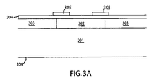
図3Aを参照すると、太陽電池は、ウェハ301並びに複数の拡散領域303及び302の形態の基板を有している。拡散領域303及び302は、ウェハ301又はその上に重ねられた層に形成することができる。図3の例では、拡散領域303はP型拡散領域を含み、拡散領域302はN型拡散領域を含む。本発明の態様による任意の所与の太陽電池ウェハには、いくつかの拡散領域303及び302がある。図3Aの太陽電池は、拡散領域303及び302が、前面304とは反対の側の背面にある背面接合型太陽電池である。前面304は、通常の運転時には太陽の方を向く。
Referring to FIG. 3A, the solar cell has a substrate in the form of a
拡散領域の上には誘電層304が形成されている。一態様では、誘電層304は、大気圧化学蒸着(APCVD)によって約1000〜6000Åの厚みに形成された二酸化シリコンを含む。層304は、拡散領域と、その上に重ねられた導電層、例えば続いて形成される金属コンタクトフィンガーとの間の電気的絶縁をもたらす。
A
誘電層304上には誘電層305が形成されており、これにより、有利には、1つの極性の金属コンタクトフィンガーが別の極性の拡散領域に対して電気的に短絡することが防止される。図3の例では、層305は、N型拡散領域302(つまりN型金属コンタクトフィンガー)に電気的に接続されている金属コンタクトフィンガーがP型拡散領域303に対して電気的に短絡することを防止する。一態様では、誘電層305は、5ミクロンの厚みにスクリーン印刷されたポリイミドを含む。誘電層305は、他の堆積技術を使用して形成することもできる。
A
しかし、誘電層305は、好ましくは、費用を抑えるためにスクリーン印刷されている。費用の低減は、太陽電池用途では特に重要である。一態様では、層305間の開口は約200μmである。
However, the
図3Bでは、複数のドット306が、ウェハ301上にインクジェット印刷されている。認識されるように、ドット306という名称は、ノズルを通る吐出材料によって形成されていることを示すために付けられている。つまり、ドット306は必ずしも円形でなくてよい。ドット306は、ギャップ321がドット306間に形成されるように、ウェハ301上にインクジェット印刷することができる。以下の説明でより明確となるが、ギャップ321はコンタクト領域を画定し、このコンタクト領域を通して、金属コンタクトフィンガーを、対応する拡散領域に電気的に接続することができる。ドット306は、ウェハ301上でのプリントヘッドの1回のパスで形成することができ、それにより、層305間の開口に形成されたギャップ321が得られる。図4のコンタクトマスク400を形成するドット306は、ホットメルト樹脂を含んでいてよい。
In FIG. 3B, a plurality of
図4に、本発明の態様による、ギャップ321と隣接するドット306との位置関係を図示する上面図を示す。図4の例では、コンタクトマスク400は、ギャップ321が形成されるようにインクジェット印刷された複数の重ねられたドット306を含む。ギャップ321は、ドット306が印刷されていないエリアである。図4に示すように、各ギャップ321は、複数の(例えば4つの)重ねられたドット306の交差部によって形成されていてよい。有利には、ギャップ321のサイズ及び位置は、ドット306を供給するノズルの物理的な整列によって規定し、決定することができる。例えば、ドット306の中心間の寸法401は、インクジェットノズルのピッチによって規定することができる。したがって、ギャップ間の間隔も、ドットを供給するノズルの物理的な整列によって決定される。
FIG. 4 shows a top view illustrating the positional relationship between
コンタクトマスク400は、これまで実現されていなかったいくつかの利点を提供する。ドット306間の間隔の精度が、ノズルの物理的な整列によって決定されるので、比較的低いDPIのインクジェットプリンタを、複数のギャップ321を画定するために使用することができる。例えば、+/−5μmで約100μmのドット直径である場合、ドットの中心間の距離401は75μmの長さを有し、各ギャップ321は約6μmの直径を有し得る。好ましくは、各ギャップのサイズは、ギャップが層305中のピンホールと整列する範囲、ひいては確率ができるだけ小さくなるように形成される。同様の理由で、ギャップ321は、好ましくは、層305間の開口内にのみ形成されている。
コンタクトマスク400は、臨界的な整合なしでウェハ301上に印刷することができるという意味で、「整合不要(alignment free)」でもある。その理由は、ギャップ321が層305間の特定の位置で形成される必要がないからであり、つまり、ギャップ321が層305間に形成されてさえいればよい。また、コンタクトマスク400を印刷するために、インクジェットプリンタは、図2のコンタクトマスク200のように複雑なパターンを作る必要はなく、ウェハ301上を単に通過させるだけでよい。コンタクトマスク400は、比較的真っ直ぐな経路に沿って1回又は複数回のパスで印刷することができる。一態様では、コンタクトマスク400は、一方向で1回のパスでインクジェット印刷される。
図3Cへと続き、層304の部分を除去してその層304を貫通するコンタクト領域311を形成するために、コンタクトマスク400が利用される。一態様では、コンタクト領域311は、エッチングマスクとしてコンタクトマスク400を使用し且つ層305をあまり顕著にエッチングをしないエッチャントによって層304をエッチングすることによって形成される。例えば、二酸化シリコンを含む層304及びポリイミドを含む層305の場合は、コンタクト領域311は、エッチャントとしてフッ化水素酸を使用する緩衝酸化物エッチング(BOE)プロセスで、層304の露出した部分(つまりギャップ321の直下の部分)を湿式エッチングすることによって形成することができる。層305は、そのようなエッチングプロセスにおいて、エッチ停止層として働く。図3Cに、BOEプロセス及びそれに続くコンタクトマスク400の除去後の図3Bのサンプルを示す。ホットメルト樹脂を含むコンタクトマスク400は、水酸化カリウム(KOH)を使用するマスクストリッププロセスで除去することができる。
Continuing to FIG. 3C,
図3Cに示すように、コンタクトマスク400によって、層305間の開口において複数のコンタクト領域311が得られた。コンタクト領域311は、コンタクト領域311を画定するのに使用される対応ギャップ321のサイズが小さいため、比較的小さい。よって、対応する拡散領域との電気的な接続を金属コンタクトフィンガーが貫通して形成することができる複数の比較的小さいコンタクト領域311が得られる。コンタクト領域311のサイズが比較的小さい(例えば、同じサイズのギャップ321に対し6μm)ことによって、比較的小さな金属コンタクトフィンガーの利用が可能となり、そしてそれにより、有利には、より高い効率が得られる。
As shown in FIG. 3C, the
図3Dでは、金属コンタクトフィンガー312及び313が、コンタクト領域311を貫通して形成されている。一態様では、金属コンタクトフィンガー312及び313は材料の積層体を含む。その材料は、1000オングストロームの厚みのアルミニウム層を含み、そのアルミニウム層は500オングストロームのチタン−タングステン層上に形成されていて、そのチタン−タングステン層は300ミクロンの厚みの銅層上に形成され、その銅層は6ミクロンの厚みのスズ層上に形成されている。本発明の利点を損なうことがなければ、別の金属及び金属構造も使用することができる。本発明の態様による任意の所与の太陽電池ウェハでは、いくつかの金属コンタクトフィンガー312及び313が設けられている。図3Dの例では、金属コンタクトフィンガー312は、コンタクト領域311を通ってP型拡散領域303に電気的に接続されており、P型の金属コンタクトフィンガーである。同様に、金属コンタクトフィンガー313は、コンタクト領域311を通ってN型拡散領域302に電気的に接続されており、N型金属コンタクトフィンガーである。外部電気回路を金属コンタクトフィンガーに接続させ、これにより、太陽電池から電力を受け取ることができる。
In FIG. 3D,
図4に示すドット306は、ウェハ上でのプリントヘッドの1回のパスで印刷することができる。ウェハ上での2つ以上のパスを実施し、例えば特定のギャップ321を覆うこともできる。図5の例では、プリントヘッドの第1のパスが、図4に示すようにコンタクトマスク400を形成し、プリントヘッドの第2のパスが、ギャップ321が(ドット306Aの下で)覆われるようにドット306Aを形成する。
The
新規の太陽電池製造のための小さなコンタクトのアレイを開示する。特定の本発明の態様を示したが、これらの態様が例示を目的としており、限定のためのものでないことを理解されたい。本開示を読むことで、多数の追加的な態様が当業者に明らかとなろう。 An array of small contacts for novel solar cell manufacturing is disclosed. While particular embodiments of the present invention have been shown, it is to be understood that these embodiments are for purposes of illustration and are not intended to be limiting. Many additional aspects will become apparent to those of ordinary skill in the art upon reading this disclosure.
Claims (10)
前記第1の誘電層上に複数の第2の誘電層を形成し、
前記複数の第2の誘電層間の少なくとも複数の開口に、複数のドットをインクジェット印刷し、前記複数のドットの交差部によって形成された当該複数のドットよりも小さな領域を有する複数のギャップを形成し、該ギャップのサイズが、少なくとも(i)前記複数のドットを供給する複数のインクジェットプリンタノズルの整列と、(ii)前記複数のドットのサイズと、(iii)いずれのノズルを使用したか、によって決定される、太陽電池の製造方法。 Forming a first dielectric layer on a wafer to be processed into a solar cell;
Forming a plurality of second dielectric layers on the first dielectric layer;
A plurality of dots are inkjet printed in at least a plurality of openings between the plurality of second dielectric layers to form a plurality of gaps having regions smaller than the plurality of dots formed by intersections of the plurality of dots. The size of the gap depends on at least (i) the alignment of a plurality of inkjet printer nozzles that supply the plurality of dots , (ii) the size of the plurality of dots, and (iii) which nozzle was used . The manufacturing method of the solar cell determined.
前記ウェハから前記複数のドットを除去し、
前記第1の誘電層の上に複数の金属コンタクトフィンガーを形成し、前記複数のコンタクト領域を通して、前記第1の誘電層の下に設けられている複数の拡散領域との複数の電気的な接続を形成する
ことをさらに含む、請求項1に記載の太陽電池の製造方法。 Using the plurality of dots as a mask to form a plurality of contact regions penetrating the first dielectric layer;
Removing the plurality of dots from the wafer;
Said first dielectric layer a plurality of metallic contact fingers is formed on, through the plurality of contact regions, the plurality of electrical connection between the plurality of diffusion regions are provided below the first dielectric layer The method for manufacturing a solar cell according to claim 1, further comprising: forming.
前記複数のP型拡散領域及び前記複数のN型拡散領域が、前記ウェハの、通常の運転時に太陽の方を向くウェハの前面とは反対側の背面に形成されている、請求項3に記載の太陽電池の製造方法。 A plurality of at least some of said plurality of metal contact fingers, through at least some of said plurality of contact regions, formed to produce a plurality of electrical connection between the corresponding plurality of N-type diffusion region A plurality of P-type metals formed to produce a plurality of electrical connections between a plurality of N-type metal contact fingers and a corresponding plurality of P-type diffusion regions through at least some of the plurality of contact regions Including contact fingers,
The plurality of P-type diffusion regions and the plurality of N-type diffusion regions are formed on a back surface of the wafer opposite to the front surface of the wafer facing the sun during normal operation. Solar cell manufacturing method.
前記第1の誘電層上であって、一対の隣接する前記複数の拡散領域の境界の上に複数の第2の誘電層を形成し、
前記複数の第2の誘電層のうちの少なくとも2つの誘電層の間の開口に、複数のドットを印刷し、前記複数のドットが、当該複数のドットよりも小さな領域を有する複数のギャップを形成するコンタクトマスクを形成し、前記複数のギャップのそれぞれが、前記複数のドットにおいて重ねられた複数のドットの交差部によって画定され、
前記第1の誘電層の、前記複数のギャップを通って露出している複数の部分をエッチングし、複数のコンタクト領域を形成して、前記太陽電池の前記複数の拡散領域を露出させることを含む、太陽電池の製造方法。 Forming a first dielectric layer on a solar cell wafer having a plurality of diffusion regions adjacent to each other;
A first dielectric layer, forming a second dielectric layer a plurality of on the border of the plurality of diffusion regions adjacent pair of,
The opening between the at least two Yuden layer of the plurality of second dielectric layer, and printing a plurality of dots, the plurality of dots, a plurality of gaps having a smaller area than the plurality of dots Each of the plurality of gaps is defined by an intersection of a plurality of dots overlaid on the plurality of dots,
Of the first dielectric layer, etching the plurality of portions which are exposed through said plurality of gaps, and forming a plurality of contact regions, and exposing the plurality of diffusion regions of the solar cell The manufacturing method of a solar cell.
前記複数のコンタクト領域内に複数の金属コンタクトフィンガーを形成し、前記複数の拡散領域のうち対応するものに電気的に接続すること
をさらに含む、請求項8に記載の太陽電池の製造方法。 Removing the plurality of dots from the wafer;
The method for manufacturing a solar cell according to claim 8, further comprising forming a plurality of metal contact fingers in the plurality of contact regions and electrically connecting to a corresponding one of the plurality of diffusion regions.
Applications Claiming Priority (3)
| Application Number | Priority Date | Filing Date | Title |
|---|---|---|---|
| US11/807,567 | 2007-05-29 | ||
| US11/807,567 US7838062B2 (en) | 2007-05-29 | 2007-05-29 | Array of small contacts for solar cell fabrication |
| PCT/US2008/006017 WO2008150344A1 (en) | 2007-05-29 | 2008-05-12 | Array of small contacts for solar cell fabrication |
Related Child Applications (1)
| Application Number | Title | Priority Date | Filing Date |
|---|---|---|---|
| JP2014080282A Division JP5767359B2 (en) | 2007-05-29 | 2014-04-09 | Manufacturing method of solar cell |
Publications (3)
| Publication Number | Publication Date |
|---|---|
| JP2010528487A JP2010528487A (en) | 2010-08-19 |
| JP2010528487A5 JP2010528487A5 (en) | 2011-06-30 |
| JP5791896B2 true JP5791896B2 (en) | 2015-10-07 |
Family
ID=40088567
Family Applications (2)
| Application Number | Title | Priority Date | Filing Date |
|---|---|---|---|
| JP2010510284A Expired - Fee Related JP5791896B2 (en) | 2007-05-29 | 2008-05-12 | Array of small contacts for solar cell manufacturing |
| JP2014080282A Expired - Fee Related JP5767359B2 (en) | 2007-05-29 | 2014-04-09 | Manufacturing method of solar cell |
Family Applications After (1)
| Application Number | Title | Priority Date | Filing Date |
|---|---|---|---|
| JP2014080282A Expired - Fee Related JP5767359B2 (en) | 2007-05-29 | 2014-04-09 | Manufacturing method of solar cell |
Country Status (7)
| Country | Link |
|---|---|
| US (2) | US7838062B2 (en) |
| EP (1) | EP2153466B1 (en) |
| JP (2) | JP5791896B2 (en) |
| KR (1) | KR101384498B1 (en) |
| CN (1) | CN101681902B (en) |
| AU (1) | AU2008260627B2 (en) |
| WO (1) | WO2008150344A1 (en) |
Families Citing this family (29)
| Publication number | Priority date | Publication date | Assignee | Title |
|---|---|---|---|---|
| US8853527B2 (en) | 2007-02-16 | 2014-10-07 | Nanogram Corporation | Solar cell structures, photovoltaic panels and corresponding processes |
| US7838062B2 (en) * | 2007-05-29 | 2010-11-23 | Sunpower Corporation | Array of small contacts for solar cell fabrication |
| US20100294349A1 (en) * | 2009-05-20 | 2010-11-25 | Uma Srinivasan | Back contact solar cells with effective and efficient designs and corresponding patterning processes |
| US8211731B2 (en) | 2010-06-07 | 2012-07-03 | Sunpower Corporation | Ablation of film stacks in solar cell fabrication processes |
| US8263899B2 (en) | 2010-07-01 | 2012-09-11 | Sunpower Corporation | High throughput solar cell ablation system |
| US8912083B2 (en) | 2011-01-31 | 2014-12-16 | Nanogram Corporation | Silicon substrates with doped surface contacts formed from doped silicon inks and corresponding processes |
| US8586403B2 (en) | 2011-02-15 | 2013-11-19 | Sunpower Corporation | Process and structures for fabrication of solar cells with laser ablation steps to form contact holes |
| US8692111B2 (en) | 2011-08-23 | 2014-04-08 | Sunpower Corporation | High throughput laser ablation processes and structures for forming contact holes in solar cells |
| US8822262B2 (en) | 2011-12-22 | 2014-09-02 | Sunpower Corporation | Fabricating solar cells with silicon nanoparticles |
| US8513045B1 (en) | 2012-01-31 | 2013-08-20 | Sunpower Corporation | Laser system with multiple laser pulses for fabrication of solar cells |
| FR2995451B1 (en) * | 2012-09-11 | 2014-10-24 | Commissariat Energie Atomique | METHOD FOR METALLIZING A PHOTOVOLTAIC CELL AND PHOTOVOLTAIC CELL THUS OBTAINED |
| US9577134B2 (en) * | 2013-12-09 | 2017-02-21 | Sunpower Corporation | Solar cell emitter region fabrication using self-aligned implant and cap |
| US9337369B2 (en) | 2014-03-28 | 2016-05-10 | Sunpower Corporation | Solar cells with tunnel dielectrics |
| US9911874B2 (en) * | 2014-05-30 | 2018-03-06 | Sunpower Corporation | Alignment free solar cell metallization |
| US9559219B1 (en) * | 2014-06-23 | 2017-01-31 | Sandia Corporation | Fast process flow, on-wafer interconnection and singulation for MEPV |
| US10840394B2 (en) * | 2015-09-25 | 2020-11-17 | Total Marketing Services | Conductive strip based mask for metallization of semiconductor devices |
| USD822890S1 (en) | 2016-09-07 | 2018-07-10 | Felxtronics Ap, Llc | Lighting apparatus |
| US10775030B2 (en) | 2017-05-05 | 2020-09-15 | Flex Ltd. | Light fixture device including rotatable light modules |
| USD832494S1 (en) | 2017-08-09 | 2018-10-30 | Flex Ltd. | Lighting module heatsink |
| USD862777S1 (en) | 2017-08-09 | 2019-10-08 | Flex Ltd. | Lighting module wide distribution lens |
| USD846793S1 (en) | 2017-08-09 | 2019-04-23 | Flex Ltd. | Lighting module locking mechanism |
| USD833061S1 (en) | 2017-08-09 | 2018-11-06 | Flex Ltd. | Lighting module locking endcap |
| USD877964S1 (en) | 2017-08-09 | 2020-03-10 | Flex Ltd. | Lighting module |
| USD872319S1 (en) | 2017-08-09 | 2020-01-07 | Flex Ltd. | Lighting module LED light board |
| USD832495S1 (en) | 2017-08-18 | 2018-10-30 | Flex Ltd. | Lighting module locking mechanism |
| USD862778S1 (en) | 2017-08-22 | 2019-10-08 | Flex Ltd | Lighting module lens |
| USD888323S1 (en) | 2017-09-07 | 2020-06-23 | Flex Ltd | Lighting module wire guard |
| JP6875252B2 (en) | 2017-10-26 | 2021-05-19 | 信越化学工業株式会社 | Method of drying polyimide paste and method of manufacturing high photoelectric conversion efficiency solar cell |
| DE102021106232A1 (en) * | 2021-03-15 | 2022-09-15 | Airbus Operations Gmbh | Painting method with printed mask and printing device |
Family Cites Families (47)
| Publication number | Priority date | Publication date | Assignee | Title |
|---|---|---|---|---|
| US4234352A (en) * | 1978-07-26 | 1980-11-18 | Electric Power Research Institute, Inc. | Thermophotovoltaic converter and cell for use therein |
| EP0018924B2 (en) * | 1979-05-08 | 1989-01-04 | Saint Gobain Vitrage International | Method of manufacturing solar-cell panels and panels obtained by this method |
| US4429657A (en) * | 1979-12-13 | 1984-02-07 | Additive Technology Corporation | Method, materials and apparatus for manufacturing printed circuits |
| US4387116A (en) * | 1981-12-28 | 1983-06-07 | Exxon Research And Engineering Co. | Conditioner for adherence of nickel to a tin oxide surface |
| US4478879A (en) * | 1983-02-10 | 1984-10-23 | The United States Of America As Represented By The Administrator Of The National Aeronautics And Space Administration | Screen printed interdigitated back contact solar cell |
| US4838952A (en) * | 1988-04-29 | 1989-06-13 | Spectrolab, Inc. | Controlled reflectance solar cell |
| US4927770A (en) * | 1988-11-14 | 1990-05-22 | Electric Power Research Inst. Corp. Of District Of Columbia | Method of fabricating back surface point contact solar cells |
| US5217539A (en) * | 1991-09-05 | 1993-06-08 | The Boeing Company | III-V solar cells and doping processes |
| US5053083A (en) * | 1989-05-08 | 1991-10-01 | The Board Of Trustees Of The Leland Stanford Junior University | Bilevel contact solar cells |
| US5164019A (en) * | 1991-07-31 | 1992-11-17 | Sunpower Corporation | Monolithic series-connected solar cells having improved cell isolation and method of making same |
| US5185042A (en) * | 1991-08-01 | 1993-02-09 | Trw Inc. | Generic solar cell array using a printed circuit substrate |
| US5360990A (en) * | 1993-03-29 | 1994-11-01 | Sunpower Corporation | P/N junction device having porous emitter |
| US5369291A (en) * | 1993-03-29 | 1994-11-29 | Sunpower Corporation | Voltage controlled thyristor |
| US5468652A (en) * | 1993-07-14 | 1995-11-21 | Sandia Corporation | Method of making a back contacted solar cell |
| EP0645444A3 (en) * | 1993-09-27 | 1995-05-24 | Texaco Development Corp | Lubricants with linear alkaryl overbased detergents. |
| EP0840381A3 (en) * | 1996-10-31 | 1999-08-04 | Sony Corporation | Thin-film semiconductor device and its manufacturing method and apparatus and thin-film semiconductor solar cell module and its manufacturing method |
| JP3639703B2 (en) | 1997-11-14 | 2005-04-20 | キヤノン株式会社 | Inkjet recording apparatus and inkjet recording method |
| US5972732A (en) | 1997-12-19 | 1999-10-26 | Sandia Corporation | Method of monolithic module assembly |
| US6278054B1 (en) * | 1998-05-28 | 2001-08-21 | Tecstar Power Systems, Inc. | Solar cell having an integral monolithically grown bypass diode |
| US6337283B1 (en) * | 1999-12-30 | 2002-01-08 | Sunpower Corporation | Method of fabricating a silicon solar cell |
| US6274402B1 (en) * | 1999-12-30 | 2001-08-14 | Sunpower Corporation | Method of fabricating a silicon solar cell |
| US6423568B1 (en) * | 1999-12-30 | 2002-07-23 | Sunpower Corporation | Method of fabricating a silicon solar cell |
| US6387726B1 (en) * | 1999-12-30 | 2002-05-14 | Sunpower Corporation | Method of fabricating a silicon solar cell |
| US6313395B1 (en) * | 2000-04-24 | 2001-11-06 | Sunpower Corporation | Interconnect structure for solar cells and method of making same |
| JP3968554B2 (en) * | 2000-05-01 | 2007-08-29 | セイコーエプソン株式会社 | Bump forming method and semiconductor device manufacturing method |
| US6333457B1 (en) * | 2000-08-29 | 2001-12-25 | Sunpower Corporation | Edge passivated silicon solar/photo cell and method of manufacture |
| GB2367788A (en) * | 2000-10-16 | 2002-04-17 | Seiko Epson Corp | Etching using an ink jet print head |
| JP4137415B2 (en) * | 2000-11-21 | 2008-08-20 | シャープ株式会社 | How to replace solar cells |
| DE10139441C1 (en) * | 2001-08-10 | 2002-10-10 | Astrium Gmbh | Method for repairing solar panels comprises placing protective sheet over intact arrays, replacement array then being glued over defective array and welded connections made to intact arrays |
| JP2003298078A (en) | 2002-03-29 | 2003-10-17 | Ebara Corp | Photoelectromotive element |
| US6872321B2 (en) * | 2002-09-25 | 2005-03-29 | Lsi Logic Corporation | Direct positive image photo-resist transfer of substrate design |
| JP2004134499A (en) * | 2002-10-09 | 2004-04-30 | Sharp Corp | Process and system for producing solar cell |
| JP2004209887A (en) * | 2003-01-07 | 2004-07-29 | Seiko Epson Corp | Liquid discharge device, liquid discharge method, program and computer system |
| JPWO2004070823A1 (en) * | 2003-02-05 | 2006-06-01 | 株式会社半導体エネルギー研究所 | Method for manufacturing display device |
| US7388147B2 (en) * | 2003-04-10 | 2008-06-17 | Sunpower Corporation | Metal contact structure for solar cell and method of manufacture |
| JP4344270B2 (en) * | 2003-05-30 | 2009-10-14 | セイコーエプソン株式会社 | Manufacturing method of liquid crystal display device |
| US6998288B1 (en) * | 2003-10-03 | 2006-02-14 | Sunpower Corporation | Use of doped silicon dioxide in the fabrication of solar cells |
| JP2006073617A (en) * | 2004-08-31 | 2006-03-16 | Sharp Corp | Solar cell and manufacturing method thereof |
| JP4605361B2 (en) * | 2004-10-29 | 2011-01-05 | 独立行政法人科学技術振興機構 | Foil and manufacturing method thereof |
| JP2006156542A (en) * | 2004-11-26 | 2006-06-15 | Seiko Epson Corp | Method for forming resist pattern using ink jet system, method for manufacturing surface acoustic wave element piece, and surface acoustic wave device |
| JP5000119B2 (en) * | 2005-02-17 | 2012-08-15 | Jx日鉱日石エネルギー株式会社 | Dye-sensitized solar cell element |
| US7554031B2 (en) * | 2005-03-03 | 2009-06-30 | Sunpower Corporation | Preventing harmful polarization of solar cells |
| JP4656996B2 (en) * | 2005-04-21 | 2011-03-23 | シャープ株式会社 | Solar cell |
| JP2007125855A (en) * | 2005-11-07 | 2007-05-24 | Sony Corp | Image forming method |
| US20070295399A1 (en) * | 2005-12-16 | 2007-12-27 | Bp Corporation North America Inc. | Back-Contact Photovoltaic Cells |
| US7838062B2 (en) * | 2007-05-29 | 2010-11-23 | Sunpower Corporation | Array of small contacts for solar cell fabrication |
| US8274402B1 (en) | 2008-01-24 | 2012-09-25 | LDARtools, Inc. | Data collection process for optical leak detection |
-
2007
- 2007-05-29 US US11/807,567 patent/US7838062B2/en active Active
-
2008
- 2008-05-12 CN CN2008800161241A patent/CN101681902B/en active Active
- 2008-05-12 JP JP2010510284A patent/JP5791896B2/en not_active Expired - Fee Related
- 2008-05-12 WO PCT/US2008/006017 patent/WO2008150344A1/en active Application Filing
- 2008-05-12 KR KR1020097024837A patent/KR101384498B1/en active IP Right Grant
- 2008-05-12 EP EP08754346.8A patent/EP2153466B1/en not_active Not-in-force
- 2008-05-12 AU AU2008260627A patent/AU2008260627B2/en active Active
-
2010
- 2010-11-18 US US12/949,523 patent/US8883247B2/en active Active
-
2014
- 2014-04-09 JP JP2014080282A patent/JP5767359B2/en not_active Expired - Fee Related
Also Published As
| Publication number | Publication date |
|---|---|
| AU2008260627B2 (en) | 2013-08-15 |
| EP2153466A4 (en) | 2014-04-09 |
| EP2153466B1 (en) | 2015-10-21 |
| CN101681902B (en) | 2012-07-04 |
| US8883247B2 (en) | 2014-11-11 |
| JP2014168076A (en) | 2014-09-11 |
| CN101681902A (en) | 2010-03-24 |
| WO2008150344A1 (en) | 2008-12-11 |
| US20080299297A1 (en) | 2008-12-04 |
| EP2153466A1 (en) | 2010-02-17 |
| US7838062B2 (en) | 2010-11-23 |
| AU2008260627A1 (en) | 2008-12-11 |
| KR20100017457A (en) | 2010-02-16 |
| KR101384498B1 (en) | 2014-04-14 |
| JP5767359B2 (en) | 2015-08-19 |
| US20110061731A1 (en) | 2011-03-17 |
| JP2010528487A (en) | 2010-08-19 |
Similar Documents
| Publication | Publication Date | Title |
|---|---|---|
| JP5791896B2 (en) | Array of small contacts for solar cell manufacturing | |
| JP2010528487A5 (en) | ||
| JP6091587B2 (en) | Fine line metallization of photovoltaic devices by partial lift-off of optical coatings | |
| JP4656996B2 (en) | Solar cell | |
| KR20210046826A (en) | Hybrid emitter all back contact solar cell | |
| JP4944240B1 (en) | Back electrode type solar cell, back electrode type solar cell with wiring sheet, solar cell module, method for manufacturing back electrode type solar cell with wiring sheet, and method for manufacturing solar cell module | |
| JP5046819B2 (en) | Through-hole forming method and inkjet head | |
| JP4217434B2 (en) | Through-hole forming method and inkjet head using the same | |
| US8927424B1 (en) | Self-aligned patterning technique for semiconductor device features | |
| CN114103477A (en) | Thermal head, method of manufacturing thermal head, and thermal printer | |
| EP3382892B1 (en) | Method of processing inconsistencies in solar cell devices and devices formed thereby | |
| US7204020B2 (en) | Method for fabricating a charge plate for an inkjet printhead | |
| US10052870B2 (en) | Liquid supply substrate, method of producing the same, and liquid ejecting head | |
| US8104170B2 (en) | Charge plate fabrication technique | |
| JP5274694B2 (en) | Through-hole forming method, inkjet head, and silicon substrate | |
| JP2016171095A (en) | Solar cell and method for manufacturing solar cell | |
| JP2001310474A (en) | Electrostatic actuator, production method therefor, imaging head, and imaging device |
Legal Events
| Date | Code | Title | Description |
|---|---|---|---|
| RD02 | Notification of acceptance of power of attorney |
Free format text: JAPANESE INTERMEDIATE CODE: A7422 Effective date: 20100727 |
|
| RD04 | Notification of resignation of power of attorney |
Free format text: JAPANESE INTERMEDIATE CODE: A7424 Effective date: 20100803 |
|
| A521 | Request for written amendment filed |
Free format text: JAPANESE INTERMEDIATE CODE: A821 Effective date: 20100803 |
|
| A072 | Dismissal of procedure [no reply to invitation to correct request for examination] |
Free format text: JAPANESE INTERMEDIATE CODE: A073 Effective date: 20110329 |
|
| A521 | Request for written amendment filed |
Free format text: JAPANESE INTERMEDIATE CODE: A523 Effective date: 20110509 |
|
| A621 | Written request for application examination |
Free format text: JAPANESE INTERMEDIATE CODE: A621 Effective date: 20110509 |
|
| A072 | Dismissal of procedure [no reply to invitation to correct request for examination] |
Free format text: JAPANESE INTERMEDIATE CODE: A073 Effective date: 20110712 |
|
| A977 | Report on retrieval |
Free format text: JAPANESE INTERMEDIATE CODE: A971007 Effective date: 20121228 |
|
| A131 | Notification of reasons for refusal |
Free format text: JAPANESE INTERMEDIATE CODE: A131 Effective date: 20130108 |
|
| A521 | Request for written amendment filed |
Free format text: JAPANESE INTERMEDIATE CODE: A523 Effective date: 20130408 |
|
| A131 | Notification of reasons for refusal |
Free format text: JAPANESE INTERMEDIATE CODE: A131 Effective date: 20130723 |
|
| A521 | Request for written amendment filed |
Free format text: JAPANESE INTERMEDIATE CODE: A523 Effective date: 20131016 |
|
| A02 | Decision of refusal |
Free format text: JAPANESE INTERMEDIATE CODE: A02 Effective date: 20131210 |
|
| A521 | Request for written amendment filed |
Free format text: JAPANESE INTERMEDIATE CODE: A523 Effective date: 20140409 |
|
| A911 | Transfer to examiner for re-examination before appeal (zenchi) |
Free format text: JAPANESE INTERMEDIATE CODE: A911 Effective date: 20140421 |
|
| A912 | Re-examination (zenchi) completed and case transferred to appeal board |
Free format text: JAPANESE INTERMEDIATE CODE: A912 Effective date: 20140627 |
|
| A61 | First payment of annual fees (during grant procedure) |
Free format text: JAPANESE INTERMEDIATE CODE: A61 Effective date: 20150805 |
|
| R150 | Certificate of patent or registration of utility model |
Ref document number: 5791896 Country of ref document: JP Free format text: JAPANESE INTERMEDIATE CODE: R150 |
|
| LAPS | Cancellation because of no payment of annual fees |