US4387116A - Conditioner for adherence of nickel to a tin oxide surface - Google Patents
Conditioner for adherence of nickel to a tin oxide surface Download PDFInfo
- Publication number
- US4387116A US4387116A US06/335,229 US33522981A US4387116A US 4387116 A US4387116 A US 4387116A US 33522981 A US33522981 A US 33522981A US 4387116 A US4387116 A US 4387116A
- Authority
- US
- United States
- Prior art keywords
- tin
- oxide surface
- layer
- nickel
- amount
- Prior art date
- Legal status (The legal status is an assumption and is not a legal conclusion. Google has not performed a legal analysis and makes no representation as to the accuracy of the status listed.)
- Expired - Fee Related
Links
- PXHVJJICTQNCMI-UHFFFAOYSA-N Nickel Chemical compound [Ni] PXHVJJICTQNCMI-UHFFFAOYSA-N 0.000 title claims abstract description 48
- XOLBLPGZBRYERU-UHFFFAOYSA-N tin dioxide Chemical compound O=[Sn]=O XOLBLPGZBRYERU-UHFFFAOYSA-N 0.000 title claims abstract description 30
- 229910001887 tin oxide Inorganic materials 0.000 title claims abstract description 30
- 229910052759 nickel Inorganic materials 0.000 title claims abstract description 24
- 238000000034 method Methods 0.000 claims abstract description 11
- KRHYYFGTRYWZRS-UHFFFAOYSA-N Fluorane Chemical compound F KRHYYFGTRYWZRS-UHFFFAOYSA-N 0.000 claims description 16
- VEXZGXHMUGYJMC-UHFFFAOYSA-N Hydrochloric acid Chemical compound Cl VEXZGXHMUGYJMC-UHFFFAOYSA-N 0.000 claims description 10
- 239000011248 coating agent Substances 0.000 claims description 10
- 238000000576 coating method Methods 0.000 claims description 10
- HPGGPRDJHPYFRM-UHFFFAOYSA-J tin(iv) chloride Chemical compound Cl[Sn](Cl)(Cl)Cl HPGGPRDJHPYFRM-UHFFFAOYSA-J 0.000 claims description 8
- XLYOFNOQVPJJNP-UHFFFAOYSA-N water Substances O XLYOFNOQVPJJNP-UHFFFAOYSA-N 0.000 claims description 7
- 230000000873 masking effect Effects 0.000 claims description 6
- 238000007747 plating Methods 0.000 claims description 6
- VYPSYNLAJGMNEJ-UHFFFAOYSA-N Silicium dioxide Chemical compound O=[Si]=O VYPSYNLAJGMNEJ-UHFFFAOYSA-N 0.000 claims description 5
- 238000005530 etching Methods 0.000 claims description 5
- 239000000463 material Substances 0.000 claims description 5
- 230000001143 conditioned effect Effects 0.000 claims description 4
- 229910052814 silicon oxide Inorganic materials 0.000 claims description 3
- LFQSCWFLJHTTHZ-UHFFFAOYSA-N Ethanol Chemical compound CCO LFQSCWFLJHTTHZ-UHFFFAOYSA-N 0.000 claims 1
- 230000001235 sensitizing effect Effects 0.000 claims 1
- 210000004027 cell Anatomy 0.000 description 17
- 229910000679 solder Inorganic materials 0.000 description 4
- 239000000758 substrate Substances 0.000 description 4
- XUIMIQQOPSSXEZ-UHFFFAOYSA-N Silicon Chemical compound [Si] XUIMIQQOPSSXEZ-UHFFFAOYSA-N 0.000 description 3
- 239000007788 liquid Substances 0.000 description 3
- 239000000203 mixture Substances 0.000 description 3
- 229910052710 silicon Inorganic materials 0.000 description 3
- 239000010703 silicon Substances 0.000 description 3
- KDLHZDBZIXYQEI-UHFFFAOYSA-N Palladium Chemical compound [Pd] KDLHZDBZIXYQEI-UHFFFAOYSA-N 0.000 description 2
- 230000015572 biosynthetic process Effects 0.000 description 2
- 230000008021 deposition Effects 0.000 description 2
- 230000004907 flux Effects 0.000 description 2
- DOVLZBWRSUUIJA-UHFFFAOYSA-N oxotin;silicon Chemical compound [Si].[Sn]=O DOVLZBWRSUUIJA-UHFFFAOYSA-N 0.000 description 2
- 238000002360 preparation method Methods 0.000 description 2
- 238000009987 spinning Methods 0.000 description 2
- 239000002253 acid Substances 0.000 description 1
- 239000005456 alcohol based solvent Substances 0.000 description 1
- 239000010426 asphalt Substances 0.000 description 1
- 230000005540 biological transmission Effects 0.000 description 1
- 239000003795 chemical substances by application Substances 0.000 description 1
- 229910052681 coesite Inorganic materials 0.000 description 1
- 229910052906 cristobalite Inorganic materials 0.000 description 1
- 238000009792 diffusion process Methods 0.000 description 1
- 238000007598 dipping method Methods 0.000 description 1
- 238000009713 electroplating Methods 0.000 description 1
- 230000008020 evaporation Effects 0.000 description 1
- 238000001704 evaporation Methods 0.000 description 1
- FDWREHZXQUYJFJ-UHFFFAOYSA-M gold monochloride Chemical compound [Cl-].[Au+] FDWREHZXQUYJFJ-UHFFFAOYSA-M 0.000 description 1
- 238000004519 manufacturing process Methods 0.000 description 1
- 229910052751 metal Inorganic materials 0.000 description 1
- 239000002184 metal Substances 0.000 description 1
- 238000002156 mixing Methods 0.000 description 1
- 230000003287 optical effect Effects 0.000 description 1
- 229910052763 palladium Inorganic materials 0.000 description 1
- 239000002244 precipitate Substances 0.000 description 1
- 230000005855 radiation Effects 0.000 description 1
- 230000001105 regulatory effect Effects 0.000 description 1
- 239000000377 silicon dioxide Substances 0.000 description 1
- 238000005476 soldering Methods 0.000 description 1
- 239000002904 solvent Substances 0.000 description 1
- 238000003892 spreading Methods 0.000 description 1
- 229910052682 stishovite Inorganic materials 0.000 description 1
- 239000000126 substance Substances 0.000 description 1
- 230000003319 supportive effect Effects 0.000 description 1
- 229910052905 tridymite Inorganic materials 0.000 description 1
Images
Classifications
-
- C—CHEMISTRY; METALLURGY
- C23—COATING METALLIC MATERIAL; COATING MATERIAL WITH METALLIC MATERIAL; CHEMICAL SURFACE TREATMENT; DIFFUSION TREATMENT OF METALLIC MATERIAL; COATING BY VACUUM EVAPORATION, BY SPUTTERING, BY ION IMPLANTATION OR BY CHEMICAL VAPOUR DEPOSITION, IN GENERAL; INHIBITING CORROSION OF METALLIC MATERIAL OR INCRUSTATION IN GENERAL
- C23C—COATING METALLIC MATERIAL; COATING MATERIAL WITH METALLIC MATERIAL; SURFACE TREATMENT OF METALLIC MATERIAL BY DIFFUSION INTO THE SURFACE, BY CHEMICAL CONVERSION OR SUBSTITUTION; COATING BY VACUUM EVAPORATION, BY SPUTTERING, BY ION IMPLANTATION OR BY CHEMICAL VAPOUR DEPOSITION, IN GENERAL
- C23C18/00—Chemical coating by decomposition of either liquid compounds or solutions of the coating forming compounds, without leaving reaction products of surface material in the coating; Contact plating
- C23C18/16—Chemical coating by decomposition of either liquid compounds or solutions of the coating forming compounds, without leaving reaction products of surface material in the coating; Contact plating by reduction or substitution, e.g. electroless plating
- C23C18/18—Pretreatment of the material to be coated
- C23C18/1851—Pretreatment of the material to be coated of surfaces of non-metallic or semiconducting in organic material
- C23C18/1872—Pretreatment of the material to be coated of surfaces of non-metallic or semiconducting in organic material by chemical pretreatment
- C23C18/1886—Multistep pretreatment
- C23C18/1889—Multistep pretreatment with use of metal first
-
- H—ELECTRICITY
- H01—ELECTRIC ELEMENTS
- H01L—SEMICONDUCTOR DEVICES NOT COVERED BY CLASS H10
- H01L31/00—Semiconductor devices sensitive to infrared radiation, light, electromagnetic radiation of shorter wavelength or corpuscular radiation and specially adapted either for the conversion of the energy of such radiation into electrical energy or for the control of electrical energy by such radiation; Processes or apparatus specially adapted for the manufacture or treatment thereof or of parts thereof; Details thereof
- H01L31/02—Details
- H01L31/0224—Electrodes
- H01L31/022408—Electrodes for devices characterised by at least one potential jump barrier or surface barrier
- H01L31/022425—Electrodes for devices characterised by at least one potential jump barrier or surface barrier for solar cells
-
- H—ELECTRICITY
- H05—ELECTRIC TECHNIQUES NOT OTHERWISE PROVIDED FOR
- H05K—PRINTED CIRCUITS; CASINGS OR CONSTRUCTIONAL DETAILS OF ELECTRIC APPARATUS; MANUFACTURE OF ASSEMBLAGES OF ELECTRICAL COMPONENTS
- H05K3/00—Apparatus or processes for manufacturing printed circuits
- H05K3/22—Secondary treatment of printed circuits
- H05K3/24—Reinforcing the conductive pattern
- H05K3/244—Finish plating of conductors, especially of copper conductors, e.g. for pads or lands
-
- Y—GENERAL TAGGING OF NEW TECHNOLOGICAL DEVELOPMENTS; GENERAL TAGGING OF CROSS-SECTIONAL TECHNOLOGIES SPANNING OVER SEVERAL SECTIONS OF THE IPC; TECHNICAL SUBJECTS COVERED BY FORMER USPC CROSS-REFERENCE ART COLLECTIONS [XRACs] AND DIGESTS
- Y02—TECHNOLOGIES OR APPLICATIONS FOR MITIGATION OR ADAPTATION AGAINST CLIMATE CHANGE
- Y02E—REDUCTION OF GREENHOUSE GAS [GHG] EMISSIONS, RELATED TO ENERGY GENERATION, TRANSMISSION OR DISTRIBUTION
- Y02E10/00—Energy generation through renewable energy sources
- Y02E10/50—Photovoltaic [PV] energy
Definitions
- the present invention relates to the adherence of nickel to any substance with a tin oxide surface.
- optical electronic devices comprising an electrically conducting transparent window material deposited on a semi-conductive substrate.
- Such interest is based on the potential that devices can be fabricated at lower costs than homojunction devices based on the conventional diffusion of N and/or P materials on a surface.
- such devices offer the added advantage that the transparent window permits the transmission of a solar radiation directly to the active substrate with little or no attenuation.
- One such type of material proposed is a tin oxide layer on a conductive substrate.
- the present invention is a solution and a method for its use in adhering nickel to a tin-oxide surface.
- the solution includes:
- the solution is used by immersing the tin-oxide surface into the solution for 30 seconds to 5 minutes at 60°-100° C.
- the treated tin-oxide surface is then sensitized and electrolessly plated with a layer including nickel.
- the solution and method is to apply electroless nickel to a solar cell with a tin-oxide surface.
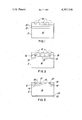
- FIGS. 1 through 3 illustrate cross-sectional views of the solar cell during successive steps in the fabrication technique of a preferred embodiment of the present invention.
- the present invention is a solution and a method for its use in adhering nickel to tin-oxide.
- the solution includes tin chloride.2H 2 O from 30 to 100 gm per liter, hydrochloric (35-38%) acid in an amount of 200 to 400 ml per liter, hydrofluoric acid in an amount 25 to 100 ml per liter, and water making up the remainder.
- a preferred composition is tin chloride.2H 2 O, 60 gms; hydrochloric acid, 300 ml; hydrofluoric acid (48-49%), 45 ml; and water to make up the remainder.
- the solution is prepared by mixing together the tin chloride, hydrochloric acid, and water, for a time sufficient to dissolve the tin chloride.2H 2 O. It should take about 15 to 20 minutes when heated to 80°-85° C. Thereafter, the hydrofluoric acid is slowly added to the mixture. The hydrofluoric acid is added slowly after the tin chloride is dissolved, to avoid its evaporation and formation of a precipitate.
- the temperature of the mixture is maintained at about 70° to 90° C. during the preparation and use. A preferred temperature is about 80° C.
- electroless nickel is applied to the surfaces of a tin oxide-silicon solar cell using the conditioner disclosed herein.
- a solar cell 10 having a tin-oxide layer 12 on a silicon substrate 8 is shown. Electrodes must be plated to the tin oxide-silicon heterojunction for use as a solar cell 10. However, it is desirable to protect the tin-oxide surface while the electrodes are being prepared. A suitable protection for the tin-oxide surface is achieved by applying to the surface an amount of spin-on coating material 14, such as a solution of silicon oxide in alcohol-based solvent, commercially available from Emulsiton Corporation under the trade-name of "Silicafilm SiO 2 Layer".
- spin-on coating material 14 such as a solution of silicon oxide in alcohol-based solvent, commercially available from Emulsiton Corporation under the trade-name of "Silicafilm SiO 2 Layer.
- the coating is applied by the known technique of contacting the cell surface with the coating liquid and spinning the cell in commercial photo-resist spinner means. Layer thickness is controlled by regulating the amount of liquid applied to the surface and the spinning speed which controls the centrifugal liquid spreading force. This layer is to protect the tin oxide surface from the flux to be used in the final preparation step; i.e., soldering.
- the spin-on coated layer 14 is then densified by heat treating the cell at a temperature ranging from about 150° C. to about 200° C. for a time ranging from about 15 minutes to about 30 minutes.
- the coated surface 14 is then masked to expose only that area of the cell surface which corresponds to the desired electrode pattern. Accordingly, layer 16 is applied via a silk-screened, asphalt-based, ink mask patterned onto layer 14. The masked surface is then contacted with an etchant chosen to provide selective etching of the coating employed. For example, an etching solution of buffered hydrofluoric acid is used to selectively remove the coating in the unmasked regions of the cell surface. Referring to FIG. 2, it is to be recognized that the etching solution is chosen to selectively etch the coating 14 in preference to the underlying tin-oxide layer 12. Furthermore, the solution concentration of the etchant is selected to minimize etchant undercutting of the mask. Accordingly, the etching solution removes the unmasked regions of layer 14 which correspond to the desired electrode pattern, exposing the underlying tin-oxide surface 13.
- an etchant chosen to provide selective etching of the coating employed.
- the exposed surface 13 is immersed in the conditioner described above for 1 to 3 minutes, preferably about 2 minutes, at 80° C.
- the cell is then prepared for plating by contacting the conditioned tin-oxide regions 13 with an electroless nickel sensitizer, such as commercially available palladium solution or gold chloride, for 15 to 30 seconds.
- an electroless nickel sensitizer such as commercially available palladium solution or gold chloride
- the cell is then rinsed in water.
- electroless nickel plating which comprises contacting at least the sensitized exposed silicon regions with an electroless nickel plating solution to electrolessly plate a layer of nickel 18 onto the sensitized exposed tin-oxide surface 13.
- Nickel layer 18 in the region contacting the formerly exposed silicon surface is about 0.1 microns in thickness.
- masking layer 16 is removed using a suitable solvent.
- the removal of masking layer 16 further removes stray nickel deposition which may at least partially overcoat masking layer 16. Referring to FIG. 3, the removal of masking layer 16 produces a cell having a coating 14 and an inter-dispersed electrode 18.
- Electrolessly-deposited nickel layer 18 is insufficiently conductive to serve as a suitable current carrying electrode for most solar cell applications.
- a conduction supportive electrode layer 20, comprising a relatively high electroconductivity metal may be formed by solder-dipping, electroplating, or the like.
- the surface area of the cell, comprising at least the nickel electrode 18, is contacted first with a solder flux agent and then with molten solder, to form layer 20 comprising solder.
- An ohmic electrode may be formed concurrent to the formation of layers 18 and 20, comprising a first-region 24 layer of electroless nickel and a second-region layer 22 comprising solder, for example, as taught with respect to layer 18.
Landscapes
- Chemical & Material Sciences (AREA)
- Engineering & Computer Science (AREA)
- Sustainable Energy (AREA)
- Physics & Mathematics (AREA)
- Materials Engineering (AREA)
- Mechanical Engineering (AREA)
- Metallurgy (AREA)
- Organic Chemistry (AREA)
- Life Sciences & Earth Sciences (AREA)
- Sustainable Development (AREA)
- General Chemical & Material Sciences (AREA)
- Chemical Kinetics & Catalysis (AREA)
- Condensed Matter Physics & Semiconductors (AREA)
- Electromagnetism (AREA)
- General Physics & Mathematics (AREA)
- Computer Hardware Design (AREA)
- Microelectronics & Electronic Packaging (AREA)
- Power Engineering (AREA)
- Chemically Coating (AREA)
- Photovoltaic Devices (AREA)
Abstract
Description
Claims (5)
Priority Applications (1)
| Application Number | Priority Date | Filing Date | Title |
|---|---|---|---|
| US06/335,229 US4387116A (en) | 1981-12-28 | 1981-12-28 | Conditioner for adherence of nickel to a tin oxide surface |
Applications Claiming Priority (1)
| Application Number | Priority Date | Filing Date | Title |
|---|---|---|---|
| US06/335,229 US4387116A (en) | 1981-12-28 | 1981-12-28 | Conditioner for adherence of nickel to a tin oxide surface |
Publications (1)
| Publication Number | Publication Date |
|---|---|
| US4387116A true US4387116A (en) | 1983-06-07 |
Family
ID=23310830
Family Applications (1)
| Application Number | Title | Priority Date | Filing Date |
|---|---|---|---|
| US06/335,229 Expired - Fee Related US4387116A (en) | 1981-12-28 | 1981-12-28 | Conditioner for adherence of nickel to a tin oxide surface |
Country Status (1)
| Country | Link |
|---|---|
| US (1) | US4387116A (en) |
Cited By (11)
| Publication number | Priority date | Publication date | Assignee | Title |
|---|---|---|---|---|
| US4543443A (en) * | 1982-11-19 | 1985-09-24 | Siemens Aktiengesellschaft | Method for manufacturing finger electrode structures forming electric contacts at amorphous silicon solar cells |
| US4726965A (en) * | 1985-10-16 | 1988-02-23 | Standard Elektrik Lorenz Ag | Metallizing transparent conductive paths |
| US4882233A (en) * | 1984-05-30 | 1989-11-21 | Chronar Corp. | Selectively deposited electrodes onto a substrate |
| US20040058468A1 (en) * | 2001-01-31 | 2004-03-25 | Masatoshi Takahashi | Method for producing solar cell and solar cell |
| US20050022862A1 (en) * | 2003-08-01 | 2005-02-03 | Cudzinovic Michael J. | Methods and apparatus for fabricating solar cells |
| WO2008053464A2 (en) * | 2006-11-01 | 2008-05-08 | Bar-Ilan University | Nickel-cobalt alloys as current collectors and conductive interconnects and deposition thereof on transparent conductive oxides |
| US20080299297A1 (en) * | 2007-05-29 | 2008-12-04 | Peter John Cousins | Array of small contacts for solar cell fabrication |
| FR2947953A1 (en) * | 2009-11-23 | 2011-01-14 | Commissariat Energie Atomique | Photovoltaic cell, has electrically insulated layer that is arranged on electrically conductive layer, where current collector and electrically insulated layer are arranged in complementary manner |
| EP2369629A1 (en) * | 2010-03-25 | 2011-09-28 | Roth & Rau AG | Method of manufacturing electrical contacts of a silicon solar cell structure. |
| FR2994767A1 (en) * | 2012-08-23 | 2014-02-28 | Commissariat Energie Atomique | METHOD FOR PRODUCING ELECTRICAL CONTACTS OF A SEMICONDUCTOR DEVICE |
| US20150136228A1 (en) * | 2011-06-14 | 2015-05-21 | International Business Machines Corporation | Processes for uniform metal semiconductor alloy formation for front side contact metallization and photovoltaic device formed therefrom |
Citations (1)
| Publication number | Priority date | Publication date | Assignee | Title |
|---|---|---|---|---|
| US4359487A (en) * | 1980-07-11 | 1982-11-16 | Exxon Research And Engineering Co. | Method for applying an anti-reflection coating to a solar cell |
-
1981
- 1981-12-28 US US06/335,229 patent/US4387116A/en not_active Expired - Fee Related
Patent Citations (1)
| Publication number | Priority date | Publication date | Assignee | Title |
|---|---|---|---|---|
| US4359487A (en) * | 1980-07-11 | 1982-11-16 | Exxon Research And Engineering Co. | Method for applying an anti-reflection coating to a solar cell |
Non-Patent Citations (5)
| Title |
|---|
| Goldie, Metallic Coating of Plastics, Electrochemical Publication Limited, 1968, pp. 39-52. * |
| Schunck et al. "Efficient Indium Tin Oxide/Polycrystalline Silicon Solar Cells", Appl. Phys. Lett. 35 (11), Dec. 1, 1979. * |
| Takakura et al. "Low Cost High-Efficiency SnO.sub.2 /n.sup.+ -pSi Heteroface Solar Cell . . . ", Conference: 14th IEEE Photovoltaic Specialists Conference, 1980, San Diego, CA, U.S.A., (Jan. 7-10, 1980). * |
| Takakura et al. "Low Cost High-Efficiency SnO2 /n+ -pSi Heteroface Solar Cell . . . ", Conference: 14th IEEE Photovoltaic Specialists Conference, 1980, San Diego, CA, U.S.A., (Jan. 7-10, 1980). |
| Tanner et al., "An All-Plated, Low Cost Contact System for Silicon Solar Cells", Conference: 14th IEEE Photovoltaic Specialists Conference 1980, San Diego, CA, U.S.A. (Jan. 7-10, 1980). * |
Cited By (21)
| Publication number | Priority date | Publication date | Assignee | Title |
|---|---|---|---|---|
| US4543443A (en) * | 1982-11-19 | 1985-09-24 | Siemens Aktiengesellschaft | Method for manufacturing finger electrode structures forming electric contacts at amorphous silicon solar cells |
| US4882233A (en) * | 1984-05-30 | 1989-11-21 | Chronar Corp. | Selectively deposited electrodes onto a substrate |
| US4726965A (en) * | 1985-10-16 | 1988-02-23 | Standard Elektrik Lorenz Ag | Metallizing transparent conductive paths |
| US20040058468A1 (en) * | 2001-01-31 | 2004-03-25 | Masatoshi Takahashi | Method for producing solar cell and solar cell |
| US20050022862A1 (en) * | 2003-08-01 | 2005-02-03 | Cudzinovic Michael J. | Methods and apparatus for fabricating solar cells |
| WO2005013323A2 (en) * | 2003-08-01 | 2005-02-10 | Sunpower Corporation | Methods and apparatus for fabricating solar cells |
| WO2005013323A3 (en) * | 2003-08-01 | 2006-01-26 | Sunpower Corp | Methods and apparatus for fabricating solar cells |
| US20100065101A1 (en) * | 2006-11-01 | 2010-03-18 | Bar-Ilan University | Nickel-cobalt alloys as current collectors and conductive interconnects and deposition thereof on transparent conductive oxides |
| WO2008053464A3 (en) * | 2006-11-01 | 2009-08-27 | Bar-Ilan University | Nickel-cobalt alloys as current collectors and conductive interconnects and deposition thereof on transparent conductive oxides |
| WO2008053464A2 (en) * | 2006-11-01 | 2008-05-08 | Bar-Ilan University | Nickel-cobalt alloys as current collectors and conductive interconnects and deposition thereof on transparent conductive oxides |
| US9064985B2 (en) | 2006-11-01 | 2015-06-23 | Bar-Ilan University | Nickel-cobalt alloys as current collectors and conductive interconnects and deposition thereof on transparent conductive oxides |
| US20080299297A1 (en) * | 2007-05-29 | 2008-12-04 | Peter John Cousins | Array of small contacts for solar cell fabrication |
| US7838062B2 (en) | 2007-05-29 | 2010-11-23 | Sunpower Corporation | Array of small contacts for solar cell fabrication |
| FR2947953A1 (en) * | 2009-11-23 | 2011-01-14 | Commissariat Energie Atomique | Photovoltaic cell, has electrically insulated layer that is arranged on electrically conductive layer, where current collector and electrically insulated layer are arranged in complementary manner |
| WO2011117797A1 (en) * | 2010-03-25 | 2011-09-29 | Roth & Rau Ag | Method of manufacturing electrical contacts of a silicon solar cell structure |
| EP2369629A1 (en) * | 2010-03-25 | 2011-09-28 | Roth & Rau AG | Method of manufacturing electrical contacts of a silicon solar cell structure. |
| US20150136228A1 (en) * | 2011-06-14 | 2015-05-21 | International Business Machines Corporation | Processes for uniform metal semiconductor alloy formation for front side contact metallization and photovoltaic device formed therefrom |
| US9608134B2 (en) * | 2011-06-14 | 2017-03-28 | International Business Machines Corporation | Processes for uniform metal semiconductor alloy formation for front side contact metallization and photovoltaic device formed therefrom |
| US10170644B2 (en) | 2011-06-14 | 2019-01-01 | International Business Machines Corporation | Processes for uniform metal semiconductor alloy formation for front side contact metallization and photovoltaic device formed therefrom |
| FR2994767A1 (en) * | 2012-08-23 | 2014-02-28 | Commissariat Energie Atomique | METHOD FOR PRODUCING ELECTRICAL CONTACTS OF A SEMICONDUCTOR DEVICE |
| WO2014029836A3 (en) * | 2012-08-23 | 2014-04-17 | Commissariat à l'énergie atomique et aux énergies alternatives | Method for producing the electrical contacts of a semiconductor device, such as a photovoltaic cell, comprising steps involving the laser etching and wet etching of dielectric layers |
Similar Documents
| Publication | Publication Date | Title |
|---|---|---|
| US4359487A (en) | Method for applying an anti-reflection coating to a solar cell | |
| US3761309A (en) | Ctor components into housings method of producing soft solderable contacts for installing semicondu | |
| US4182781A (en) | Low cost method for forming elevated metal bumps on integrated circuit bodies employing an aluminum/palladium metallization base for electroless plating | |
| DE19581952B4 (en) | Process for controlled collapse chip connection - wherein ball-limiting metallurgy is etched in the presence of lead@-tin@ solder bumps | |
| US4293637A (en) | Method of making metal electrode of semiconductor device | |
| US4387116A (en) | Conditioner for adherence of nickel to a tin oxide surface | |
| US3345210A (en) | Method of applying an ohmic contact to thin film passivated resistors | |
| JP3418307B2 (en) | Semiconductor device manufacturing method by pattern formation of wafer having non-planar surface | |
| DE2638799B2 (en) | Process for improving the adhesion of metallic conductor tracks to polyimide layers in integrated circuits | |
| US4057659A (en) | Semiconductor device and a method of producing such device | |
| EP0067840A4 (en) | Method of fabricating a solid state electrooptical device having a transparent metal oxide electrode. | |
| EP0176746A1 (en) | Manufacture of copper bumps for integrated circuits | |
| JPH0345895B2 (en) | ||
| US3528090A (en) | Method of providing an electric connection on a surface of an electronic device and device obtained by using said method | |
| DE3030660A1 (en) | METHOD FOR PRODUCING SEMICONDUCTOR ARRANGEMENTS | |
| US4502917A (en) | Process for forming patterned films | |
| DE1521604B2 (en) | PROCESS FOR APPLYING A NICKEL COATING ON A SELECTED SURFACE AREA OF A SILICONE DISC | |
| CA1164734A (en) | Method for applying an anti-reflection coating to a solar cell | |
| US4040893A (en) | Method of selective etching of materials utilizing masks of binary silicate glasses | |
| US3367806A (en) | Method of etching a graded metallic film | |
| DE10015213C1 (en) | Electronic or micro-electronic component is formed by number of insulation layers on substrate structured for free surfaces to be activated so that seeded by metallizing solution | |
| JPS5910059B2 (en) | Manufacturing method for semiconductor devices | |
| JPS62263645A (en) | Construction of electric contact and method of forming the same | |
| JPH1187392A (en) | Method of forming bumps | |
| US4676864A (en) | Bonding method of semiconductor device |
Legal Events
| Date | Code | Title | Description |
|---|---|---|---|
| AS | Assignment |
Owner name: EXXON RESEARCH AND ENGINEERING COMPANY; A CORP OF Free format text: ASSIGNMENT OF ASSIGNORS INTEREST.;ASSIGNOR:BUCKER, EDWARD R.;REEL/FRAME:004111/0920 Effective date: 19811222 |
|
| AS | Assignment |
Owner name: SOLAR POWER CORPORATION A CORP OF DE Free format text: ASSIGNMENT OF ASSIGNORS INTEREST.;ASSIGNOR:EXXON RESEARCH AND ENGINERRING COMPANY;REEL/FRAME:004289/0551 Effective date: 19840613 Owner name: SOLAR POWER CORPORATION Free format text: ASSIGNMENT OF ASSIGNORS INTEREST;ASSIGNOR:EXXON RESEARCH AND ENGINERRING COMPANY;REEL/FRAME:004289/0551 Effective date: 19840613 |
|
| MAFP | Maintenance fee payment |
Free format text: PAYMENT OF MAINTENANCE FEE, 4TH YEAR, PL 96-517 (ORIGINAL EVENT CODE: M170); ENTITY STATUS OF PATENT OWNER: LARGE ENTITY Year of fee payment: 4 |
|
| MAFP | Maintenance fee payment |
Free format text: PAYMENT OF MAINTENANCE FEE, 8TH YEAR, PL 96-517 (ORIGINAL EVENT CODE: M171); ENTITY STATUS OF PATENT OWNER: LARGE ENTITY Year of fee payment: 8 |
|
| FEPP | Fee payment procedure |
Free format text: PAYOR NUMBER ASSIGNED (ORIGINAL EVENT CODE: ASPN); ENTITY STATUS OF PATENT OWNER: LARGE ENTITY |
|
| FEPP | Fee payment procedure |
Free format text: PAYOR NUMBER ASSIGNED (ORIGINAL EVENT CODE: ASPN); ENTITY STATUS OF PATENT OWNER: LARGE ENTITY Free format text: PAYER NUMBER DE-ASSIGNED (ORIGINAL EVENT CODE: RMPN); ENTITY STATUS OF PATENT OWNER: LARGE ENTITY |
|
| FEPP | Fee payment procedure |
Free format text: MAINTENANCE FEE REMINDER MAILED (ORIGINAL EVENT CODE: REM.); ENTITY STATUS OF PATENT OWNER: LARGE ENTITY |
|
| AS | Assignment |
Owner name: AMOCO/ENRON SOLAR, MARYLAND Free format text: ASSIGNMENT OF ASSIGNORS INTEREST;ASSIGNORS:AMOCO CORPORATION;SOLAREX CORPORATION;REEL/FRAME:007289/0064 Effective date: 19950101 |
|
| LAPS | Lapse for failure to pay maintenance fees | ||
| FP | Lapsed due to failure to pay maintenance fee |
Effective date: 19950607 |
|
| STCH | Information on status: patent discontinuation |
Free format text: PATENT EXPIRED DUE TO NONPAYMENT OF MAINTENANCE FEES UNDER 37 CFR 1.362 |