JP5572307B2 - Method for manufacturing photoelectric conversion device - Google Patents
Method for manufacturing photoelectric conversion device Download PDFInfo
- Publication number
- JP5572307B2 JP5572307B2 JP2008319106A JP2008319106A JP5572307B2 JP 5572307 B2 JP5572307 B2 JP 5572307B2 JP 2008319106 A JP2008319106 A JP 2008319106A JP 2008319106 A JP2008319106 A JP 2008319106A JP 5572307 B2 JP5572307 B2 JP 5572307B2
- Authority
- JP
- Japan
- Prior art keywords
- single crystal
- layer
- crystal silicon
- silicon layer
- electrode
- Prior art date
- Legal status (The legal status is an assumption and is not a legal conclusion. Google has not performed a legal analysis and makes no representation as to the accuracy of the status listed.)
- Expired - Fee Related
Links
- 238000006243 chemical reaction Methods 0.000 title claims description 160
- 238000000034 method Methods 0.000 title claims description 57
- 238000004519 manufacturing process Methods 0.000 title claims description 35
- 229910021421 monocrystalline silicon Inorganic materials 0.000 claims description 405
- 239000000758 substrate Substances 0.000 claims description 325
- 229910052710 silicon Inorganic materials 0.000 claims description 232
- XUIMIQQOPSSXEZ-UHFFFAOYSA-N Silicon Chemical compound [Si] XUIMIQQOPSSXEZ-UHFFFAOYSA-N 0.000 claims description 230
- 239000010703 silicon Substances 0.000 claims description 230
- 239000012535 impurity Substances 0.000 claims description 222
- 150000002500 ions Chemical class 0.000 claims description 102
- 239000013078 crystal Substances 0.000 claims description 70
- 230000007547 defect Effects 0.000 claims description 59
- 238000010438 heat treatment Methods 0.000 claims description 34
- BLRPTPMANUNPDV-UHFFFAOYSA-N Silane Chemical compound [SiH4] BLRPTPMANUNPDV-UHFFFAOYSA-N 0.000 claims description 28
- 229910000077 silane Inorganic materials 0.000 claims description 27
- 230000008569 process Effects 0.000 claims description 16
- 230000001678 irradiating effect Effects 0.000 claims description 13
- 239000011521 glass Substances 0.000 claims description 9
- 230000008439 repair process Effects 0.000 claims description 9
- 239000010410 layer Substances 0.000 description 716
- 239000007789 gas Substances 0.000 description 113
- 239000001257 hydrogen Substances 0.000 description 39
- 229910052739 hydrogen Inorganic materials 0.000 description 39
- 238000005268 plasma chemical vapour deposition Methods 0.000 description 37
- UFHFLCQGNIYNRP-UHFFFAOYSA-N Hydrogen Chemical compound [H][H] UFHFLCQGNIYNRP-UHFFFAOYSA-N 0.000 description 34
- 238000000926 separation method Methods 0.000 description 34
- IJGRMHOSHXDMSA-UHFFFAOYSA-N Atomic nitrogen Chemical compound N#N IJGRMHOSHXDMSA-UHFFFAOYSA-N 0.000 description 33
- 239000011241 protective layer Substances 0.000 description 32
- 239000010408 film Substances 0.000 description 25
- 230000015572 biosynthetic process Effects 0.000 description 22
- 238000011282 treatment Methods 0.000 description 22
- 229910021417 amorphous silicon Inorganic materials 0.000 description 19
- 125000004429 atom Chemical group 0.000 description 19
- 238000005530 etching Methods 0.000 description 18
- 239000004065 semiconductor Substances 0.000 description 17
- 229910052581 Si3N4 Inorganic materials 0.000 description 16
- HQVNEWCFYHHQES-UHFFFAOYSA-N silicon nitride Chemical compound N12[Si]34N5[Si]62N3[Si]51N64 HQVNEWCFYHHQES-UHFFFAOYSA-N 0.000 description 16
- XLYOFNOQVPJJNP-UHFFFAOYSA-N water Substances O XLYOFNOQVPJJNP-UHFFFAOYSA-N 0.000 description 16
- 238000010586 diagram Methods 0.000 description 14
- 229910021424 microcrystalline silicon Inorganic materials 0.000 description 13
- 229910052757 nitrogen Inorganic materials 0.000 description 13
- 230000006798 recombination Effects 0.000 description 13
- 230000002829 reductive effect Effects 0.000 description 13
- 230000003746 surface roughness Effects 0.000 description 13
- 239000000463 material Substances 0.000 description 12
- 239000002994 raw material Substances 0.000 description 12
- 238000004140 cleaning Methods 0.000 description 11
- 238000002347 injection Methods 0.000 description 11
- 239000007924 injection Substances 0.000 description 11
- 238000010884 ion-beam technique Methods 0.000 description 11
- 238000010248 power generation Methods 0.000 description 11
- PXHVJJICTQNCMI-UHFFFAOYSA-N Nickel Chemical compound [Ni] PXHVJJICTQNCMI-UHFFFAOYSA-N 0.000 description 10
- 239000000969 carrier Substances 0.000 description 10
- 238000005468 ion implantation Methods 0.000 description 10
- 238000013532 laser treatment Methods 0.000 description 10
- 238000002161 passivation Methods 0.000 description 10
- 238000005498 polishing Methods 0.000 description 10
- 230000001133 acceleration Effects 0.000 description 9
- 230000006870 function Effects 0.000 description 9
- 239000001301 oxygen Substances 0.000 description 9
- 229910052760 oxygen Inorganic materials 0.000 description 9
- 229910021420 polycrystalline silicon Inorganic materials 0.000 description 9
- XKRFYHLGVUSROY-UHFFFAOYSA-N Argon Chemical compound [Ar] XKRFYHLGVUSROY-UHFFFAOYSA-N 0.000 description 8
- ZOXJGFHDIHLPTG-UHFFFAOYSA-N Boron Chemical compound [B] ZOXJGFHDIHLPTG-UHFFFAOYSA-N 0.000 description 8
- KRHYYFGTRYWZRS-UHFFFAOYSA-N Fluorane Chemical compound F KRHYYFGTRYWZRS-UHFFFAOYSA-N 0.000 description 8
- XYFCBTPGUUZFHI-UHFFFAOYSA-N Phosphine Chemical compound P XYFCBTPGUUZFHI-UHFFFAOYSA-N 0.000 description 8
- QVGXLLKOCUKJST-UHFFFAOYSA-N atomic oxygen Chemical compound [O] QVGXLLKOCUKJST-UHFFFAOYSA-N 0.000 description 8
- 229910052796 boron Inorganic materials 0.000 description 8
- 238000000605 extraction Methods 0.000 description 8
- 238000005229 chemical vapour deposition Methods 0.000 description 7
- 229910001873 dinitrogen Inorganic materials 0.000 description 7
- 238000002844 melting Methods 0.000 description 7
- 230000008018 melting Effects 0.000 description 7
- VYPSYNLAJGMNEJ-UHFFFAOYSA-N silicon dioxide Inorganic materials O=[Si]=O VYPSYNLAJGMNEJ-UHFFFAOYSA-N 0.000 description 7
- CURLTUGMZLYLDI-UHFFFAOYSA-N Carbon dioxide Chemical compound O=C=O CURLTUGMZLYLDI-UHFFFAOYSA-N 0.000 description 6
- 238000005215 recombination Methods 0.000 description 6
- 229910052814 silicon oxide Inorganic materials 0.000 description 6
- 239000002344 surface layer Substances 0.000 description 6
- WGTYBPLFGIVFAS-UHFFFAOYSA-M tetramethylammonium hydroxide Chemical compound [OH-].C[N+](C)(C)C WGTYBPLFGIVFAS-UHFFFAOYSA-M 0.000 description 6
- 238000001039 wet etching Methods 0.000 description 6
- 239000012298 atmosphere Substances 0.000 description 5
- 239000001307 helium Substances 0.000 description 5
- 229910052734 helium Inorganic materials 0.000 description 5
- SWQJXJOGLNCZEY-UHFFFAOYSA-N helium atom Chemical compound [He] SWQJXJOGLNCZEY-UHFFFAOYSA-N 0.000 description 5
- 229910052759 nickel Inorganic materials 0.000 description 5
- 230000003287 optical effect Effects 0.000 description 5
- 230000001443 photoexcitation Effects 0.000 description 5
- 239000000126 substance Substances 0.000 description 5
- QGZKDVFQNNGYKY-UHFFFAOYSA-N Ammonia Chemical compound N QGZKDVFQNNGYKY-UHFFFAOYSA-N 0.000 description 4
- BQCADISMDOOEFD-UHFFFAOYSA-N Silver Chemical compound [Ag] BQCADISMDOOEFD-UHFFFAOYSA-N 0.000 description 4
- XLOMVQKBTHCTTD-UHFFFAOYSA-N Zinc monoxide Chemical compound [Zn]=O XLOMVQKBTHCTTD-UHFFFAOYSA-N 0.000 description 4
- 229910052786 argon Inorganic materials 0.000 description 4
- PZPGRFITIJYNEJ-UHFFFAOYSA-N disilane Chemical compound [SiH3][SiH3] PZPGRFITIJYNEJ-UHFFFAOYSA-N 0.000 description 4
- 238000001312 dry etching Methods 0.000 description 4
- 230000000694 effects Effects 0.000 description 4
- GPRLSGONYQIRFK-UHFFFAOYSA-N hydron Chemical compound [H+] GPRLSGONYQIRFK-UHFFFAOYSA-N 0.000 description 4
- 230000005660 hydrophilic surface Effects 0.000 description 4
- 150000004767 nitrides Chemical class 0.000 description 4
- 229910000073 phosphorus hydride Inorganic materials 0.000 description 4
- 238000007650 screen-printing Methods 0.000 description 4
- 229910052709 silver Inorganic materials 0.000 description 4
- 239000004332 silver Substances 0.000 description 4
- 238000004544 sputter deposition Methods 0.000 description 4
- 238000003860 storage Methods 0.000 description 4
- 239000010409 thin film Substances 0.000 description 4
- 244000126211 Hericium coralloides Species 0.000 description 3
- OAICVXFJPJFONN-UHFFFAOYSA-N Phosphorus Chemical compound [P] OAICVXFJPJFONN-UHFFFAOYSA-N 0.000 description 3
- BOTDANWDWHJENH-UHFFFAOYSA-N Tetraethyl orthosilicate Chemical compound CCO[Si](OCC)(OCC)OCC BOTDANWDWHJENH-UHFFFAOYSA-N 0.000 description 3
- RTAQQCXQSZGOHL-UHFFFAOYSA-N Titanium Chemical compound [Ti] RTAQQCXQSZGOHL-UHFFFAOYSA-N 0.000 description 3
- 229910052782 aluminium Inorganic materials 0.000 description 3
- XAGFODPZIPBFFR-UHFFFAOYSA-N aluminium Chemical compound [Al] XAGFODPZIPBFFR-UHFFFAOYSA-N 0.000 description 3
- 239000001569 carbon dioxide Substances 0.000 description 3
- 229910002092 carbon dioxide Inorganic materials 0.000 description 3
- 230000008859 change Effects 0.000 description 3
- 229920001940 conductive polymer Polymers 0.000 description 3
- 239000004020 conductor Substances 0.000 description 3
- 229910021419 crystalline silicon Inorganic materials 0.000 description 3
- 238000000151 deposition Methods 0.000 description 3
- 230000008021 deposition Effects 0.000 description 3
- 238000001678 elastic recoil detection analysis Methods 0.000 description 3
- 125000004435 hydrogen atom Chemical group [H]* 0.000 description 3
- 239000011261 inert gas Substances 0.000 description 3
- 239000007791 liquid phase Substances 0.000 description 3
- 229910052751 metal Inorganic materials 0.000 description 3
- 239000002184 metal Substances 0.000 description 3
- 239000007769 metal material Substances 0.000 description 3
- 239000000203 mixture Substances 0.000 description 3
- 230000004048 modification Effects 0.000 description 3
- 238000012986 modification Methods 0.000 description 3
- 229910052698 phosphorus Inorganic materials 0.000 description 3
- 239000011574 phosphorus Substances 0.000 description 3
- 238000007639 printing Methods 0.000 description 3
- 238000005001 rutherford backscattering spectroscopy Methods 0.000 description 3
- 229910052719 titanium Inorganic materials 0.000 description 3
- 239000010936 titanium Substances 0.000 description 3
- 229910052721 tungsten Inorganic materials 0.000 description 3
- 239000010937 tungsten Substances 0.000 description 3
- WZJUBBHODHNQPW-UHFFFAOYSA-N 2,4,6,8-tetramethyl-1,3,5,7,2$l^{3},4$l^{3},6$l^{3},8$l^{3}-tetraoxatetrasilocane Chemical compound C[Si]1O[Si](C)O[Si](C)O[Si](C)O1 WZJUBBHODHNQPW-UHFFFAOYSA-N 0.000 description 2
- OKTJSMMVPCPJKN-UHFFFAOYSA-N Carbon Chemical compound [C] OKTJSMMVPCPJKN-UHFFFAOYSA-N 0.000 description 2
- YCKRFDGAMUMZLT-UHFFFAOYSA-N Fluorine atom Chemical compound [F] YCKRFDGAMUMZLT-UHFFFAOYSA-N 0.000 description 2
- GQPLMRYTRLFLPF-UHFFFAOYSA-N Nitrous Oxide Chemical compound [O-][N+]#N GQPLMRYTRLFLPF-UHFFFAOYSA-N 0.000 description 2
- CBENFWSGALASAD-UHFFFAOYSA-N Ozone Chemical compound [O-][O+]=O CBENFWSGALASAD-UHFFFAOYSA-N 0.000 description 2
- 238000005411 Van der Waals force Methods 0.000 description 2
- 229910021529 ammonia Inorganic materials 0.000 description 2
- 229910052785 arsenic Inorganic materials 0.000 description 2
- RQNWIZPPADIBDY-UHFFFAOYSA-N arsenic atom Chemical compound [As] RQNWIZPPADIBDY-UHFFFAOYSA-N 0.000 description 2
- 230000000903 blocking effect Effects 0.000 description 2
- 229910052799 carbon Inorganic materials 0.000 description 2
- 238000005520 cutting process Methods 0.000 description 2
- 230000002542 deteriorative effect Effects 0.000 description 2
- 238000009792 diffusion process Methods 0.000 description 2
- 230000005611 electricity Effects 0.000 description 2
- 238000007667 floating Methods 0.000 description 2
- 229910052731 fluorine Inorganic materials 0.000 description 2
- 239000011737 fluorine Substances 0.000 description 2
- 150000002431 hydrogen Chemical class 0.000 description 2
- QOSATHPSBFQAML-UHFFFAOYSA-N hydrogen peroxide;hydrate Chemical compound O.OO QOSATHPSBFQAML-UHFFFAOYSA-N 0.000 description 2
- 125000002887 hydroxy group Chemical group [H]O* 0.000 description 2
- 238000002513 implantation Methods 0.000 description 2
- 230000006872 improvement Effects 0.000 description 2
- 229910003437 indium oxide Inorganic materials 0.000 description 2
- PJXISJQVUVHSOJ-UHFFFAOYSA-N indium(iii) oxide Chemical compound [O-2].[O-2].[O-2].[In+3].[In+3] PJXISJQVUVHSOJ-UHFFFAOYSA-N 0.000 description 2
- LQBJWKCYZGMFEV-UHFFFAOYSA-N lead tin Chemical compound [Sn].[Pb] LQBJWKCYZGMFEV-UHFFFAOYSA-N 0.000 description 2
- VNWKTOKETHGBQD-UHFFFAOYSA-N methane Chemical compound C VNWKTOKETHGBQD-UHFFFAOYSA-N 0.000 description 2
- 230000010355 oscillation Effects 0.000 description 2
- 230000036961 partial effect Effects 0.000 description 2
- 239000002245 particle Substances 0.000 description 2
- 230000000737 periodic effect Effects 0.000 description 2
- 238000009832 plasma treatment Methods 0.000 description 2
- 239000003870 refractory metal Substances 0.000 description 2
- 230000008929 regeneration Effects 0.000 description 2
- 238000011069 regeneration method Methods 0.000 description 2
- 229910000679 solder Inorganic materials 0.000 description 2
- 239000007790 solid phase Substances 0.000 description 2
- 229910052715 tantalum Inorganic materials 0.000 description 2
- GUVRBAGPIYLISA-UHFFFAOYSA-N tantalum atom Chemical compound [Ta] GUVRBAGPIYLISA-UHFFFAOYSA-N 0.000 description 2
- CZDYPVPMEAXLPK-UHFFFAOYSA-N tetramethylsilane Chemical compound C[Si](C)(C)C CZDYPVPMEAXLPK-UHFFFAOYSA-N 0.000 description 2
- VEDJZFSRVVQBIL-UHFFFAOYSA-N trisilane Chemical compound [SiH3][SiH2][SiH3] VEDJZFSRVVQBIL-UHFFFAOYSA-N 0.000 description 2
- WFKWXMTUELFFGS-UHFFFAOYSA-N tungsten Chemical compound [W] WFKWXMTUELFFGS-UHFFFAOYSA-N 0.000 description 2
- -1 tungsten nitride Chemical class 0.000 description 2
- 238000010792 warming Methods 0.000 description 2
- 239000011787 zinc oxide Substances 0.000 description 2
- VHUUQVKOLVNVRT-UHFFFAOYSA-N Ammonium hydroxide Chemical compound [NH4+].[OH-] VHUUQVKOLVNVRT-UHFFFAOYSA-N 0.000 description 1
- VEXZGXHMUGYJMC-UHFFFAOYSA-M Chloride anion Chemical compound [Cl-] VEXZGXHMUGYJMC-UHFFFAOYSA-M 0.000 description 1
- VYZAMTAEIAYCRO-UHFFFAOYSA-N Chromium Chemical compound [Cr] VYZAMTAEIAYCRO-UHFFFAOYSA-N 0.000 description 1
- KRHYYFGTRYWZRS-UHFFFAOYSA-M Fluoride anion Chemical compound [F-] KRHYYFGTRYWZRS-UHFFFAOYSA-M 0.000 description 1
- DGAQECJNVWCQMB-PUAWFVPOSA-M Ilexoside XXIX Chemical compound C[C@@H]1CC[C@@]2(CC[C@@]3(C(=CC[C@H]4[C@]3(CC[C@@H]5[C@@]4(CC[C@@H](C5(C)C)OS(=O)(=O)[O-])C)C)[C@@H]2[C@]1(C)O)C)C(=O)O[C@H]6[C@@H]([C@H]([C@@H]([C@H](O6)CO)O)O)O.[Na+] DGAQECJNVWCQMB-PUAWFVPOSA-M 0.000 description 1
- ZOKXTWBITQBERF-UHFFFAOYSA-N Molybdenum Chemical compound [Mo] ZOKXTWBITQBERF-UHFFFAOYSA-N 0.000 description 1
- 229910002656 O–Si–O Inorganic materials 0.000 description 1
- SZKKRCSOSQAJDE-UHFFFAOYSA-N Schradan Chemical group CN(C)P(=O)(N(C)C)OP(=O)(N(C)C)N(C)C SZKKRCSOSQAJDE-UHFFFAOYSA-N 0.000 description 1
- 229910008051 Si-OH Inorganic materials 0.000 description 1
- 229910006358 Si—OH Inorganic materials 0.000 description 1
- 229910001128 Sn alloy Inorganic materials 0.000 description 1
- NRTOMJZYCJJWKI-UHFFFAOYSA-N Titanium nitride Chemical class [Ti]#N NRTOMJZYCJJWKI-UHFFFAOYSA-N 0.000 description 1
- 238000010521 absorption reaction Methods 0.000 description 1
- 230000009471 action Effects 0.000 description 1
- 230000004913 activation Effects 0.000 description 1
- 239000000853 adhesive Substances 0.000 description 1
- 230000001070 adhesive effect Effects 0.000 description 1
- 230000002411 adverse Effects 0.000 description 1
- 229910045601 alloy Inorganic materials 0.000 description 1
- 239000000956 alloy Substances 0.000 description 1
- 239000005407 aluminoborosilicate glass Substances 0.000 description 1
- 239000005354 aluminosilicate glass Substances 0.000 description 1
- 235000011114 ammonium hydroxide Nutrition 0.000 description 1
- 239000007864 aqueous solution Substances 0.000 description 1
- 238000001505 atmospheric-pressure chemical vapour deposition Methods 0.000 description 1
- 229910052788 barium Inorganic materials 0.000 description 1
- DSAJWYNOEDNPEQ-UHFFFAOYSA-N barium atom Chemical compound [Ba] DSAJWYNOEDNPEQ-UHFFFAOYSA-N 0.000 description 1
- 238000007664 blowing Methods 0.000 description 1
- 229910052795 boron group element Inorganic materials 0.000 description 1
- 239000005388 borosilicate glass Substances 0.000 description 1
- 239000003990 capacitor Substances 0.000 description 1
- 239000000919 ceramic Substances 0.000 description 1
- 229910052804 chromium Inorganic materials 0.000 description 1
- 239000011651 chromium Substances 0.000 description 1
- 239000003034 coal gas Substances 0.000 description 1
- 238000011109 contamination Methods 0.000 description 1
- 238000001816 cooling Methods 0.000 description 1
- 229920001577 copolymer Polymers 0.000 description 1
- DDJSWKLBKSLAAZ-UHFFFAOYSA-N cyclotetrasiloxane Chemical compound O1[SiH2]O[SiH2]O[SiH2]O[SiH2]1 DDJSWKLBKSLAAZ-UHFFFAOYSA-N 0.000 description 1
- 238000007599 discharging Methods 0.000 description 1
- 239000000428 dust Substances 0.000 description 1
- 238000010891 electric arc Methods 0.000 description 1
- 230000005684 electric field Effects 0.000 description 1
- 238000005401 electroluminescence Methods 0.000 description 1
- 238000005265 energy consumption Methods 0.000 description 1
- 238000005516 engineering process Methods 0.000 description 1
- 238000001704 evaporation Methods 0.000 description 1
- 230000001747 exhibiting effect Effects 0.000 description 1
- 239000000284 extract Substances 0.000 description 1
- 239000012530 fluid Substances 0.000 description 1
- 239000005431 greenhouse gas Substances 0.000 description 1
- 229910052736 halogen Inorganic materials 0.000 description 1
- 150000002367 halogens Chemical class 0.000 description 1
- FFUAGWLWBBFQJT-UHFFFAOYSA-N hexamethyldisilazane Chemical compound C[Si](C)(C)N[Si](C)(C)C FFUAGWLWBBFQJT-UHFFFAOYSA-N 0.000 description 1
- 150000004678 hydrides Chemical class 0.000 description 1
- 238000009413 insulation Methods 0.000 description 1
- 238000005304 joining Methods 0.000 description 1
- 238000010030 laminating Methods 0.000 description 1
- 238000010329 laser etching Methods 0.000 description 1
- 230000031700 light absorption Effects 0.000 description 1
- 239000007788 liquid Substances 0.000 description 1
- 238000004518 low pressure chemical vapour deposition Methods 0.000 description 1
- ORUIBWPALBXDOA-UHFFFAOYSA-L magnesium fluoride Chemical compound [F-].[F-].[Mg+2] ORUIBWPALBXDOA-UHFFFAOYSA-L 0.000 description 1
- 229910001635 magnesium fluoride Inorganic materials 0.000 description 1
- 238000005259 measurement Methods 0.000 description 1
- 239000000155 melt Substances 0.000 description 1
- QSHDDOUJBYECFT-UHFFFAOYSA-N mercury Chemical compound [Hg] QSHDDOUJBYECFT-UHFFFAOYSA-N 0.000 description 1
- 229910052753 mercury Inorganic materials 0.000 description 1
- 229910001507 metal halide Inorganic materials 0.000 description 1
- 150000005309 metal halides Chemical class 0.000 description 1
- 239000011259 mixed solution Substances 0.000 description 1
- 238000002156 mixing Methods 0.000 description 1
- 229910052750 molybdenum Inorganic materials 0.000 description 1
- 239000011733 molybdenum Substances 0.000 description 1
- 239000003345 natural gas Substances 0.000 description 1
- 230000007935 neutral effect Effects 0.000 description 1
- 239000012299 nitrogen atmosphere Substances 0.000 description 1
- 239000001272 nitrous oxide Substances 0.000 description 1
- 229910052756 noble gas Inorganic materials 0.000 description 1
- 150000002835 noble gases Chemical class 0.000 description 1
- 230000006911 nucleation Effects 0.000 description 1
- 238000010899 nucleation Methods 0.000 description 1
- HMMGMWAXVFQUOA-UHFFFAOYSA-N octamethylcyclotetrasiloxane Chemical compound C[Si]1(C)O[Si](C)(C)O[Si](C)(C)O[Si](C)(C)O1 HMMGMWAXVFQUOA-UHFFFAOYSA-N 0.000 description 1
- 239000003921 oil Substances 0.000 description 1
- 230000003647 oxidation Effects 0.000 description 1
- 238000007254 oxidation reaction Methods 0.000 description 1
- 229910052696 pnictogen Inorganic materials 0.000 description 1
- 229920000767 polyaniline Polymers 0.000 description 1
- 239000002861 polymer material Substances 0.000 description 1
- 229920000128 polypyrrole Polymers 0.000 description 1
- 229920000123 polythiophene Polymers 0.000 description 1
- 229910021426 porous silicon Inorganic materials 0.000 description 1
- 238000003825 pressing Methods 0.000 description 1
- 239000010453 quartz Substances 0.000 description 1
- 238000011084 recovery Methods 0.000 description 1
- 230000001172 regenerating effect Effects 0.000 description 1
- 230000000630 rising effect Effects 0.000 description 1
- 229910052594 sapphire Inorganic materials 0.000 description 1
- 239000010980 sapphire Substances 0.000 description 1
- 125000005372 silanol group Chemical group 0.000 description 1
- 229910021332 silicide Inorganic materials 0.000 description 1
- FVBUAEGBCNSCDD-UHFFFAOYSA-N silicide(4-) Chemical compound [Si-4] FVBUAEGBCNSCDD-UHFFFAOYSA-N 0.000 description 1
- HBMJWWWQQXIZIP-UHFFFAOYSA-N silicon carbide Chemical compound [Si+]#[C-] HBMJWWWQQXIZIP-UHFFFAOYSA-N 0.000 description 1
- 229910052990 silicon hydride Inorganic materials 0.000 description 1
- FDNAPBUWERUEDA-UHFFFAOYSA-N silicon tetrachloride Chemical compound Cl[Si](Cl)(Cl)Cl FDNAPBUWERUEDA-UHFFFAOYSA-N 0.000 description 1
- ABTOQLMXBSRXSM-UHFFFAOYSA-N silicon tetrafluoride Chemical compound F[Si](F)(F)F ABTOQLMXBSRXSM-UHFFFAOYSA-N 0.000 description 1
- 239000002210 silicon-based material Substances 0.000 description 1
- 239000002356 single layer Substances 0.000 description 1
- 239000011734 sodium Substances 0.000 description 1
- 229910052708 sodium Inorganic materials 0.000 description 1
- 239000007787 solid Substances 0.000 description 1
- 241000894007 species Species 0.000 description 1
- 239000007921 spray Substances 0.000 description 1
- 230000003068 static effect Effects 0.000 description 1
- 238000004381 surface treatment Methods 0.000 description 1
- MZLGASXMSKOWSE-UHFFFAOYSA-N tantalum nitride Chemical compound [Ta]#N MZLGASXMSKOWSE-UHFFFAOYSA-N 0.000 description 1
- 238000002230 thermal chemical vapour deposition Methods 0.000 description 1
- 230000008719 thickening Effects 0.000 description 1
- XOLBLPGZBRYERU-UHFFFAOYSA-N tin dioxide Chemical compound O=[Sn]=O XOLBLPGZBRYERU-UHFFFAOYSA-N 0.000 description 1
- 229910001887 tin oxide Inorganic materials 0.000 description 1
- 230000007704 transition Effects 0.000 description 1
- QQQSFSZALRVCSZ-UHFFFAOYSA-N triethoxysilane Chemical compound CCO[SiH](OCC)OCC QQQSFSZALRVCSZ-UHFFFAOYSA-N 0.000 description 1
- 238000004506 ultrasonic cleaning Methods 0.000 description 1
- 238000001771 vacuum deposition Methods 0.000 description 1
- 238000000927 vapour-phase epitaxy Methods 0.000 description 1
- 238000001947 vapour-phase growth Methods 0.000 description 1
- 229910052724 xenon Inorganic materials 0.000 description 1
- FHNFHKCVQCLJFQ-UHFFFAOYSA-N xenon atom Chemical compound [Xe] FHNFHKCVQCLJFQ-UHFFFAOYSA-N 0.000 description 1
Images


Classifications
-
- H—ELECTRICITY
- H01—ELECTRIC ELEMENTS
- H01L—SEMICONDUCTOR DEVICES NOT COVERED BY CLASS H10
- H01L31/00—Semiconductor devices sensitive to infrared radiation, light, electromagnetic radiation of shorter wavelength or corpuscular radiation and specially adapted either for the conversion of the energy of such radiation into electrical energy or for the control of electrical energy by such radiation; Processes or apparatus specially adapted for the manufacture or treatment thereof or of parts thereof; Details thereof
- H01L31/02—Details
- H01L31/0236—Special surface textures
- H01L31/02363—Special surface textures of the semiconductor body itself, e.g. textured active layers
-
- H—ELECTRICITY
- H01—ELECTRIC ELEMENTS
- H01L—SEMICONDUCTOR DEVICES NOT COVERED BY CLASS H10
- H01L31/00—Semiconductor devices sensitive to infrared radiation, light, electromagnetic radiation of shorter wavelength or corpuscular radiation and specially adapted either for the conversion of the energy of such radiation into electrical energy or for the control of electrical energy by such radiation; Processes or apparatus specially adapted for the manufacture or treatment thereof or of parts thereof; Details thereof
- H01L31/18—Processes or apparatus specially adapted for the manufacture or treatment of these devices or of parts thereof
- H01L31/1804—Processes or apparatus specially adapted for the manufacture or treatment of these devices or of parts thereof comprising only elements of Group IV of the Periodic System
-
- H—ELECTRICITY
- H01—ELECTRIC ELEMENTS
- H01L—SEMICONDUCTOR DEVICES NOT COVERED BY CLASS H10
- H01L31/00—Semiconductor devices sensitive to infrared radiation, light, electromagnetic radiation of shorter wavelength or corpuscular radiation and specially adapted either for the conversion of the energy of such radiation into electrical energy or for the control of electrical energy by such radiation; Processes or apparatus specially adapted for the manufacture or treatment thereof or of parts thereof; Details thereof
- H01L31/04—Semiconductor devices sensitive to infrared radiation, light, electromagnetic radiation of shorter wavelength or corpuscular radiation and specially adapted either for the conversion of the energy of such radiation into electrical energy or for the control of electrical energy by such radiation; Processes or apparatus specially adapted for the manufacture or treatment thereof or of parts thereof; Details thereof adapted as photovoltaic [PV] conversion devices
- H01L31/06—Semiconductor devices sensitive to infrared radiation, light, electromagnetic radiation of shorter wavelength or corpuscular radiation and specially adapted either for the conversion of the energy of such radiation into electrical energy or for the control of electrical energy by such radiation; Processes or apparatus specially adapted for the manufacture or treatment thereof or of parts thereof; Details thereof adapted as photovoltaic [PV] conversion devices characterised by at least one potential-jump barrier or surface barrier
- H01L31/075—Semiconductor devices sensitive to infrared radiation, light, electromagnetic radiation of shorter wavelength or corpuscular radiation and specially adapted either for the conversion of the energy of such radiation into electrical energy or for the control of electrical energy by such radiation; Processes or apparatus specially adapted for the manufacture or treatment thereof or of parts thereof; Details thereof adapted as photovoltaic [PV] conversion devices characterised by at least one potential-jump barrier or surface barrier the potential barriers being only of the PIN type
- H01L31/076—Multiple junction or tandem solar cells
-
- Y—GENERAL TAGGING OF NEW TECHNOLOGICAL DEVELOPMENTS; GENERAL TAGGING OF CROSS-SECTIONAL TECHNOLOGIES SPANNING OVER SEVERAL SECTIONS OF THE IPC; TECHNICAL SUBJECTS COVERED BY FORMER USPC CROSS-REFERENCE ART COLLECTIONS [XRACs] AND DIGESTS
- Y02—TECHNOLOGIES OR APPLICATIONS FOR MITIGATION OR ADAPTATION AGAINST CLIMATE CHANGE
- Y02E—REDUCTION OF GREENHOUSE GAS [GHG] EMISSIONS, RELATED TO ENERGY GENERATION, TRANSMISSION OR DISTRIBUTION
- Y02E10/00—Energy generation through renewable energy sources
- Y02E10/50—Photovoltaic [PV] energy
- Y02E10/547—Monocrystalline silicon PV cells
-
- Y—GENERAL TAGGING OF NEW TECHNOLOGICAL DEVELOPMENTS; GENERAL TAGGING OF CROSS-SECTIONAL TECHNOLOGIES SPANNING OVER SEVERAL SECTIONS OF THE IPC; TECHNICAL SUBJECTS COVERED BY FORMER USPC CROSS-REFERENCE ART COLLECTIONS [XRACs] AND DIGESTS
- Y02—TECHNOLOGIES OR APPLICATIONS FOR MITIGATION OR ADAPTATION AGAINST CLIMATE CHANGE
- Y02P—CLIMATE CHANGE MITIGATION TECHNOLOGIES IN THE PRODUCTION OR PROCESSING OF GOODS
- Y02P70/00—Climate change mitigation technologies in the production process for final industrial or consumer products
- Y02P70/50—Manufacturing or production processes characterised by the final manufactured product
Landscapes
- Engineering & Computer Science (AREA)
- Physics & Mathematics (AREA)
- Condensed Matter Physics & Semiconductors (AREA)
- Electromagnetism (AREA)
- General Physics & Mathematics (AREA)
- Computer Hardware Design (AREA)
- Microelectronics & Electronic Packaging (AREA)
- Power Engineering (AREA)
- Manufacturing & Machinery (AREA)
- Photovoltaic Devices (AREA)
Description
本発明は、単結晶シリコン又は多結晶シリコンを用いた光電変換装置及びその製造方法に関する。 The present invention relates to a photoelectric conversion device using single crystal silicon or polycrystalline silicon and a manufacturing method thereof.
地球温暖化は、世界的に取り組まなければならない重要課題である。温暖化の主要因とされている二酸化炭素などの温室効果ガスは、石油、石炭、天然ガスなどのエネルギーにより排出される。しかし、これらエネルギーは産業社会に欠かせないものとなっており、単純にエネルギー使用量を削減することができないのが現状である。そこで、次世代のエネルギー源として、二酸化炭素の排出量が少なく、環境に優しい太陽光発電が注目され普及が進んでいる。 Global warming is an important issue that must be addressed globally. Greenhouse gases such as carbon dioxide, which are the main cause of global warming, are emitted by energy such as oil, coal, and natural gas. However, these energies are indispensable to the industrial society, and the current situation is that it is not possible to simply reduce energy consumption. As a next-generation energy source, environmentally friendly solar power generation, which emits less carbon dioxide and attracts attention, is becoming popular.
太陽光発電は、太陽熱を利用するものもあるが、多くは半導体特性を利用して光エネルギーを電気エネルギーに変換する光電変換装置(太陽電池、光起電力装置ともいわれる)が適用されている。 Some photovoltaic power generation uses solar heat, but most of them employ a photoelectric conversion device (also referred to as a solar cell or a photovoltaic device) that converts light energy into electric energy using semiconductor characteristics.
太陽電池に代表される光電変換装置は既に市販されており、世界各国政府の太陽電池支援策にも後押しされ、生産量は年々増加している。例えば、2006年の全世界での太陽電池の生産量は2521MWであり、年率40%を超える勢いで増加している。世界的に普及が進んでいるのは結晶半導体を用いた光電変換装置であり、単結晶シリコン基板または多結晶シリコン基板を用いたものが生産量の大部分を占めている。 Photovoltaic conversion devices represented by solar cells are already on the market, boosted by solar cell support measures of governments around the world, and the production volume is increasing year by year. For example, worldwide production of solar cells in 2006 is 2521 MW, which is increasing at a rate exceeding 40% per year. Widespread worldwide is a photoelectric conversion device using a crystalline semiconductor, and a single crystal silicon substrate or a polycrystalline silicon substrate occupies most of the production.
光電変換装置の生産量が年々増加するにつれ、原料となるシリコンの供給不足と価格高騰が産業界の深刻な問題となっている。半導体不況の煽りを受け供給過剰であったシリコンの需給バランスは、半導体(LSI)産業の回復とともに太陽電池市場の急激な成長により、2005年度頃からは一転して供給不足の事態に陥っている。世界の大手シリコン供給メーカ各社はシリコン生産能力の増強を図っているものの、需要の伸びはそれを上回っており、供給不足の状況は当面続くものと見られている。このような状況が続けば、太陽光発電の普及に大きな障害となりかねない。 As the production volume of photoelectric conversion devices increases year by year, the shortage of supply of silicon, which is a raw material, and rising prices are becoming serious problems in the industry. The supply-demand balance of silicon, which was in excess of supply due to the slump in the semiconductor recession, has turned into a supply shortage since around 2005 due to the rapid growth of the solar cell market along with the recovery of the semiconductor (LSI) industry. . Although the world's major silicon suppliers are increasing their silicon production capacity, demand growth has exceeded that, and supply shortages are expected to continue for the time being. If this situation continues, it can be a major obstacle to the spread of photovoltaic power generation.
ところで、シリコン系光電変換装置は、結晶状態やデバイス構造によって、バルク型、薄膜型、単結晶型又は多結晶型などに分類されている。十分な光電変換効率が達成できるものとして、現状の生産量の大部分を占めているのはバルク型シリコン系光電変換装置である。バルク型シリコン系光電変換装置の代表的な構造は、単結晶シリコン基板または多結晶シリコン基板にn型又はp型の拡散層を形成するものである。シリコン系光電変換装置は、太陽光を吸収するためには10μm程度の厚さの光電変換層があれば十分であるが、単結晶シリコン基板または多結晶シリコン基板は光電変換層として必要な厚さよりも数十倍以上の厚さを有しており、原料となるシリコンを有効活用しているとは言い難い状況にある。極端に言えば、バルク型シリコン系光電変換装置に用いる単結晶シリコン基板または多結晶シリコン基板は、そのほとんどは光電変換装置の形状を維持するための構造体として機能している。 By the way, silicon-based photoelectric conversion devices are classified into a bulk type, a thin film type, a single crystal type, a polycrystalline type, and the like depending on a crystal state and a device structure. The bulk silicon photoelectric conversion device occupies most of the current production volume as the one that can achieve sufficient photoelectric conversion efficiency. A typical structure of a bulk silicon photoelectric conversion device is one in which an n-type or p-type diffusion layer is formed on a single crystal silicon substrate or a polycrystalline silicon substrate. A silicon-based photoelectric conversion device need only have a photoelectric conversion layer having a thickness of about 10 μm to absorb sunlight, but a single crystal silicon substrate or a polycrystalline silicon substrate has a thickness larger than that required for a photoelectric conversion layer. However, it is difficult to say that silicon as a raw material is effectively used. Extremely speaking, most of the single crystal silicon substrate or the polycrystalline silicon substrate used in the bulk silicon photoelectric conversion device functions as a structure for maintaining the shape of the photoelectric conversion device.
薄膜型シリコン系光電変換装置は、支持基板上に設けたシリコン層を光電変換層として機能させる。光電変換を担う領域だけをシリコン層とすることができるため、バルク型と比較してシリコンの使用量を大幅に削減することができる。また、支持基板として大面積化が可能で安価なガラス基板などを適用することができれば、太陽電池普及の障害の一つであるコストの問題にも対抗できる。 In the thin film silicon photoelectric conversion device, a silicon layer provided on a supporting substrate is caused to function as a photoelectric conversion layer. Since only the region responsible for photoelectric conversion can be a silicon layer, the amount of silicon used can be greatly reduced as compared with the bulk type. In addition, if an inexpensive glass substrate or the like that can be increased in area as a supporting substrate can be applied, it is possible to counter the problem of cost, which is one of the obstacles to the spread of solar cells.
従来の薄膜型シリコン系光電変換装置は、物理的或いは化学的な各種の成長法を用いて支持基板上にシリコン層を形成していたため、単結晶シリコンを形成することができず、非晶質シリコン層、微結晶シリコン層または多結晶シリコン層などの非単結晶シリコン層を用いていた。非単結晶シリコンは、単結晶シリコンと比べて光電変換特性が低く、薄膜型シリコン系光電変換装置は十分な光電変換効率を達成するには到っていなかった。そこで、水素イオン注入剥離法を利用することで、支持基板上に単結晶シリコン層を形成し、該単結晶シリコン層を光電変換層として機能させることが提案されている。また、支持基板上に形成された単結晶シリコン層は、化学気相成長法によりエピタキシャル成長させることも提案されている(例えば、特許文献1参照)。 The conventional thin film silicon photoelectric conversion device has a silicon layer formed on a supporting substrate by using various physical or chemical growth methods, and thus cannot form single crystal silicon. Non-single-crystal silicon layers such as silicon layers, microcrystalline silicon layers, or polycrystalline silicon layers have been used. Non-single crystal silicon has lower photoelectric conversion characteristics than single crystal silicon, and the thin film silicon photoelectric conversion device has not yet achieved sufficient photoelectric conversion efficiency. In view of this, it has been proposed to form a single crystal silicon layer on a supporting substrate by using a hydrogen ion implantation separation method and to make the single crystal silicon layer function as a photoelectric conversion layer. In addition, it has also been proposed that the single crystal silicon layer formed on the supporting substrate is epitaxially grown by a chemical vapor deposition method (see, for example, Patent Document 1).
また、シリコン層をエピタキシャル成長させる手段として、大気圧プラズマCVD法が知られている(特許文献2参照)。
しかしながら、水素イオン注入剥離法など単結晶シリコン基板の表層を単結晶シリコン層として分離する技術では、水素イオン注入工程や分離工程によって結晶欠陥が生ずるのを防ぐことができない。 However, techniques that separate the surface layer of a single crystal silicon substrate as a single crystal silicon layer, such as a hydrogen ion implantation separation method, cannot prevent crystal defects from being generated by a hydrogen ion implantation process or a separation process.
また、大気圧プラズマCVD法により、シリコン層のエピタキシャル成長の高速成膜が実現できる。しかし、シード層となる単結晶シリコン層に結晶欠陥が存在するとエピタキシャル成長がうまく進行せず、良好な単結晶シリコン層を形成することができなかった。光電変換を行う領域に結晶欠陥など欠陥が存在すれば、その部分がキャリアの再結合中心になってしまうなど、光電変換効率を低下させる要因となってしまう。 Further, high-speed film formation of epitaxial growth of the silicon layer can be realized by the atmospheric pressure plasma CVD method. However, if there are crystal defects in the single crystal silicon layer serving as the seed layer, the epitaxial growth does not proceed well, and a good single crystal silicon layer cannot be formed. If there is a defect such as a crystal defect in a region where photoelectric conversion is performed, the portion becomes a recombination center of carriers, which causes a decrease in photoelectric conversion efficiency.
本発明は、上述のような問題を鑑み、限りある資源を有効に活用しつつ、優れた光電変換特性を有する光電変換装置を製造することを課題の一とする。 In view of the above-described problems, an object of the present invention is to manufacture a photoelectric conversion device having excellent photoelectric conversion characteristics while effectively using limited resources.
光電変換を行う単結晶シリコン層を有する光電変換装置の製造方法である。具体的には、化学気相成長(CVD;Chemical Vapor Deposition)法、特に大気圧プラズマ化学気相成長法(以下、大気圧プラズマCVD法という)によるエピタキシャル成長技術により、単結晶シリコン層を形成する光電変換装置の製造方法である。また、単結晶シリコン基板の表層を単結晶シリコン層として分離して支持基板上に固定する。支持基板上に固定した単結晶シリコン層の結晶欠陥の低減を図ってから、大気圧プラズマCVD法によりエピタキシャル成長して厚膜化する。大気圧プラズマCVD法を利用することで、通常の減圧下のプラズマCVD法よりも、短時間で所望の膜厚のエピタキシャル成長を行うことができる。 It is a manufacturing method of a photoelectric conversion device having a single crystal silicon layer for performing photoelectric conversion. Specifically, a photoelectric film for forming a single crystal silicon layer by a chemical vapor deposition (CVD) method, particularly an epitaxial growth technique by an atmospheric pressure plasma chemical vapor deposition method (hereinafter referred to as an atmospheric pressure plasma CVD method). It is a manufacturing method of a converter. Further, the surface layer of the single crystal silicon substrate is separated as a single crystal silicon layer and fixed on the supporting substrate. After reducing the crystal defects of the single crystal silicon layer fixed on the supporting substrate, the film is epitaxially grown by the atmospheric pressure plasma CVD method to increase the film thickness. By using the atmospheric pressure plasma CVD method, epitaxial growth with a desired film thickness can be performed in a shorter time than a normal plasma CVD method under reduced pressure.
単結晶シリコン基板を薄片化して得られた単結晶シリコン層は、結晶欠陥修復処理又は結晶欠陥除去処理を行うことで結晶欠陥の低減を図ってから、大気圧プラズマCVD法によるエピタキシャル成長を行う。結晶欠陥修復処理又は結晶欠陥除去処理としては、レーザ照射、RTA処理、フラッシュランプ照射、エッチング処理又はCMP処理が挙げられる。このような処理を行った単結晶シリコン層上に、大気圧プラズマCVD法により、シリコン層を成膜すると同時に下層の単結晶シリコン層をシード層としてエピタキシャル成長を行う。 A single crystal silicon layer obtained by thinning a single crystal silicon substrate is subjected to crystal defect repair processing or crystal defect removal processing to reduce crystal defects, and then epitaxial growth is performed by atmospheric pressure plasma CVD. Examples of the crystal defect repair processing or crystal defect removal processing include laser irradiation, RTA processing, flash lamp irradiation, etching processing, and CMP processing. A silicon layer is formed on the single crystal silicon layer subjected to such treatment by atmospheric pressure plasma CVD, and at the same time, epitaxial growth is performed using the lower single crystal silicon layer as a seed layer.
なお、単結晶とは、結晶面、結晶軸が揃っている結晶であり、それを構成している原子又は分子が空間的に規則正しい配列になっているものをいう。もっとも、単結晶は原子が規則正しく配列することによって構成されるものであるが、一部にこの配列の乱れがある格子欠陥を含むもの、意図的又は非意図的に格子歪みを有するものも含むものとする。 Note that a single crystal is a crystal having crystal planes and crystal axes that are aligned, and atoms or molecules constituting the crystal are spatially ordered. However, a single crystal is composed of regularly arranged atoms, but also includes those that include lattice defects that have some disorder in this arrangement, and those that intentionally or unintentionally have lattice distortion. .
本発明の一は、単結晶シリコン基板の一表面側からイオン又はクラスターイオンを照射して一表面側から所定の深さの領域に脆化層を形成し、且つ単結晶シリコン基板の一表面側に第1不純物シリコン層および第1電極を形成する。支持基板の一表面側と、単結晶シリコン基板の一表面側と、を対向させ、支持基板の一表面側と第1電極とを重ね合わせて貼り合わせる。熱処理を行い、脆化層を境として単結晶シリコン基板を分離させ、支持基板上に単結晶シリコン層を形成する。単結晶シリコン層の結晶欠陥修復処理又は結晶欠陥除去処理を行った後、シラン系ガスを少なくとも含む原料ガスを用い、大気圧或いは大気圧近傍下で生成したプラズマにより原料ガスを活性化させ、単結晶シリコン層をエピタキシャル成長させる。単結晶シリコン層のエピタキシャル成長させた表面側に第2不純物シリコン層を形成する。 According to one aspect of the present invention, ions or cluster ions are irradiated from one surface side of a single crystal silicon substrate to form an embrittlement layer in a region having a predetermined depth from the one surface side, and one surface side of the single crystal silicon substrate Forming a first impurity silicon layer and a first electrode; The one surface side of the supporting substrate is opposed to the one surface side of the single crystal silicon substrate, and the one surface side of the supporting substrate and the first electrode are overlapped and bonded together. Heat treatment is performed to separate the single crystal silicon substrate with the embrittlement layer as a boundary, and a single crystal silicon layer is formed over the supporting substrate. After performing the crystal defect repair process or crystal defect removal process on the single crystal silicon layer, the source gas is activated by plasma generated at or near atmospheric pressure using a source gas containing at least a silane-based gas. A crystalline silicon layer is epitaxially grown. A second impurity silicon layer is formed on the epitaxially grown surface side of the single crystal silicon layer.
本発明の一は、単結晶シリコン基板の一表面側からイオン又はクラスターイオンを照射して一表面側から所定の深さの領域に脆化層を形成し、且つ単結晶シリコン基板の一表面側に第1不純物シリコン層、第1電極および絶縁層を形成する。支持基板の一表面側と、単結晶シリコン基板の一表面側と、を対向させ、支持基板の一表面側と前記絶縁層とを重ね合わせて貼り合わせる。熱処理を行い、脆化層を境として単結晶シリコン基板を分離させ、支持基板上に単結晶シリコン層を形成する。単結晶シリコン層の結晶欠陥修復処理又は結晶欠陥除去処理を行った後、シラン系ガスを少なくとも含む原料ガスを用い、大気圧或いは大気圧近傍下で生成したプラズマにより原料ガスを活性化させ、単結晶シリコン層をエピタキシャル成長させ、単結晶シリコン層のエピタキシャル成長させた表面側に第2不純物シリコン層を形成する。 According to one aspect of the present invention, ions or cluster ions are irradiated from one surface side of a single crystal silicon substrate to form an embrittlement layer in a region having a predetermined depth from the one surface side, and one surface side of the single crystal silicon substrate Forming a first impurity silicon layer, a first electrode and an insulating layer; One surface side of the supporting substrate and one surface side of the single crystal silicon substrate are opposed to each other, and the one surface side of the supporting substrate and the insulating layer are overlapped and bonded together. Heat treatment is performed to separate the single crystal silicon substrate with the embrittlement layer as a boundary, and a single crystal silicon layer is formed over the supporting substrate. After performing the crystal defect repair process or crystal defect removal process on the single crystal silicon layer, the source gas is activated by plasma generated at or near atmospheric pressure using a source gas containing at least a silane-based gas. A crystalline silicon layer is epitaxially grown, and a second impurity silicon layer is formed on the epitaxially grown surface side of the single crystal silicon layer.
上記構成において、大気圧或いは大気圧近傍とは、0.1気圧乃至10気圧の範囲、好ましくは0.2気圧乃至2気圧の範囲とする。 In the above structure, the atmospheric pressure or the vicinity of the atmospheric pressure is in the range of 0.1 to 10 atm, preferably in the range of 0.2 to 2 atm.
上記構成において、シラン系ガスとしては、シラン、ジシラン又はトリシランを用いる。また、原料ガスに希ガス又は水素を添加することができる。 In the above structure, silane, disilane, or trisilane is used as the silane-based gas. Further, a rare gas or hydrogen can be added to the source gas.
上記構成において、単結晶シリコン層をエピタキシャル成長させた領域は、真性半導体とすることができる。 In the above structure, the region where the single crystal silicon layer is epitaxially grown can be an intrinsic semiconductor.
なお、本明細書における「真性半導体(i型半導体)」とは、真性又は実質的に真性である半導体をいうものであり、該半導体に含まれる一導電型を付与する不純物元素(p型を付与する不純物元素又はn型を付与する不純物元素)が1×10²⁰/cm3以下の濃度であり、酸素及び窒素が9×1019/cm3以下の濃度であり、暗伝導度に対して光伝導度が100倍以上である半導体を指す。真性半導体は、価電子制御を目的とした不純物元素を意図的に添加しないときに弱いn型の電気伝導性を示すことがある。また、真性半導体には、硼素が1ppm〜1000ppm添加されていてもよい。例えば、成膜と同時に、或いは、成膜後に、p型を付与する不純物元素を添加することがある。p型を付与する不純物元素としては、代表的には硼素であり、B2H6、BF3などの不純物気体を1ppm〜1000ppmの割合で半導体材料ガスに混入させると良い。そして硼素の濃度を、例えば1×1014/cm3〜6×1016/cm3とすると良い。 Note that an “intrinsic semiconductor (i-type semiconductor)” in this specification refers to a semiconductor that is intrinsic or substantially intrinsic, and includes an impurity element imparting one conductivity type (p-type is included in the semiconductor). (Impurity element to be imparted or impurity element to be n-type) is a concentration of 1 × 10 20 / cm 3 or less, oxygen and nitrogen are concentrations of 9 × 10 19 / cm 3 or less, and the dark conductivity A semiconductor whose photoconductivity is 100 times or more. Intrinsic semiconductors may exhibit weak n-type conductivity when an impurity element for the purpose of valence electron control is not intentionally added. Further, 1 ppm to 1000 ppm of boron may be added to the intrinsic semiconductor. For example, an impurity element imparting p-type conductivity may be added simultaneously with film formation or after film formation. The impurity element imparting p-type is typically boron, and an impurity gas such as B 2 H 6 or BF 3 is preferably mixed into the semiconductor material gas at a rate of 1 ppm to 1000 ppm. The boron concentration is preferably 1 × 10 14 / cm 3 to 6 × 10 16 / cm 3 , for example.
また、上記構成において、クラスターイオンとしては、H3 +イオンの割合を多くして用いることが好ましい。 In the above configuration, it is preferable to use the cluster ions with an increased proportion of H 3 + ions.
また、第2不純物シリコン層上に一導電型の第3不純物シリコン層、非単結晶シリコン層、及び前記一導電型とは逆の導電型の第4不純物シリコン層を形成することもできる。 A third impurity silicon layer having one conductivity type, a non-single-crystal silicon layer, and a fourth impurity silicon layer having a conductivity type opposite to the one conductivity type may be formed on the second impurity silicon layer.
大気圧プラズマCVD法による結晶のエピタキシャル成長技術を利用し、結晶欠陥の低減を図った単結晶シリコン層を厚膜化して光電変換を行う層を形成するため、資源の消費量を抑えつつ、光電変換効率の向上した光電変換装置を製造することができる。また、単結晶シリコン基板から表層部を分離し、単結晶シリコン層として支持基板に接合させることにより、原料となる単結晶シリコンの消費量を抑えることができる。さらに、単結晶シリコン層を分離した単結晶シリコン基板は繰り返し利用することができる。したがって、資源を有効活用しつつ、優れた光電変換特性を有する光電変換装置を製造することができる。 Utilizing the epitaxial growth technology of crystals by atmospheric pressure plasma CVD method, the single crystal silicon layer with reduced crystal defects is thickened to form a layer that performs photoelectric conversion, so that photoelectric conversion is achieved while reducing resource consumption. A photoelectric conversion device with improved efficiency can be manufactured. Further, by separating the surface layer portion from the single crystal silicon substrate and bonding it to the support substrate as a single crystal silicon layer, consumption of single crystal silicon as a raw material can be suppressed. Further, the single crystal silicon substrate from which the single crystal silicon layer is separated can be used repeatedly. Therefore, a photoelectric conversion device having excellent photoelectric conversion characteristics can be manufactured while effectively utilizing resources.
本発明の実施の形態について、図面を用いて以下に説明する。但し、本発明は以下の説明に限定されず、本発明の趣旨及びその範囲から逸脱することなく、その形態及び詳細を様々に変更しうることは当業者であれば容易に理解される。したがって、本発明は以下に示す実施の形態の記載内容に限定して解釈されるものではない。なお、以下に説明する本発明の構成において、同じものを指す符号は異なる図面間で共通して用いる。 Embodiments of the present invention will be described below with reference to the drawings. However, the present invention is not limited to the following description, and it is easily understood by those skilled in the art that modes and details can be variously changed without departing from the spirit and scope of the present invention. Therefore, the present invention should not be construed as being limited to the description of the embodiments below. Note that in the structures of the present invention described below, the same reference numerals are used in common in different drawings.
(実施の形態1)
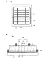
図1(A)に本発明に係る光電変換装置100の上面の模式図を示し、図1(B)に断面の模式図を示す。なお、図1(B)は、図1(A)中のO−P切断線に対応する断面図の一例である。
(Embodiment 1)
FIG. 1A shows a schematic diagram of an upper surface of a
本形態で示す光電変換装置100は、単結晶シリコン層を有するユニットセル116が支持基板102上に設けられている。ユニットセル116の支持基板102側には第1電極106が設けられ、該ユニットセル116の支持基板102側と反対側の表面側には第2電極120が設けられている。ユニットセル116は、第1電極106と第2電極120との間に挟持されている。また、支持基板102とユニットセル116との間には絶縁層104が設けられている。ユニットセル116と絶縁層104との間に第1電極106が設けられ、ユニットセル116の支持基板102側と反対側の表面に第2電極120が設けられている。また、第1電極106と電気的に接続して補助電極118が設けられている。本形態に係る光電変換装置100は、支持基板102上にユニットセル116が固定される構成であり、正極となる電極と、正極に対して負極となる電極は支持基板102の同じ面側に設ける構成が採用される。また、正極となる電極に接続する電極、又は負極となる電極に接続する電極を設ける場合は、正極となる電極および負極となる電極と同様に、支持基板の同じ側の面に設ける構成を採用すればよい。なお、正極となる電極に接続する電極および負極となる電極に接続する電極は必ずしも設ける必要はなく、いずれか一方のみ設ける構成としてもよい。
In the
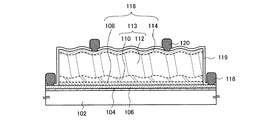
ユニットセル116は、一導電型の第1不純物シリコン層108と、単結晶シリコン層113と、前記一導電型とは逆の導電型の第2不純物シリコン層114が順に積層された構造を有する。なお、第2不純物シリコン層114と第1単結晶シリコン層110の導電型が逆の関係にあれば、第1不純物シリコン層108を設けない構成とすることも可能である。
The
単結晶シリコン層113は、第1単結晶シリコン層110と第2単結晶シリコン層112とからなる。第1単結晶シリコン層110は、単結晶シリコン基板を薄片化した単結晶シリコン層である。第2単結晶シリコン層112は、単結晶シリコン基板を薄片化して得た単結晶シリコン層のエピタキシャル成長層である。
The single
第1単結晶シリコン層110は、単結晶シリコン基板を薄片化して形成する。例えば、単結晶シリコン基板の所定の深さに、水素を含む原料ガスにより生成されるイオン又はクラスターイオンを照射して高濃度の水素を注入し、その後熱処理を行うことにより表層の単結晶シリコン層を分離して形成することができる。また、多孔質シリコン層上に単結晶シリコン層をエピタキシャル成長させた後、多孔質半導体層をウォータージェットで劈開して分離する方法を適用してもよい。第1単結晶シリコン層110は、薄片化する単結晶シリコン基板がp型基板であればp型となり、n型基板であればn型となる。
The first single
第2単結晶シリコン層112は、大気圧プラズマCVD法により、第1単結晶シリコン層110上にシリコン層を成膜すると同時にエピタキシャル成長させることで得ることができる。具体的には、大気圧或いは大気圧近傍の圧力下でプラズマを生成し、原料ガスを活性化させてシリコン層の成膜を行うことにより、単結晶シリコン層を気相エピタキシャル(Vapor Phase Epitaxy)成長させる。
The second single
第2単結晶シリコン層112は、第1単結晶シリコン層110をエピタキシャル成長させており、そのため両者は結晶面、結晶軸(結晶方位)がほぼ揃った結晶となる。また、エピタキシャル成長層である第2単結晶シリコン層112は、真性(i型)となる。
The second single
単結晶シリコン層113は、光電変換を行う領域であり、太陽光を吸収するため、少なくとも厚さ1μm以上とする。例えば、単結晶シリコン層113は、厚さ1μm乃至20μm、好ましくは1μm乃至10μmとする。
The single
一導電型の第1不純物シリコン層108と、第1不純物シリコン層とは逆の導電型の第2不純物シリコン層114は、所定の導電型を付与する不純物元素が添加されたシリコン層である。第1不純物シリコン層108をp型とする場合、第2不純物シリコン層114はn型である。もちろん、第1不純物シリコン層108をn型とし、第2不純物シリコン層114をp型とすることもできる。p型を付与する不純物元素としてはホウ素、アルミニウムなどの元素周期表第13族元素が適用され、n型不純物元素としてはリン、ヒ素などの元素周期表第15族元素が適用される。不純物元素の添加は、イオン注入若しくはイオンドーピングで行うことができる。
The first
本明細書では、「イオン注入」は原料ガスから生成されるイオンを質量分離して対象物に照射する方式を指し、「イオンドーピング」とは原料ガスから生成されるイオンを質量分離せず対象物に照射する方式を指す。 In this specification, “ion implantation” refers to a method in which ions generated from a source gas are mass-separated and irradiated onto an object, and “ion doping” refers to a target without mass-separating ions generated from the source gas. Refers to the method of irradiating an object.
第1電極106と第2電極120は、一方が正極、他方が負極に対応する電極である。第1電極106は、ユニットセル116の第1不純物シリコン層108側に設けられている。また、第2電極120は、ユニットセル116の第2不純物シリコン層114側に設けられている。また、第1電極106と接して補助電極118が形成されている。補助電極118は、第2電極120と同じ面側に設ける構成となる。
One of the
本形態で示す光電変換装置は、第2電極120が形成された側を光入射面とし、第2電極120は、図1(A)に示すように上面から見たときに格子状(或いは櫛状、櫛形、櫛歯状)の電極とする。このような形状とするのは、ユニットセル116に光が入射する有効面積をできるだけ大きくするためである。本形態に係る光電変換装置は、第2電極120側から光を入射するため、ユニットセル116表面を覆う第2電極120の面積をできるだけ小さくし、可能な限りユニットセル116の表面を広く露出させることが好ましい。
In the photoelectric conversion device shown in this embodiment mode, the side on which the
ユニットセル116を固定する支持基板102は、絶縁表面を有する基板若しくは絶縁基板を適用することができる。例えば、アルミノシリケートガラス、アルミノホウケイ酸ガラス、バリウムホウケイ酸ガラスのような電子工業用に使われる各種ガラス基板、石英基板、セラミック基板、又はサファイヤ基板などを適用することができる。好ましくは、大面積化が可能で、安価なガラス基板を適用する。
As the supporting
絶縁層104は、支持基板102とユニットセル116との間に設けられ、両者を固定する役割を果たす。ここでは、絶縁層104と支持基板102とが接合し、ユニットセル116を支持基板102上に固定している。つまり、絶縁層104はユニットセル116と支持基板102とを接合する接合層として機能できる。例えば、絶縁層104は、最表面を形成する層の成膜時の平均面粗さRa値が0.5nm以下、好ましくは0.3nm以下とする。なお、本明細書における平均面粗さ(Ra値)とは、JIS B0601で定義されている中心線平均粗さを面に対して適用できるよう3次元に拡張したものである。
The insulating
次に、本形態に係る光電変換装置100の製造方法の一例について、図2〜図4を参照して説明する。
Next, an example of a method for manufacturing the
単結晶シリコン基板101の一表面側から所定の深さの領域に脆化層103を形成する。また、単結晶シリコン基板101の一表面側に第1不純物シリコン層108、第1電極106及び絶縁層104を形成する。
An
脆化層103、第1不純物シリコン層108、第1電極106および絶縁層104の形成順序や形成方法は一通りでなく、少なくとも以下に示す(1)〜(4)が挙げられる。(1)単結晶シリコン基板の一表面上に保護層を形成し、該保護層が形成された面側からイオン又はクラスターイオンを照射して単結晶シリコン基板の所定の深さの領域に脆化層を形成した後、続けて保護層が形成された面側から一導電型を付与する不純物元素を添加して単結晶シリコン基板の一表面側に第1不純物シリコン層を形成する。保護層を除去した後、該保護層が形成されていた表面側である第1不純物シリコン層上に第1電極を形成し、該第1電極上に絶縁層を形成する。(2)単結晶シリコン基板の一表面上に保護層を形成し、該保護層が形成された面側から一導電型を付与する不純物元素を添加して単結晶シリコン基板の一表面側に第1不純物シリコン層を形成した後、続けて保護層が形成された面側からイオン又はクラスターイオンを照射して単結晶シリコン基板の所定の深さの領域に脆化層を形成する。保護層を除去した後、該保護層が形成されていた表面側である第1不純物シリコン層上に第1電極を形成し、該第1電極上に絶縁層を形成する。(3)単結晶シリコン基板の一表面上に第1電極を形成した後、該第1電極が形成された面側からイオン又はクラスターイオンを照射して単結晶シリコン基板の所定の深さの領域に脆化層を形成する。さらに、第1電極が形成された面側から一導電型を付与する不純物元素を添加して単結晶シリコン基板の一表面側に第1不純物シリコン層を形成する。第1電極上に絶縁層を形成する。(4)単結晶シリコン基板の一表面上に第1電極を形成した後、該第1電極が形成された面側から一導電型を付与する不純物元素を添加して単結晶シリコン基板の一表面側に第1不純物シリコン層を形成する。さらに、第1電極が形成された面側からイオン又はクラスターイオンを照射して単結晶シリコン基板の所定の深さの領域に脆化層を形成する。第1電極上に絶縁層を形成する。本形態では、(1)の形成順序を適用して説明する。
The formation order and formation method of the
単結晶シリコン基板101の一表面上に保護層105を形成した後、保護層105が形成された面側からイオン又はクラスターイオンを照射して、単結晶シリコン基板101の一表面側から所定の深さの領域に脆化層103を形成する(図2(A)参照)。
After forming the
単結晶シリコン基板101は、平面形状は特に限定されないが、後に固定する支持基板が矩形の場合はほぼ四辺形とすることが好ましい。例えば、単結晶シリコン基板101として、p型で抵抗率1Ωcm乃至40Ωcm程度の単結晶シリコン基板を用いることができる。また、単結晶シリコン基板に代えて多結晶シリコン基板を適用してもよい。
The single
一般に流通している単結晶シリコン基板は円形状のものが多いが、そのまま用いてもよいし、円形状から所望の形状に切り出すこともできる。例えば、図5(A)に示すように円形の単結晶シリコン基板101aを適用してもよいし、図5(B)、(C)に示すようにほぼ四辺形の単結晶シリコン基板101b、単結晶シリコン基板101cを切り出してもよい。図5(B)に示す場合は、円形の単結晶シリコン基板101aに内接する大きさで最大となるように矩形の単結晶シリコン基板101bを切り出す例である。単結晶シリコン基板101bの角部の頂点の角度はほぼ90°である。図5(C)に示す場合は、円形の単結晶シリコン基板101aに内接する最大の矩形領域よりも対辺の間隔が長くなるように単結晶シリコン基板101cを切り出す例である。単結晶シリコン基板101cの角部の頂点の角度は90°とはならず、単結晶シリコン基板101cは矩形ではなく多角形状となる。また、図5(D)に示すように、六角形の単結晶シリコン基板101dを切り出してもよい。図5(D)に示す場合は、円形の単結晶シリコン基板101aに内接する大きさで最大となるように六角形の単結晶シリコン基板101dを切り出す例である。六角形に切り出すことで、矩形とするよりも、切り代となり無駄になる原料を減らすことができる。また、1枚の支持基板に複数の光電変換層を形成し、太陽電池モジュールを形成する場合、光電変換層を形成する単結晶シリコン層を六角形とすることで、他の多角形よりも敷き詰めることが容易であり、隙間なく貼り合わせることができる。
In general, single crystal silicon substrates in circulation are mostly circular, but they may be used as they are or cut out from a circular shape into a desired shape. For example, a circular single
保護層105は、脆化層103や第1不純物シリコン層108を形成する際に単結晶シリコン基板101表面がエッチングされる、或いは損傷するのを防ぐための層であり、酸化シリコン層、窒化シリコン層、酸化窒化シリコン層又は窒化酸化シリコン層などで形成する。例えば、オゾン水、過酸化水素水又はオゾン雰囲気により、単結晶シリコン基板101表面に厚さ2nm乃至5nmのケミカルオキサイドを保護層105として形成する。熱酸化法や酸素ラジカル処理により、単結晶シリコン基板101表面に厚さ2nm乃至10nmの酸化層を保護層105として形成してもよい。また、プラズマCVD法により、厚さ2nm乃至10nmの保護層105を形成してもよい。
The
なお、本明細書における酸化窒化シリコン層とは、組成として窒素よりも酸素の含有量が多く、ラザフォード後方散乱法(RBS:Rutherford Backscattering Spectrometry)及び水素前方散乱法(HFS:Hydrogen Forward Scattering)を用いて測定した場合に、組成範囲として酸素が50atoms%乃至70atoms%、窒素が0.5atoms%乃至15atoms%、Siが25atoms%乃至35atoms%、水素が0.1atoms%乃至10atoms%の範囲で含まれるものをいう。また、窒化酸化シリコン層とは、組成として酸素よりも窒素の含有量が多く、RBS及びHFSを用いて測定した場合に、酸素が5atoms%乃至30atoms%、窒素が20atoms%乃至55atoms%、Siが25atoms%乃至35atoms%、水素が10atoms%乃至30atoms%の範囲で含まれるものをいう。 Note that the silicon oxynitride layer in this specification has a higher oxygen content than nitrogen as a composition, and uses Rutherford Backscattering Spectroscopy (RBS) and Hydrogen Forward Scattering (HFS). As a composition range, oxygen is included in the range of 50 to 70 atoms%, nitrogen is in the range of 0.5 to 15 atoms%, Si is in the range of 25 to 35 atoms%, and hydrogen is in the range of 0.1 to 10 atoms%. Say. The silicon nitride oxide layer has a nitrogen content higher than that of oxygen as a composition. When measured using RBS and HFS, oxygen is 5 atoms% to 30 atoms%, nitrogen is 20 atoms% to 55 atoms%, and Si is This means that 25 to 35 atoms% and hydrogen is contained in the range of 10 to 30 atoms%.
脆化層103は、イオン又はクラスターイオンを照射して、単結晶シリコン基板101の所定の深さの領域に形成する。イオン又はクラスターイオンは、水素を含む原料ガスにより生成する。水素を含む原料ガスにより生成されるイオン又はクラスターイオンとしては、H+イオン、H2 +イオン、H3 +イオンが挙げられる。好ましくは、H3 +イオンの割合を高めて用いることが好ましい。H3 +イオンを用いることで水素の注入効率を向上することができる。イオン又はクラスターイオンの加速電圧及びドーズ量を制御し照射することで、単結晶シリコン基板101の所定の深さの領域に局所的に高濃度の水素を注入して脆化層103を形成することができる。脆化層103には、水素原子換算で5×10²⁰atoms/cm3以上の水素を含ませることが好ましい。
The
単結晶シリコン基板101から分離される単結晶シリコン層の厚さ、つまり後に支持基板に固定される第1単結晶シリコン層110の厚さは、脆化層103を形成する深さにより決定される。脆化層103の深さは、イオン又はクラスターイオンを照射する際の加速電圧によって制御できる。単結晶シリコン基板101から分離される単結晶シリコン層が薄いほど、残る単結晶シリコン基板は厚くなり、その結果繰り返し利用できる回数を増やすことができる。しかし、分離する単結晶シリコン層を薄くするためには脆化層103を浅い領域に形成しなければならず、加速電圧を低くしなければならない。加速電圧を低くするとイオンの照射時間が長くなり、タクトタイムが悪化するため、生産性などを考慮した深さに脆化層103を形成する必要がある。
The thickness of the single crystal silicon layer separated from the single
H3 +イオンを利用することで、H+イオンと比較して、脆化層103を単結晶シリコン基板101の浅い領域に容易に形成することができる。例えば、単結晶シリコン基板101の一表面側から深さAの領域に脆化層103を形成する。H+イオンの加速電圧をBとすると、H3 +イオンの加速電圧は約3Bとすることができる。これは、H3 +イオンが単結晶シリコン基板に照射された際に、単結晶シリコン基板或いはその上層を構成する原子と衝突してH原子やH+イオンなどに分離されるためと考えられる。よって、H3 +イオンを利用することで分離する単結晶シリコン層を薄くすることが容易になり、生産性を低下させることなく繰り返し利用の回数を増やすことができる。
By using H 3 + ions, the
H3 +イオンに代表されるクラスターイオンのドーピングは、水素を含む原料ガスにより水素プラズマを生成し、該水素プラズマ中に生成されるクラスターイオンを質量分離せずに電圧によって加速することにより照射するイオンドーピング装置を用いて行うことができる。イオンドーピング装置を用いることにより、大面積な単結晶シリコン基板101に対しても均一なドーピングを行うことができる。
In the doping of cluster ions typified by H 3 + ions, irradiation is performed by generating hydrogen plasma with a source gas containing hydrogen, and accelerating the cluster ions generated in the hydrogen plasma by voltage without mass separation. An ion doping apparatus can be used. By using an ion doping apparatus, uniform doping can be performed even on the single
例えば、H3 +イオンを主に用いて、ドーズ量1×10¹⁶ions/cm2乃至5×1016ions/cm2でイオンドーピング法によりイオン又はクラスターイオンを照射し、脆化層103を形成することができる。水素原子換算では、3×1016atoms/cm2乃至1.5×1017atoms/cm2の範囲で添加して、脆化層103を形成することができる。
For example, the
なお、図2(A)に示すように、イオン又はクラスターイオンを保護層105に照射し、保護層105を通過させて水素を注入させることで、単結晶シリコン基板101表面がエッチングされるなど損傷を受けるのを防ぐことができる。
Note that as shown in FIG. 2A, the surface of the single
ここで、図6に、イオン源2000において生成された複数の種類のイオンを、質量分離せずに単結晶シリコン基板101に照射するイオンドーピング装置の構成を説明する概略図の一例を示す。イオン源2000にはガス供給部2004から水素等の所定の原料ガスが供給される。イオン源2000にはフィラメント2001が備えられている。フィラメント電源2002はフィラメント2001へアーク放電電圧を印加し、フィラメント2001に流れる電流を調節する。ガス供給部2004から供給された原料ガスは、排気系により排気される。
Here, FIG. 6 shows an example of a schematic diagram illustrating a configuration of an ion doping apparatus that irradiates the single
イオン源2000で生成されたイオンは、引出し電極系2005によって引き出され、イオンビーム2017を形成する。イオンビーム2017は、載置台2006に置かれた単結晶シリコン基板101に照射される。イオンビーム2017に含まれるイオン種の割合は載置台2006の近傍に設けられた質量分析管2007によって計量される。質量分析管2007によって計量されたイオン密度は、質量分析計2008で信号変換され、その結果を電源制御部2003にフィードバックさせるようにしても良い。電源制御部2003はイオン密度の計量結果に従って、フィラメント電源2002を制御することができる。
Ions generated by the
図6で示すように、ガス供給部2004から供給された水素等の原料ガスは、イオンドーピング装置のチャンバー内を流れ、排気系によって排出される構成となっている。
As shown in FIG. 6, the source gas such as hydrogen supplied from the
クラスターイオンであるH3 +イオンを多量に発生させたイオンビームを基板に照射することで、H+イオン、H2 +イオンを照射するよりも水素の注入効率が向上し、ドーズ量が少なくても水素を単結晶シリコン基板101に高濃度に注入することができるという効果を奏する。
By irradiating the substrate with an ion beam in which a large amount of H 3 + ions, which are cluster ions, is generated, the hydrogen implantation efficiency is improved and the dose amount is smaller than when irradiating H + ions and H 2 + ions. Also, there is an effect that hydrogen can be injected into the single
このようにH3 +イオンの割合を高めておくことで、脆化層103には1×10²⁰atoms/cm3以上、好ましくは5×1020atoms/cm3の水素を含ませることが可能である。単結晶シリコン基板101に局所的に高濃度の水素注入領域を形成すると、結晶構造が失われ微小な空洞が形成されるため、単結晶シリコン基板101に形成される脆化層103は多孔質構造となっている。そのため、比較的低温(600℃以下)の熱処理によって脆化層103に形成された微小な空洞の体積変化が起こり、脆化層103に沿って単結晶シリコン基板101を分離することができる。脆化層103に含まれる水素濃度は、イオン又はクラスターイオンのドーズ量や加速電圧などによって制御される。
By increasing the ratio of H 3 + ions in this way, the
なお、略四辺形で形成される単結晶シリコン基板101の一辺の長さよりも長い線状イオンビームにより、単結晶シリコン基板101の表面を走査してイオン又はクラスターイオンを打ち込めば、脆化層103が形成される深さを均一なものとすることができる。
Note that if the surface of the single
次に、保護層105が形成された面側から一導電型を付与する不純物元素を添加し、単結晶シリコン基板101の一表面側に第1不純物シリコン層108を形成する(図2(B)参照)。不純物元素は保護層105を通過して単結晶シリコン基板101に添加し、単結晶シリコン基板101と保護層105との間に第1不純物シリコン層108を形成する。
Next, an impurity element imparting one conductivity type is added from the surface side where the
第1不純物シリコン層108は、一導電型を付与する不純物元素をイオンドーピング法又はイオン注入法により添加して形成する。例えば、一導電型を付与する不純物元素としてホウ素を添加し、p型の第1不純物シリコン層108を形成する。ホウ素の添加は、B2H6、BF3を原料ガスとして、生成されたイオンを質量分離しないで電圧で加速して、生成されるイオン流を基板に照射するイオンドーピング装置を用いて行うことが好ましい。なお、一導電型を付与する不純物元素を添加する原料ガスには、水素や、希ガスを添加してもよく、例えばこの場合、B2H6又はBF3に水素やヘリウムを添加したものを原料ガスとしてもよい。単結晶シリコン基板101の面積が、対角300mmを超えるような大きさであってもイオンビームの照射面積を大きくすることができ、効率良く処理できるからである。例えば、長辺の長さが300mmを超える線状イオンビームを形成し、該線状イオンビームが、単結晶シリコン基板101の一端から他端まで照射されるように処理すれば、単結晶シリコン基板101の全面に第1不純物シリコン層108を均一に形成することができる。第1不純物シリコン層108は、厚さ30nm乃至150nm、好ましくは50nm乃至100nmで形成する。
The first
また、第1不純物シリコン層108は、単結晶シリコン又は多結晶シリコンに限定されず、微結晶シリコン又は非晶質シリコンで形成してもよい。例えば、第1不純物シリコン層108は、プラズマCVD法によりシラン系ガスにジボランなどホウ素を含むドーピングガスを添加した原料ガスを用いて形成することができる。第1不純物シリコン層108をプラズマCVD法により形成する場合は、保護層105を形成する前で、単結晶シリコン基板101表面上に形成された自然酸化層などは除去してから形成する。なお、第1不純物シリコン層108を微結晶シリコン又は非晶質シリコンで形成する場合は、キャリアの再結合を防ぐため薄く形成することが好ましい。
The first
第1不純物シリコン層108は、本形態で示す光電変換装置において、光入射側と反対側に配置され、裏面電界(BSF;Back Surface Field)を形成することができる。単結晶シリコン基板101としてp型基板を適用すれば、別途p型を付与する不純物元素を添加した不純物シリコン層(本形態では第1不純物シリコン層108)を設けなくともよい。しかし、高濃度p型領域(p+型と表記する)とそれよりも低濃度のp型領域の配置とすることで、BSFを形成できる。ここでは、p+型となる第1不純物シリコン層108とp型の第1単結晶シリコン層110の配置となり、光閉じこめ効果により、光励起により生成されたキャリア(電子と正孔)の再結合を防ぎキャリア収集効率を高めることができる。よって、光電変換装置の光電変換効率を向上させることができる。
In the photoelectric conversion device described in this embodiment mode, the first
次に、保護層105を除去した後、第1不純物シリコン層108上に第1電極106を形成する(図2(C)参照)。
Next, after the
第1電極106は、後に単結晶シリコン基板101を分離するための熱処理温度に耐えうる材料を用いる必要があり、高融点金属であることが好ましい。具体的には、支持基板102の歪み点温度程度の耐熱性が必要である。例えば、チタン、モリブデン、タングステン、タンタル、クロム又はニッケルなどの金属材料を適用する。また、前述の金属材料と、金属材料の窒化物との積層構造とすることもできる。例えば、窒化チタン層とチタン層、窒化タンタル層とタンタル層、窒化タングステン層とタングステン層などの積層構造が挙げられる。窒化物との積層構造とする場合は、第1不純物シリコン層108と接して窒化物を形成する。窒化物を形成することで、第1電極106と第1不純物シリコン層108との密着性を向上させることができる。また、第1電極106表面は、平均面粗さRa値が0.5nm以下、好ましくは0.3nm以下であるとよい。もちろん、平均面粗さRa値が小さくなるほど好ましいのはいうまでもない。第1電極106表面が平滑性に優れることで、支持基板102との貼り合わせを良好に行うことができる。もちろん、上層に接合層として機能する絶縁層104を形成することで平滑性に優れた接合面とすることができるが、下層の第1電極106の平滑性が良好であれば、上層の絶縁層104の平滑性も良好としやすい。また、場合によっては、接合層として機能する絶縁層を設けなくとも、第1電極106と支持基板との間で直接接合を形成することも可能となる。具体的には、チタンを用いて第1電極106を形成すると表面の平滑性に優れるため好ましい。第1電極106は、蒸着法やスパッタリング法により、膜厚100nm以上で形成することができる。なお、第1不純物シリコン層108上に自然酸化層などが形成されている場合は、除去してから第1電極106を形成する。
The
第1電極106上に絶縁層104を形成する(図2(D)参照)。絶縁層104は単層構造としても2層以上の積層構造としてもよいが、最表面(接合面)は平滑性を有することが好ましく、平滑性且つ親水性表面を有するとより好ましい。絶縁層104の最表面(接合層)の平滑性は、具体的には平均面粗さRa値が0.5nm以下、好ましくは0.3nm以下となるように形成すると支持基板との貼り合わせが良好に行うことができる。もちろん、平均面粗さRa値は小さくなるほど好ましいのはいうまでもない。例えば、絶縁層104として、酸化シリコン層、窒化シリコン層、酸化窒化シリコン層又は窒化酸化シリコン層を形成する。絶縁層104の形成方法は、プラズマCVD法、光CVD法、又は熱CVD法(減圧CVD法又は常圧CVD法も含む)などのCVD法を適用すればよく、好ましくはプラズマCVD法を適用することで好適な平滑性を有する層を形成できる。
The insulating
平滑性を有し親水性表面を形成できる層としては、例えば有機シラン系ガスを成膜用の原料ガスに用いてプラズマCVD法により形成される酸化シリコン層が好ましい。このような酸化シリコン層を用いることによって、支持基板と後に形成されるユニットセルとの接合を強固にすることができる。有機シラン系ガスとしては、テトラエトキシシラン(TEOS:化学式Si(OC2H5)4)、テトラメチルシラン(TMS:化学式Si(CH3)4)、テトラメチルシクロテトラシロキサン(TMCTS)、オクタメチルシクロテトラシロキサン(OMCTS)、ヘキサメチルジシラザン(HMDS)、トリエトキシシラン(SiH(OC2H5)3)、トリスジメチルアミノシラン(SiH(N(CH3)2)3)等のシリコン含有化合物を用いることができる。 As a layer having smoothness and capable of forming a hydrophilic surface, for example, a silicon oxide layer formed by a plasma CVD method using an organic silane-based gas as a film forming raw material gas is preferable. By using such a silicon oxide layer, the bonding between the support substrate and a unit cell to be formed later can be strengthened. Examples of the organic silane gas include tetraethoxysilane (TEOS: chemical formula Si (OC 2 H 5 ) 4 ), tetramethylsilane (TMS: chemical formula Si (CH 3 ) 4 ), tetramethylcyclotetrasiloxane (TMCTS), and octamethyl. Silicon-containing compounds such as cyclotetrasiloxane (OMCTS), hexamethyldisilazane (HMDS), triethoxysilane (SiH (OC 2 H 5 ) 3 ), trisdimethylaminosilane (SiH (N (CH 3 ) 2 ) 3 ) Can be used.
また、平滑性を有し親水表面を形成できる層として、シラン、ジシラン、又はトリシラン等のシラン系ガスを成膜用の原料ガスに用いてプラズマCVD法により形成される酸化シリコン、酸化窒化シリコン、窒化シリコン、窒化酸化シリコンを用いることもできる。例えば、成膜用の原料ガスにシランとアンモニアを用いてプラズマCVD法により形成する窒化シリコン層を適用することができる。前記原料ガスに水素を加えてもよい。また、シランとアンモニアに加え、亜酸化窒素を原料ガスに添加して、プラズマCVD法により窒化酸化シリコン層を形成することができる。 Further, as a layer having smoothness and capable of forming a hydrophilic surface, silicon oxide, silicon oxynitride formed by a plasma CVD method using a silane-based gas such as silane, disilane, or trisilane as a raw material gas for film formation, Silicon nitride or silicon nitride oxide can also be used. For example, a silicon nitride layer formed by a plasma CVD method using silane and ammonia as a film forming source gas can be used. Hydrogen may be added to the source gas. In addition to silane and ammonia, nitrous oxide can be added to a source gas, and a silicon nitride oxide layer can be formed by a plasma CVD method.
例えば、絶縁層104として、膜厚50nmの酸化窒化シリコン層、膜厚50nmの窒化酸化シリコン層、及び膜厚50nmの酸化シリコン層の積層膜を形成する。これら絶縁層はプラズマCVD法により形成することができる。最表面を形成する層であり、接合面となる酸化シリコン層は、成膜後の表面のRa値0.4nm以下、好ましくは0.3nm以下となるようにすることが好ましく、例えば原料ガスにTEOSを用いてプラズマCVD法により形成する。また、絶縁層104に窒素を含むシリコン絶縁層、具体的には窒化シリコン層や窒化酸化シリコン層を含むことで、後に貼り合わせる支持基板102からの不純物拡散を防ぐこともできる。
For example, a stacked film of a silicon oxynitride layer with a thickness of 50 nm, a silicon nitride oxide layer with a thickness of 50 nm, and a silicon oxide layer with a thickness of 50 nm is formed as the insulating
いずれにしても、最表面が平滑性を有し、具体的には平均面粗さRa値0.5nm以下、好ましくは0.3nm以下の平滑性を有する絶縁層であれば、シリコンを含む絶縁層に限らず適用することができる。なお、絶縁層104を積層構造とする場合は、最表面を形成する層以外はこの限りではない。また、絶縁層104の成膜温度は単結晶シリコン基板101に形成した脆化層103から水素が脱離しない温度とする必要があり、好ましくは350℃以下の成膜温度とする。
In any case, if the outermost surface has smoothness, specifically, an insulating layer having smoothness with an average surface roughness Ra value of 0.5 nm or less, preferably 0.3 nm or less, an insulating layer containing silicon is used. It can be applied not only to layers. Note that in the case where the insulating
単結晶シリコン基板101の一表面側と、支持基板102の一表面側と、を対向させ、接合面となる面を重ね合わせて貼り合わせる(図2(E)参照)。本形態では、単結晶シリコン基板101に形成された絶縁層104と、支持基板102の一表面側と、を接触させて接合する。接合面は、絶縁層104の一表面(第1電極106と接していない面側)と、支持基板102の一表面となる。
One surface side of the single
接合面(本形態では絶縁層104の一表面および支持基板102の一表面)は十分に清浄化しておく。これは、接合面に微小なゴミなどのパーティクルが存在すると貼り合わせ不良の要因となるからである。具体的には、接合面をそれぞれ洗浄して清浄化することが好ましい。例えば、周波数100kHz乃至2MHzの超音波と純水を用いた超音波洗浄、メガソニック洗浄、又は窒素と乾燥空気と純水を用いた2流体洗浄を行って、接合面を清浄化する。また、洗浄に用いる純水に二酸化炭素などを添加して、抵抗率を5MΩcm以下に下げ静電気の発生を防ぐようにしてもよい。
The bonding surfaces (one surface of the insulating
単結晶シリコン基板101側の接合面と、支持基板102側の接合面を接触させて接合する。本形態では、絶縁層104の一表面側と、支持基板102の一表面側と、を接触させて接合する。接合は、ファン・デル・ワールス力や水素結合が作用して形成される。例えば、重ね合わせた単結晶シリコン基板101と支持基板102の一箇所を押圧することで、接合面全域にファン・デル・ワールス力や水素結合を広げることができる。接合面の一方又は双方が親水表面を有する場合は、水酸基や水分子が接着剤として働き、後の熱処理で水分子が拡散し、残留成分がシラノール基(Si−OH)を形成して水素結合により接合を形成する。さらにこの接合部は、水素が抜けることでシロキサン結合(O−Si−O)を形成して共有結合となり、より強固な接合となる。接合面は、両基板(単結晶シリコン基板101と支持基板102)側のそれぞれの接合面(絶縁層104の一表面と支持基板102の一表面)の平均面粗さRa値が0.5nm以下、好ましくは0.3nm以下であるとよい。また、両基板の接合面の平均面粗さRa値の合計が0.7nm以下、好ましくは0.6nm以下、より好ましくは0.4nm以下であるとよい。さらに、両基板のそれぞれの接合面の純水に対する接触角が20°以下、好ましくは10°以下、より好ましくは5°以下であり、両基板の接合面の純水に対する接触角の合計が30°以下、好ましくは20°以下、より好ましくは10°以下であるとよい。接合面がこれらの条件を満たすと、貼り合わせを良好に行うことができ、より強固な接合を形成できる。
The bonding surface on the single
また、支持基板102と単結晶シリコン基板101の貼り合わせを良好に行うために、接合面を活性化しておいてもよい。例えば、接合面の一方又は双方に原子ビーム若しくはイオンビームを照射する。原子ビーム若しくはイオンビームを利用する場合には、アルゴン等の不活性ガス中性原子ビーム若しくは不活性ガスイオンビームを用いることができる。その他に、プラズマ処理若しくはラジカル処理を行うことで接合面を活性化することもできる。このような表面処理により、400℃以下の温度であっても異種材料間の接合を形成することが容易となる。また、接合面をオゾン添加水、酸素添加水、水素添加水、又は純水等で洗浄処理してもよい。このような洗浄処理をすることで接合面を親水性にすることができ、接合面の水酸基を増大させ、接合をより強固にすることが可能である。
Further, the bonding surface may be activated in order to favorably bond the supporting
また、単結晶シリコン基板101と支持基板102とを貼り合わせた後は、熱処理又は加圧処理を行うことが好ましい。熱処理又は加圧処理を行うことで接合強度を高めることができる。熱処理を行う際は、その温度範囲は支持基板102の歪み点温度以下で、且つ単結晶シリコン基板101に形成した脆化層103で体積変化が起きない温度とし、好ましくは200℃以上410℃未満とする。なお、この熱処理は、後の脆化層103を境として単結晶シリコン基板101の一部を分離するための熱処理と連続して行ってもよい。また、貼り合わせを行った装置或いは場所で、そのまま連続して200℃以上の熱処理を行い、接合を強固にすることが好ましい。また、加圧処理する場合は、接合面に垂直な方向に圧力が加わるように行い、支持基板102及び単結晶シリコン基板101の耐圧性を考慮して行う。
In addition, after the single
なお、支持基板102側にも絶縁層を形成しておき、支持基板102上に形成した絶縁層を接合面としてもよい。また、支持基板102側に窒化シリコン層や窒化酸化シリコン層などの窒素を含有するシリコン絶縁層を形成しておいてもよい。窒素を含有するシリコン絶縁層は、支持基板102からの不純物汚染を防止するブロッキング層として機能できる。
Note that an insulating layer may be formed on the supporting
熱処理を行い、脆化層103又は当該脆化層103近傍を境として、支持基板102から単結晶シリコン基板101の一部を分離する。支持基板102上には単結晶シリコン基板101から分離した第1単結晶シリコン層110が残存し、所謂SOI構造が得られる。第1単結晶シリコン層110は、単結晶シリコン基板101とほぼ同じ結晶性を有する。また、第1単結晶シリコン層110が分離された剥離基板130が得られる(図3(A)参照)。
Heat treatment is performed to separate part of the single
脆化層103を境として、単結晶シリコン基板101から第1単結晶シリコン層110を分離する熱処理は、410℃以上支持基板102の歪み点温度未満で行うことが好ましい。また、絶縁層104の成膜温度以上で行うことが好ましい。熱処理温度を600℃以上、好ましくは630℃以上支持基板102の歪み点温度未満とすれば、支持基板102を歪ませることなく、第1不純物シリコン層108に含まれる不純物元素を活性化することができる。例えば、450℃以上700℃未満の温度範囲で熱処理を行うことにより、脆化層103に形成された微小な空洞の体積変化が起こり、脆化層103に沿って分離する。絶縁層104は支持基板102と接合しているので、支持基板102上に第1単結晶シリコン層110が形成される。第1単結晶シリコン層110の厚さは脆化層103の形成深さにほぼ対応する。また、支持基板102と第1単結晶シリコン層110の間には、絶縁層104、第1電極106、第1不純物シリコン層108が形成されている。
The heat treatment for separating the first single
なお、第1単結晶シリコン層110の分離面となった表面は、平均面粗さRa値が7nm乃至10nm、最大高低差(P−V)が300nm乃至400nmの凹凸が形成される場合がある。ここでいう最大高低差とは、山頂と谷底の高さの差を示す。また、ここでいう山頂と谷底とはJIS B0601で定義されている「山頂」「谷底」を三次元に拡張したものであり、山頂とは指定面の山において最も標高の高いところ、谷底とは指定面の谷において最も標高の低いところと表現される。第1単結晶シリコン層110表面の凹凸は、その上層に形成されていく層にも反映することができ、完成する光電変換装置の光入射面となる最上層(本形態では第2不純物シリコン層)に凹凸を形成することができる。半導体表面における反射率は、波長依存性はあるものの、通常30%〜50%といわれる。光入射面での反射は入射する光の損失となり、光電変換効率が低下する要因となる。よって、光入射面に凹凸が形成されれば、表面テクスチャにより反射率を低減し、光閉じ込め効果により光電変換効率を向上することができる。
Note that the surface which is the separation surface of the first single
第1単結晶シリコン層110が分離された単結晶シリコン基板である剥離基板130は、再生処理を行った後、繰り返し利用することができる。剥離基板130は、光電変換装置を製造する単結晶シリコン基板として利用しても良いし、その他の用途に流用してもよい。単結晶シリコン層を分離するための単結晶シリコン基板として繰り返し利用すれば、1枚の原料基板から複数個の光電変換装置を製造できる。また、分離する第1単結晶シリコン層110の厚さを薄くするほど、剥離基板130を厚くすることができ、繰り返し利用する回数を増やせ、資源を有効活用できる。
The
単結晶シリコン基板101から薄片化された第1単結晶シリコン層110は、脆化層形成工程や分離工程などのダメージにより結晶欠陥が生成されてしまう。光電変換を行う領域に存在する欠陥はキャリアをトラップする或いは再結合中心となるなど、光電変換効率を低下させる要因となる。また、第1単結晶シリコン層110はエピタキシャル成長を行う際のシード層となるため、結晶欠陥が存在するとうまくエピタキシャル成長が進行しない。よって、単結晶シリコン基板を薄片化して得た単結晶シリコン層に結晶欠陥修復処理又は結晶欠陥除去処理を行う。
In the first single
結晶欠陥修復処理又は結晶欠陥除去処理としては、レーザ処理、RTA(Rapid Thermal Anneal)処理、フラッシュランプ処理、炉での熱処理、エッチング処理、又はCMP処理を適用する。本形態では、レーザ処理により結晶欠陥の低減を図る例を示す(図3(B)参照)。 As the crystal defect repair processing or crystal defect removal processing, laser processing, RTA (Rapid Thermal Anneal) processing, flash lamp processing, furnace heat treatment, etching processing, or CMP processing is applied. In this embodiment mode, an example in which crystal defects are reduced by laser treatment is shown (see FIG. 3B).
第1単結晶シリコン層110にレーザビームを照射して、一部又は全部を溶融し、再結晶化させることで、第1単結晶シリコン層110の結晶欠陥を修復することができる。好ましくは、レーザビームの照射による単結晶シリコン層の溶融は、部分溶融とする。単結晶シリコン層を完全溶融させた場合は、液相となった後の単結晶シリコンが無秩序な核発生により微結晶化し、結晶性が低下するおそれがあるからである。これに対し、単結晶シリコン層を部分溶融させた場合は、溶融されていない固相部分から結晶成長が進行するため、結晶性を低下させることなく、結晶欠陥を修復することができる。なお、本明細書において、完全溶融とは、単結晶シリコン層が下部界面付近まで溶融されて、液相状態になることをいう。部分溶融とは、単結晶シリコン層の一部(例えば上層部)は溶融されて液相となるが、その他(例えば下層部)は溶融せずに固相のままであることをいう。
By irradiating the first single
例えば、図3(B)に示すように、第1単結晶シリコン層110の上面からレーザビーム180を照射することで、第1単結晶シリコン層110の少なくとも表面側は溶融し、固相状態の下層部をシード層として、その後の冷却過程で再結晶化する。その過程で、第1単結晶シリコン層110の結晶欠陥を修復することができる。レーザビーム180としては、例えば、XeClエキシマレーザやYAGレーザの第2高調波を適用することが好ましい。
For example, as shown in FIG. 3B, by irradiating a
ここで、波長が紫外領域であるレーザビーム等の光を照射して結晶欠陥の修復を図る場合は、第1単結晶シリコン層110の膜厚が200nm以下、好ましくは100nm以下と薄い方が好ましい。これは、結晶欠陥の修復を図る単結晶シリコン層の厚さを薄くした方が、結晶欠陥の修復に必要なエネルギーを小さくすることができるからである。
Here, when crystal defects are repaired by irradiating light such as a laser beam having a wavelength in the ultraviolet region, the thickness of the first single
第1単結晶シリコン層110の結晶欠陥を低減する方法としてレーザ処理を適用すると、支持基板102が直接加熱されず、該支持基板102の温度上昇を抑えることができるため好ましい。特に、支持基板102として耐熱性の低いガラス基板を適用する場合には、レーザ処理による結晶欠陥修復が好適である。また、第1単結晶シリコン層110を薄く形成しておくことで、レーザ処理による結晶欠陥の修復を十分に行うことができる。これは、第1単結晶シリコン層110が厚すぎると膜厚方向に深い領域まで十分に溶融させることができずシード層となる領域に結晶欠陥が多く残ってしまう恐れがあるからである。
Applying laser treatment as a method for reducing crystal defects in the first single
また、上記レーザ処理のとき、少なくともレーザビームの照射領域は250℃乃至600℃の温度に加熱されていることが好ましい。照射領域を加熱しておくことで、レーザビームの照射による溶融時間を長くすることができ、欠陥の修復を効果的に行うことができる。レーザビーム180は第1単結晶シリコン層110の表面側を溶融させるものの、支持基板102は殆ど加熱されないので、ガラス基板のような耐熱性の低い支持基板を用いることが可能になる。また、第1電極106を高融点金属で形成することで、上記温度で加熱されても第1単結晶シリコン層110に悪影響を及ぼすことがない。第1電極106を形成する金属と第1不純物シリコン層108の界面ではシリサイドが形成され、より電流が流れ易くなる。また、上記レーザ処理は第1不純物シリコン層108の活性化を兼ねることもできる。
In the laser treatment, it is preferable that at least a laser beam irradiation region is heated to a temperature of 250 ° C. to 600 ° C. By heating the irradiation region, the melting time by the laser beam irradiation can be lengthened, and the defect can be repaired effectively. Although the
また、酸素を含む雰囲気中で、第1単結晶シリコン層110上面にレーザビームを照射することにより、第1単結晶シリコン層110表面に凹凸を形成する、或いは分離面となった表面に既に形成されていた凹凸より最大高低差を大きくすることもできる。
Further, by irradiating the upper surface of the first single
結晶欠陥の低減を図るレーザ処理を行うことのできるレーザ処理装置の一例を、図7を参照して説明する。レーザ処理装置は、レーザ発振器510、レーザビームを細い線状ビームに集光伸張させる光学系511、レーザビーム照射領域の雰囲気を制御するガス噴射筒512、該ガス噴射筒512に雰囲気制御ガスを供給するガス供給部513、流量制御部514、ガス加熱部515、被照射体530(具体的には第1単結晶シリコン層110が固定された支持基板102)を浮遊させ搬送する基板ステージ522、基板の両端を支持して搬送するガイドレール523、基板ステージ522に浮遊用にガスを供給するガス供給部516を備えている。
An example of a laser processing apparatus capable of performing laser processing for reducing crystal defects will be described with reference to FIG. The laser processing apparatus includes a
レーザ発振器510は、その発振波長が、紫外光域乃至可視光域にあるものが選択される。レーザ発振器510は、パルス発振型のArF、KrF又はXeClエキシマレーザ、或いはNd−YAGレーザ、YLFレーザなどの固体レーザで、繰り返し周波数1MHz以下、パルス幅10n秒以上500n秒以下のレーザビームを射出するものが好ましい。例えば、繰り返し周波数10Hz〜300Hz、パルス幅25n秒、波長308nmのレーザビームを射出できるXeClエキシマレーザを用いる。
As the
光学系511はレーザビームを集光及び伸張して、被照射面に断面形状が線状となるレーザビームを形成する。線状ビームを形成する光学系511は、シリンドリカルレンズアレイ517、シリンドリカルレンズ518、ミラー519、ダブレットシリンドリカルレンズ520により構成される。レンズの大きさにもよるが、長手方向は100mm〜700mm、短手方向は100〜500μm程度の線状レーザビームを照射することが可能である。
The
線状に集光されたレーザビームはガス噴射筒512の光導入窓521を通して被照射体530に照射される。ガス噴射筒512は被照射体530と近接して配置されている。ガス噴射筒512にはガス供給部513から窒素ガスが供給されている。窒素ガスはガス噴射筒512の被照射体530に面した開口部から噴射する。ガス噴射筒512の開口部は、光導入窓521から入射したレーザビーム180が被照射体530である支持基板102上に固定された第1単結晶シリコン層110に照射されるように、線状レーザビームの光軸に合わせて配置されている。ガス噴射筒512の開口部から噴射する窒素ガスにより、レーザビームの照射領域は窒素雰囲気となる。
The laser beam condensed linearly is irradiated to the
ガス噴射筒512に供給する窒素ガスは、ガス加熱部515で250℃から600℃に加熱することにより、被照射体530のレーザビーム照射面の温度を加熱された窒素ガスで制御することができる。照射領域を加熱しておくことで、上記のようにレーザビームの照射による溶融時間を制御することができる。
The nitrogen gas supplied to the
基板ステージ522には、ガス供給部516から空気又は窒素が流量制御部514を通して供給される。ガス供給部516から供給される気体は、基板ステージ522の上面から、被照射体530の支持基板102の下面を吹き付けるように噴出させて、該支持基板102を浮遊させる。被照射体530は両端がガイドレール523上を動くスライダ524に載せられて搬送されるが、基板ステージ522側からガスが吹き付けられることにより、湾曲せずに浮遊した状態で搬送することができる。本形態のレーザ処理装置では、被照射体530の支持基板102の上面にガス噴射筒512から窒素ガスが噴出するので、その裏側からもガスを吹き付けることにより、支持基板102の撓みを防ぐことができる。
Air or nitrogen is supplied to the
基板ステージ522は、レーザ照射部近傍と、それ以外の領域に区画されていても良い。基板ステージ522のレーザ照射部近傍では、ガス加熱部515により加熱された窒素ガスを吹き付けるようにしても良い。それにより、被照射体530の支持基板102を加熱することができる。
The
また、レーザ処理に代えて、RTA処理やフラッシュランプ照射、炉を用いた熱処理により、結晶欠陥の修復を図ることもできる。好ましくはRTA処理又はフラッシュランプ照射を用いると、炉を用いる場合よりも高温処理を行うことができる。RTA処理は、瞬間的加熱を行うものであり、被処理物に直接エネルギーを与え、チャンバー内と被処理物は熱的に非平衡状態で加熱することができる。よって、被処理物の歪み点を多少超える温度まで、被処理物を歪ませることなく熱処理することが可能である。RTA装置としては、ランプ加熱式のRTA(LRTA;Lamp Rapid Thermal Anneal)、加熱された気体を用いるガス加熱式のRTA(GRTA;Gas Rapid Thermal Anneal)、又はランプ加熱式とガス加熱式の両方を備えたRTA等が挙げられる。RTA装置は、ハロゲンランプ、メタルハライドランプ、キセノンアークランプ、カーボンアークランプ、高圧ナトリウムランプ又は高圧水銀ランプなどのランプを用いることができる。また、窒素、アルゴン等希ガスなど被処理物と反応しない不活性気体を添加した雰囲気で行うこともできる。また、ランプだけでなく、抵抗発熱体などの発熱体を用いてよい。 In addition, crystal defects can be repaired by RTA treatment, flash lamp irradiation, or heat treatment using a furnace instead of laser treatment. Preferably, when RTA treatment or flash lamp irradiation is used, higher temperature treatment can be performed than when a furnace is used. In the RTA treatment, instantaneous heating is performed, energy is directly applied to the object to be processed, and the inside of the chamber and the object to be processed can be heated in a thermally non-equilibrium state. Therefore, heat treatment can be performed without distorting the workpiece to a temperature slightly exceeding the strain point of the workpiece. As the RTA apparatus, a lamp heating type RTA (LRTA; Lamp Rapid Thermal Anneal), a gas heating type RTA (GRTA; Gas Rapid Thermal Anneal) using a heated gas, or both a lamp heating type and a gas heating type are used. RTA etc. provided are listed. As the RTA apparatus, a lamp such as a halogen lamp, a metal halide lamp, a xenon arc lamp, a carbon arc lamp, a high-pressure sodium lamp, or a high-pressure mercury lamp can be used. Moreover, it can also carry out in the atmosphere which added inert gas which does not react with to-be-processed objects, such as noble gases, such as nitrogen and argon. In addition to a lamp, a heating element such as a resistance heating element may be used.
第1単結晶シリコン層110をエピタキシャル成長させ、第2単結晶シリコン層112を形成する(図3(C)参照)。第2単結晶シリコン層112は、第1単結晶シリコン層110上に、大気圧プラズマCVD法によりシリコン層を成膜すると同時に第1単結晶シリコン層110をシード層としてエピタキシャル成長(気相成長)させることで得ることができる。
The first single
具体的には、シラン系ガスを含む原料ガスを用い、大気圧或いは大気圧近傍の圧力下で生成したプラズマによって原料ガスを活性化し、シリコン層を成膜すると同時に下層の単結晶シリコン層をシード層としてエピタキシャル成長を行う。 Specifically, using a source gas containing a silane-based gas, the source gas is activated by plasma generated at or near atmospheric pressure to form a silicon layer and at the same time seed a lower single crystal silicon layer. Epitaxial growth is performed as a layer.
圧力は、成膜面を大気圧或いは大気圧近傍とする。本形態では、第1単結晶シリコン層110の分離面となった表面が成膜面に相当する。なお、本明細書において大気圧或いは大気圧近傍とは、0.1気圧乃至10気圧または104Pa乃至106Pa程度、好ましくは0.2気圧乃至2気圧を示すものとし、代表的には105Pa程度とする。また、成膜面の圧力を制御又は計測することが難しい場合は、チャンバー内圧力が上述の範囲となるようにする。
The pressure is such that the film forming surface is at atmospheric pressure or near atmospheric pressure. In this embodiment, the surface that is the separation surface of the first single
大気圧或いは大気圧近傍の圧力下でプラズマを発生させることで、通常のプラズマCVDよりもプラズマ密度を高くすることができる。その結果、エピタキシャル成長の高速成膜を実現できる。 By generating plasma under atmospheric pressure or a pressure near atmospheric pressure, the plasma density can be made higher than that of normal plasma CVD. As a result, high-speed film formation by epitaxial growth can be realized.
原料ガスとしては、シラン系ガスを少なくとも含む。また、原料ガスにはアルゴン、ヘリウムなどの希ガスを添加することが好ましい。さらに、原料ガスに水素を添加することもできる。このような原料ガスを用いて、真性半導体である第2単結晶シリコン層112を形成することができる。
The source gas includes at least a silane-based gas. Moreover, it is preferable to add rare gas, such as argon and helium, to source gas. Furthermore, hydrogen can be added to the source gas. By using such a source gas, the second single
また、原料ガスとして、シラン系ガスにドーピングガスを添加してp型又はn型を示す一導電型の第2単結晶シリコン層112を形成してもよい。さらに、ドーピングガスを添加する場合も、希ガスや水素などを添加してもよい。なお、第2単結晶シリコン層112をp型或いはn型とする場合は、第1単結晶シリコン層110又は後に形成する第2不純物シリコン層114よりも低濃度とすることが好ましい。
Further, as a source gas, a doping gas may be added to a silane-based gas to form the one conductivity type second single
例えば、大気圧或いは大気圧近傍下で電力周波数13.56MHz、27MHz、60MHz、又は150MHzの高周波を印加してプラズマを生成し、シリコン層のエピタキシャル成長を行う。基板温度は550℃乃至670℃の範囲とする。また、原料ガスとしてシランを用い、その他ヘリウムや水素を添加することもできる。基板温度が600℃以上であれば、成長速度1μm/minを実現でき、1μm乃至20μmのエピタキシャル成長を行うことができる。 For example, plasma is generated by applying a high frequency with a power frequency of 13.56 MHz, 27 MHz, 60 MHz, or 150 MHz under atmospheric pressure or near atmospheric pressure, and epitaxial growth of the silicon layer is performed. The substrate temperature is in the range of 550 ° C. to 670 ° C. In addition, silane can be used as a source gas, and other helium and hydrogen can be added. If the substrate temperature is 600 ° C. or higher, a growth rate of 1 μm / min can be realized, and epitaxial growth of 1 μm to 20 μm can be performed.
なお、第1単結晶シリコン層110表面に単結晶シリコンと異なる材料層、例えば自然酸化層など形成されている場合は、除去してからエピタキシャル成長を行う。単結晶シリコン層上に異なる材料層が形成されていると、エピタキシャル成長が上手く進行しないためである。例えば、自然酸化層はフッ酸を用いて除去することができる。具体的には、フッ酸により第1単結晶シリコン層110の表面が撥水性を示すまで処理する。撥水性があることで、第1単結晶シリコン層110表面から酸化層が除去されたことを確認できる。また、エピタキシャル成長を行う際、シランなどシラン系ガスを添加する前に、水素と希ガスの混合ガス、例えば水素とヘリウムの混合ガス或いは水素とヘリウムとアルゴンの混合ガスを用いてプラズマ処理することで、第1単結晶シリコン層110表面の自然酸化層や大気雰囲気元素(酸素、窒素、炭素)を除去することができる。
Note that in the case where a material layer different from single crystal silicon, such as a natural oxide layer, is formed on the surface of the first single
本発明は、エピタキシャル成長を行う前に結晶欠陥修復処理又は結晶欠陥除去処理を行うことにより、シード層となる単結晶シリコン層の結晶欠陥低減を図っており、良好な単結晶シリコン層を厚膜化できる。結晶欠陥が存在すれば光励起により生成したキャリアの再結合中心となりキャリア収集効率を低下させてしまうため、本発明を適用することで、光電変換効率を低下する要因を防ぐことができる。 The present invention aims to reduce the crystal defects of the single crystal silicon layer that becomes the seed layer by performing the crystal defect repair process or crystal defect removal process before the epitaxial growth, and thicken the good single crystal silicon layer. it can. If there is a crystal defect, it becomes a recombination center of carriers generated by photoexcitation and lowers the carrier collection efficiency. Therefore, by applying the present invention, a factor that lowers the photoelectric conversion efficiency can be prevented.
また、本発明は、シード層となる単結晶シリコン層を薄くでき、さらにエピタキシャル成長により単結晶シリコン層の厚膜化を実現できる。原料となるシリコン量を少なくすることができるため、資源の消費量を抑えることができる。また、従来の水素イオン注入剥離法などを利用して単結晶シリコン基板を薄片化し、表層の単結晶シリコン層を分離する場合、分離する単結晶シリコン層を厚くするためには加速電圧を高くして単結晶シリコン基板の膜厚方向に深くイオン注入層を形成する必要があった。加速電圧を高くするにも現状のイオン注入装置或いはイオンドーピング装置には限界があり、分離する単結晶シリコン層の厚さに上限ができていた。しかしながら、本発明のように、大気圧プラズマCVD法によりエピタキシャル成長を行うことで、高速成膜が可能となり、容易に厚膜の単結晶シリコン層を得ることができる。また、上述のように、結晶欠陥を低減する処理を加えてからエピタキシャル成長を行うことで良好な単結晶シリコン層を厚膜化することができ、その厚膜化された単結晶シリコン層で光電変換を行う構成とすることで、優れた光電変換特性を有する光電変換装置を製造することができる。 In addition, according to the present invention, the single crystal silicon layer serving as a seed layer can be thinned, and further, the thickening of the single crystal silicon layer can be realized by epitaxial growth. Since the amount of silicon used as a raw material can be reduced, resource consumption can be reduced. In addition, when a single crystal silicon substrate is thinned using a conventional hydrogen ion implantation separation method or the like to separate a surface single crystal silicon layer, an acceleration voltage is increased to increase the thickness of the single crystal silicon layer to be separated. Therefore, it is necessary to form an ion implantation layer deeply in the film thickness direction of the single crystal silicon substrate. In order to increase the acceleration voltage, there is a limit to the current ion implantation apparatus or ion doping apparatus, and the upper limit is set to the thickness of the single crystal silicon layer to be separated. However, by performing epitaxial growth by the atmospheric pressure plasma CVD method as in the present invention, high-speed film formation is possible, and a thick single crystal silicon layer can be easily obtained. In addition, as described above, it is possible to increase the thickness of a good single crystal silicon layer by performing epitaxial growth after applying a treatment for reducing crystal defects, and photoelectric conversion is performed with the increased thickness of the single crystal silicon layer. By setting it as the structure which performs this, the photoelectric conversion apparatus which has the outstanding photoelectric conversion characteristic can be manufactured.
以上により、第1単結晶シリコン層110上に第2単結晶シリコン層112がエピタキシャル成長された単結晶シリコン層113が得られる。単結晶シリコン層113の厚さは1μm乃至20μm、好ましくは1μm乃至10μmとすることで、太陽光を十分に吸収することができ、光電変換効率が向上する。第1単結晶シリコン層110と第2単結晶シリコン層112のそれぞれの厚さは、タクトタイムやコストなど生産性を考慮して決定すればよい。例えば、第1単結晶シリコン層110の厚さを20nm乃至1000nm、好ましくは40nm乃至300nmとし、第2単結晶シリコン層112の厚さを0.5μm乃至20μm、好ましくは1μm乃至10μnmとする。
Thus, a single
単結晶シリコン層113の一表面側(第1不純物シリコン層108と逆側)に第1不純物シリコン層108とは逆の導電型を付与する不純物元素を添加し、第2不純物シリコン層114を形成する(図4(A)参照)。
An impurity element imparting a conductivity type opposite to that of the first
例えば、上記図2(B)では第1不純物シリコン層108にホウ素を添加してp型とする例について示したので、第1不純物シリコン層108とは逆の導電型を付与する不純物元素として燐又はヒ素を添加し、n型の第2不純物シリコン層114を形成する。不純物元素の添加はイオン注入法やイオンドーピング法により行えばよい。例えば、第2不純物シリコン層114は、厚さ50nm乃至100nmで形成する。なお、第2不純物シリコン層114形成後、RTA処理やレーザ処理を行うことにより、第2不純物シリコン層114に含まれる不純物元素の活性化を行うことが好ましい。
For example, FIG. 2B illustrates an example in which boron is added to the first
また、第2不純物シリコン層114は、単結晶シリコン又は多結晶シリコンに限定されず、微結晶シリコン又は非晶質シリコンで形成してもよい。例えば、第2不純物シリコン層114は、プラズマCVD法によりシラン系ガスにフォスフィンなど燐を含むドーピングガスを添加した原料ガスを用いて形成することができる。なお、第2不純物シリコン層114をプラズマCVD法などで成膜する場合は、単結晶シリコン層113上に形成された自然酸化層などは除去してから形成する。なお、第2不純物シリコン層114を微結晶シリコン又は非晶質シリコンで形成する場合は、キャリアの再結合を防ぐため薄く形成することが好ましい。
The second
なお、第2単結晶シリコン層112を、第1不純物シリコン層108と逆の導電型とする場合、別途第2不純物シリコン層114を設けなくともよい。しかし、第2単結晶シリコン層112よりも高濃度な第2不純物シリコン層114を配置することで、キャリアの収集効率を高めることができる。
Note that in the case where the second single
また、第2不純物シリコン層114は、シラン系ガスにドーピングガスを混合した原料ガスを用い、大気圧プラズマCVD法により不純物シリコン層を成膜と同時にエピタキシャル成長させて形成することもできる。
The second
以上により、一導電型の第1不純物シリコン層108、単結晶シリコン層113および前記一導電型と逆の導電型の第2不純物シリコン層114が順に積層されたユニットセル116を得ることができる。
As described above, the
なお、ユニットセル116の表面、ここでは第2不純物シリコン層114表面に、凹凸が形成される場合がある。このような凹凸は、単結晶シリコン基板を薄片化し、表層を分離した第1単結晶シリコン層110の分離面となった表面の凹凸を反映して形成される。本形態において、第2不純物シリコン層114表面は光入射面となるため、凹凸が表面テクスチャとなって反射率を低減するため、光電変換効率を向上することができる。
Note that unevenness may be formed on the surface of the
第1電極106上に設けられた第1不純物シリコン層108、単結晶シリコン層113、第2不純物シリコン層114を選択的にエッチングして、第1電極106の一部を露出させる(図4(B)参照)。そして、第2不純物シリコン層114上に第2電極120を形成するとともに、第1電極106に接する補助電極118を形成する(図4(C)参照)。
The first
光電変換装置は、光電変換された電気エネルギーを取り出す必要がある。電気エネルギーは、正極と負極に対応する電極から取り出すことができる。第1電極106と第2電極120は、それぞれ正極と負極に対応する電極として機能する。しかし、第1電極106は、上層に第1不純物シリコン層108〜第2不純物シリコン層114が設けられており、下層には支持基板102が設けられており、そのままでは電気を外部に取り出しにくい。したがって、第1電極106と電気的に接続し、引き回しのできる補助電極118を形成することが好ましい。
The photoelectric conversion device needs to take out electrical energy that has been subjected to photoelectric conversion. Electrical energy can be extracted from the electrodes corresponding to the positive and negative electrodes. The
本形態では、第1電極106上に形成されている層を選択的にエッチングして第1電極106の端部を露出させ、露出した第1電極106と接して補助電極118を形成する。具体的には、第2不純物シリコン層114上にレジストや窒化シリコン層等の絶縁層などを用いてマスクを形成し、当該マスクを用いてエッチングを行い、第1電極106の一部を露出させる。エッチングは、NF3、SF6などのフッ素系ガスを用いたドライエッチングを行えばよく、少なくとも第1電極106と、該第1電極106の上層に形成されている層(第1不純物シリコン層108〜第2不純物シリコン層114)とのエッチング選択比が十分高く取れる条件で行えばよい。エッチング後、不要となったマスクは除去する。
In this embodiment mode, the layer formed over the
第2電極120は、図1(A)に示すように上面から見たときに格子状(或いは櫛状、櫛形、櫛歯状)に形成する。このようにすることで、ユニットセル116に光を入射させることができる。第2電極120の形状は特に限定されるものではないが、ユニットセル116(第2不純物シリコン層114)上を覆う面積をできるだけ小さくする方が、光入射面の有効面積が大きくなり好ましいことはいうまでもない。
As shown in FIG. 1A, the
補助電極118は、第2電極120と同じ工程で形成することができる。また、補助電極118は取り出し電極として機能させることができる。なお、補助電極118は必ずしも設ける必要はなく、補助電極の有無や形状は、適宜設計者が選択すればよい。本形態のように補助電極118を形成することで、取り出し電極を自由に引き回すことも可能であり、電気エネルギーを外部に取り出しやすくできる。
The
第2電極120と補助電極118は、ニッケル、アルミニウム、銀、鉛錫(半田)などを用い、印刷法などにより形成する。例えば、ニッケルペーストや銀ペーストを用いてスクリーン印刷法で形成することができる。なお、ペーストなどを用いてスクリーン印刷法により電極を形成する場合、その厚さは数μm〜数100μm程度となりうる。ただし、図示しているのは模式図であり、必ずしも実際の寸法を表しているものではない。
The
以上により、光電変換装置100を製造することができる。
Thus, the
なお、ユニットセル116上には、反射防止層を兼ねたパッシベーション層119を形成することが好ましい(図8参照)。
Note that a
上述したように、光入射面での反射は入射する光の損失となり、光電変換効率が低下する要因となる。したがって、ユニットセル116の光入射面(本形態では第2不純物シリコン層114上)に、屈折率がユニットセル116の入射面の材料であるシリコンと空気の屈折率の中間に位置し、且つ光の入射を妨げない透過性を有するパッシベーション層119を形成することで、ユニットセル116入射面での反射を防ぐことができる。このようなパッシベーション層119としては、窒化シリコン層、窒化酸化シリコン層、又はフッ化マグネシウム層などを形成することができる。
As described above, reflection at the light incident surface results in a loss of incident light, which causes a decrease in photoelectric conversion efficiency. Accordingly, the refractive index of the light incident surface of the unit cell 116 (on the second
ユニットセル116と第2電極120、及びユニットセル116と補助電極118との間にパッシベーション層119を設ける。この場合、ユニットセル116上にパッシベーション層119を形成した後、第2不純物シリコン層114と第1電極106の表面の一部が露出するようにエッチングし、開口部を設ける。または、リフトオフ法などを適用して、開口部が設けられたパッシベーション層119を形成することもできる。そして、パッシベーション層119に設けられた開口部を介して第2不純物シリコン層114と接する第2電極120を、印刷法により形成する。また、同一工程で、パッシベーション層119に設けられた開口部を介して第1電極106と接する補助電極118を形成する。
A
本形態に係る光電変換装置は、結晶欠陥の低減を図った後に大気圧プラズマCVD法によりエピタキシャル成長させることで、良好な単結晶シリコン層の厚膜を得ることができる。このような厚膜の単結晶シリコン層により光電変換を行う層を形成することで、光電変換効率を向上することができる。よって、優れた光電変換特性を有する光電変換装置を製造できる。また、大気圧プラズマCVD法を利用することで、エピタキシャル成長の高速成膜が実現でき、従来のプラズマCVD法よりも生産性を悪化させることなく、単結晶シリコン層を厚膜化できる。 The photoelectric conversion device according to this embodiment can obtain a good thick film of a single crystal silicon layer by epitaxial growth by atmospheric pressure plasma CVD after reducing crystal defects. By forming a layer that performs photoelectric conversion using such a thick single crystal silicon layer, the photoelectric conversion efficiency can be improved. Therefore, a photoelectric conversion device having excellent photoelectric conversion characteristics can be manufactured. Further, by using the atmospheric pressure plasma CVD method, high-speed film formation by epitaxial growth can be realized, and the single crystal silicon layer can be thickened without deteriorating productivity as compared with the conventional plasma CVD method.
また、単結晶シリコン層をエピタキシャル成長により厚膜化することで、原料となる単結晶シリコンの消費量を抑えることができる。さらに、単結晶シリコン基板の表層を分離して単結晶シリコン層を得ることで、分離した単結晶シリコン基板は繰り返し利用することができる。また、単結晶シリコン基板から単結晶シリコン層を分離するためにH3 +イオンを利用することで、容易に薄い単結晶シリコン層を分離することが可能となる。分離する単結晶シリコン層を薄くすれば、分離された単結晶シリコン基板は厚く残り、繰り返し利用する回数を増やすことも可能となる。よって、資源を有効活用することができ、原料コストの削減も図ることができる。 Further, by increasing the thickness of the single crystal silicon layer by epitaxial growth, the consumption of single crystal silicon as a raw material can be suppressed. Further, by separating the surface layer of the single crystal silicon substrate to obtain a single crystal silicon layer, the separated single crystal silicon substrate can be repeatedly used. Further, by using H 3 + ions to separate the single crystal silicon layer from the single crystal silicon substrate, the thin single crystal silicon layer can be easily separated. If the single crystal silicon layer to be separated is thinned, the separated single crystal silicon substrate remains thick, and the number of times of repeated use can be increased. Therefore, resources can be used effectively and raw material costs can be reduced.
ここで、図9(A)に、本形態の光電変換装置の有するユニットセル116の一例を示した断面模式図を示す。ユニットセル116は、p+型の第1不純物シリコン層108(p+層)と、p型の第1単結晶シリコン層110(p層)と、i型の第2単結晶シリコン層112(i層)と、n型の第2不純物シリコン層114(n層)が順に配置された場合を示している。ユニットセル116は、エネルギーギャップ(Eg)約1.1eVの単結晶シリコン層を有するものとする。なお、光はn型の第2不純物シリコン層114(n層)側から入射する。
Here, FIG. 9A is a schematic cross-sectional view illustrating an example of the
また、図9(B)は、図9(A)のユニットセル116に対応するエネルギーバンド図である。同図において、Egc1は単結晶シリコン層113のエネルギーギャップ約1.1eVを示す。また、Ecは伝導帯下限の準位、Evは価電子帯上限の準位、Efはフェルミ準位を示す。
FIG. 9B is an energy band diagram corresponding to the
光励起により生成したキャリア(電子と正孔)は、電子はn層側に流れ、正孔はp層側に流れる。単結晶シリコンは、エネルギーギャップ約1.1eVで、間接遷移型の半導体であるため、光吸収係数が低く、太陽光を吸収するためには1μm程度の厚さが必要である。本形態は、大気圧プラズマCVD法によるエピタキシャル成長を利用し、光電変換を行う単結晶シリコン層の厚膜化を図っている。また、結晶欠陥の低減を図ってからエピタキシャル成長を行っているため、良好な単結晶シリコン層を厚膜化することができる。よって、光電変換層にて十分に光を吸収することができ、キャリア収集効率を高め光電変換効率を向上することができる。 In carriers (electrons and holes) generated by photoexcitation, electrons flow to the n layer side and holes flow to the p layer side. Since single crystal silicon is an indirect transition type semiconductor with an energy gap of about 1.1 eV, the light absorption coefficient is low, and a thickness of about 1 μm is necessary to absorb sunlight. In this embodiment, the single crystal silicon layer for photoelectric conversion is made thicker by using epitaxial growth by atmospheric pressure plasma CVD. In addition, since epitaxial growth is performed after reducing crystal defects, an excellent single crystal silicon layer can be thickened. Therefore, light can be sufficiently absorbed by the photoelectric conversion layer, and carrier collection efficiency can be increased and photoelectric conversion efficiency can be improved.
また、ユニットセル116は、単結晶シリコン基板を薄片化して第1単結晶シリコン層110を形成し、エピタキシャル成長により第2単結晶シリコン層112を形成することで、BSFとpin接合を形成することができる。よって、BSFによる光閉じ込め効果と、内部電界によるキャリアのドリフトにより、キャリア収集効率を高め、光電変換効率を向上させることができる。
Further, the
なお、本実施の形態は、他の実施の形態と適宜組み合わせることができる。 Note that this embodiment can be combined with any of the other embodiments as appropriate.
(実施の形態2)
本形態では、上記実施の形態と異なる光電変換装置の製造方法について説明する。上記実施の形態では、単結晶シリコン基板101から薄片化した第1単結晶シリコン層110にレーザ処理を行うことによって結晶欠陥の修復を行う例について示した。本実施の形態では、第1単結晶シリコン層110表面を除去して結晶欠陥の低減を図る方法に関して説明する。なお、その他の構成は上記実施の形態に準じるものとし、説明は省略する。
(Embodiment 2)
In this embodiment, a method for manufacturing a photoelectric conversion device, which is different from that in the above embodiment, will be described. In the above-described embodiment, an example in which crystal defects are repaired by performing laser treatment on the first single
単結晶シリコン基板101を薄片化した第1単結晶シリコン層110の分離面となった表面側に、エッチング処理又は研磨処理を行うことによって、分離面となった表面側に存在する結晶欠陥を除去することができる。
By performing etching or polishing on the surface of the first single
例えば、上記図3(A)までの工程を行い、支持基板102上に固定された第1単結晶シリコン層110を得る。次に、第1単結晶シリコン層110の分離面となった表面にエッチングを行う。エッチングは、ドライエッチング又はウェットエッチングを適用すればよく、両者を組み合わせて行ってもよい。また、エッチング処理の代わりにCMP処理を行い、第1単結晶シリコン層110表面の結晶欠陥を除去してもよい。結晶欠陥除去処理は、第1単結晶シリコン層110の表面から5nm乃至50nmの範囲で行うことが好ましい。以下、図3(C)乃至図4(C)の工程を行うことにより、光電変換装置を製造すればよい。
For example, the steps up to FIG. 3A are performed to obtain the first single
また、レーザ処理とエッチング処理組み合わせて、単結晶シリコン層の結晶欠陥の低減を図ることもできる。例えば、単結晶シリコン基板101を薄片化して第1単結晶シリコン層110を得た後、該第1単結晶シリコン層110の分離面となった表面をドライエッチングして除去する。続けて、第1単結晶シリコン層110の分離面となった表面側にレーザビームを照射する。このように単結晶シリコン層の結晶欠陥が多く存在する分離面側を除去した後にレーザビームを照射することで、単結晶シリコン層中に結晶欠陥を取り込んでしまうことを防ぐことができる。もちろん、エッチングはウェットエッチングとしてもよいし、CMPを行ってもよい。また、レーザビーム照射の代わりにRTAやフラッシュランプ照射を行ってもよい。
In addition, crystal defects in the single crystal silicon layer can be reduced by combining laser treatment and etching treatment. For example, after the single
本形態で示す光電変換装置の製造方法は、結晶欠陥を除去してからエピタキシャル成長を行う。よって、エピタキシャル成長の際に結晶欠陥を取り込むことなく、良好な単結晶シリコン層の厚膜を形成することができる。その結果、光電変換効率の向上した光電変換装置を製造することができる。 In the method for manufacturing a photoelectric conversion device shown in this embodiment mode, epitaxial growth is performed after crystal defects are removed. Therefore, a good thick film of a single crystal silicon layer can be formed without taking in crystal defects during epitaxial growth. As a result, a photoelectric conversion device with improved photoelectric conversion efficiency can be manufactured.
なお、本実施の形態は、他の実施の形態と自由に組み合わせることができる。 Note that this embodiment can be freely combined with any of the other embodiments.
(実施の形態3)
本形態では、上記実施の形態と異なる光電変換装置の製造方法について、図10乃至図12を参照して説明する。具体的には、単結晶シリコン基板101に脆化層103、第1不純物シリコン層108、第1電極106及び絶縁層104を形成する方法に関して説明する。なお、その他の構成は上記実施の形態に準じるものとし、説明は省略する。
(Embodiment 3)
In this embodiment, a method for manufacturing a photoelectric conversion device, which is different from that in the above embodiment, will be described with reference to FIGS. Specifically, a method for forming the
上記実施の形態では、脆化層103、第1不純物シリコン層108、第1電極106及び絶縁層104の形成順序について(1)の例を示したが、本形態では(2)乃至(4)の例について説明する。
In the above embodiment mode, the example of (1) is shown for the formation order of the
例えば、図10に示すように、単結晶シリコン基板101の一表面側に保護層105を形成する。保護層105が形成された表面側から単結晶シリコン基板101に一導電型を付与する不純物元素を添加して、第1不純物シリコン層108を形成する(図10(A)参照)。第1不純物シリコン層108は単結晶シリコン基板101の表面側に形成され、保護層105と単結晶シリコン基板101との間に形成される。
For example, as shown in FIG. 10, a
次に、単結晶シリコン基板101の保護層105が形成された表面側からイオン又はクラスターイオンを照射して、単結晶シリコン基板101の表面側から所定の深さの領域に脆化層103を形成する(図10(B)参照)。
Next, irradiation with ions or cluster ions is performed from the surface side of the single
次に、保護層105など第1不純物シリコン層108上に形成されている材料層を除去した後、第1電極106を形成する(図10(C)参照)。そして、第1電極106上に絶縁層104を形成する(図10(D)参照)。以下、図2(E)乃至図4(C)に示すような工程を行い、光電変換装置を製造すればよい。
Next, after the material layer formed over the first
このような形成順序で行うことによって、脆化層103を形成する際、水素を含む原料ガスにより生成されるイオン又はクラスターイオンを照射すると、第1不純物シリコン層108を通過して水素が照射される。よって、第1不純物シリコン層108の水素化を兼ねることができる。
By performing such an order of formation, when the
また、例えば図11に示すように、単結晶シリコン基板101の一表面側に第1電極106を形成する(図11(A)参照)。第1電極106は、単結晶シリコン基板101上に形成されている自然酸化層などの材料層は除去してから形成する。
For example, as shown in FIG. 11, the
次に、単結晶シリコン基板101の第1電極106が形成された表面側から一導電型を付与する不純物元素を添加して第1不純物シリコン層108を形成する(図11(B)参照)。第1不純物シリコン層108は単結晶シリコン基板101の一表面側に形成され、第1電極106と単結晶シリコン基板101との間に形成される。
Next, an impurity element imparting one conductivity type is added from the surface side of the single
次に、単結晶シリコン基板101の第1電極106が形成された表面側からイオン又はクラスターイオンを照射して、単結晶シリコン基板101の所定の深さの領域に脆化層103を形成した後(図11(C)参照)、第1電極106上に絶縁層104を形成する(図11(D)参照)。以下、図2(E)乃至図4(C)に示すような工程を行い、光電変換装置を製造すればよい。
Next, after the surface of the single
また、例えば図12に示すように、単結晶シリコン基板101の一表面側に第1電極106を形成した後(図12(A)参照)、第1電極106が形成された表面側からイオン又はクラスターイオンを照射して、単結晶シリコン基板101の所定の深さの領域に脆化層103を形成する(図12(B)参照)。
For example, as shown in FIG. 12, after forming the
次に、第1電極106が形成された表面側から一導電型を付与する不純物元素を添加して、単結晶シリコン基板101の一表面側に第1不純物シリコン層108を形成した後(図12(C)参照)、第1電極106上に絶縁層104を形成する(図12(D)参照)。第1不純物シリコン層108は、単結晶シリコン基板101と第1電極106の間に形成される。以下、図2(E)乃至図4(C)に示すような工程を行い、光電変換装置を製造すればよい。
Next, an impurity element imparting one conductivity type is added from the surface side where the
図11、図12に示すような形成順序とすることで、第1電極106が不純物元素の添加やイオン又はクラスターイオンの照射の保護層として機能するため、別途保護層を設ける必要がなくなる。よって、保護層を設け除去する工程を省略することができ、工程短縮を図ることができる。
With the formation order as shown in FIGS. 11 and 12, the
なお、本実施の形態は、他の実施の形態と自由に組み合わせることができる。 Note that this embodiment can be freely combined with any of the other embodiments.
(実施の形態4)
本形態では、上記実施の形態と異なる構成の光電変換装置について、図13を参照して説明する。具体的には、上記実施の形態では絶縁層104と支持基板102との間で接合する例を示したが、本形態では絶縁層104を設けることなく第1電極106と支持基板102との間で接合する例について説明する。
(Embodiment 4)
In this embodiment, a photoelectric conversion device having a structure different from that in the above embodiment is described with reference to FIGS. Specifically, in the above embodiment, an example in which the insulating
図13に示すのは、第1電極106と支持基板102とを直接接合して貼り合わせた光電変換装置の例である。第1電極106表面が平滑性を有する場合、具体的には第1電極106表面の平均面粗さRa値が0.5nm以下、好ましくは0.3nm以下である場合は、図1に示す絶縁層104を形成しなくとも支持基板102と接合させることができる。第1電極106を形成し、接合面となる第1電極106表面を十分に清浄化させた後、支持基板102と接触させることで接合を形成する。もちろん、貼り合わせる前に、第1電極106の接合面又は支持基板102の接合面を活性化させておいてもよい。また、第1電極106と支持基板102とを貼り合わせた後、熱処理又は加圧処理を行っても良い。表面に平滑性を有する第1電極106を形成することで、絶縁層104を別途設ける必要がなくなり、工程短縮を図ることができる。なお、第1電極106が上述のような範囲で平均面粗さRa値を有する場合でも、より接合面の平滑性を高め接合強度を高めるために、接合層として機能する絶縁層を形成しても構わない。また、支持基板102側にブロッキング層として機能する絶縁層を形成してもよい。
FIG. 13 illustrates an example of a photoelectric conversion device in which the
また、支持基板102側に第1電極106を設け、当該第1電極106と単結晶シリコン基板を直接貼り合わせて光電変換装置を製造することもできる。支持基板102に設けた第1電極106表面が平滑性を有し、具体的には第1電極106表面の平均面粗さRa値が0.5nm以下、好ましくは0.3nm以下とする場合、直接単結晶シリコン基板と接合させることができる。なお、第1電極106と接合を行う前に、単結晶シリコン基板には脆化層103と第1不純物シリコン層108を形成しておけばよい。
Alternatively, the photoelectric conversion device can be manufactured by providing the
なお、本実施の形態は、他の実施の形態と適宜自由に組み合わせることができる。 Note that this embodiment can be freely combined with any of the other embodiments as appropriate.
(実施の形態5)
本形態では、単結晶シリコン層を分離して残る剥離基板130を再生処理する例について説明する。
(Embodiment 5)
In this embodiment mode, an example in which the
上述の図3(A)で、第1単結晶シリコン層110が分離された剥離基板130を得る。剥離基板130は、再生処理を行うことで単結晶シリコン基板として繰り返し利用することができる。
In FIG. 3A described above, a
剥離基板の再生処理としては、研磨処理、エッチング処理、熱処理、レーザ処理などが適用できる。研磨処理としては、化学的機械研磨(CMP;Chemical Mechanical Polishing)法、機械研磨法、液体ジェット研磨法などが挙げられる。研磨処理を行うことで、表面の平坦性が優れた基板とすることができる。 As the separation treatment of the separation substrate, polishing treatment, etching treatment, heat treatment, laser treatment, or the like can be applied. Examples of the polishing treatment include a chemical mechanical polishing (CMP) method, a mechanical polishing method, and a liquid jet polishing method. By performing the polishing treatment, a substrate having excellent surface flatness can be obtained.
例えば、ウェットエッチングにより剥離基板130の分離面となった表面側を除去した後、その表面を研磨処理して平坦化することが好ましい。
For example, it is preferable to remove the surface side that has become the separation surface of the
まず、ウェットエッチングにより、剥離基板130の分離面となった表面に残存する結晶欠陥や絶縁層を除去する。単結晶シリコン基板は、場合によっては端部で単結晶シリコン層の分離が行えず、分離後に端部が凸状に残る場合がある。また、凸状に残る場合、単結晶シリコン基板上に形成されていた絶縁層なども存在する場合がある。このウェットエッチングにより、そのような凸部も除去する。ウェットエッチングは、絶縁層を除去する場合はフッ酸系水溶液を用いる。また、結晶欠陥や凸部を除去する場合は水酸化テトラメチルアンモニウム(TMAH;Tetra Methyl Ammonium Hydroxide)などを用いることができる。
First, the crystal defects and the insulating layer remaining on the surface which is the separation surface of the
続けて、剥離基板130のエッチング処理した表面を、CMPや機械研磨を用いて研磨処理する。剥離基板130の表面を平滑にするためには、1μm乃至10μm程度研磨することが好ましい。研磨後は、剥離基板130表面に研磨粒子などが残るため、フッ酸洗浄、RCA洗浄、オゾン添加水を用いた洗浄、又はアンモニア水と過酸化水素水の混合溶液を用いた洗浄(APM洗浄、SC1洗浄ともいわれる)を行うことが好ましい。
Subsequently, the etched surface of the
以上により、剥離基板130を単結晶シリコン基板として再生することができる。再生された単結晶シリコン基板は、光電変換装置を製造する原料となる単結晶シリコン基板として繰り返し利用してもよいし、その他の用途へ流用してもよい。例えば、剥離基板を再生処理し得られた単結晶シリコン基板を用い、上述の図2(A)〜図4(C)に示すような工程を繰り返して光電変換装置を製造することができる。つまり、1枚の単結晶シリコン基板から複数個の光電変換装置を製造することが可能になる。
Through the above steps, the
また、本発明は単結晶シリコン基板から薄片化した単結晶シリコン層を、さらに大気圧プラズマCVD法により厚膜化している。よって、単結晶シリコン基板から分離する単結晶シリコン層を薄くすることができ、残る剥離基板を厚くすることができる。その結果、単結晶シリコン基板を繰り返し利用する回数を増やすことができ、資源の有効活用を実現でき、低コスト化につなげることができる。 In the present invention, the single crystal silicon layer thinned from the single crystal silicon substrate is further thickened by the atmospheric pressure plasma CVD method. Therefore, the single crystal silicon layer separated from the single crystal silicon substrate can be thinned, and the remaining separation substrate can be thickened. As a result, it is possible to increase the number of times the single crystal silicon substrate is repeatedly used, to realize effective use of resources, and to reduce costs.
なお、本実施の形態は、他の実施の形態と自由に組み合わせることができる。 Note that this embodiment can be freely combined with any of the other embodiments.
(実施の形態6)
本形態では、ユニットセルを複数積層した光電変換装置の例について説明する。本形態では、ユニットセルを2層積層した所謂タンデム型の光電変換装置について説明する。
(Embodiment 6)
In this embodiment, an example of a photoelectric conversion device in which a plurality of unit cells are stacked is described. In this embodiment mode, a so-called tandem photoelectric conversion device in which two unit cells are stacked will be described.
図14に、本形態のタンデム型の光電変換装置200の断面模式図の一例を示す。光電変換装置200は、支持基板102上に第1ユニットセル116と、第2ユニットセル230が積層された構造を有する。支持基板102と第1ユニットセル116の間には第1電極106が設けられ、第1電極106と支持基板102との間には絶縁層104が設けられている。本形態において、支持基板102〜第1ユニットセル116までの構成及び製造方法は上記実施の形態に準じるものとし、重複する部分の説明は省略する。
FIG. 14 illustrates an example of a schematic cross-sectional view of a tandem
光電変換装置200は、第2ユニットセル230側から光が入射する構成とし、第1ユニットセル116と比較して、第2ユニットセル230の光電変換層のエネルギーギャップが広いものとする。具体的には、第2ユニットセル230の光電変換層は非単結晶シリコン層で形成され、第1ユニットセル116の光電変換層は単結晶シリコン層で形成される。エネルギーギャップの異なる光電変換層を積層することで、吸収できる光の波長が増加し、光電変換効率を向上させることができる。特に、太陽光は、その波長帯域が短波長側から長波長側まで広範囲に渡っており、本形態のような構成にすることで、効率良く広範囲の波長の光を吸収することが可能となる。また、光の入射側にエネルギーギャップの大きい光電変換層を配置することで、短波長側、長波長側の光を効率よく吸収することができる。
The
第2ユニットセル230は、一導電型の第3不純物シリコン層222と、非単結晶シリコン層224と、前記一導電型(第3不純物シリコン層222の導電型)と逆の導電型の第4不純物シリコン層226と、が順に積層された構造を有する。また、第2ユニットセル230は第1ユニットセル116上に形成されており、具体的には第1不純物シリコン層108、単結晶シリコン層113、第2不純物シリコン層114、第3不純物シリコン層222、非単結晶シリコン層224および第4不純物シリコン層226が順に積層されている。第3不純物シリコン層222は、接している第1ユニットセル116の第2不純物シリコン層114とは逆の導電型を有するものとする。
The
第2ユニットセル230の非単結晶シリコン層224は、代表的には非晶質シリコンが適用される。また、非晶質シリコンに代えて微結晶シリコンを適用することもできる。一導電型の第3不純物シリコン層222と、前記一導電型とは逆の導電型の第4不純物シリコン層226は、所定の導電型の不純物元素を含んで形成された非晶質シリコン層又は微結晶シリコン層で形成され、その他非晶質シリコンカーバイトを適用することもできる。第3不純物シリコン層222をp型とする場合、第4不純物シリコン層226はn型であり、その逆の選択も可能である。
As the non-single-
非単結晶シリコン層224は、シラン系ガスを原料ガスとして用い、プラズマCVD法により形成する。具体的には、シラン若しくはジシランに代表されるシリコンの水素化物の他、シリコンのフッ化物又はシリコンの塩化物などのシラン系ガスを用いることができる。前記シラン系ガス、又は前記シラン系ガスに水素、希ガスを混合して原料ガスとして用いることができる。非単結晶シリコン層224は、前記原料ガスを用い、電力周波数10MHzから200MHzの高周波電力を印加してプラズマを生成するプラズマCVD装置により形成することができる。また、高周波電力に代えて電力周波数1GHzから5GHz、代表的には2.45GHzのマイクロ波電力を印加しても良い。第3不純物シリコン層222及び第4不純物シリコン層226も同様にプラズマCVD装置で形成されるものであり、前記した原料ガスに、p型の非晶質シリコン層を形成する場合にはドーピングガスとしてジボランを添加して成膜を行う。n型の非晶質シリコン層を形成する場合には、ドーピングガスとしてフォスフィンを添加して成膜を行う。なお、非単結晶シリコン層224はスパッタリング法により成膜することもできる。非単結晶シリコン層224の厚さは50nm以上300nm以下、好ましくは100nm以上200nm以下とする。非単結晶シリコン層224として非晶質シリコンを適用する場合、エネルギーギャップは1.75eVであり、このような厚さにすることで、800nmよりも短い波長領域の光を吸収して光電変換することができる。
The non-single-
第1ユニットセル116の支持基板102側には第1電極106が設けられ、第2ユニットセル230の表面側には第2電極232が設けられている。また、第1電極106に接続して第1補助電極217が設けられ、第2電極232に接続して第2補助電極219が設けられている。第1補助電極217と第2補助電極219は、光電変換層にて変換された電気エネルギーを取り出す取り出し電極(或いは集電極とも言われる)として機能する。本形態の光電変換装置200は、正極となる電極と負極となる電極に対応する電極は、支持基板102の同じ面側に設ける構成とする。また、本形態では正極となる電極に接続する取り出し電極、負極となる電極に接続する取り出し電極を設ける例を示しており、正極となる電極に接続する取り出し電極、負極となる電極に接続する取り出し電極も、正極となる電極および負極となる電極と同様に、支持基板の同じ側の面に設ける構成とする。
A
本形態では、第2電極232を第2ユニットセル230上全面に形成し、第2電極232に接する第2補助電極219を格子状(或いは櫛状、櫛形、櫛歯状)に形成する。ここでは第2ユニットセルを非単結晶シリコン層で形成しており、キャリアのライフタイムが短くなるため、第2電極232を基板全面に形成することが好ましい。なお、第2ユニットセル230の第4不純物シリコン層226側は光入射面となるため、第2電極232は透明導電材料を用いて形成する。
In this embodiment, the
次に、本形態に係る光電変換装置200の製造方法の一例について、図15、図16を参照して説明する。なお、第1ユニットセル116の第2不純物シリコン層114までの製造方法は、上記実施の形態に準じるため、説明を省略する。
Next, an example of a method for manufacturing the
第1ユニットセル116上に、一導電型の第3不純物シリコン層222、非単結晶シリコン層224、前記一導電型とは逆の導電型の第4不純物シリコン層226を順に形成する(図15(A)参照)。
A first conductivity type third
第3不純物シリコン層222は、第1ユニットセル116の第2不純物シリコン層と逆の導電型の非晶質シリコン層又は微結晶シリコン層を形成するものとし、ここではp型の非晶質シリコン層又はp型の微結晶シリコン層を形成する。また、第3不純物シリコン層222の膜厚は10nm乃至100nmで形成する。非単結晶シリコン層224は、導電型を付与する不純物元素を含まないi型の非晶質シリコン層を膜厚100nm乃至300nm、好ましくは100nm以上200nm以下で形成する。第4不純物シリコン層226は、第3不純物シリコン層222と逆の導電型の非晶質シリコン層又は微結晶シリコン層を形成するものとし、ここではn型の非晶質シリコン層又はn型の微結晶シリコン層を形成する。第4不純物シリコン層226の膜厚は10nm乃至100nmで形成する。
The third
第3不純物シリコン層222、非単結晶シリコン層224、第4不純物シリコン層226は、CVD法又はスパッタリング法により形成する。好ましくはプラズマCVD法により形成し、プラズマを励起する電力周波数としては、10MHzから200MHzのHF帯若しくはVHF帯、又は1GHzから5GHz、例えば2.45GHzのマイクロ波とする。原料ガスには、シラン若しくはジシランなどのシリコンの水素化物、その他シリコンのフッ化物又はシリコンの塩化物などのシラン系ガスを用い、適宜、水素、希ガスを混合して用いればよい。非晶質シリコン層又は微結晶シリコン層をp型とする場合は、原料ガスにジボランを添加する。一方、非晶質シリコン層又は微結晶シリコン層をn型とする場合は、原料ガスにフォスフィンを添加する。なお、非単結晶シリコン層224に含まれる不純物元素は低減されていることが好ましく、酸素及び窒素は1×10¹⁹/cm3以下、好ましくは5×1018/cm3以下とすることが好ましい。
The third
以上により、一導電型の第3不純物シリコン層222、非単結晶シリコン層224、前記一導電型とは逆の導電型の第4不純物シリコン層226が順に積層された第2ユニットセル230を得ることができる。
As described above, the
第4不純物シリコン層226上に第2電極232を形成する(図15(B)参照)。第2電極232は透明導電材料を用いて形成する。これは、本形態の光電変換装置200は第2電極232側を光入射面とするためである。透明導電材料としては酸化インジウム・スズ合金(ITO)、酸化亜鉛、酸化スズ、酸化インジウム・酸化亜鉛合金などの酸化物金属を用いる。第2電極232の膜厚は、40nm乃至200nm、好ましくは50nm乃至100nmとする。また、第2電極232のシート抵抗は20Ω/□乃至200Ω/□程度とすれば良い。
A
第2電極232は、スパッタリング法又は真空蒸着法で形成する。本形態では、第2電極232は、第1ユニットセル116と第2ユニットセル230が重なる領域に選択的に形成されるように、シャドーマスクを用いて成膜することが好ましい。第2電極232を選択的に形成することで、第1電極106の一部(好ましくは端部)を露出させる際のエッチング用マスクとして用いることができる。
The
なお、第2電極232は前述の酸化物金属に替えて導電性高分子材料(導電性ポリマーともいう)を用いることができる。導電性高分子材料としては、π電子共役系導電性高分子を用いることができる。例えば、ポリアニリン及びまたはその誘導体、ポリピロール及びまたはその誘導体、ポリチオフェン及びまたはその誘導体、これらの2種以上の共重合体などがあげられる。
Note that the
第2電極232をマスクとして、第4不純物シリコン層226、非単結晶シリコン層224、第3不純物シリコン層222、第2不純物シリコン層114、第2単結晶シリコン層112、第1単結晶シリコン層110及び第1不純物シリコン層108をエッチングして、第1電極106の一部を露出させる(図16(A)参照)。
Using the
エッチングは、NF3、SF6などのフッ素系ガスを用いたドライエッチングを行えばよく、少なくとも第1電極106と、該第1電極106の上層に形成されている層(第1不純物シリコン層108〜第4不純物シリコン層226)とのエッチング選択比が十分高く取れる条件で行えばよい。ここでは第2電極232をマスクとして用いることができるため、エッチング用のマスクを新たに設ける必要がない。もちろん、レジストや絶縁層を用いてマスクを形成することも可能である。
For the etching, dry etching using a fluorine-based gas such as NF 3 or SF 6 may be performed. At least the
第1電極106に接続する第1補助電極217と、第2電極232に接続する第2補助電極219を形成する(図16(B)参照)。
A first
第2補助電極219は、上面から見たときに、図1(A)に示す第2電極120と同様に格子状(或いは櫛状、櫛形、櫛歯状)となるように形成する。これは、本形態の光電変換装置200は第2電極232側から光を入射する構成とするためであり、第2ユニットセル及び第1ユニットセルに光が入射するための有効面積を広くするためである。
The second
第1補助電極217は、先のエッチングにより露出させた第1電極106と接して形成する。
The first
支持基板102上に第1電極106が設けられ、第1電極106上に第1不純物シリコン層108が、第一電極106と接して設けられている。光電変換装置は、正極と負極から光電変換した電気エネルギーを取り出し、第1電極106はそのどちらかの電極に相当する。しかし、第1電極106が図15(B)に示すような状態であれば、そのままでは電極から外部に電気エネルギーを取り出しにくい。よって、第1電極106上層に形成されている層をエッチングして第1電極106の一部を露出させ、引き回し可能な電極(この場合第1補助電極217)を形成することが好ましい。
A
第1補助電電極、第2の補助電極は、ニッケル、アルミニウム、銀、鉛錫(半田)などを印刷法により形成すればよい。例えば、ニッケルぺーストや銀ペーストを用いてスクリーン印刷法で形成することができる。なお、ペーストなどを用いてスクリーン印刷法により電極を形成する場合、その厚さは数μm〜数100μm程度となりうる。ただし、図示しているのは模式図であり、必ずしも実際の寸法を表しているものではない。 The first auxiliary electrode and the second auxiliary electrode may be formed of nickel, aluminum, silver, lead tin (solder), or the like by a printing method. For example, it can be formed by screen printing using nickel paste or silver paste. In addition, when forming an electrode by a screen printing method using a paste etc., the thickness can be several micrometers-about several hundred micrometers. However, what is illustrated is a schematic diagram and does not necessarily represent actual dimensions.
以上により、タンデム型の光電変換装置200を製造することができる。
As described above, the tandem
なお、ここでは図示しないが、タンデム型の光電変換装置200に関しても、反射防止層を兼ねたパッシベーション層を形成することが好ましい。
Although not shown here, it is preferable to form a passivation layer that also serves as an antireflection layer for the tandem
ここで、図17(A)に、本形態の光電変換装置の有する第1ユニットセル116と第2ユニットセル230の一例を示した断面模式図を示す。第1ユニットセル116は、p+型の第1不純物シリコン層108(p+層)と、p型の第1単結晶シリコン層110(p層)と、i型の第2単結晶シリコン層112(i層)と、n型の第2不純物シリコン層114(n層)とが配置され、第2ユニットセル230はp型の第3不純物シリコン層222(p層)と、i型の非単結晶シリコン層224(i層)と、n型の第4不純物シリコン層226(n層)が配置された例を示している。また、第1ユニットセル116はエネルギーギャップ1.12eVの単結晶シリコン層を有し、第2ユニットセル230はエネルギーギャップ1.75eVの非単結晶シリコン層を有するものとする。光はn型の第4不純物シリコン層226(n層)側から入射する。よって、光入射側にエネルギーギャップの大きい非単結晶シリコン層を有する第2ユニットセル230が位置し、その後方にエネルギーギャップの小さい単結晶シリコン層を有する第1ユニットセル116が配置することになる。
Here, FIG. 17A is a schematic cross-sectional view illustrating an example of the
また、図17(B)は、図17(A)の第1ユニットセル116と第2ユニットセル230に対応するエネルギーバンド図である。同図において、Egc1は単結晶シリコン層113のエネルギーギャップ約1.1eVを示し、Egc2は非単結晶シリコン層224のエネルギーギャップ約1.8eVを示す。また、Ecは伝導帯下限の準位、Evは価電子帯上限の準位、Efはフェルミ準位を示す。
FIG. 17B is an energy band diagram corresponding to the
図17(B)のバンドモデル図に示すように、光励起により生成したキャリアは、電子はn層側に流れ、正孔はp層側に流れる。第1ユニットセル116と第2ユニットセル230の接続部にはpn接合が形成されており、等価回路的には電流の流れる向きと逆方向にダイオードが挿入される形になる。この場合、第2不純物シリコン層114と第3不純物シリコン層222の接合界面に再結合中心が形成されるようにして、この接合界面で再結合電流が流れるようにする。第2不純物シリコン層114と、その上に第2不純物シリコン層114と逆の導電型の第3不純物シリコン層222を形成することで、第1ユニットセル116と第2ユニットセル230の接続部にpn接合を形成することができる。
As shown in the band model diagram of FIG. 17B, in the carriers generated by photoexcitation, electrons flow to the n layer side and holes flow to the p layer side. A pn junction is formed at a connection portion between the
以上のように、タンデム型の光電変換装置において、単結晶シリコン層を有する第1ユニットセル116をボトムセルとして用いることで、800nm以上の長波長の光を吸収して光電変換することが可能となり、光電変換効率の向上に寄与する。また、非単結晶シリコン層を有する第2ユニットセル230をトップセルとして用いることで、800nm未満の短波長の光を吸収して光電変換することが可能となり、光電変換効率の向上に寄与する。
As described above, in the tandem photoelectric conversion device, by using the
本形態の光電変換装置は、単結晶シリコン基板を薄片化して得た単結晶シリコン層の結晶欠陥の低減を図ってから、大気圧プラズマCVD法によりエピタキシャル成長させ単結晶シリコン層を厚膜化している。よって、良好な厚膜の単結晶シリコン層を得ることができ、得られた単結晶シリコンで光電変換層を構成することで光電変換効率を向上することができる。また、薄片化した後の単結晶シリコン基板は繰り返し利用することができるため、資源を有効活用することができる。 In the photoelectric conversion device of this embodiment, after reducing the crystal defects of the single crystal silicon layer obtained by thinning the single crystal silicon substrate, the single crystal silicon layer is thickened by epitaxial growth by the atmospheric pressure plasma CVD method. . Therefore, an excellent thick single crystal silicon layer can be obtained, and the photoelectric conversion efficiency can be improved by forming the photoelectric conversion layer with the obtained single crystal silicon. In addition, since the single crystal silicon substrate after thinning can be used repeatedly, resources can be effectively used.
また、単結晶シリコン層を有するユニットセル上に非単結晶シリコン層を有するユニットセルを積層しており、エネルギーギャップの異なるユニットセルを積層した構造を有する。さらに、光入射側にエネルギーギャップの広い光電変換層(非単結晶シリコン層)を有するユニットセルを配置する構成としている。よって、光電変換装置が吸収する光の波長帯域を広くすることができ、波長帯域が広範囲に渡る太陽光を効率良く吸収することができる。 In addition, a unit cell having a non-single crystal silicon layer is stacked on a unit cell having a single crystal silicon layer, and unit cells having different energy gaps are stacked. Further, a unit cell having a photoelectric conversion layer (non-single crystal silicon layer) having a wide energy gap on the light incident side is arranged. Thus, the wavelength band of light absorbed by the photoelectric conversion device can be widened, and sunlight over a wide wavelength band can be efficiently absorbed.
したがって、優れた光電変換特性を有する光電変換装置を製造することができる。 Therefore, a photoelectric conversion device having excellent photoelectric conversion characteristics can be manufactured.
なお、本実施の形態は、他の実施の形態と適宜組み合わせることができる。 Note that this embodiment can be combined with any of the other embodiments as appropriate.
(実施の形態7)
本形態では、ユニットセルを複数積層した光電変換装置、具体的にはユニットセルを3層積層した所謂スタック型の光電変換装置について図面を参照して説明する。
(Embodiment 7)
In this embodiment mode, a photoelectric conversion device in which a plurality of unit cells are stacked, specifically, a so-called stack type photoelectric conversion device in which three unit cells are stacked will be described with reference to the drawings.
図18は、ユニットセルを3層積層したスタック型の光電変換装置300の一例の断面模式図である。光電変換装置300は、支持基板102上に単結晶シリコン層を光電変換層とする第1ユニットセル116と、非単結晶シリコン層を光電変換層とする第2ユニットセル230と、非単結晶シリコン層を光電変換層とする第3ユニットセル340と、が順に積層された構造を有する。支持基板102と第1ユニットセル116の間には第1電極106が設けられ、第1電極106と支持基板102との間に絶縁層104が設けられている。また、第1電極106に接して選択的に第1補助電極353が設けられている。第3ユニットセル340上には第2電極352が設けられ、該第2電極352に接して選択的に第2補助電極354が設けられている。
FIG. 18 is a schematic cross-sectional view of an example of a stack type
また、光電変換装置300は、第3ユニットセル340側から光が入射する構成とし、第3ユニットセル340側から光電変換層のエネルギーギャップが狭くなっていくように配置することが好ましい。例えば、第1ユニットセル116の単結晶シリコン層113のエネルギーギャップを1.12eVとし、第1ユニットセル116よりも光入射側に位置する第2ユニットセル230の非単結晶シリコン層224は1.12eVよりもエネルギーギャップが広いものを配置し、さらにそれよりも光入射側に位置する第3ユニットセル340の非単結晶シリコン層344はエネルギーギャップが最も広いものを配置することが好ましい。それぞれのユニットセルのエネルギーギャップを異ならせ、光入射側からエネルギーギャップが狭くなっていくように配置することで、各ユニットセルで吸収する光の波長帯域を異ならせることができ、波長帯域の広い太陽光を効率よく吸収することができる。
In addition, the
支持基板102〜第2ユニットセル230までの構成及び製造方法について、上記実施の形態に準じる部分は、説明を省略或いは簡略化する。
Regarding the configuration and the manufacturing method from the
第1ユニットセル116まで形成した後、第2ユニットセル230を構成する一導電型の第3不純物シリコン層222、非単結晶シリコン層224、前記一導電型と逆の導電型の第4不純物シリコン層226を形成する。そして、第2ユニットセル230上に一導電型の第5不純物シリコン層342、非単結晶シリコン層344、前記一導電型とは逆の導電型の第6不純物シリコン層346を形成し、第3ユニットセル340を形成する。第5不純物シリコン層342は、第2ユニットセル230の第4不純物シリコン層226と逆の導電型を有するものとする。つまり、光電変換装置300は、第1電極106上に一導電型の第1不純物シリコン層108、単結晶シリコン層113、前記一導電型と逆の導電型の第2不純物シリコン層114、一導電型の第3不純物シリコン層222、非単結晶シリコン層224、前記一導電型と逆の導電型の第4不純物シリコン層226、一導電型の第5不純物シリコン層342、非単結晶シリコン層344及び前記一導電型とは逆の導電型の第6不純物シリコン層346が順に積層されている。
After forming up to the
第3ユニットセル340の第5不純物シリコン層342は、第2ユニットセル230の第3不純物シリコン層222と同様であり、第6不純物シリコン層346は第4不純物シリコン層226と同様である。つまり、第5不純物シリコン層342をp型とした場合、第6不純物シリコン層346はn型とし、その逆とすることもできる。不純物シリコン層をp型とする場合は原料ガスにジボランを添加し、これに対しn型とする場合は原料ガスにフォスフィンを添加すればよい。
The fifth
ここで、図19(A)に、本形態の光電変換装置300の有する第1ユニットセル116と第2ユニットセル230と第3ユニットセル340の一例を示した断面模式図を示す。第1ユニットセル116は、p+型の第1不純物シリコン層108(p+層)と、p型の第1単結晶シリコン層110(p層)と、i型の第2単結晶シリコン層112(i層)と、n型の第2不純物シリコン層114(n層)とが配置された例を示している。第2ユニットセル230はp型の第3不純物シリコン層222(p層)と、i型の非単結晶シリコン層224(i層)と、n型の第4不純物シリコン層226(n層)が配置された例を示している。第3ユニットセル340は、p型の第5不純物シリコン層342(p層)と、i型の非単結晶シリコン層344(i層)と、n型の第6不純物シリコン層346(n層)とが配置された例を示している。
Here, FIG. 19A is a schematic cross-sectional view illustrating an example of the
また、図19(B)は、図19(A)の第1ユニットセル116と第2ユニットセル230と第3ユニットセル340に対応するエネルギーバンド図である。同図において、Egc1は単結晶シリコン層113のエネルギーギャップを示し、Egc2’は非単結晶シリコン層224のエネルギーギャップを示し、Egc3は非単結晶シリコン層344のエネルギーギャップを示す。また、Ecは伝導帯下限の準位、Evは価電子帯上限の準位、Efはフェルミ準位を示す。第1ユニットセル116はエネルギーギャップEgc1の単結晶シリコン層を有するものとし、第2ユニットセル230はEgc1よりも広いエネルギーギャップEgc2’の非単結晶シリコン層を有するものとし、第3ユニットセル340はEgc2’よりも広いエネルギーギャップEgc3の非単結晶シリコン層を有するものとする。なお、光(hν)はn型の第6不純物シリコン層346(n層)側から入射する。よって、光入射側からエネルギーギャップの広い光電変換層を有するユニットセル順に配置していることになる。
FIG. 19B is an energy band diagram corresponding to the
図19(B)のバンドモデル図に示すように、光励起により生成したキャリアは、電子はn層側に流れ、正孔はp層側に流れる。第1ユニットセル116と第2ユニットセル230の接続部にはpn接合が形成されており、等価回路的には電流の流れる向きと逆方向にダイオードが挿入される形になる。この場合、第2不純物シリコン層114と第3不純物シリコン層222の接合界面に再結合中心が形成されるようにして、この接合界面で再結合電流が流れるようにする。第2不純物シリコン層114上に、前記第2不純物シリコン層114と逆の導電型の第3不純物シリコン層222を形成することで、接合界面に再結合中心を形成することができる。また、第2ユニットセル230と第3ユニットセル340の接続部にもpn接合が形成されており、等価回路的には電流の流れる向きと逆方向にダイオードが挿入される形になる。この場合、第4不純物シリコン層226と第5不純物シリコン層342の接合界面に再結合中心が形成されるようにして、この接合界面で再結合電流が流れるようにする。
As shown in the band model diagram of FIG. 19B, in the carriers generated by photoexcitation, electrons flow to the n layer side and holes flow to the p layer side. A pn junction is formed at a connection portion between the
以上のように、スタック型の光電変換装置とすることで、光の吸収波長帯域を広くすることができ、さらなる光電変換効率の向上に寄与する。 As described above, by using the stack type photoelectric conversion device, the absorption wavelength band of light can be widened, which contributes to further improvement in photoelectric conversion efficiency.
なお、本実施の形態は、他の実施の形態と適宜組み合わせることができる。 Note that this embodiment can be combined with any of the other embodiments as appropriate.
(実施の形態8)
実施形態1乃至7により得られる光電変換装置を用いて太陽光発電モジュールを製造することができる。本実施の形態では、上記実施の形態に示す光電変換装置を用いた太陽光発電モジュールの一例を図20(A)に示す。太陽光発電モジュール1028は、支持基板102の一面上に設けられたユニットセル116により構成されている。支持基板102とユニットセル116との間には、支持基板102側から絶縁層104、第1電極106が設けられている。第1電極106は補助電極118と接続している。
(Embodiment 8)
A photovoltaic module can be manufactured using the photoelectric conversion device obtained by
補助電極118と第2電極120は支持基板102の一面側(ユニットセル116が形成されている側)に形成され、支持基板102の端部領域でコネクタ用の第1裏面電極1026及び第2裏面電極1027とそれぞれ接続する。図20(B)は、C−D切断線に対応する断面図であり、支持基板102の貫通口を通して補助電極118が第1裏面電極1026と接続し、第2電極120が第2裏面電極1027と接続している。
The
このように、支持基板102にユニットセル116を設けて光電変換装置100を形成することにより、太陽光発電モジュール1028の薄型化を図ることができる。
In this manner, the
なお、本実施の形態は、他の実施の形態と適宜組み合わせることができる。 Note that this embodiment can be combined with any of the other embodiments as appropriate.
(実施の形態9)
図21は上記実施の形態8で示した太陽光発電モジュール1028を用いた太陽光発電システムの一例を示す。一又は複数の太陽光発電モジュール1028の出力電力は、充電制御回路1029により蓄電池1030を充電する。蓄電池1030の充電量が多い場合には、負荷1031に直接出力される場合もある。
(Embodiment 9)
FIG. 21 illustrates an example of a solar power generation system using the solar
蓄電池1030として電気二重層キャパシタを用いると、充電に化学反応を必要とせず、急速に充電することができる。また、化学反応を利用する鉛蓄電池などに比べ、寿命を約8倍、充放電効率を1.5倍に高めることができる。負荷1031としては、蛍光灯、発光ダイオード、エレクトロルミネッセンスパネルなどの照明、小型の電子機器などが挙げられる。このように本発明に係る光電変換装置を用いた太陽光発電モジュールを、さまざまな用途に応用することができる。
When an electric double layer capacitor is used as the
なお、本実施の形態は、他の実施の形態と適宜組み合わせることができる。 Note that this embodiment can be combined with any of the other embodiments as appropriate.
100 光電変換装置
101 単結晶シリコン基板
102 支持基板
103 脆化層
104 絶縁層
105 保護層
106 電極
108 不純物シリコン層
110 単結晶シリコン層
112 単結晶シリコン層
113 単結晶シリコン層
114 不純物シリコン層
116 ユニットセル
118 補助電極
119 パッシベーション層
120 電極
130 剥離基板
180 レーザビーム
100
Claims (2)
ガラス基板の一表面側と、前記単結晶シリコン基板の一表面側と、を対向させ、前記ガラス基板の一表面側と前記絶縁層とを重ね合わせて貼り合わせ、
熱処理を行い、前記脆化層を境として前記単結晶シリコン基板を分離させ、前記ガラス基板上に単結晶シリコン層を40nm以上300nm以下の厚さで形成し、
前記単結晶シリコン層の結晶欠陥修復処理又は結晶欠陥除去処理を行った後、
前記ガラス基板の温度を600℃以上670℃以下にし、シラン系ガスを少なくとも含む原料ガスを用い、大気圧或いは大気圧近傍下で生成したプラズマにより前記原料ガスを活性化させ、前記単結晶シリコン層を1μm以上20μm以下でエピタキシャル成長させ、
前記単結晶シリコン層のエピタキシャル成長させた表面側に第2不純物シリコン層および第2の電極を形成する光電変換装置の製造方法であって、
照射する前記イオン又はクラスターイオンとしては、H3 +イオンの割合を多くすることを特徴とする光電変換装置の製造方法。 Irradiating ions or cluster ions from one surface side of the single crystal silicon substrate to form an embrittlement layer in a region having a predetermined depth from the one surface side, and a first impurity on the one surface side of the single crystal silicon substrate Forming a silicon layer, a first electrode and an insulating layer;
One surface side of the glass substrate and one surface side of the single crystal silicon substrate are opposed to each other, and the one surface side of the glass substrate and the insulating layer are laminated and bonded together,
Performing a heat treatment, separating the single crystal silicon substrate with the embrittlement layer as a boundary, and forming a single crystal silicon layer with a thickness of 40 nm to 300 nm on the glass substrate;
After performing the crystal defect repair process or crystal defect removal process of the single crystal silicon layer,
The temperature of the glass substrate is set to 600 ° C. or more and 670 ° C. or less, a source gas containing at least a silane-based gas is used, the source gas is activated by plasma generated at or near atmospheric pressure, and the single crystal silicon layer the epitaxially grown below 1μm or 20 mu m,
A method for manufacturing a photoelectric conversion device, wherein a second impurity silicon layer and a second electrode are formed on a surface side of the single crystal silicon layer epitaxially grown,
The method for manufacturing a photoelectric conversion device, wherein the ion or cluster ion to be irradiated is increased in the ratio of H 3 + ions.
大気圧或いは大気圧近傍とは、0.1気圧乃至10気圧の範囲とすることを特徴とする光電変換装置の製造方法。 In claim 1,
A method for manufacturing a photoelectric conversion device, characterized in that atmospheric pressure or near atmospheric pressure is in a range of 0.1 to 10 atm.
Priority Applications (1)
| Application Number | Priority Date | Filing Date | Title |
|---|---|---|---|
| JP2008319106A JP5572307B2 (en) | 2007-12-28 | 2008-12-16 | Method for manufacturing photoelectric conversion device |
Applications Claiming Priority (3)
| Application Number | Priority Date | Filing Date | Title |
|---|---|---|---|
| JP2007338578 | 2007-12-28 | ||
| JP2007338578 | 2007-12-28 | ||
| JP2008319106A JP5572307B2 (en) | 2007-12-28 | 2008-12-16 | Method for manufacturing photoelectric conversion device |
Publications (3)
| Publication Number | Publication Date |
|---|---|
| JP2009177145A JP2009177145A (en) | 2009-08-06 |
| JP2009177145A5 JP2009177145A5 (en) | 2012-01-12 |
| JP5572307B2 true JP5572307B2 (en) | 2014-08-13 |
Family
ID=40828639
Family Applications (1)
| Application Number | Title | Priority Date | Filing Date |
|---|---|---|---|
| JP2008319106A Expired - Fee Related JP5572307B2 (en) | 2007-12-28 | 2008-12-16 | Method for manufacturing photoelectric conversion device |
Country Status (4)
| Country | Link |
|---|---|
| US (1) | US8008169B2 (en) |
| JP (1) | JP5572307B2 (en) |
| CN (1) | CN101471398B (en) |
| TW (1) | TWI442590B (en) |
Families Citing this family (30)
| Publication number | Priority date | Publication date | Assignee | Title |
|---|---|---|---|---|
| JP5438986B2 (en) * | 2008-02-19 | 2014-03-12 | 株式会社半導体エネルギー研究所 | Method for manufacturing photoelectric conversion device |
| JP5654206B2 (en) * | 2008-03-26 | 2015-01-14 | 株式会社半導体エネルギー研究所 | Method for manufacturing SOI substrate and semiconductor device using the SOI substrate |
| TWI416757B (en) * | 2008-10-13 | 2013-11-21 | Advanced Optoelectronic Tech | Polychromatic wavelengths led and manufacturing method thereof |
| US20110041910A1 (en) * | 2009-08-18 | 2011-02-24 | Semiconductor Energy Laboratory Co., Ltd. | Photoelectric conversion device and manufacturing method thereof |
| JP5706670B2 (en) | 2009-11-24 | 2015-04-22 | 株式会社半導体エネルギー研究所 | Method for manufacturing SOI substrate |
| FR2955702B1 (en) * | 2010-01-27 | 2012-01-27 | Commissariat Energie Atomique | PHOTOVOLTAIC CELL COMPRISING A THIN SILICON CRYSTALLINE OXIDE PASSIVATION FILM AND METHOD OF MAKING SAME |
| US8704083B2 (en) | 2010-02-11 | 2014-04-22 | Semiconductor Energy Laboratory Co., Ltd. | Photoelectric conversion device and fabrication method thereof |
| JP5726434B2 (en) | 2010-04-14 | 2015-06-03 | 浜松ホトニクス株式会社 | Semiconductor photo detector |
| US8614495B2 (en) | 2010-04-23 | 2013-12-24 | Taiwan Semiconductor Manufacturing Company, Ltd. | Back side defect reduction for back side illuminated image sensor |
| JP5755931B2 (en) | 2010-04-28 | 2015-07-29 | 株式会社半導体エネルギー研究所 | Method for producing semiconductor film, method for producing electrode, method for producing secondary battery, and method for producing solar cell |
| JP5554142B2 (en) * | 2010-05-14 | 2014-07-23 | 株式会社豊田中央研究所 | Method for vapor phase growth of semiconductor film |
| JP5622231B2 (en) * | 2010-10-06 | 2014-11-12 | 三菱重工業株式会社 | Method for manufacturing photoelectric conversion device |
| JP5912404B2 (en) * | 2010-10-29 | 2016-04-27 | 株式会社半導体エネルギー研究所 | Photoelectric conversion device |
| SG188730A1 (en) * | 2011-09-07 | 2013-04-30 | Air Prod & Chem | Precursors for photovoltaic passivation |
| KR20130070892A (en) * | 2011-12-20 | 2013-06-28 | 한국전자통신연구원 | Photodiode device |
| US9099578B2 (en) | 2012-06-04 | 2015-08-04 | Nusola, Inc. | Structure for creating ohmic contact in semiconductor devices and methods for manufacture |
| WO2013152054A1 (en) * | 2012-04-02 | 2013-10-10 | Nusola Inc. | Photovoltaic cell and process of manufacture |
| US9276164B2 (en) * | 2012-11-26 | 2016-03-01 | Epistar Corporation | Optoelectronic device and method for manufacturing the same |
| CN106158988B (en) * | 2015-04-07 | 2017-12-12 | 昱晶能源科技股份有限公司 | Solar cell and its manufacture method |
| US11651957B2 (en) | 2015-05-28 | 2023-05-16 | SemiNuclear, Inc. | Process and manufacture of low-dimensional materials supporting both self-thermalization and self-localization |
| US9972489B2 (en) | 2015-05-28 | 2018-05-15 | SemiNuclear, Inc. | Composition and method for making picocrystalline artificial borane atoms |
| KR101680036B1 (en) * | 2015-07-07 | 2016-12-12 | 엘지전자 주식회사 | Solar cell and method for manufacturing the same |
| US20170012154A1 (en) * | 2015-07-09 | 2017-01-12 | Solaero Technologies Corp. | Method for producing solar cells and solar cell assemblies |
| JP6459948B2 (en) * | 2015-12-15 | 2019-01-30 | 株式会社Sumco | Manufacturing method of semiconductor epitaxial wafer and manufacturing method of solid-state imaging device |
| US9735267B1 (en) * | 2016-01-28 | 2017-08-15 | Taiwan Semiconductor Manufacturing Co., Ltd. | Structure and formation method of semiconductor device structure |
| JP6259878B1 (en) * | 2016-08-26 | 2018-01-10 | 株式会社フジクラ | Photoelectric conversion element |
| RU2744435C2 (en) * | 2016-11-29 | 2021-03-09 | Семиньюклиар, Инк. | Composition and method for producing picocrystalline artificial borane atoms |
| CN107265878A (en) * | 2017-06-06 | 2017-10-20 | 界首市七曜新能源有限公司 | High transmission rate solar water heater vacuum pipe special |
| CN111987191A (en) * | 2020-09-09 | 2020-11-24 | 苏州腾晖光伏技术有限公司 | Method for repairing PERC battery laser membrane opening damage |
| JP7282961B1 (en) | 2022-07-28 | 2023-05-29 | 株式会社東芝 | PHOTOELECTRIC CONVERSION DEVICE INSPECTION DEVICE, PHOTOELECTRIC CONVERSION DEVICE MANUFACTURING DEVICE, PHOTOELECTRIC CONVERSION DEVICE MANUFACTURING METHOD |
Family Cites Families (85)
| Publication number | Priority date | Publication date | Assignee | Title |
|---|---|---|---|---|
| US4180618A (en) | 1977-07-27 | 1979-12-25 | Corning Glass Works | Thin silicon film electronic device |
| JPS56122123A (en) | 1980-03-03 | 1981-09-25 | Shunpei Yamazaki | Semiamorphous semiconductor |
| US5091334A (en) | 1980-03-03 | 1992-02-25 | Semiconductor Energy Laboratory Co., Ltd. | Semiconductor device |
| EP0049286B1 (en) | 1980-04-10 | 1988-03-02 | Massachusetts Institute Of Technology | Methods of producing sheets of crystalline material and devices amde therefrom |
| JPS5771126A (en) | 1980-10-21 | 1982-05-01 | Semiconductor Energy Lab Co Ltd | Semiamorhous semiconductor |
| JPS5972781A (en) | 1982-10-20 | 1984-04-24 | Semiconductor Energy Lab Co Ltd | Photoelectric conversion semiconductor device |
| US4496788A (en) | 1982-12-29 | 1985-01-29 | Osaka Transformer Co., Ltd. | Photovoltaic device |
| US4633034A (en) | 1985-02-08 | 1986-12-30 | Energy Conversion Devices, Inc. | Photovoltaic device and method |
| US5750000A (en) | 1990-08-03 | 1998-05-12 | Canon Kabushiki Kaisha | Semiconductor member, and process for preparing same and semiconductor device formed by use of same |
| KR950014609B1 (en) | 1990-08-03 | 1995-12-11 | 캐논 가부시끼가이샤 | Semiconductor device and manufacturing method thereof |
| KR950013784B1 (en) | 1990-11-20 | 1995-11-16 | 가부시키가이샤 한도오따이 에네루기 겐큐쇼 | Field effect trasistor and its making method and tft |
| US5849601A (en) | 1990-12-25 | 1998-12-15 | Semiconductor Energy Laboratory Co., Ltd. | Electro-optical device and method for manufacturing the same |
| US5514879A (en) | 1990-11-20 | 1996-05-07 | Semiconductor Energy Laboratory Co., Ltd. | Gate insulated field effect transistors and method of manufacturing the same |
| US7115902B1 (en) | 1990-11-20 | 2006-10-03 | Semiconductor Energy Laboratory Co., Ltd. | Electro-optical device and method for manufacturing the same |
| JP2840699B2 (en) | 1990-12-12 | 1998-12-24 | 株式会社 半導体エネルギー研究所 | Film forming apparatus and film forming method |
| US7576360B2 (en) | 1990-12-25 | 2009-08-18 | Semiconductor Energy Laboratory Co., Ltd. | Electro-optical device which comprises thin film transistors and method for manufacturing the same |
| US7098479B1 (en) | 1990-12-25 | 2006-08-29 | Semiconductor Energy Laboratory Co., Ltd. | Electro-optical device and method for manufacturing the same |
| CA2069038C (en) | 1991-05-22 | 1997-08-12 | Kiyofumi Sakaguchi | Method for preparing semiconductor member |
| US5705828A (en) * | 1991-08-10 | 1998-01-06 | Sanyo Electric Co., Ltd. | Photovoltaic device |
| US5946587A (en) | 1992-08-06 | 1999-08-31 | Canon Kabushiki Kaisha | Continuous forming method for functional deposited films |
| US6835523B1 (en) | 1993-05-09 | 2004-12-28 | Semiconductor Energy Laboratory Co., Ltd. | Apparatus for fabricating coating and method of fabricating the coating |
| JP3360919B2 (en) | 1993-06-11 | 2003-01-07 | 三菱電機株式会社 | Method of manufacturing thin-film solar cell and thin-film solar cell |
| US5932302A (en) | 1993-07-20 | 1999-08-03 | Semiconductor Energy Laboratory Co., Ltd. | Method for fabricating with ultrasonic vibration a carbon coating |
| JP3352340B2 (en) | 1995-10-06 | 2002-12-03 | キヤノン株式会社 | Semiconductor substrate and method of manufacturing the same |
| JP3381443B2 (en) | 1995-02-02 | 2003-02-24 | ソニー株式会社 | Method for separating semiconductor layer from substrate, method for manufacturing semiconductor device, and method for manufacturing SOI substrate |
| US5736431A (en) | 1995-02-28 | 1998-04-07 | Semiconductor Energy Laboratory Co., Ltd. | Method for producing thin film solar battery |
| US5716480A (en) * | 1995-07-13 | 1998-02-10 | Canon Kabushiki Kaisha | Photovoltaic device and method of manufacturing the same |
| JPH09255487A (en) * | 1996-03-18 | 1997-09-30 | Sony Corp | Production of thin film semiconductor |
| JPH1093122A (en) * | 1996-09-10 | 1998-04-10 | Nippon Telegr & Teleph Corp <Ntt> | Method of manufacturing thin-film solar cell |
| DE69738307T2 (en) | 1996-12-27 | 2008-10-02 | Canon K.K. | Manufacturing method of a semiconductor device and manufacturing method of a solar cell |
| JPH10335683A (en) | 1997-05-28 | 1998-12-18 | Ion Kogaku Kenkyusho:Kk | Tandem-type solar cell and manufacture thereof |
| JP4027465B2 (en) | 1997-07-01 | 2007-12-26 | 株式会社半導体エネルギー研究所 | Active matrix display device and manufacturing method thereof |
| US6534380B1 (en) | 1997-07-18 | 2003-03-18 | Denso Corporation | Semiconductor substrate and method of manufacturing the same |
| JPH11103082A (en) | 1997-09-26 | 1999-04-13 | Canon Inc | Photosensor and manufacture thereof |
| JPH11163363A (en) | 1997-11-22 | 1999-06-18 | Semiconductor Energy Lab Co Ltd | Semiconductor device and its forming method |
| US6331208B1 (en) | 1998-05-15 | 2001-12-18 | Canon Kabushiki Kaisha | Process for producing solar cell, process for producing thin-film semiconductor, process for separating thin-film semiconductor, and process for forming semiconductor |
| JP2000012864A (en) | 1998-06-22 | 2000-01-14 | Semiconductor Energy Lab Co Ltd | Manufacture of semiconductor device |
| JP2000124092A (en) | 1998-10-16 | 2000-04-28 | Shin Etsu Handotai Co Ltd | Manufacture of soi wafer by hydrogen-ion implantation stripping method and soi wafer manufactured thereby |
| JP2000150940A (en) | 1998-11-18 | 2000-05-30 | Denso Corp | Semiconductor fine grain aggregate and manufacture thereof |
| JP2000349264A (en) | 1998-12-04 | 2000-12-15 | Canon Inc | Method for manufacturing, use and utilizing method of semiconductor wafer |
| JP2000277439A (en) | 1999-03-25 | 2000-10-06 | Kanegafuchi Chem Ind Co Ltd | Plasma cvd method for crystalline silicon thin-film and manufacture of silicon thin-film photoelectric conversion device |
| EP1039513A3 (en) * | 1999-03-26 | 2008-11-26 | Canon Kabushiki Kaisha | Method of producing a SOI wafer |
| JP2001015721A (en) | 1999-04-30 | 2001-01-19 | Canon Inc | Separation method of composite member and manufacture of thin film |
| TW477009B (en) | 1999-05-26 | 2002-02-21 | Tadahiro Ohmi | Plasma process device |
| US6387829B1 (en) | 1999-06-18 | 2002-05-14 | Silicon Wafer Technologies, Inc. | Separation process for silicon-on-insulator wafer fabrication |
| JP2001089291A (en) * | 1999-09-20 | 2001-04-03 | Canon Inc | Liquid phase growth method, method of producing semiconductor member and method of producing solar battery |
| JP2001160540A (en) | 1999-09-22 | 2001-06-12 | Canon Inc | Producing device for semiconductor device, liquid phase growing method, liquid phase growing device and solar battery |
| JP3513592B2 (en) | 2000-09-25 | 2004-03-31 | 独立行政法人産業技術総合研究所 | Manufacturing method of solar cell |
| JP3480448B2 (en) | 2001-03-05 | 2003-12-22 | 森 勇蔵 | High-speed epitaxial Si film formation method |
| JP2002348198A (en) | 2001-05-28 | 2002-12-04 | Nissin Electric Co Ltd | Substrate for semiconductor device epitaxial growth and method for producing the same |
| JP2002371357A (en) | 2001-06-14 | 2002-12-26 | Canon Inc | Method for forming silicon-based thin film, silicon-based thin film, semiconductor device, and apparatus for forming silicon-based thin film |
| TW521540B (en) | 2001-10-03 | 2003-02-21 | Hau-Ran Ni | An ECR plasma reactor system with multiple exciters |
| JP3902534B2 (en) * | 2001-11-29 | 2007-04-11 | 三洋電機株式会社 | Photovoltaic device and manufacturing method thereof |
| KR100442105B1 (en) * | 2001-12-03 | 2004-07-27 | 삼성전자주식회사 | Method of forming soi type substrate |
| JP4070483B2 (en) * | 2002-03-05 | 2008-04-02 | 三洋電機株式会社 | Photovoltaic device and manufacturing method thereof |
| JP2004014958A (en) | 2002-06-11 | 2004-01-15 | Fuji Electric Holdings Co Ltd | Thin film polycrystalline solar cell and manufacturing method therefor |
| US6818529B2 (en) | 2002-09-12 | 2004-11-16 | Applied Materials, Inc. | Apparatus and method for forming a silicon film across the surface of a glass substrate |
| JP2004265889A (en) * | 2003-01-16 | 2004-09-24 | Tdk Corp | Photoelectric conversion element, photoelectric conversion device, and iron silicide film |
| WO2004070819A1 (en) | 2003-02-05 | 2004-08-19 | Semiconductor Energy Laboratory Co., Ltd. | Method for manufacturing display |
| JP4748954B2 (en) | 2003-07-14 | 2011-08-17 | 株式会社半導体エネルギー研究所 | Liquid crystal display |
| TWI336921B (en) | 2003-07-18 | 2011-02-01 | Semiconductor Energy Lab | Method for manufacturing semiconductor device |
| JP4480968B2 (en) | 2003-07-18 | 2010-06-16 | 株式会社半導体エネルギー研究所 | Display device |
| US7211454B2 (en) | 2003-07-25 | 2007-05-01 | Semiconductor Energy Laboratory Co., Ltd. | Manufacturing method of a light emitting device including moving the source of the vapor deposition parallel to the substrate |
| JP2005050905A (en) | 2003-07-30 | 2005-02-24 | Sharp Corp | Method for manufacturing silicon thin film solar cell |
| US7253391B2 (en) | 2003-09-19 | 2007-08-07 | Semiconductor Energy Laboratory Co., Ltd. | Optical sensor device and electronic apparatus |
| US7601994B2 (en) | 2003-11-14 | 2009-10-13 | Semiconductor Energy Laboratory Co., Ltd. | Display device and method for manufacturing the same |
| JP2005268682A (en) | 2004-03-22 | 2005-09-29 | Canon Inc | Semiconductor base material and manufacturing method of solar battery |
| JP5013393B2 (en) | 2005-03-30 | 2012-08-29 | 東京エレクトロン株式会社 | Plasma processing apparatus and method |
| JP2006294422A (en) | 2005-04-11 | 2006-10-26 | Tokyo Electron Ltd | Plasma treatment apparatus, slot antenna and plasma treatment method |
| TWI408734B (en) | 2005-04-28 | 2013-09-11 | Semiconductor Energy Lab | Semiconductor device and method for manufacturing the same |
| JP4597792B2 (en) | 2005-06-27 | 2010-12-15 | 東京エレクトロン株式会社 | Process gas supply structure and plasma processing apparatus |
| JP4777717B2 (en) | 2005-08-10 | 2011-09-21 | 東京エレクトロン株式会社 | Film forming method, plasma processing apparatus, and recording medium |
| US7301215B2 (en) | 2005-08-22 | 2007-11-27 | Canon Kabushiki Kaisha | Photovoltaic device |
| WO2007058118A1 (en) * | 2005-11-17 | 2007-05-24 | Asahi Glass Company, Limited | Transparent conductive substrate for solar cell and process for producing the same |
| JP5068458B2 (en) | 2006-01-18 | 2012-11-07 | 東京エレクトロン株式会社 | Plasma processing apparatus and plasma processing method |
| JP4978985B2 (en) | 2006-03-30 | 2012-07-18 | 東京エレクトロン株式会社 | Plasma processing method |
| EP2002484A4 (en) | 2006-04-05 | 2016-06-08 | Silicon Genesis Corp | Method and structure for fabricating solar cells using a layer transfer process |
| JP2008112847A (en) | 2006-10-30 | 2008-05-15 | Shin Etsu Chem Co Ltd | Process for manufacturing single crystal silicon solar cell and single crystal silicon solar cell |
| CN101652867B (en) | 2007-04-06 | 2012-08-08 | 株式会社半导体能源研究所 | Photovoltaic device and method for manufacturing the same |
| JP5364293B2 (en) | 2007-06-01 | 2013-12-11 | 株式会社半導体エネルギー研究所 | Display device manufacturing method and plasma CVD apparatus |
| US8207010B2 (en) | 2007-06-05 | 2012-06-26 | Semiconductor Energy Laboratory Co., Ltd. | Method for manufacturing photoelectric conversion device |
| JP5216446B2 (en) | 2007-07-27 | 2013-06-19 | 株式会社半導体エネルギー研究所 | Plasma CVD apparatus and display device manufacturing method |
| JP5058084B2 (en) | 2007-07-27 | 2012-10-24 | 株式会社半導体エネルギー研究所 | Method for manufacturing photoelectric conversion device and microwave plasma CVD apparatus |
| JP5248995B2 (en) | 2007-11-30 | 2013-07-31 | 株式会社半導体エネルギー研究所 | Method for manufacturing photoelectric conversion device |
| JP5248994B2 (en) | 2007-11-30 | 2013-07-31 | 株式会社半導体エネルギー研究所 | Method for manufacturing photoelectric conversion device |
-
2008
- 2008-12-16 JP JP2008319106A patent/JP5572307B2/en not_active Expired - Fee Related
- 2008-12-22 US US12/341,699 patent/US8008169B2/en not_active Expired - Fee Related
- 2008-12-22 TW TW097150079A patent/TWI442590B/en not_active IP Right Cessation
- 2008-12-29 CN CN200810189178XA patent/CN101471398B/en not_active Expired - Fee Related
Also Published As
| Publication number | Publication date |
|---|---|
| US20100047952A1 (en) | 2010-02-25 |
| CN101471398B (en) | 2012-11-14 |
| US8008169B2 (en) | 2011-08-30 |
| JP2009177145A (en) | 2009-08-06 |
| TW200945613A (en) | 2009-11-01 |
| TWI442590B (en) | 2014-06-21 |
| CN101471398A (en) | 2009-07-01 |
Similar Documents
| Publication | Publication Date | Title |
|---|---|---|
| JP5572307B2 (en) | Method for manufacturing photoelectric conversion device | |
| JP5248995B2 (en) | Method for manufacturing photoelectric conversion device | |
| JP5248994B2 (en) | Method for manufacturing photoelectric conversion device | |
| JP5459901B2 (en) | Method for manufacturing photoelectric conversion device module | |
| JP5352190B2 (en) | Photoelectric conversion device | |
| JP5286046B2 (en) | Method for manufacturing photoelectric conversion device | |
| JP5469889B2 (en) | Method for manufacturing photoelectric conversion device | |
| JP5286146B2 (en) | Method for manufacturing photoelectric conversion device | |
| TWI557928B (en) | Photoelectric conversion device and manufacturing method thereof | |
| JP5438986B2 (en) | Method for manufacturing photoelectric conversion device | |
| JP5315008B2 (en) | Photoelectric conversion device | |
| US20110041910A1 (en) | Photoelectric conversion device and manufacturing method thereof |
Legal Events
| Date | Code | Title | Description |
|---|---|---|---|
| RD02 | Notification of acceptance of power of attorney |
Free format text: JAPANESE INTERMEDIATE CODE: A7422 Effective date: 20111017 |
|
| A521 | Request for written amendment filed |
Free format text: JAPANESE INTERMEDIATE CODE: A523 Effective date: 20111117 |
|
| A621 | Written request for application examination |
Free format text: JAPANESE INTERMEDIATE CODE: A621 Effective date: 20111117 |
|
| A977 | Report on retrieval |
Free format text: JAPANESE INTERMEDIATE CODE: A971007 Effective date: 20121010 |
|
| A131 | Notification of reasons for refusal |
Free format text: JAPANESE INTERMEDIATE CODE: A131 Effective date: 20121016 |
|
| A521 | Request for written amendment filed |
Free format text: JAPANESE INTERMEDIATE CODE: A523 Effective date: 20121106 |
|
| A02 | Decision of refusal |
Free format text: JAPANESE INTERMEDIATE CODE: A02 Effective date: 20130618 |
|
| A521 | Request for written amendment filed |
Free format text: JAPANESE INTERMEDIATE CODE: A523 Effective date: 20130809 |
|
| A911 | Transfer to examiner for re-examination before appeal (zenchi) |
Free format text: JAPANESE INTERMEDIATE CODE: A911 Effective date: 20130820 |
|
| A912 | Re-examination (zenchi) completed and case transferred to appeal board |
Free format text: JAPANESE INTERMEDIATE CODE: A912 Effective date: 20131025 |
|
| A521 | Request for written amendment filed |
Free format text: JAPANESE INTERMEDIATE CODE: A523 Effective date: 20140512 |
|
| A521 | Request for written amendment filed |
Free format text: JAPANESE INTERMEDIATE CODE: A523 Effective date: 20140526 |
|
| A61 | First payment of annual fees (during grant procedure) |
Free format text: JAPANESE INTERMEDIATE CODE: A61 Effective date: 20140630 |
|
| R150 | Certificate of patent or registration of utility model |
Ref document number: 5572307 Country of ref document: JP Free format text: JAPANESE INTERMEDIATE CODE: R150 |
|
| R250 | Receipt of annual fees |
Free format text: JAPANESE INTERMEDIATE CODE: R250 |
|
| LAPS | Cancellation because of no payment of annual fees |