JP5286046B2 - Method for manufacturing photoelectric conversion device - Google Patents
Method for manufacturing photoelectric conversion device Download PDFInfo
- Publication number
- JP5286046B2 JP5286046B2 JP2008295951A JP2008295951A JP5286046B2 JP 5286046 B2 JP5286046 B2 JP 5286046B2 JP 2008295951 A JP2008295951 A JP 2008295951A JP 2008295951 A JP2008295951 A JP 2008295951A JP 5286046 B2 JP5286046 B2 JP 5286046B2
- Authority
- JP
- Japan
- Prior art keywords
- single crystal
- semiconductor layer
- crystal semiconductor
- electrode
- layer
- Prior art date
- Legal status (The legal status is an assumption and is not a legal conclusion. Google has not performed a legal analysis and makes no representation as to the accuracy of the status listed.)
- Expired - Fee Related
Links
- 238000006243 chemical reaction Methods 0.000 title claims description 74
- 238000004519 manufacturing process Methods 0.000 title claims description 43
- 238000000034 method Methods 0.000 title claims description 28
- 239000004065 semiconductor Substances 0.000 claims description 269
- 239000013078 crystal Substances 0.000 claims description 148
- 239000000758 substrate Substances 0.000 claims description 118
- 239000012535 impurity Substances 0.000 claims description 97
- 150000002500 ions Chemical class 0.000 claims description 52
- 239000001257 hydrogen Substances 0.000 claims description 42
- 229910052739 hydrogen Inorganic materials 0.000 claims description 42
- UFHFLCQGNIYNRP-UHFFFAOYSA-N Hydrogen Chemical compound [H][H] UFHFLCQGNIYNRP-UHFFFAOYSA-N 0.000 claims description 29
- QVGXLLKOCUKJST-UHFFFAOYSA-N atomic oxygen Chemical compound [O] QVGXLLKOCUKJST-UHFFFAOYSA-N 0.000 claims description 20
- 229910052760 oxygen Inorganic materials 0.000 claims description 20
- 239000001301 oxygen Substances 0.000 claims description 20
- 238000010438 heat treatment Methods 0.000 claims description 14
- 239000011261 inert gas Substances 0.000 claims description 11
- 230000001678 irradiating effect Effects 0.000 claims description 11
- 238000010884 ion-beam technique Methods 0.000 claims description 9
- 238000003776 cleavage reaction Methods 0.000 claims description 7
- 230000007017 scission Effects 0.000 claims description 7
- 239000010410 layer Substances 0.000 description 249
- 239000007789 gas Substances 0.000 description 66
- 239000010408 film Substances 0.000 description 41
- IJGRMHOSHXDMSA-UHFFFAOYSA-N Atomic nitrogen Chemical compound N#N IJGRMHOSHXDMSA-UHFFFAOYSA-N 0.000 description 24
- XUIMIQQOPSSXEZ-UHFFFAOYSA-N Silicon Chemical compound [Si] XUIMIQQOPSSXEZ-UHFFFAOYSA-N 0.000 description 20
- 229910052710 silicon Inorganic materials 0.000 description 20
- 239000010703 silicon Substances 0.000 description 20
- 230000001681 protective effect Effects 0.000 description 17
- 229910052581 Si3N4 Inorganic materials 0.000 description 15
- HQVNEWCFYHHQES-UHFFFAOYSA-N silicon nitride Chemical compound N12[Si]34N5[Si]62N3[Si]51N64 HQVNEWCFYHHQES-UHFFFAOYSA-N 0.000 description 14
- 238000002347 injection Methods 0.000 description 12
- 239000007924 injection Substances 0.000 description 12
- 239000000463 material Substances 0.000 description 11
- 229910052757 nitrogen Inorganic materials 0.000 description 11
- 229910021421 monocrystalline silicon Inorganic materials 0.000 description 10
- 230000000694 effects Effects 0.000 description 9
- 230000003287 optical effect Effects 0.000 description 9
- 238000013532 laser treatment Methods 0.000 description 8
- 238000010248 power generation Methods 0.000 description 8
- 230000008569 process Effects 0.000 description 8
- 235000012431 wafers Nutrition 0.000 description 8
- BLRPTPMANUNPDV-UHFFFAOYSA-N Silane Chemical compound [SiH4] BLRPTPMANUNPDV-UHFFFAOYSA-N 0.000 description 7
- VYPSYNLAJGMNEJ-UHFFFAOYSA-N Silicium dioxide Chemical compound O=[Si]=O VYPSYNLAJGMNEJ-UHFFFAOYSA-N 0.000 description 7
- 229910021417 amorphous silicon Inorganic materials 0.000 description 7
- -1 hydrogen ions Chemical class 0.000 description 7
- 238000005268 plasma chemical vapour deposition Methods 0.000 description 7
- 229910000077 silane Inorganic materials 0.000 description 7
- 229910052814 silicon oxide Inorganic materials 0.000 description 7
- XKRFYHLGVUSROY-UHFFFAOYSA-N Argon Chemical compound [Ar] XKRFYHLGVUSROY-UHFFFAOYSA-N 0.000 description 6
- 230000007547 defect Effects 0.000 description 6
- 150000002431 hydrogen Chemical class 0.000 description 6
- 229910052751 metal Inorganic materials 0.000 description 6
- 239000002184 metal Substances 0.000 description 6
- 230000007704 transition Effects 0.000 description 6
- 230000005684 electric field Effects 0.000 description 5
- 238000005530 etching Methods 0.000 description 5
- 230000006870 function Effects 0.000 description 5
- 150000004767 nitrides Chemical class 0.000 description 5
- 229910021420 polycrystalline silicon Inorganic materials 0.000 description 5
- 230000006798 recombination Effects 0.000 description 5
- 238000003860 storage Methods 0.000 description 5
- GQPLMRYTRLFLPF-UHFFFAOYSA-N Nitrous Oxide Chemical compound [O-][N+]#N GQPLMRYTRLFLPF-UHFFFAOYSA-N 0.000 description 4
- 238000004458 analytical method Methods 0.000 description 4
- 230000015572 biosynthetic process Effects 0.000 description 4
- 238000000151 deposition Methods 0.000 description 4
- 230000008021 deposition Effects 0.000 description 4
- 230000005660 hydrophilic surface Effects 0.000 description 4
- 229910021424 microcrystalline silicon Inorganic materials 0.000 description 4
- 230000010355 oscillation Effects 0.000 description 4
- 238000005215 recombination Methods 0.000 description 4
- ZOXJGFHDIHLPTG-UHFFFAOYSA-N Boron Chemical compound [B] ZOXJGFHDIHLPTG-UHFFFAOYSA-N 0.000 description 3
- ZOKXTWBITQBERF-UHFFFAOYSA-N Molybdenum Chemical compound [Mo] ZOKXTWBITQBERF-UHFFFAOYSA-N 0.000 description 3
- HEMHJVSKTPXQMS-UHFFFAOYSA-M Sodium hydroxide Chemical compound [OH-].[Na+] HEMHJVSKTPXQMS-UHFFFAOYSA-M 0.000 description 3
- RTAQQCXQSZGOHL-UHFFFAOYSA-N Titanium Chemical compound [Ti] RTAQQCXQSZGOHL-UHFFFAOYSA-N 0.000 description 3
- 229910052786 argon Inorganic materials 0.000 description 3
- 230000004888 barrier function Effects 0.000 description 3
- 229910052796 boron Inorganic materials 0.000 description 3
- 239000000969 carrier Substances 0.000 description 3
- 238000005229 chemical vapour deposition Methods 0.000 description 3
- 238000000605 extraction Methods 0.000 description 3
- 239000011521 glass Substances 0.000 description 3
- 239000007769 metal material Substances 0.000 description 3
- 229910052750 molybdenum Inorganic materials 0.000 description 3
- 239000011733 molybdenum Substances 0.000 description 3
- 230000002265 prevention Effects 0.000 description 3
- 239000002994 raw material Substances 0.000 description 3
- 238000000926 separation method Methods 0.000 description 3
- 229910052719 titanium Inorganic materials 0.000 description 3
- 239000010936 titanium Substances 0.000 description 3
- WFKWXMTUELFFGS-UHFFFAOYSA-N tungsten Chemical compound [W] WFKWXMTUELFFGS-UHFFFAOYSA-N 0.000 description 3
- 229910052721 tungsten Inorganic materials 0.000 description 3
- 239000010937 tungsten Substances 0.000 description 3
- XLYOFNOQVPJJNP-UHFFFAOYSA-N water Substances O XLYOFNOQVPJJNP-UHFFFAOYSA-N 0.000 description 3
- WZJUBBHODHNQPW-UHFFFAOYSA-N 2,4,6,8-tetramethyl-1,3,5,7,2$l^{3},4$l^{3},6$l^{3},8$l^{3}-tetraoxatetrasilocane Chemical compound C[Si]1O[Si](C)O[Si](C)O[Si](C)O1 WZJUBBHODHNQPW-UHFFFAOYSA-N 0.000 description 2
- QGZKDVFQNNGYKY-UHFFFAOYSA-N Ammonia Chemical compound N QGZKDVFQNNGYKY-UHFFFAOYSA-N 0.000 description 2
- CURLTUGMZLYLDI-UHFFFAOYSA-N Carbon dioxide Chemical compound O=C=O CURLTUGMZLYLDI-UHFFFAOYSA-N 0.000 description 2
- VYZAMTAEIAYCRO-UHFFFAOYSA-N Chromium Chemical compound [Cr] VYZAMTAEIAYCRO-UHFFFAOYSA-N 0.000 description 2
- PXGOKWXKJXAPGV-UHFFFAOYSA-N Fluorine Chemical compound FF PXGOKWXKJXAPGV-UHFFFAOYSA-N 0.000 description 2
- PXHVJJICTQNCMI-UHFFFAOYSA-N Nickel Chemical compound [Ni] PXHVJJICTQNCMI-UHFFFAOYSA-N 0.000 description 2
- XYFCBTPGUUZFHI-UHFFFAOYSA-N Phosphine Chemical compound P XYFCBTPGUUZFHI-UHFFFAOYSA-N 0.000 description 2
- OAICVXFJPJFONN-UHFFFAOYSA-N Phosphorus Chemical compound [P] OAICVXFJPJFONN-UHFFFAOYSA-N 0.000 description 2
- BQCADISMDOOEFD-UHFFFAOYSA-N Silver Chemical compound [Ag] BQCADISMDOOEFD-UHFFFAOYSA-N 0.000 description 2
- BOTDANWDWHJENH-UHFFFAOYSA-N Tetraethyl orthosilicate Chemical compound CCO[Si](OCC)(OCC)OCC BOTDANWDWHJENH-UHFFFAOYSA-N 0.000 description 2
- XLOMVQKBTHCTTD-UHFFFAOYSA-N Zinc monoxide Chemical compound [Zn]=O XLOMVQKBTHCTTD-UHFFFAOYSA-N 0.000 description 2
- 239000012670 alkaline solution Substances 0.000 description 2
- 229910052785 arsenic Inorganic materials 0.000 description 2
- RQNWIZPPADIBDY-UHFFFAOYSA-N arsenic atom Chemical compound [As] RQNWIZPPADIBDY-UHFFFAOYSA-N 0.000 description 2
- WTEOIRVLGSZEPR-UHFFFAOYSA-N boron trifluoride Chemical compound FB(F)F WTEOIRVLGSZEPR-UHFFFAOYSA-N 0.000 description 2
- 230000015556 catabolic process Effects 0.000 description 2
- 230000008859 change Effects 0.000 description 2
- 229910052804 chromium Inorganic materials 0.000 description 2
- 239000011651 chromium Substances 0.000 description 2
- 229910001873 dinitrogen Inorganic materials 0.000 description 2
- PZPGRFITIJYNEJ-UHFFFAOYSA-N disilane Chemical compound [SiH3][SiH3] PZPGRFITIJYNEJ-UHFFFAOYSA-N 0.000 description 2
- 238000007667 floating Methods 0.000 description 2
- 239000011737 fluorine Substances 0.000 description 2
- 229910052731 fluorine Inorganic materials 0.000 description 2
- 229910052732 germanium Inorganic materials 0.000 description 2
- GNPVGFCGXDBREM-UHFFFAOYSA-N germanium atom Chemical compound [Ge] GNPVGFCGXDBREM-UHFFFAOYSA-N 0.000 description 2
- 238000005468 ion implantation Methods 0.000 description 2
- 230000008018 melting Effects 0.000 description 2
- 238000002844 melting Methods 0.000 description 2
- VNWKTOKETHGBQD-UHFFFAOYSA-N methane Chemical compound C VNWKTOKETHGBQD-UHFFFAOYSA-N 0.000 description 2
- 239000000203 mixture Substances 0.000 description 2
- 239000001272 nitrous oxide Substances 0.000 description 2
- 150000001282 organosilanes Chemical class 0.000 description 2
- 238000002161 passivation Methods 0.000 description 2
- 230000000737 periodic effect Effects 0.000 description 2
- 230000002093 peripheral effect Effects 0.000 description 2
- 229910052698 phosphorus Inorganic materials 0.000 description 2
- 239000011574 phosphorus Substances 0.000 description 2
- 229910021426 porous silicon Inorganic materials 0.000 description 2
- 239000003870 refractory metal Substances 0.000 description 2
- 230000008439 repair process Effects 0.000 description 2
- 229910052709 silver Inorganic materials 0.000 description 2
- 239000004332 silver Substances 0.000 description 2
- 239000000126 substance Substances 0.000 description 2
- 230000003746 surface roughness Effects 0.000 description 2
- 229910052715 tantalum Inorganic materials 0.000 description 2
- GUVRBAGPIYLISA-UHFFFAOYSA-N tantalum atom Chemical compound [Ta] GUVRBAGPIYLISA-UHFFFAOYSA-N 0.000 description 2
- CZDYPVPMEAXLPK-UHFFFAOYSA-N tetramethylsilane Chemical compound C[Si](C)(C)C CZDYPVPMEAXLPK-UHFFFAOYSA-N 0.000 description 2
- 230000032258 transport Effects 0.000 description 2
- 229910015900 BF3 Inorganic materials 0.000 description 1
- VEXZGXHMUGYJMC-UHFFFAOYSA-M Chloride anion Chemical compound [Cl-] VEXZGXHMUGYJMC-UHFFFAOYSA-M 0.000 description 1
- OTMSDBZUPAUEDD-UHFFFAOYSA-N Ethane Chemical compound CC OTMSDBZUPAUEDD-UHFFFAOYSA-N 0.000 description 1
- KRHYYFGTRYWZRS-UHFFFAOYSA-M Fluoride anion Chemical compound [F-] KRHYYFGTRYWZRS-UHFFFAOYSA-M 0.000 description 1
- 229910018503 SF6 Inorganic materials 0.000 description 1
- 229910008051 Si-OH Inorganic materials 0.000 description 1
- 229910003902 SiCl 4 Inorganic materials 0.000 description 1
- 229910002808 Si–O–Si Inorganic materials 0.000 description 1
- 229910006358 Si—OH Inorganic materials 0.000 description 1
- 238000005411 Van der Waals force Methods 0.000 description 1
- LEVVHYCKPQWKOP-UHFFFAOYSA-N [Si].[Ge] Chemical compound [Si].[Ge] LEVVHYCKPQWKOP-UHFFFAOYSA-N 0.000 description 1
- 230000001133 acceleration Effects 0.000 description 1
- 239000000853 adhesive Substances 0.000 description 1
- 230000001070 adhesive effect Effects 0.000 description 1
- 230000002411 adverse Effects 0.000 description 1
- 229910052782 aluminium Inorganic materials 0.000 description 1
- XAGFODPZIPBFFR-UHFFFAOYSA-N aluminium Chemical compound [Al] XAGFODPZIPBFFR-UHFFFAOYSA-N 0.000 description 1
- 239000005407 aluminoborosilicate glass Substances 0.000 description 1
- 239000005354 aluminosilicate glass Substances 0.000 description 1
- 238000001505 atmospheric-pressure chemical vapour deposition Methods 0.000 description 1
- 125000004429 atom Chemical group 0.000 description 1
- 229910052788 barium Inorganic materials 0.000 description 1
- DSAJWYNOEDNPEQ-UHFFFAOYSA-N barium atom Chemical compound [Ba] DSAJWYNOEDNPEQ-UHFFFAOYSA-N 0.000 description 1
- 238000007664 blowing Methods 0.000 description 1
- 239000005388 borosilicate glass Substances 0.000 description 1
- 239000003990 capacitor Substances 0.000 description 1
- 239000001569 carbon dioxide Substances 0.000 description 1
- 229910002092 carbon dioxide Inorganic materials 0.000 description 1
- 238000003486 chemical etching Methods 0.000 description 1
- SLLGVCUQYRMELA-UHFFFAOYSA-N chlorosilicon Chemical compound Cl[Si] SLLGVCUQYRMELA-UHFFFAOYSA-N 0.000 description 1
- 239000004020 conductor Substances 0.000 description 1
- 238000011109 contamination Methods 0.000 description 1
- 238000001816 cooling Methods 0.000 description 1
- 238000002425 crystallisation Methods 0.000 description 1
- 230000008025 crystallization Effects 0.000 description 1
- 238000010586 diagram Methods 0.000 description 1
- ZOCHARZZJNPSEU-UHFFFAOYSA-N diboron Chemical compound B#B ZOCHARZZJNPSEU-UHFFFAOYSA-N 0.000 description 1
- BUMGIEFFCMBQDG-UHFFFAOYSA-N dichlorosilicon Chemical compound Cl[Si]Cl BUMGIEFFCMBQDG-UHFFFAOYSA-N 0.000 description 1
- 238000010790 dilution Methods 0.000 description 1
- 239000012895 dilution Substances 0.000 description 1
- 238000007599 discharging Methods 0.000 description 1
- KPUWHANPEXNPJT-UHFFFAOYSA-N disiloxane Chemical class [SiH3]O[SiH3] KPUWHANPEXNPJT-UHFFFAOYSA-N 0.000 description 1
- 238000001312 dry etching Methods 0.000 description 1
- 238000010891 electric arc Methods 0.000 description 1
- 238000005401 electroluminescence Methods 0.000 description 1
- 238000005516 engineering process Methods 0.000 description 1
- 239000001307 helium Substances 0.000 description 1
- 229910052734 helium Inorganic materials 0.000 description 1
- SWQJXJOGLNCZEY-UHFFFAOYSA-N helium atom Chemical compound [He] SWQJXJOGLNCZEY-UHFFFAOYSA-N 0.000 description 1
- FFUAGWLWBBFQJT-UHFFFAOYSA-N hexamethyldisilazane Chemical compound C[Si](C)(C)N[Si](C)(C)C FFUAGWLWBBFQJT-UHFFFAOYSA-N 0.000 description 1
- 150000004678 hydrides Chemical class 0.000 description 1
- 125000004435 hydrogen atom Chemical group [H]* 0.000 description 1
- 125000002887 hydroxy group Chemical group [H]O* 0.000 description 1
- 230000006872 improvement Effects 0.000 description 1
- AMGQUBHHOARCQH-UHFFFAOYSA-N indium;oxotin Chemical compound [In].[Sn]=O AMGQUBHHOARCQH-UHFFFAOYSA-N 0.000 description 1
- 238000005304 joining Methods 0.000 description 1
- 229910052743 krypton Inorganic materials 0.000 description 1
- DNNSSWSSYDEUBZ-UHFFFAOYSA-N krypton atom Chemical compound [Kr] DNNSSWSSYDEUBZ-UHFFFAOYSA-N 0.000 description 1
- LQBJWKCYZGMFEV-UHFFFAOYSA-N lead tin Chemical compound [Sn].[Pb] LQBJWKCYZGMFEV-UHFFFAOYSA-N 0.000 description 1
- 230000031700 light absorption Effects 0.000 description 1
- 238000004518 low pressure chemical vapour deposition Methods 0.000 description 1
- 239000000155 melt Substances 0.000 description 1
- QKCGXXHCELUCKW-UHFFFAOYSA-N n-[4-[4-(dinaphthalen-2-ylamino)phenyl]phenyl]-n-naphthalen-2-ylnaphthalen-2-amine Chemical compound C1=CC=CC2=CC(N(C=3C=CC(=CC=3)C=3C=CC(=CC=3)N(C=3C=C4C=CC=CC4=CC=3)C=3C=C4C=CC=CC4=CC=3)C3=CC4=CC=CC=C4C=C3)=CC=C21 QKCGXXHCELUCKW-UHFFFAOYSA-N 0.000 description 1
- 229910052754 neon Inorganic materials 0.000 description 1
- GKAOGPIIYCISHV-UHFFFAOYSA-N neon atom Chemical compound [Ne] GKAOGPIIYCISHV-UHFFFAOYSA-N 0.000 description 1
- 229910052759 nickel Inorganic materials 0.000 description 1
- 230000001590 oxidative effect Effects 0.000 description 1
- 229910000073 phosphorus hydride Inorganic materials 0.000 description 1
- 239000011148 porous material Substances 0.000 description 1
- 238000007788 roughening Methods 0.000 description 1
- 238000007650 screen-printing Methods 0.000 description 1
- 125000005372 silanol group Chemical group 0.000 description 1
- 229910021332 silicide Inorganic materials 0.000 description 1
- FVBUAEGBCNSCDD-UHFFFAOYSA-N silicide(4-) Chemical compound [Si-4] FVBUAEGBCNSCDD-UHFFFAOYSA-N 0.000 description 1
- HBMJWWWQQXIZIP-UHFFFAOYSA-N silicon carbide Chemical compound [Si+]#[C-] HBMJWWWQQXIZIP-UHFFFAOYSA-N 0.000 description 1
- FDNAPBUWERUEDA-UHFFFAOYSA-N silicon tetrachloride Chemical compound Cl[Si](Cl)(Cl)Cl FDNAPBUWERUEDA-UHFFFAOYSA-N 0.000 description 1
- ABTOQLMXBSRXSM-UHFFFAOYSA-N silicon tetrafluoride Chemical compound F[Si](F)(F)F ABTOQLMXBSRXSM-UHFFFAOYSA-N 0.000 description 1
- 239000002210 silicon-based material Substances 0.000 description 1
- 229910000679 solder Inorganic materials 0.000 description 1
- 239000007787 solid Substances 0.000 description 1
- 239000007921 spray Substances 0.000 description 1
- 238000004544 sputter deposition Methods 0.000 description 1
- SFZCNBIFKDRMGX-UHFFFAOYSA-N sulfur hexafluoride Chemical compound FS(F)(F)(F)(F)F SFZCNBIFKDRMGX-UHFFFAOYSA-N 0.000 description 1
- 229960000909 sulfur hexafluoride Drugs 0.000 description 1
- 239000002344 surface layer Substances 0.000 description 1
- 239000000725 suspension Substances 0.000 description 1
- PPMWWXLUCOODDK-UHFFFAOYSA-N tetrafluorogermane Chemical compound F[Ge](F)(F)F PPMWWXLUCOODDK-UHFFFAOYSA-N 0.000 description 1
- 239000010409 thin film Substances 0.000 description 1
- XOLBLPGZBRYERU-UHFFFAOYSA-N tin dioxide Chemical compound O=[Sn]=O XOLBLPGZBRYERU-UHFFFAOYSA-N 0.000 description 1
- 229910001887 tin oxide Inorganic materials 0.000 description 1
- ZDHXKXAHOVTTAH-UHFFFAOYSA-N trichlorosilane Chemical compound Cl[SiH](Cl)Cl ZDHXKXAHOVTTAH-UHFFFAOYSA-N 0.000 description 1
- 239000005052 trichlorosilane Substances 0.000 description 1
- QQQSFSZALRVCSZ-UHFFFAOYSA-N triethoxysilane Chemical compound CCO[SiH](OCC)OCC QQQSFSZALRVCSZ-UHFFFAOYSA-N 0.000 description 1
- 238000007738 vacuum evaporation Methods 0.000 description 1
- 239000011787 zinc oxide Substances 0.000 description 1
Images


Classifications
-
- H—ELECTRICITY
- H01—ELECTRIC ELEMENTS
- H01L—SEMICONDUCTOR DEVICES NOT COVERED BY CLASS H10
- H01L31/00—Semiconductor devices sensitive to infrared radiation, light, electromagnetic radiation of shorter wavelength or corpuscular radiation and specially adapted either for the conversion of the energy of such radiation into electrical energy or for the control of electrical energy by such radiation; Processes or apparatus specially adapted for the manufacture or treatment thereof or of parts thereof; Details thereof
- H01L31/02—Details
- H01L31/0236—Special surface textures
-
- H—ELECTRICITY
- H01—ELECTRIC ELEMENTS
- H01L—SEMICONDUCTOR DEVICES NOT COVERED BY CLASS H10
- H01L31/00—Semiconductor devices sensitive to infrared radiation, light, electromagnetic radiation of shorter wavelength or corpuscular radiation and specially adapted either for the conversion of the energy of such radiation into electrical energy or for the control of electrical energy by such radiation; Processes or apparatus specially adapted for the manufacture or treatment thereof or of parts thereof; Details thereof
- H01L31/02—Details
- H01L31/0216—Coatings
- H01L31/02161—Coatings for devices characterised by at least one potential jump barrier or surface barrier
- H01L31/02167—Coatings for devices characterised by at least one potential jump barrier or surface barrier for solar cells
- H01L31/02168—Coatings for devices characterised by at least one potential jump barrier or surface barrier for solar cells the coatings being antireflective or having enhancing optical properties for the solar cells
-
- H—ELECTRICITY
- H01—ELECTRIC ELEMENTS
- H01L—SEMICONDUCTOR DEVICES NOT COVERED BY CLASS H10
- H01L31/00—Semiconductor devices sensitive to infrared radiation, light, electromagnetic radiation of shorter wavelength or corpuscular radiation and specially adapted either for the conversion of the energy of such radiation into electrical energy or for the control of electrical energy by such radiation; Processes or apparatus specially adapted for the manufacture or treatment thereof or of parts thereof; Details thereof
- H01L31/02—Details
- H01L31/0236—Special surface textures
- H01L31/02363—Special surface textures of the semiconductor body itself, e.g. textured active layers
-
- H—ELECTRICITY
- H01—ELECTRIC ELEMENTS
- H01L—SEMICONDUCTOR DEVICES NOT COVERED BY CLASS H10
- H01L31/00—Semiconductor devices sensitive to infrared radiation, light, electromagnetic radiation of shorter wavelength or corpuscular radiation and specially adapted either for the conversion of the energy of such radiation into electrical energy or for the control of electrical energy by such radiation; Processes or apparatus specially adapted for the manufacture or treatment thereof or of parts thereof; Details thereof
- H01L31/04—Semiconductor devices sensitive to infrared radiation, light, electromagnetic radiation of shorter wavelength or corpuscular radiation and specially adapted either for the conversion of the energy of such radiation into electrical energy or for the control of electrical energy by such radiation; Processes or apparatus specially adapted for the manufacture or treatment thereof or of parts thereof; Details thereof adapted as photovoltaic [PV] conversion devices
- H01L31/06—Semiconductor devices sensitive to infrared radiation, light, electromagnetic radiation of shorter wavelength or corpuscular radiation and specially adapted either for the conversion of the energy of such radiation into electrical energy or for the control of electrical energy by such radiation; Processes or apparatus specially adapted for the manufacture or treatment thereof or of parts thereof; Details thereof adapted as photovoltaic [PV] conversion devices characterised by potential barriers
- H01L31/072—Semiconductor devices sensitive to infrared radiation, light, electromagnetic radiation of shorter wavelength or corpuscular radiation and specially adapted either for the conversion of the energy of such radiation into electrical energy or for the control of electrical energy by such radiation; Processes or apparatus specially adapted for the manufacture or treatment thereof or of parts thereof; Details thereof adapted as photovoltaic [PV] conversion devices characterised by potential barriers the potential barriers being only of the PN heterojunction type
- H01L31/0725—Multiple junction or tandem solar cells
-
- H—ELECTRICITY
- H01—ELECTRIC ELEMENTS
- H01L—SEMICONDUCTOR DEVICES NOT COVERED BY CLASS H10
- H01L31/00—Semiconductor devices sensitive to infrared radiation, light, electromagnetic radiation of shorter wavelength or corpuscular radiation and specially adapted either for the conversion of the energy of such radiation into electrical energy or for the control of electrical energy by such radiation; Processes or apparatus specially adapted for the manufacture or treatment thereof or of parts thereof; Details thereof
- H01L31/18—Processes or apparatus specially adapted for the manufacture or treatment of these devices or of parts thereof
- H01L31/186—Particular post-treatment for the devices, e.g. annealing, impurity gettering, short-circuit elimination, recrystallisation
- H01L31/1864—Annealing
-
- H—ELECTRICITY
- H01—ELECTRIC ELEMENTS
- H01L—SEMICONDUCTOR DEVICES NOT COVERED BY CLASS H10
- H01L31/00—Semiconductor devices sensitive to infrared radiation, light, electromagnetic radiation of shorter wavelength or corpuscular radiation and specially adapted either for the conversion of the energy of such radiation into electrical energy or for the control of electrical energy by such radiation; Processes or apparatus specially adapted for the manufacture or treatment thereof or of parts thereof; Details thereof
- H01L31/02—Details
- H01L31/0224—Electrodes
- H01L31/022408—Electrodes for devices characterised by at least one potential jump barrier or surface barrier
- H01L31/022425—Electrodes for devices characterised by at least one potential jump barrier or surface barrier for solar cells
-
- H—ELECTRICITY
- H01—ELECTRIC ELEMENTS
- H01L—SEMICONDUCTOR DEVICES NOT COVERED BY CLASS H10
- H01L31/00—Semiconductor devices sensitive to infrared radiation, light, electromagnetic radiation of shorter wavelength or corpuscular radiation and specially adapted either for the conversion of the energy of such radiation into electrical energy or for the control of electrical energy by such radiation; Processes or apparatus specially adapted for the manufacture or treatment thereof or of parts thereof; Details thereof
- H01L31/0248—Semiconductor devices sensitive to infrared radiation, light, electromagnetic radiation of shorter wavelength or corpuscular radiation and specially adapted either for the conversion of the energy of such radiation into electrical energy or for the control of electrical energy by such radiation; Processes or apparatus specially adapted for the manufacture or treatment thereof or of parts thereof; Details thereof characterised by their semiconductor bodies
- H01L31/0256—Semiconductor devices sensitive to infrared radiation, light, electromagnetic radiation of shorter wavelength or corpuscular radiation and specially adapted either for the conversion of the energy of such radiation into electrical energy or for the control of electrical energy by such radiation; Processes or apparatus specially adapted for the manufacture or treatment thereof or of parts thereof; Details thereof characterised by their semiconductor bodies characterised by the material
- H01L31/0264—Inorganic materials
- H01L31/028—Inorganic materials including, apart from doping material or other impurities, only elements of Group IV of the Periodic Table
-
- H—ELECTRICITY
- H01—ELECTRIC ELEMENTS
- H01L—SEMICONDUCTOR DEVICES NOT COVERED BY CLASS H10
- H01L31/00—Semiconductor devices sensitive to infrared radiation, light, electromagnetic radiation of shorter wavelength or corpuscular radiation and specially adapted either for the conversion of the energy of such radiation into electrical energy or for the control of electrical energy by such radiation; Processes or apparatus specially adapted for the manufacture or treatment thereof or of parts thereof; Details thereof
- H01L31/0248—Semiconductor devices sensitive to infrared radiation, light, electromagnetic radiation of shorter wavelength or corpuscular radiation and specially adapted either for the conversion of the energy of such radiation into electrical energy or for the control of electrical energy by such radiation; Processes or apparatus specially adapted for the manufacture or treatment thereof or of parts thereof; Details thereof characterised by their semiconductor bodies
- H01L31/036—Semiconductor devices sensitive to infrared radiation, light, electromagnetic radiation of shorter wavelength or corpuscular radiation and specially adapted either for the conversion of the energy of such radiation into electrical energy or for the control of electrical energy by such radiation; Processes or apparatus specially adapted for the manufacture or treatment thereof or of parts thereof; Details thereof characterised by their semiconductor bodies characterised by their crystalline structure or particular orientation of the crystalline planes
- H01L31/0368—Semiconductor devices sensitive to infrared radiation, light, electromagnetic radiation of shorter wavelength or corpuscular radiation and specially adapted either for the conversion of the energy of such radiation into electrical energy or for the control of electrical energy by such radiation; Processes or apparatus specially adapted for the manufacture or treatment thereof or of parts thereof; Details thereof characterised by their semiconductor bodies characterised by their crystalline structure or particular orientation of the crystalline planes including polycrystalline semiconductors
- H01L31/03682—Semiconductor devices sensitive to infrared radiation, light, electromagnetic radiation of shorter wavelength or corpuscular radiation and specially adapted either for the conversion of the energy of such radiation into electrical energy or for the control of electrical energy by such radiation; Processes or apparatus specially adapted for the manufacture or treatment thereof or of parts thereof; Details thereof characterised by their semiconductor bodies characterised by their crystalline structure or particular orientation of the crystalline planes including polycrystalline semiconductors including only elements of Group IV of the Periodic Table
-
- H—ELECTRICITY
- H01—ELECTRIC ELEMENTS
- H01L—SEMICONDUCTOR DEVICES NOT COVERED BY CLASS H10
- H01L31/00—Semiconductor devices sensitive to infrared radiation, light, electromagnetic radiation of shorter wavelength or corpuscular radiation and specially adapted either for the conversion of the energy of such radiation into electrical energy or for the control of electrical energy by such radiation; Processes or apparatus specially adapted for the manufacture or treatment thereof or of parts thereof; Details thereof
- H01L31/18—Processes or apparatus specially adapted for the manufacture or treatment of these devices or of parts thereof
- H01L31/1804—Processes or apparatus specially adapted for the manufacture or treatment of these devices or of parts thereof comprising only elements of Group IV of the Periodic Table
-
- Y—GENERAL TAGGING OF NEW TECHNOLOGICAL DEVELOPMENTS; GENERAL TAGGING OF CROSS-SECTIONAL TECHNOLOGIES SPANNING OVER SEVERAL SECTIONS OF THE IPC; TECHNICAL SUBJECTS COVERED BY FORMER USPC CROSS-REFERENCE ART COLLECTIONS [XRACs] AND DIGESTS
- Y02—TECHNOLOGIES OR APPLICATIONS FOR MITIGATION OR ADAPTATION AGAINST CLIMATE CHANGE
- Y02E—REDUCTION OF GREENHOUSE GAS [GHG] EMISSIONS, RELATED TO ENERGY GENERATION, TRANSMISSION OR DISTRIBUTION
- Y02E10/00—Energy generation through renewable energy sources
- Y02E10/50—Photovoltaic [PV] energy
-
- Y—GENERAL TAGGING OF NEW TECHNOLOGICAL DEVELOPMENTS; GENERAL TAGGING OF CROSS-SECTIONAL TECHNOLOGIES SPANNING OVER SEVERAL SECTIONS OF THE IPC; TECHNICAL SUBJECTS COVERED BY FORMER USPC CROSS-REFERENCE ART COLLECTIONS [XRACs] AND DIGESTS
- Y02—TECHNOLOGIES OR APPLICATIONS FOR MITIGATION OR ADAPTATION AGAINST CLIMATE CHANGE
- Y02P—CLIMATE CHANGE MITIGATION TECHNOLOGIES IN THE PRODUCTION OR PROCESSING OF GOODS
- Y02P70/00—Climate change mitigation technologies in the production process for final industrial or consumer products
- Y02P70/50—Manufacturing or production processes characterised by the final manufactured product
Landscapes
- Engineering & Computer Science (AREA)
- Microelectronics & Electronic Packaging (AREA)
- Electromagnetism (AREA)
- General Physics & Mathematics (AREA)
- Condensed Matter Physics & Semiconductors (AREA)
- Computer Hardware Design (AREA)
- Physics & Mathematics (AREA)
- Power Engineering (AREA)
- Life Sciences & Earth Sciences (AREA)
- Sustainable Development (AREA)
- Sustainable Energy (AREA)
- Manufacturing & Machinery (AREA)
- Photovoltaic Devices (AREA)
Description
単結晶又は多結晶半導体を用いた光電変換装置の製造方法に関する。 The present invention relates to a method for manufacturing a photoelectric conversion device using a single crystal or a polycrystalline semiconductor.
太陽電池の全世界生産量は、2005年において1,759MWが報告されており、対前年度比で147%の増加である。この太陽電池の生産量の大部分は、単結晶シリコン太陽電池又は多結晶シリコン太陽電池で占められている。 The global production of solar cells was reported at 1,759 MW in 2005, an increase of 147% compared to the previous year. A large part of the production amount of this solar cell is occupied by a single crystal silicon solar cell or a polycrystalline silicon solar cell.
シリコン半導体は、太陽電池産業だけでなく、メモリやマイクロプロセッサーなどの半導体産業でも広く使われる資源である。そのため、太陽電池の生産量が年々増加するにつれ、シリコンの原料である多結晶シリコンの供給不足と、それによるシリコンウエハの価格の高騰が産業界の問題となっている。 Silicon semiconductor is a resource widely used not only in the solar cell industry but also in the semiconductor industry such as memory and microprocessor. Therefore, as the production amount of solar cells increases year by year, the shortage of supply of polycrystalline silicon, which is a raw material of silicon, and the resulting increase in the price of silicon wafers have become a problem for the industry.
ところで、シリコンを材料とする結晶系太陽電池は、太陽光を吸収するために10μm程度の厚さがあれば十分であるが、実際のシリコンウエハは200μmから300μm程度の厚さを有している。つまり、結晶系太陽電池では光電変換に必要な厚さよりも10倍以上厚く形成されていることになり、シリコンウエハを有効利用しているとは言い難い状況にある。極端に言えば、シリコンウエハの殆どは太陽電池の形状を維持するための構造体として機能しているにすぎない。 By the way, it is sufficient for a crystalline solar cell made of silicon to have a thickness of about 10 μm to absorb sunlight, but an actual silicon wafer has a thickness of about 200 μm to 300 μm. . That is, the crystalline solar cell is formed to be 10 times thicker than the thickness necessary for photoelectric conversion, and it is difficult to say that the silicon wafer is effectively used. In extreme terms, most silicon wafers only function as structures for maintaining the shape of the solar cell.
上記のように、十分厚いシリコンウエハを使いながらも、結晶系太陽電池では入射光を有効利用するために光閉じこめ用の表面凹凸構造が設けられている。表面凹凸構造は、NaOH、KOHなどアルカリ溶液のエッチング速度がシリコンの結晶面方位によって違う性質を利用して形成している。しかし、アルカリ溶液のエッチングでは理想的な表面凹凸構造を形成するのは難しいことから、レーザ加工技術と化学エッチングを組み合わせた方法が開示されている(例えば、特許文献1参照)。
上記のように、太陽電池の生産量は、原材料である多結晶シリコンの生産量に律速されている。すなわち、生産能力に余裕があっても、原材料が足りなくなって、供給が需要に追いつかないといった問題が顕在化している。或いは、シリコンウエハの調達コストが増大して、太陽電池の生産工場の収益を悪化させることが問題となっている。 As described above, the production amount of solar cells is limited by the production amount of polycrystalline silicon which is a raw material. In other words, even if there is a margin in production capacity, there is a problem that raw materials are insufficient and supply cannot keep up with demand. Or the procurement cost of a silicon wafer increases, and it has become a problem that the profit of the solar cell production factory deteriorates.
このような状況に鑑み、シリコン半導体材料を有効に利用して光電変換特性に優れた、太陽電池に代表される光電変換装置の製造方法を提供することを目的の一とする。 In view of such a situation, an object is to provide a method for manufacturing a photoelectric conversion device typified by a solar cell, which effectively uses a silicon semiconductor material and has excellent photoelectric conversion characteristics.
本発明は光電変換装置に係り、支持基板に接合させた単結晶半導体層の表面にパルスレーザビームを照射して、該単結晶半導体層の表面を凹凸化させることを要旨とする。 The gist of the present invention relates to a photoelectric conversion device, and is to irradiate a surface of a single crystal semiconductor layer bonded to a supporting substrate with a pulsed laser beam to make the surface of the single crystal semiconductor layer uneven.
この光電変換装置の製造方法には、次に示す処理が含まれている。一面に一導電型の第1不純物半導体層、該第1不純物半導体層に接する電極、及び質量が水素分子よりも重い水素のクラスターイオンを70%以上含むイオンビームを一面から注入することによって形成される損傷層を有する単結晶半導体基板と、絶縁表面を有する支持基板と、を接合層を介して接着する。熱処理を行い、損傷層を劈開させ、単結晶半導体基板から単結晶半導体層を分離し、支持基板上に単結晶半導体層を残存させる。単結晶半導体層の劈開面に、不活性気体と酸素を含む雰囲気中でパルスレーザビームを照射して単結晶半導体層の表面を凹凸化する。単結晶半導体層の劈開面側に、一導電型とは逆の導電型の第2不純物半導体層を形成する。 The manufacturing method of this photoelectric conversion device includes the following processes. It is formed by implanting, from one surface, a first impurity semiconductor layer of one conductivity type on one surface, an electrode in contact with the first impurity semiconductor layer, and an ion beam containing 70% or more of hydrogen cluster ions whose mass is heavier than hydrogen molecules. A single crystal semiconductor substrate having a damaged layer and a supporting substrate having an insulating surface are bonded to each other through a bonding layer. Heat treatment is performed to cleave the damaged layer, the single crystal semiconductor layer is separated from the single crystal semiconductor substrate, and the single crystal semiconductor layer is left over the supporting substrate. The cleaved surface of the single crystal semiconductor layer is irradiated with a pulse laser beam in an atmosphere containing an inert gas and oxygen to make the surface of the single crystal semiconductor layer uneven. A second impurity semiconductor layer having a conductivity type opposite to the one conductivity type is formed on the cleavage plane side of the single crystal semiconductor layer.
その後、第2不純物半導体層の上に、一導電型の第3不純物半導体層、非単結晶半導体層及び一導電型とは逆の導電型の第4不純物半導体層を堆積する場合も含む。 Thereafter, a case where a third impurity semiconductor layer of one conductivity type, a non-single-crystal semiconductor layer, and a fourth impurity semiconductor layer of a conductivity type opposite to the one conductivity type are deposited on the second impurity semiconductor layer is included.
本発明によれば、支持基板上に接合した単結晶半導体層に、酸素を含む雰囲気中でレーザビームを照射することにより、該単結晶半導体層の表面を凹凸化することができる。それにより、単結晶半導体層の表面反射率を低減することができる。この単結晶半導体層を光電変換層とすることで、光閉じ込め効果が発揮され、変換効率を向上させることができる。 According to the present invention, the surface of the single crystal semiconductor layer can be made uneven by irradiating the single crystal semiconductor layer bonded to the supporting substrate with a laser beam in an atmosphere containing oxygen. Thereby, the surface reflectance of the single crystal semiconductor layer can be reduced. By using this single crystal semiconductor layer as a photoelectric conversion layer, a light confinement effect is exhibited and conversion efficiency can be improved.
本発明の実施の形態について、図面を用いて以下に説明する。但し、本発明は以下の説明に限定されず、本発明の趣旨及びその範囲から逸脱することなくその形態及び詳細をさまざまに変更し得ることは当業者であれば容易に理解される。従って、本発明は以下に示す実施の形態の記載内容に限定して解釈されるものではない。以下に説明する本発明の構成において、同じものを指す符号は異なる図面間で共通して用いる。 Embodiments of the present invention will be described below with reference to the drawings. However, the present invention is not limited to the following description, and it will be easily understood by those skilled in the art that modes and details can be variously changed without departing from the spirit and scope of the present invention. Therefore, the present invention should not be construed as being limited to the description of the embodiments below. In the structure of the present invention described below, the same reference numerals are used in common in different drawings.
(実施形態1)
単結晶半導体基板から薄い単結晶半導体層を分離して、絶縁表面を有する基板若しくは絶縁性の支持基板に該単結晶半導体層を転置して光電変換装置を製造する方法について図面を参照して説明する。
(Embodiment 1)
A method for manufacturing a photoelectric conversion device by separating a thin single crystal semiconductor layer from a single crystal semiconductor substrate and transferring the single crystal semiconductor layer to a substrate having an insulating surface or an insulating support substrate will be described with reference to drawings. To do.
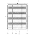
図1は本形態に係る光電変換装置10の平面図を示す。この光電変換装置10は、支持基板101上に固着された単結晶半導体層106に光が入射することで光電効果を発現する。単結晶半導体層106には、内蔵電界を形成するための不純物半導体層が形成されている。単結晶半導体層106としては、代表的には単結晶シリコンが適用される。また、単結晶半導体層106に代えて多結晶半導体層を適用することができる。この場合、多結晶シリコンが適用される。
FIG. 1 is a plan view of a
図1では、単結晶半導体層106の表面側に、網状の第2補助電極114が設けられ、裏面側に第1電極(平面図では表示されない)が設けられている。第1補助電極113は裏面に設けられる第1電極と接続する電極である。本形態の光電変換装置10は、絶縁表面を有する支持基板101に単結晶半導体層106が接着される構成なので、正極とそれに対する負極の電極は、支持基板101の同じ面に配設されている。
In FIG. 1, a net-like second
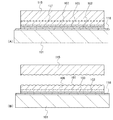
図1のA−B切断線に対応する光電変換装置10の断面構造を図2に示す。図2は、支持基板101に単結晶半導体層106が接合された光電変換装置を示す。支持基板101は絶縁表面を有する基板若しくは絶縁基板であり、例えば、アルミノシリケートガラス、アルミノホウケイ酸ガラス、バリウムホウケイ酸ガラスのような電子工業用に使われる各種ガラス基板が適用される。
FIG. 2 shows a cross-sectional structure of the
支持基板101と単結晶半導体層106の間には絶縁層102が設けられている。絶縁層102と単結晶半導体層106の間には第1電極103が設けられている。絶縁層102は支持基板101と接合しており、さらに第1電極103と密着していることにより、単結晶半導体層106が支持基板101上に固定される。絶縁層102は、支持基板101と接合するために、平滑面を有し親水性表面を有している絶縁膜で形成される。
An insulating
単結晶半導体層106は、代表的には単結晶シリコンが適用される。また、単結晶半導体層に代えて多結晶半導体層(代表的には多結晶シリコン)を適用することもできる。一導電型の第1不純物半導体層107と、一導電型とは逆の導電型の第2不純物半導体層108は、所定の元素を単結晶半導体層106に添加することにより形成される。第1不純物半導体層107をp型とする場合、第2不純物半導体層108はn型であり、その逆の選択も可能である。p型不純物元素としては硼素などの元素周期表第13族の元素が適用され、n型不純物元素としてはリン、砒素など元素周期表第15族の元素が適用される。不純物元素の添加は、イオン注入若しくはイオンドーピングで行うことができる。本明細書では、イオン注入とはイオン化したガスを質量分離して半導体に注入する方式を指し、イオンドーピングとはイオン化したガスを質量分離せず半導体に注入する方式をいう。
As the single
単結晶半導体層106に第1不純物半導体層107と第2不純物半導体層108を形成することにより内蔵電界が形成され、光照射により起電力を発生させることができる。すなわち、単結晶半導体層106に第1不純物半導体層107と第2不純物半導体層108でユニットセル(以下、第1ユニットセル104ともいう)を形成していることになる。なお、単結晶半導体層106にp型若しくはn型の単結晶半導体が適用される場合、第1不純物半導体層107は省略することが可能である。
By forming the first
単結晶半導体層106は単結晶半導体基板を薄片化して形成される。例えば、単結晶半導体基板として単結晶シリコンウエハを用い、所定の深さに水素イオンを高濃度に注入し、その後、熱処理を行って表層の単結晶シリコン層を分離する水素イオン注入分離法で単結晶半導体層106を形成する。また、ポーラスシリコン上に単結晶半導体をエピタキシャル成長させた後、ポーラスシリコン層をウオータージェットで劈開して分離する方法を適用しても良い。単結晶半導体基板として、代表的には単結晶シリコンウエハが適用される。単結晶半導体層106の厚さは0.1μm以上、10μm以下、好ましくは1μm以上5μm以下とする。単結晶半導体層106として単結晶シリコン半導体を適用する場合には、エネルギーギャップが1.12eVであり、間接遷移型の半導体であることから、太陽光を吸収するためにはこのような厚さが要求される。
The single
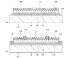
単結晶半導体層106の表面は凹凸構造を有している。この凹凸構造は、最大高低差(P−V)で300nm〜500nmの値を有している。なお、ここでいう山谷の最大高低差とは、山頂と谷底の高さの差を示す。また、ここでいう山頂と谷底とはJIS B0601で定義されている「山頂」「谷底」を三次元に拡張したものであり、山頂とは指定面の山において最も標高の高いところ、谷底とは指定面の谷において最も標高の低いところと表現される。この単結晶半導体層106の表面における凹凸構造は、酸素を含む雰囲気中でパルスレーザビームを照射することにより調整されている。
The surface of the single
第1電極103は、単結晶半導体層106の周辺端部領域で第1補助電極113と接触し、第2補助電極114は第2不純物半導体層108と接触している。この構成により、単結晶半導体層106の凹凸構造を有する面から光が入射することにより、第1電極103(第1補助電極113)と第2補助電極114の間に起電力が発生する。このとき、単結晶半導体層106の表面に凹凸構造があることにより光の反射が押さえられ、単結晶半導体層106に入射した光を閉じ込める効果を奏する。それにより、単結晶半導体層106の厚さが、0.1μm以上、10μm以下、好ましくは1μm以上5μm以下であっても入射光の光路長が実質的に増大し、光の吸収量を増やすことができる。すなわち、単結晶半導体層106に形成された凹凸構造は、光電変換装置10の変換効率を向上させる作用を奏する。
The
図3はタンデム型光電変換装置20を示す。図2で示す第1ユニットセル104上に第2ユニットセル105を積層したものである。第2ユニットセル105は、非単結晶半導体層109を用いて作製される。非単結晶半導体層109は、代表的には非晶質半導体である非晶質シリコンが適用される。また、非晶質シリコンに代えて非晶質シリコンゲルマニウムを適用してもよいし、非単結晶半導体層109に微結晶半導体層(代表的には微結晶シリコン)を適用することも可能である。一導電型の第3不純物半導体層110と、一導電型とは逆の導電型の第4不純物半導体層111は所定の不純物元素を含んで形成された非晶質半導体層又は微結晶半導体層で作製される。代表的には、所定の不純物元素を含んだ非晶質シリコン又は微結晶シリコンであり、その他、所定の不純物元素を含んだ非晶質シリコンカーバイトが適用される。第3不純物半導体層110をp型とする場合、第4不純物半導体層111はn型であり、その逆の選択も可能である。
FIG. 3 shows a tandem
非単結晶半導体層109は、半導体材料ガスを含む反応性ガスを電磁エネルギーにより分解して形成する。半導体材料ガスとしては、シラン若しくはジシランに代表されるシリコンの水素化物であり、その他シリコンのフッ化物又はシリコンの塩化物によるガスを用いる。このような半導体材料ガス、又は半導体材料ガスに水素、不活性ガスを混合して反応性ガスとして用いる。非単結晶半導体層109は、この反応性ガスを用い、電磁エネルギーとして、10MHzから200MHzの高周波電力を印加して薄膜の形成を行うプラズマCVD法により形成する。電磁エネルギーとしては、高周波電力に代えて1GHzから5GHz、代表的には2.45GHzのマイクロ波電力を印加しても良い。第3不純物半導体層110及び第4不純物半導体層111も同様にプラズマCVD法で形成されるものであり、前記した反応性ガスに、p型化する場合には不純物としてジボランを、n型化する場合には不純物としてフォスフィンを添加して成膜を行う。非単結晶半導体層109として、代表的には非晶質シリコン層が適用される。非単結晶半導体層109の厚さは50nm以上、300nm以下、好ましくは100nm以上、200nm以下とする。非単結晶半導体層109として非晶質シリコン半導体を適用する場合には、エネルギーギャップが1.75eVであり、この厚さにすることで、600nmよりも短い波長領域の光を吸収して光電変換することができる。
The non-single-
第2ユニットセル105の非単結晶半導体層109において、微結晶半導体層(代表的には微結晶シリコン層)を適用することもできる。微結晶半導体層を形成するために用いられる代表的な半導体材料ガスは、シラン(SiH4)であり、その他にもジシラン(Si2H6)が適用される。また、シラン(SiH4)にジクロロシラン(SiH2Cl2)、トリクロロシラン(SiHCl3)、テトラクロロシラン(SiCl4)、テトラフルオロシラン(SiF4)などを適宜混合して用いても良い。この半導体材料ガスを水素若しくはフッ素、水素若しくはフッ素とヘリウム、アルゴン、クリプトン、ネオンから選ばれた一種または複数種の希ガス元素で希釈して用いることで微結晶半導体層をプラズマCVD法で作製する。希釈率は10倍〜3000倍の範囲で半導体材料ガスを希釈することが好ましい。成膜は、概略0.1Pa〜133Paの減圧下で生成されるグロー放電プラズマで成膜が行われる。プラズマを形成するための電力は10MHzから200MHzの高周波電力又は、高周波電力に代えて1GHzから5GHz、代表的には2.45GHzのマイクロ波電力が印加される。また、半導体材料ガス中に、メタン(CH4)、エタン(C2H6)などの炭化物気体、ゲルマン(GeH4)、四フッ化ゲルマニウム(GeF4)などのゲルマニウム化気体を混入させて、エネルギーバンド幅を1.5〜2.4eV、若しくは0.9〜1.1eVに調節しても良い。微結晶半導体層は格子歪みを有し、該格子歪みにより光学特性が、単結晶シリコンの間接遷移型から直接遷移型に変化する。少なくとも10%の格子歪みにより、光学特性が直接遷移型に変化するが、局部的な歪みが存在することにより、直接遷移と間接遷移の混在した光学特性を呈する。微結晶シリコン層では、エネルギーギャップが概略1.45eVであり、単結晶シリコンよりもエネルギーギャップが広がるので、600nmよりも短い波長領域の光を吸収して光電変換することができる。
As the non-single-
本形態の光電変換装置は、第2電極112側から光を入射する構成である。第2電極112は、酸化インジウムスズ、酸化スズ、酸化亜鉛などの透明導電材料を用いて形成する。第1電極103は、チタン、モリブデン、タングステン、タンタル、クロム、ニッケルから選択された金属材料で形成する。また、第1電極103は、チタン、モリブデン、タングステン、タンタルの窒化物層を有し、該窒化物層が第1不純物半導体層107と接触する構成とする。半導体層と金属層の間に金属窒化物を介在させることにより、密着性を向上させることができる。
The photoelectric conversion device of this embodiment has a structure in which light is incident from the
第2ユニットセル105は、単結晶半導体層106の凹凸表面上に形成されることにより、その凹凸構造の影響を受けて、第2電極112の表面も凹凸化される。第2電極112の表面が凹凸化されていることにより、入射光の反射が低減する。すなわち、光入射側から下層に位置する単結晶半導体層106の凹凸構造と互いに作用しあって、第1ユニットセル104と第2ユニットセル105に光閉じ込め効果を発現させることができる。この効果により、タンデム型光電変換装置20の変換効率を向上させることができる。
When the
図4は、エネルギーギャップ1.12eVの単結晶半導体層106を有する第1ユニットセル104と、エネルギーギャップ1.75eVの非単結晶半導体層109を有する第2ユニットセル105を用いた場合のエネルギーバンド図を示す。光入射側にエネルギーギャップの広い非単結晶半導体層109を有する第2ユニットセル105が位置しており、その後方にエネルギーギャップの狭い単結晶半導体層106を有する第1ユニットセル104が配置している。なお、第1不純物半導体層107と第3不純物半導体層110はp型半導体、第2不純物半導体層108と第4不純物半導体層111はn型半導体の場合を示している。
FIG. 4 shows an energy band when a
図4のバンドモデル図で示すように光を吸収して励起された電子はn型半導体側に流れ、ホールはp型半導体側に流れる。その結果、第1ユニットセル104と第2ユニットセル105の接続部では、第1ユニットセル104側の電子及び第2ユニットセル側のホールがトラップされる形になる。この場合、第2不純物半導体層108と第3不純物半導体層110の接合界面に再結合中心が形成されるようにして、この接合界面で再結合電流が流れるようにする。第2不純物半導体層108は単結晶半導体であり、その上に第3不純物半導体層110として、非晶質半導体層又は微結晶半導体層をプラズマCVD法などで堆積することにより、接合界面で再結合電流が流れるような接合を形成することができる。
As shown in the band model diagram of FIG. 4, electrons excited by absorbing light flow to the n-type semiconductor side, and holes flow to the p-type semiconductor side. As a result, at the connection between the
図3のタンデム型の光電変換装置によれば、単結晶半導体層106で形成される第1ユニットセル104をボトムセルとして用いることで、800nm以上の長波長光の吸収をして光電変換することが可能となり、光電変換効率の向上に寄与する。この場合、単結晶半導体層106が10μm以下と薄層化されていることにより、光生成キャリアの再結合による損失を低減することができる。この場合において、光入射側から下層に位置する単結晶半導体層106の凹凸構造と互いに作用しあって、第1ユニットセル104と第2ユニットセル105に光閉じ込め効果を発現させることができる。この効果により、タンデム型光電変換装置20の変換効率を向上させることができる。
According to the tandem photoelectric conversion device in FIG. 3, by using the
(実施形態2)
次に、実施の形態1において示す図1のA−B切断線に対応する断面構造として、図2の場合を前提として光電変換装置10の製造方法について説明する。
(Embodiment 2)
Next, a manufacturing method of the
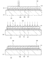
図5(A)に示す半導体基板115は円形の単結晶半導体基板より略四辺形に切り出されたものである。半導体基板115は、代表的には単結晶シリコンであって、表面が鏡面研磨されたものが好ましい。保護膜116は酸化シリコン又は窒化シリコンで形成することが好ましく化学気相成長法により形成する。
A
半導体基板115の一面に一導電型の第1不純物半導体層107を形成する。例えば、一導電型の不純物として硼素を添加して、第1不純物半導体層107をp型に形成する。第1不純物半導体層107は、本形態の光電変換装置において、光入射側と反対側の面に配置され、裏面電界(BSF:Back Surface Field)を形成する。硼素の添加は、ジボラン(B2H6)、三フッ化硼素(BF3)をソースガスとして、生成されたイオンを質量分離しないで電界で加速して、生成されるイオン流を基板に照射するイオンドーピング装置を用いて行う。
A one-conductivity-type first
図5(B)は、保護膜116を除去して、第1不純物半導体層107上に第1電極103を形成している。第1電極103は耐熱性金属で形成することが好ましい。耐熱性金属としては、チタン、モリブデン、タングステン、クロムなどの金属材料が適用される。これらの金属材料の窒化物を第1不純物半導体層107に接して形成し、さらに該金属層を積層して第1電極103を二層構造としても良い。金属窒化物を形成することで、第1電極103の密着性を向上させることができる。第1電極103は真空蒸着法又はスパッタリング法で形成する。
In FIG. 5B, the
図5(C)は、第1電極103が形成された面から、水素イオンを含むイオンビームを半導体基板115に照射して、損傷層117を形成する段階を示している。水素イオンは、好ましくはH3 +に代表されるようなクラスターイオンを打ち込んで、表面から一定の深さの領域に損傷層117を形成する。損傷層117の深さは、イオンの加速エネルギーによって制御される。損傷層117の深さにより半導体基板115から分離される単結晶半導体層の厚さが決まるので、クラスターイオンを加速する電界強度はそのことを考慮して決められる。損傷層117は半導体基板115の表面から10μm未満の深さ、すなわち50nm以上10000nm未満、好ましくは100nmから5000nmの深さに損傷層を形成することが好ましい。第1電極103を通してクラスターイオンを半導体基板115に打ち込むことで、イオンの照射により表面が損傷を受けてしまうことを防止することができる。
FIG. 5C shows a stage in which the damaged
水素イオンであるH3 +イオンに代表されるようなクラスターイオンの注入は、水素プラズマを生成し、該プラズマ中に生成されるイオンを質量分離せず、そのまま電界で加速することにより注入するイオンドーピング装置を用いて行うことができる。イオンドーピング装置を用いることにより、面積の大きい半導体基板115に対しても容易に行うことができる。
Cluster ions such as H 3 + ions, which are hydrogen ions, are implanted by generating a hydrogen plasma and accelerating it in an electric field without mass separation of the ions generated in the plasma. This can be performed using a doping apparatus. By using an ion doping apparatus, the
図9は、イオンドーピング装置の構成を示す。イオン源200では質量の異なる複数種のイオンが生成される。イオン源200にはガス供給部204から水素等の所定のガスが供給される。イオン源200に水素等が導入された後、イオン源200のフィラメント201に電圧を印加してアーク放電を発生させる。これにより、水素がイオン化して、質量の異なる複数種のイオンが生成される。
FIG. 9 shows the configuration of an ion doping apparatus. The
イオン源200で生成されたイオンは、引出し電極系205によってイオンビームを形成する。イオンビームは載置台206に置かれた半導体基板115に照射される。イオンビームに含まれるイオン種の割合は載置台206の近傍に設けられた質量分析管207によって計量される。質量分析管207によって計数されたイオン密度は質量分析計208で信号変換され、その結果を電源制御部203にフィードバックさせるようにしても良い。電源制御部203はイオン密度の計数結果に従って、フィラメント電源202を制御することができる。
Ions generated by the
ガス供給部204から供給された水素等のガスは、イオンドーピング装置のチャンバー内を流れる。イオン源200に供給された水素は、式(1)の反応によりイオン化する。
H2+e− → H2 ++2e− −Q (Q=15.39eV) (1)
A gas such as hydrogen supplied from the
H 2 + e − → H 2 + + 2e − −Q (Q = 15.39 eV) (1)
イオンドーピング装置のチャンバー内の圧力は1×10⁻²Paから1×10⁻¹Paであり、電離度があまり高くないことからH2 +イオンより原料ガスであるH2が多く存在している。従って、イオン源で生成されたH2 +イオンは、引出し電極系205で引き出されるまでにH2と反応し、式(2)の反応が起こる。
H2 ++H2 → H3 ++H +Q (Q=1.49eV) (2)
The pressure in the chamber of the ion doping apparatus is 1 × 10 −2 Pa to 1 × 10 −1 Pa, and since the degree of ionization is not so high, there is more H 2 as a source gas than H 2 + ions. . Therefore, H 2 + ions generated in the ion source react with H 2 before being extracted by the
H 2 + + H 2 → H 3 + + H + Q (Q = 1.49 eV) (2)
H3 +は、H+及びH2 +よりも安定な分子として存在するため、H2と衝突する割合が高ければH3 +が多量に生成されることになる。このことは、質量分析管207を用いて載置台206に照射されるイオンビームの質量分析結果を見れば明らかである。イオン種H+、H2 +、H3 +の総量に対してH3 +イオンの割合は70%以上となっている。それにより、クラスターイオンであるH3 +を多量に発生させたイオンビームを基板に照射することで、H+、H2 +を注入するよりも水素原子の注入効率が向上し、ドーズ量が少なくても水素を半導体基板115に高濃度に注入することができる。
Since H 3 + exists as a more stable molecule than H + and H 2 +, if the ratio of collision with H 2 is high, a large amount of H 3 + is generated. This is apparent from the mass analysis result of the ion beam irradiated to the mounting table 206 using the
クラスターイオンとしてH3 +の割合を高めておくことで、損傷層117には1×10²⁰atoms/cm3以上の水素を含ませることが可能である。半導体基板115に形成される損傷層117は結晶構造が失われ微小な空孔が形成され、多孔質構造となっている。そのため、比較的低温(600℃以下)の熱処理によって損傷層117に形成された微小な空洞の体積変化が起こり、損傷層117に沿って単結晶半導体層を分離することができる。
By increasing the ratio of H 3 + as cluster ions, the damaged
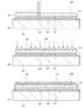
図5(D)は、第1電極103上に絶縁層102を形成する段階を示す。絶縁層102は、酸化シリコン、酸化窒化シリコン、窒化酸化シリコン、窒化シリコンなどの絶縁膜で形成する。絶縁層102は平滑で親水性の表面を有するものであれば良い。絶縁層102の平滑性でいえば、平均面粗さRa値が1nm以下、好ましくは0.5nm以下であることが好ましい。なお、ここでいう平均面粗さとは、JIS B0601で定義されている中心線平均粗さを面に対して適用できるよう三次元に拡張したものである。
FIG. 5D illustrates a step of forming the insulating
平滑面を有し親水性表面を形成できる絶縁層としては、水素を含有する酸化シリコン、水素を含有する窒化シリコン、酸素と水素を含有する窒化シリコン、水素を含有する酸化窒化シリコン、水素を含有する窒化酸化シリコン等を適用することができる。 As an insulating layer having a smooth surface and capable of forming a hydrophilic surface, silicon oxide containing hydrogen, silicon nitride containing hydrogen, silicon nitride containing oxygen and hydrogen, silicon oxynitride containing hydrogen, containing hydrogen Silicon nitride oxide or the like can be applied.
なお、酸化窒化シリコン膜とは、その組成として、窒素よりも酸素の含有量が多いものであって、濃度範囲として酸素が55〜65原子%、窒素が0.5〜20原子%、シリコンが25〜35原子%、水素が0.1〜10原子%の範囲で含まれるものをいう。また、窒化酸化シリコン膜とは、その組成として、酸素よりも窒素の含有量が多いものであって、濃度範囲として酸素が15〜30原子%、窒素が20〜50原子%、シリコンが25〜35原子%、水素が15〜25原子%の範囲で含まれるものをいう。 Note that the silicon oxynitride film has a composition with a higher oxygen content than nitrogen, and the concentration range is oxygen of 55 to 65 atomic%, nitrogen of 0.5 to 20 atomic%, and silicon. 25 to 35 atomic%, and hydrogen is included in the range of 0.1 to 10 atomic%. The silicon nitride oxide film has a composition containing more nitrogen than oxygen, and the concentration ranges of oxygen are 15 to 30 atomic%, nitrogen is 20 to 50 atomic%, and silicon is 25 to 25%. 35 atomic% and hydrogen are included in the range of 15 to 25 atomic%.
水素を含有する酸化シリコンとしては、例えば有機シランを用いた化学気相成長法により作製される酸化シリコンが好ましい。有機シランを用いて形成された絶縁層102として、酸化シリコン膜を用いることによって、支持基板と転置用半導体層との接合を強固にすることができるためである。有機シランとしては、テトラエトキシシラン(TEOS:化学式Si(OC2H5)4)、テトラメチルシラン(TMS:化学式Si(CH3)4)、テトラメチルシクロテトラシロキサン(TMCTS)、オクタメチルシクロテトラシロキサン(OMCTS)、ヘキサメチルジシラザン(HMDS)、トリエトキシシラン(SiH(OC2H5)3)、トリスジメチルアミノシラン(SiH(N(CH3)2)3)等のシリコン含有化合物を用いることができる。
As the silicon oxide containing hydrogen, for example, silicon oxide produced by a chemical vapor deposition method using organosilane is preferable. This is because by using a silicon oxide film as the insulating
水素を含有する窒化シリコンは、シランガスとアンモニアガスを用いたプラズマCVD法により作製することができる。前記ガスに水素が加えられていても良い。酸素と水素を含有する窒化シリコンは、シランガスとアンモニアガスと亜酸化窒素ガスを用いたプラズマCVD法で作製することができる。いずれにしても、プラズマCVD法、減圧CVD法、常圧CVD法等の化学気相成長法により、シランガス等を原料ガスとして用いて作製される酸化シリコン、酸化窒化シリコン、窒化酸化シリコンであって水素が含まれるものであれば適用することができる。絶縁層102の成膜温度は、単結晶半導体基板に形成した損傷層117から水素が脱離しない温度として、350℃以下の成膜温度が推奨される。
Silicon nitride containing hydrogen can be manufactured by a plasma CVD method using silane gas and ammonia gas. Hydrogen may be added to the gas. Silicon nitride containing oxygen and hydrogen can be manufactured by a plasma CVD method using silane gas, ammonia gas, and nitrous oxide gas. In any case, silicon oxide, silicon oxynitride, and silicon nitride oxide produced by using a silane gas or the like as a source gas by a chemical vapor deposition method such as a plasma CVD method, a low pressure CVD method, or an atmospheric pressure CVD method. Any material containing hydrogen can be used. As the deposition temperature of the insulating
図6(A)は支持基板101と半導体基板115とを接着する段階を示す。この接着は、平滑であり親水性表面を有する絶縁層102が支持基板101に密着することによりなされる。この接合は、水素結合やファン・デル・ワールス力が作用している。接合は、半導体基板115及び支持基板101の表面の水酸基や水分子が接着剤として働くことによって起きる。熱処理によって、水分子が拡散し、残留成分のシラノール基(Si−OH)同士が水素結合で結合する。さらにこの接合部は、水素が抜けることでシロキサン結合(Si−O−Si)が形成されることで共有結合になり、半導体基板115と支持基板101の接合が強固なものとなる。なお、支持基板101の接着面にも、バリア層118として窒化シリコン膜、窒化酸化シリコン膜などを形成しておいても良い。バリア層118を形成することで、支持基板101からの不純物汚染を防止することができる。
FIG. 6A shows a step of bonding the
図6(B)は、加熱処理により損傷層117を劈開して半導体基板115を支持基板101から分離する段階を示す。加熱処理の温度は絶縁層102の成膜温度以上、支持基板101の耐熱温度以下で行うことが好ましい。例えば400℃から600℃の加熱処理を行うことにより、損傷層117に形成された微小な空洞の堆積変化が起こり、その領域に沿って劈開する。絶縁層102は支持基板101と接着しているので、支持基板101には単結晶半導体層106と第1電極103が残存する。このとき、単結晶半導体層106の厚さは、損傷層の深さにほぼ対応し、50nm以上10000nm未満、好ましくは100nmから5000nmの厚さに形成される。以上の工程により、支持基板101上に絶縁層102により固定された単結晶半導体層106を設けることができる。
FIG. 6B shows a step of cleaving the damaged
図7(A)は、結晶欠陥の残留する単結晶半導体層106の修復と、表面に凹凸構造を形成するために、単結晶半導体層106の劈開面にレーザ処理をする段階を示している。レーザビームを単結晶半導体層106の劈開面に照射することで、単結晶半導体層106の少なくとも劈開面側は溶融し固相状態の下層部を種結晶として、その後の冷却過程で再単結晶化する。その過程で単結晶半導体層106の表面を凹凸化させることができる。
FIG. 7A illustrates a stage in which laser treatment is performed on a cleavage plane of the single
このレーザ処理は酸素を含む雰囲気中で、パルスレーザビームを単結晶半導体層106の劈開面に照射することにより行われる。このレーザ処理のとき、少なくともレーザビームの照射領域は、250℃から600℃の温度に加熱されていることが好ましい。照射領域を加熱しておくことで、レーザビームの照射による溶融時間を長くすることができ、表面の凹凸化と同時に結晶欠陥の修復を効果的に行うことができる。レーザビームは単結晶半導体層106の劈開面側を溶融させるものの、支持基板101は殆ど加熱されないので、ガラス基板のような耐熱性の低い支持基板を用いることが可能になる。また、第1電極103は耐熱性金属で形成されているので、上記温度で加熱されても単結晶半導体層106に悪影響を及ぼすことがない。当該耐熱性金属と第1不純物半導体層107の界面ではシリサイドが形成され、より電流が流れ易くなる。
This laser treatment is performed by irradiating the cleaved surface of the single
単結晶半導体層106の表面を凹凸化させるレーザ処理は、窒素又はアルゴンに代表される不活性気体に酸素が0.1体積%から25体積%含まれる雰囲気中で行う。また、窒素又はアルゴンに代表される不活性気体に酸素若しくは酸化物気体が0.1体積%から50体積%含まれる雰囲気中で行ってもよい。酸化物気体としては、二酸化炭素、亜酸化窒素などが適用可能である。その他、上記雰囲気に代えて、空気中、好ましくは乾燥空気中で行っても良い。
The laser treatment for roughening the surface of the single
パルスレーザビームは、光源(レーザ発振器)として、エキシマレーザ(XeCl(308nm)、KrF(248nm)、ArF(193nm))、YAG、YVO4レーザに代表される固体レーザ(第2高調波(532nm)、第3高調波(355nm)第4高調波(266nm))を用いる。例えば、波長308nmのエキシマレーザビームを照射する場合には、発振周波数5〜50Hz、エネルギー密度100〜500mJ/cm2、線状ビームのオーバーラップ割合を80〜98%として、単結晶半導体層106を処理する。
The pulse laser beam is a solid-state laser (second harmonic (532 nm)) typified by an excimer laser (XeCl (308 nm), KrF (248 nm), ArF (193 nm)), YAG, YVO 4 laser as a light source (laser oscillator). , Third harmonic (355 nm), fourth harmonic (266 nm)). For example, in the case of irradiating an excimer laser beam with a wavelength of 308 nm, the single
また、パルスレーザビームの波長と照射回数を制御することにより、規則性のある凹凸構造を単結晶半導体層106の表面に形成することができる。例えば、波長308nmのエキシマレーザビームを、350mJ/cm2〜450mJ/cm2として、同じ領域に、パルス幅10nsec〜30nsecで繰り返し周波数が10Hz〜50Hzのパルスレーザビームを20回〜50回照射することで、凸部が格子状に整列した凹凸構造を形成することができる。この凸部の整列間隔は照射するパルスレーザビームの波長を選択することによって制御することができる。例えば、波長308nmのエキシマレーザを照射することで、凸部のピッチを概ね308nmとすることができる。また、波長527nmのYLFレーザを用いると凸部のピッチは概ね527nmとなり、Nd:YAGレーザの第2高調波(発振波長:532nm)を用いると凸部のピッチは概ね532nmとすることができる。
In addition, a regular uneven structure can be formed on the surface of the single
レーザ処理を行うためのレーザ処理装置の一例を図10を参照して説明する。レーザ処理装置は、レーザ発振器210、レーザ光を細い線状ビームに集光伸張させる光学系211、レーザ照射領域の雰囲気を制御するガス噴射筒212、該ガス噴射筒212に雰囲気制御ガスを供給するガス供給部213、流量制御部214、ガス加熱部215、支持基板101を浮遊させ搬送する基板ステージ222、基板の両端を支持して搬送するガイドレール223、基板ステージ222に浮遊用にガスを供給するガス供給部216を備えている。
An example of a laser processing apparatus for performing laser processing will be described with reference to FIG. The laser processing apparatus includes a
レーザ発振器210は、その発振波長が、紫外光域乃至可視光域にあるものが選択される。レーザ発振器210は、パルス発振型のArF、KrF又はXeClエキシマレーザ、或いはNd:YAGレーザ、YLFレーザなどの固体レーザで、繰り返し周波数1MHz以下、パルス幅10n秒以上500n秒以下のものが好ましい。例えば、繰り返し周波数10Hz〜300Hz、パルス幅10〜30nsec、波長308nmのXeClエキシマレーザを用いる。
As the
光学系211はレーザ光を集光及び伸張して、被照射面に断面形状が線状となるレーザビームを形成する。線状ビームを形成する光学系211は、シリンドリカルレンズアレイ217、シリンドリカルレンズ218、ミラー219、ダブレットシリンドリカルレンズ220により構成される。レンズの大きさにもよるが、長手方向は100mm〜700mm、短手方向は100μm〜500μm程度の線状レーザ光を照射することが可能である。
The
線状に集光されたレーザビームはガス噴射筒212の光導入窓221を通して支持基板101に照射される。ガス噴射筒212は支持基板101と近接して配置されている。ガス噴射筒212にはガス供給部213から窒素等の不活性ガスと酸素を含むガスが供給されている。当該ガスはガス噴射筒212の支持基板101に面した開口部から噴出する。ガス噴射筒212の開口部は、光導入窓221から入射したレーザビームが支持基板101に照射されるように、線状レーザビームの光軸に合わせて配置されている。ガス噴射筒212の開口部から噴射する酸化性気体により、レーザビームの照射領域の雰囲気制御を行う。
The laser beam condensed linearly is applied to the
ガス噴射筒212に供給する窒素等の不活性ガスと酸素を含むガスは、ガス加熱部215を250℃から700℃に制御することにより、支持基板101のレーザビームの照射面の温度を100℃から600℃に制御でき、上記のようにレーザビームの照射による溶融時間を制御することができる。
An inert gas such as nitrogen and a gas containing oxygen to be supplied to the
基板ステージ222には、ガス供給部216から空気又は窒素が流量制御部214を通して供給される。ガス供給部216から供給される気体は、基板ステージ222の上面から、支持基板101の下面を吹き付けるように噴出させて、該支持基板101を浮遊させる。支持基板101は両端がガイドレール223上を動くスライダ224に載せられて搬送されるが、基板ステージ222側からガスが吹き付けられることにより、湾曲せずに浮遊した状態で搬送することができる。本形態のレーザ処理装置では、支持基板101の上面にガス噴射筒212から窒素ガスが噴出するので、その裏側からもガスを吹き付けることにより、支持基板101の撓みを防ぐことができる。このような基板ステージ222の構成は、一辺が500mmを超え、厚さが1mm以下の支持基板を処理する場合に有効である。例えば、600mm×720mm乃至730mm×920mmで厚さが0.7mm以下の支持基板を処理することができる。
Air or nitrogen is supplied to the
基板ステージ222は、レーザ照射部近傍と、それ以外の領域に区画されていても良い。基板ステージ222のレーザ照射部近傍では、ガス加熱部215により加熱された窒素ガスを吹き付けるようにしても良い。それにより、支持基板101を加熱することができる。
The
なお、図10で示すレーザ処理装置は一例であり、レーザビーム照射時の雰囲気を窒素等の不活性ガスと酸素を含む雰囲気に制御できるものであれば他の構成を適用することもできる。例えば、レーザビームを導入可能な窓を備えた密閉可能な処理室に支持基板を保持し、該処理室に窒素等の不活性ガスと酸素を含むガスを導入して雰囲気制御しても良い。 Note that the laser processing apparatus illustrated in FIG. 10 is an example, and any other structure can be applied as long as the atmosphere at the time of laser beam irradiation can be controlled to an atmosphere containing an inert gas such as nitrogen and oxygen. For example, the support substrate may be held in a sealable processing chamber provided with a window capable of introducing a laser beam, and the atmosphere may be controlled by introducing an inert gas such as nitrogen and a gas containing oxygen into the processing chamber.
図7(B)は、単結晶半導体層106に第1不純物半導体層107とは逆の導電型の不純物元素を添加して、第2不純物半導体層108を形成する。例えば、リン又は砒素を添加して第2不純物半導体層108をn型に形成する。この場合、先の工程でレーザ処理により表面の結晶欠陥が修復されているので、第2不純物半導体層108の不純物濃度を精密に制御することができる。すなわち、レーザビームを照射して、単結晶半導体層の表面を処理し、その後、不純物領域を形成することにより、不純物濃度を高濃度化することができ、浅い接合を形成することができる。それにより、光生成キャリアの収集効率の高い光電変換装置を得ることができる。
In FIG. 7B, a second
図7(C)は、単結晶半導体層106の端部をエッチングして第1電極103を露出させる段階を示している。エッチングは単結晶半導体層106にマスクを形成し、三フッ化窒素(NF3)、六フッ化硫黄(SF6)などのガスを用いてドライエッチングを行う。
FIG. 7C illustrates a step in which the end portion of the single
図8(A)は、第1電極103に接する第1補助電極113と、第2不純物半導体層108上の第2補助電極114を形成する段階を示している。第1補助電極113は図7(C)でエッチングにより露出した第1電極103に接触するように形成する。第2補助電極114は、図1の平面図で示すように櫛型又は格子状の電極である。第1補助電極113及び第2補助電極114は、アルミニウム、銀、鉛錫(半田)などで形成すれば良い。例えば、銀ペーストを用いてスクリーン印刷法で形成する。
FIG. 8A shows a stage in which the first
その後、図8(B)で示すように、パッシベーション膜を兼ねた反射防止膜119を形成する。反射防止膜119は、窒化シリコン膜で形成することが好ましく、窒化シリコンと窒化酸化シリコンの積層膜で形成しても良い。
After that, as shown in FIG. 8B, an
このようにして図1で示す光電変換装置10を製造することができる。本工程によれば、異種材料間の接合技術と、レーザ処理技術を用いることにより、700℃以下(好適には500℃以下)のプロセス温度で10μm以下の単結晶半導体層を有する光電変換装置を製造することができる。すなわち、耐熱温度が700℃以上の大面積ガラス基板に、単結晶半導体層を設けた光電変換装置を製造することができる。単結晶半導体層は単結晶半導体基板の表層を分離することにより得られるが、当該単結晶半導体基板は繰り返し利用することができるので資源を有効に利用することができる。なお、同様の工程により第2ユニットセルを作製することで、図3に示すタンデム型光電変換装置を製造することができる。
In this way, the
(実施形態3)
本形態は、実施形態2と異なる製造工程を図11に示す。図11において、(A)保護膜116を形成して第1不純物半導体層107を半導体基板115の一面に形成した後、(B)保護膜116をそのまま残して損傷層117を形成する。その後、(C)保護膜116を除去して第1電極103を形成する。本形態の工程によれば保護膜116を有効に利用することができる。すなわち、保護膜116を損傷層117形成後に除去することで、半導体基板115の表面の接合表面を平坦なものとすることができる。保護膜116は50nmから200nmの厚さで設けることが好ましい。また、第1不純物半導体層107を通して水素のクラスターイオンが打ち込まれる損傷層117を形成することにより、第1不純物半導体層107の水素化を兼ねることができる。
(Embodiment 3)
This embodiment shows a manufacturing process different from that in Embodiment 2 in FIG. In FIG. 11, (A) a
(実施形態4)
本形態は、実施形態2と異なる製造工程を図12に示す。図12において、(A)半導体基板115の一面に第1電極103を形成し、(B)第1電極103を通して一導電型の不純物元素を添加して第1不純物半導体層107を形成する。そして、(C)第1電極103を通して水素のクラスターイオンを打ち込み損傷層117を形成する。本工程では、第1電極103の形成後にイオンドーピングを行うことにより、第1電極103をイオンドーピングにおける損傷防止層として利用することができる。それによりイオンドーピングのために保護膜を形成する工程を省略することができる。
(Embodiment 4)
In this embodiment, a manufacturing process different from that in Embodiment 2 is shown in FIG. In FIG. 12, (A) a
(実施形態5)
本形態は、実施形態2と異なる製造工程を図13に示す。図13において、(A)半導体基板115の一面に第1電極103を形成し、(B)第1電極103を通して水素のクラスターイオンを打ち込み損傷層117を形成する。そして、(C)第1電極103を通して一導電型の不純物元素を添加して第1不純物半導体層107を形成する。本工程では、第1電極103を最初に形成することにより、第1電極103をイオンドーピングにおける損傷防止層として利用することができる。本形態では、イオンドーピングのために保護膜を形成する工程を省略することができる。
(Embodiment 5)
This embodiment shows a manufacturing process different from that in Embodiment 2 in FIG. In FIG. 13, (A) a
(実施形態6)
本形態は、実施形態2と異なる製造工程を図14に示す。図14において、(A)保護膜116を形成して水素のクラスターイオンを半導体基板115の一面に打ち込んで損傷層117を形成し、(B)保護膜116をそのまま残して第1不純物半導体層107を形成する。そして、(C)保護膜116を除去して第1電極103を形成する。本工程は保護膜116をイオンドーピング時の損傷防止膜として、さらに第1不純物半導体層107を形成するときのドーピング深さを調節する膜として有効に利用している。また、損傷層117を形成した後に、第1不純物半導体層107を形成することにより、該第1不純物半導体層107の不純物濃度を高濃度化することができ、浅い接合を形成することができる。それにより、裏面電界(BSF:Back Surface Field)効果を発現させ、光生成キャリアの収集効率を高めることができる。
(Embodiment 6)
This embodiment shows a manufacturing process different from that in Embodiment 2 in FIG. In FIG. 14, (A) a
(実施形態7)
本形態は、実施形態2と異なる製造工程を図15に示す。図15において、(A)保護膜116を形成して水素のクラスターイオンを打ち込み損傷層117を形成し、(B)保護膜116を除去して第1電極103を形成する。そして、(C)第1電極103を通して一導電型の不純物元素を添加して第1不純物半導体層107を形成する。第1電極103を通して第1不純物半導体層107を形成することにより、第1不純物半導体層107の厚さを制御することが容易となる。
(Embodiment 7)
In this embodiment, a manufacturing process different from that in Embodiment 2 is shown in FIG. In FIG. 15, (A) a
(実施形態8)
本形態は、実施形態2と異なる製造工程を図16に示す。支持基板101上に単結晶半導体層106を接着し(図6(B))、図16(A)で示すように結晶欠陥の残留する単結晶半導体層106の修復と、表面に凹凸構造を形成するレーザ処理を行う。そして図16(B)で示すように、単結晶半導体層106に第1不純物半導体層107とは逆の導電型の不純物元素を添加して第2不純物半導体層108を形成する。その後、図16(C)に示すように第2不純物半導体層108上に反射防止膜119を形成する。
(Embodiment 8)
This embodiment shows a manufacturing process different from that in Embodiment 2 in FIG. The single
その後、図17(A)で示すように、単結晶半導体層106の端部をエッチングして第1電極103を露出させ、図17(B)で示すように第1補助電極113及び第2補助電極114を形成する。第2補助電極114は反射防止膜119上に形成し、その後、絶縁破壊電圧を瞬間的に印加することにより第2不純物半導体層108と導通をとることができ、補助電極として機能させることができる。
After that, as shown in FIG. 17A, the end portion of the single
本形態によれば、単結晶半導体層106に第2不純物半導体層108を形成した後にパッシベーション膜としても機能する反射防止膜119を形成することで、表面再結合速度を低くすることができ、光電変換装置の変換効率を高めることができる。
According to this embodiment, by forming the
本形態は、実施形態2〜7と自由に組み合わせることができる。 This embodiment can be freely combined with Embodiments 2 to 7.
(実施形態9)
本形態は、実施形態2と異なる製造工程を図18に示す。支持基板101上に単結晶半導体層106を接着した後(図6(B))、図18(A)において示すように、結晶欠陥の残留する単結晶半導体層106の修復と、表面に凹凸構造を形成するレーザ処理を行う。その後、図18(B)で示すように反射防止膜119を形成し、図18(C)で示すように第2不純物半導体層108を形成する。本形態によれば、第2不純物半導体層108の形成前にレーザ処理を行うので、レーザビームの照射による溶融領域を単結晶半導体層106の内部まで広げることができ、再単結晶化による欠陥修復の効果をより高めることができる。
(Embodiment 9)
In this embodiment, a manufacturing process different from that in Embodiment 2 is shown in FIG. After the single
その後、図7(C)のように単結晶半導体層106の周辺部をエッチングして第1電極103を露出させ、第1補助電極113及び第2補助電極114を形成すれば良い。第2補助電極114は反射防止膜119上に形成されるが、絶縁破壊電圧を瞬間的に印加してバーンインコンタクトを形成することにより電極として機能させることができる。
After that, the first
本形態は、実施形態2〜7と自由に組み合わせることができる。 This embodiment can be freely combined with Embodiments 2 to 7.
(実施形態10)
本形態は、実施形態2と異なる製造工程を図19に示す。支持基板101上の単結晶半導体層106にレーザ処理を行い、再単結晶化と表面に凹凸構造を形成する。そして図19(A)で示すように、単結晶半導体層106を覆うように絶縁層120を形成する。そして、図19(B)で示すように、絶縁層120に開口部を形成して単結晶半導体層106を露出させ、その開口部に第2不純物半導体層108を形成する。その後、図19(C)で示すように、絶縁層120と単結晶半導体層106を貫通し第1電極103に達する開口部を形成し、第1補助電極113及び第2補助電極114を形成する。さらに反射防止膜119を形成する。本形態のように、単結晶半導体層106の内側に開口部を形成して第1電極103と導通する第1補助電極113を形成することにより、光電変換装置の小型化を図ることができる。
(Embodiment 10)
This embodiment shows a manufacturing process different from that in Embodiment 2 in FIG. The single
本形態は、実施形態2〜7と自由に組み合わせることができる。 This embodiment can be freely combined with Embodiments 2 to 7.
(実施形態11)
実施形態1〜10により製造される光電変換装置を用いた太陽光発電モジュールの一例を図20(A)に示す。この太陽光発電モジュール30は、支持基板101に設けられた単結晶半導体層106により光電変換装置10が構成されている。単結晶半導体層106には光電変換機能を発現させる第1不純物半導体層、第2不純物半導体層などが形成されている。
(Embodiment 11)
An example of a photovoltaic power generation module using the photoelectric conversion device manufactured according to
第1補助電極113は単結晶半導体層106の裏面側に形成されている第1電極と接続する電極であり、第2補助電極114は櫛形又は格子状の電極である。第1補助電極113と第2補助電極114は支持基板101の一面に形成され、支持基板101の端部領域でコネクタ用の第1裏面電極121と第2裏面電極122とそれぞれ接続する。図20(B)は、C−D切断線に対応する断面図であり、支持基板101の貫通口を通して第1補助電極113と第2補助電極114が第1裏面電極121と第2裏面電極122とそれぞれ接続している。
The first
このように、支持基板101に単結晶半導体層106を接合して光電変換装置10を形成することにより、太陽光発電モジュールの薄型化を図ることができる。なお、本形態において、光電変換装置10に代えて、図3で示すタンデム型光電変換装置20を適用しても良い。
In this manner, the photovoltaic module can be thinned by bonding the single
(実施形態12)
図21は太陽光発電モジュール30を用いた太陽光発電システムの一例を示す。一又は複数の太陽光発電モジュール30の出力電力は、充電制御回路123により蓄電池124を充電する。蓄電池124の充電量が多い場合には、負荷125に直接出力される場合もある。
Embodiment 12
FIG. 21 shows an example of a solar power generation system using the solar
蓄電池124として電気二重層キャパシタを用いると、充電に化学反応を必要とせず、急速に充電することができる。また、化学反応を利用する鉛蓄電池などに比べ、寿命を約8倍、充放電効率を1.5倍に高めることができる。負荷125としては、蛍光灯、発光ダイオード、エレクトロルミネッセンスパネルなどの照明、小型の電子機器など、さまざまな用途に応用することができる。
When an electric double layer capacitor is used as the
10 光電変換装置
20 タンデム型光電変換装置
30 太陽光発電モジュール
101 支持基板
102 絶縁層
103 第1電極
104 第1ユニットセル
105 第2ユニットセル
106 単結晶半導体層
107 第1不純物半導体層
108 第2不純物半導体層
109 非単結晶半導体層
110 第3不純物半導体層
111 第4不純物半導体層
112 第2電極
113 第1補助電極
114 第2補助電極
115 半導体基板
116 保護膜
117 損傷層
118 バリア層
119 反射防止膜
120 絶縁層
121 第1裏面電極
122 第2裏面電極
123 充電制御回路
124 蓄電池
125 負荷
200 イオン源
201 フィラメント
202 フィラメント電源
203 電源制御部
204 ガス供給部
205 引出し電極系
206 載置台
207 質量分析管
208 質量分析計
210 レーザ発振器
211 光学系
212 ガス噴射筒
213 ガス供給部
214 流量制御部
215 ガス加熱部
216 ガス供給部
217 シリンドリカルレンズアレイ
218 シリンドリカルレンズ
219 ミラー
220 ダブレットシリンドリカルレンズ
221 光導入窓
222 基板ステージ
223 ガイドレール
224 スライダ
DESCRIPTION OF
Claims (6)
前記電極を通して、前記単結晶半導体基板に、一導電型を付与する不純物元素を添加して第1不純物半導体層を形成し、
前記電極を通して、前記単結晶半導体基板に、質量が水素分子よりも重い水素のクラスターイオンを70%以上含むイオンビームを注入して損傷層を形成し、
前記電極に接する絶縁層を形成し、
支持基板と、前記単結晶半導体基板の前記絶縁層とを接着し、
熱処理を行って、前記損傷層を劈開させることにより、前記単結晶半導体基板から単結晶半導体層を分離し、前記支持基板上に前記単結晶半導体層を残存させたまま前記単結晶半導体基板を除去し、
不活性気体及び酸素を含む雰囲気中で、前記単結晶半導体層の劈開面にパルスレーザビームを照射して、前記単結晶半導体層の表面を凹凸化し、
前記単結晶半導体層の劈開面側に、前記一導電型とは逆の導電型を付与する不純物元素を添加して第2不純物半導体層を形成することを特徴とする光電変換装置の製造方法。 An electrode is formed on one surface of a single crystal semiconductor substrate,
An impurity element imparting one conductivity type is added to the single crystal semiconductor substrate through the electrode to form a first impurity semiconductor layer,
Through the electrode, an ion beam containing 70% or more of hydrogen cluster ions whose mass is heavier than hydrogen molecules is implanted into the single crystal semiconductor substrate to form a damaged layer,
Forming an insulating layer in contact with the electrode;
Bonding the support substrate and the insulating layer of the single crystal semiconductor substrate,
By performing a heat treatment to cleave the damaged layer, the single crystal semiconductor layer is separated from the single crystal semiconductor substrate, and the single crystal semiconductor substrate is removed while the single crystal semiconductor layer remains on the supporting substrate. And
Irradiating the cleaved surface of the single crystal semiconductor layer with a pulsed laser beam in an atmosphere containing an inert gas and oxygen, the surface of the single crystal semiconductor layer is made uneven,
A method for manufacturing a photoelectric conversion device, wherein an impurity element imparting a conductivity type opposite to the one conductivity type is added to a cleavage plane side of the single crystal semiconductor layer to form a second impurity semiconductor layer.
前記電極を通して、前記単結晶半導体基板に、質量が水素分子よりも重い水素のクラスターイオンを70%以上含むイオンビームを注入して損傷層を形成し、
前記電極を通して、前記単結晶半導体基板に、一導電型を付与する不純物元素を添加して第1不純物半導体層を形成し、
前記電極に接する絶縁層を形成し、
支持基板と、前記単結晶半導体基板の前記絶縁層とを接着し、
熱処理を行って、前記損傷層を劈開させることにより、前記単結晶半導体基板から単結晶半導体層を分離し、前記支持基板上に前記単結晶半導体層を残存させたまま前記単結晶半導体基板を除去し、
不活性気体及び酸素を含む雰囲気中で、前記単結晶半導体層の劈開面にパルスレーザビームを照射して、前記単結晶半導体層の表面を凹凸化し、
前記単結晶半導体層の劈開面側に、前記一導電型とは逆の導電型を付与する不純物元素を添加して第2不純物半導体層を形成することを特徴とする光電変換装置の製造方法。 An electrode is formed on one surface of a single crystal semiconductor substrate,
Through the electrode, an ion beam containing 70% or more of hydrogen cluster ions whose mass is heavier than hydrogen molecules is implanted into the single crystal semiconductor substrate to form a damaged layer,
An impurity element imparting one conductivity type is added to the single crystal semiconductor substrate through the electrode to form a first impurity semiconductor layer,
Forming an insulating layer in contact with the electrode;
Bonding the support substrate and the insulating layer of the single crystal semiconductor substrate,
By performing a heat treatment to cleave the damaged layer, the single crystal semiconductor layer is separated from the single crystal semiconductor substrate, and the single crystal semiconductor substrate is removed while the single crystal semiconductor layer remains on the supporting substrate. And
Irradiating the cleaved surface of the single crystal semiconductor layer with a pulsed laser beam in an atmosphere containing an inert gas and oxygen, the surface of the single crystal semiconductor layer is made uneven,
A method for manufacturing a photoelectric conversion device, wherein an impurity element imparting a conductivity type opposite to the one conductivity type is added to a cleavage plane side of the single crystal semiconductor layer to form a second impurity semiconductor layer.
前記不活性気体及び酸素を含む雰囲気における酸素濃度は、0.1体積%乃至25体積%であることを特徴とする光電変換装置の製造方法。 In claim 1 or 2,
The method for manufacturing a photoelectric conversion device, wherein an oxygen concentration in the atmosphere containing the inert gas and oxygen is 0.1% by volume to 25% by volume.
前記パルスレーザビームの照射時に照射領域の前記単結晶半導体層は、250℃から600℃の温度に加熱されていることを特徴とする光電変換装置の製造方法。 In any one of Claims 1 thru | or 3,
The method for manufacturing a photoelectric conversion device, wherein the single crystal semiconductor layer in an irradiation region is heated to a temperature of 250 ° C. to 600 ° C. during irradiation with the pulsed laser beam.
前記クラスターイオンは、H3 + であることを特徴とする光電変換装置の製造方法。 In any one of Claims 1 thru | or 4,
The method for producing a photoelectric conversion device, wherein the cluster ions are H 3 + .
前記損傷層は、前記単結晶半導体基板の表面から10μm未満の深さに形成されることを特徴とする光電変換装置の製造方法。 In any one of Claims 1 thru | or 5,
The method for manufacturing a photoelectric conversion device, wherein the damaged layer is formed to a depth of less than 10 μm from the surface of the single crystal semiconductor substrate.
Priority Applications (1)
| Application Number | Priority Date | Filing Date | Title |
|---|---|---|---|
| JP2008295951A JP5286046B2 (en) | 2007-11-30 | 2008-11-19 | Method for manufacturing photoelectric conversion device |
Applications Claiming Priority (3)
| Application Number | Priority Date | Filing Date | Title |
|---|---|---|---|
| JP2007309770 | 2007-11-30 | ||
| JP2007309770 | 2007-11-30 | ||
| JP2008295951A JP5286046B2 (en) | 2007-11-30 | 2008-11-19 | Method for manufacturing photoelectric conversion device |
Publications (3)
| Publication Number | Publication Date |
|---|---|
| JP2009152569A JP2009152569A (en) | 2009-07-09 |
| JP2009152569A5 JP2009152569A5 (en) | 2011-11-24 |
| JP5286046B2 true JP5286046B2 (en) | 2013-09-11 |
Family
ID=40459927
Family Applications (1)
| Application Number | Title | Priority Date | Filing Date |
|---|---|---|---|
| JP2008295951A Expired - Fee Related JP5286046B2 (en) | 2007-11-30 | 2008-11-19 | Method for manufacturing photoelectric conversion device |
Country Status (3)
| Country | Link |
|---|---|
| US (2) | US7674647B2 (en) |
| EP (1) | EP2065942A2 (en) |
| JP (1) | JP5286046B2 (en) |
Families Citing this family (67)
| Publication number | Priority date | Publication date | Assignee | Title |
|---|---|---|---|---|
| US7442629B2 (en) | 2004-09-24 | 2008-10-28 | President & Fellows Of Harvard College | Femtosecond laser-induced formation of submicrometer spikes on a semiconductor substrate |
| US7057256B2 (en) | 2001-05-25 | 2006-06-06 | President & Fellows Of Harvard College | Silicon-based visible and near-infrared optoelectric devices |
| KR101262226B1 (en) * | 2006-10-31 | 2013-05-15 | 삼성전자주식회사 | Manufacturing method of semiconductor light emitting element |
| JP5248994B2 (en) * | 2007-11-30 | 2013-07-31 | 株式会社半導体エネルギー研究所 | Method for manufacturing photoelectric conversion device |
| JP5248995B2 (en) * | 2007-11-30 | 2013-07-31 | 株式会社半導体エネルギー研究所 | Method for manufacturing photoelectric conversion device |
| JP5464843B2 (en) * | 2007-12-03 | 2014-04-09 | 株式会社半導体エネルギー研究所 | Method for manufacturing SOI substrate |
| EP2075850A3 (en) * | 2007-12-28 | 2011-08-24 | Semiconductor Energy Laboratory Co, Ltd. | Photoelectric conversion device and manufacturing method thereof |
| US8178419B2 (en) * | 2008-02-05 | 2012-05-15 | Twin Creeks Technologies, Inc. | Method to texture a lamina surface within a photovoltaic cell |
| US8017429B2 (en) * | 2008-02-19 | 2011-09-13 | Semiconductor Energy Laboratory Co., Ltd. | Method for manufacturing photoelectric conversion device |
| JP2011523902A (en) | 2008-04-14 | 2011-08-25 | バンドギャップ エンジニアリング, インコーポレイテッド | Process for manufacturing nanowire arrays |
| US8501522B2 (en) * | 2008-05-30 | 2013-08-06 | Gtat Corporation | Intermetal stack for use in a photovoltaic cell |
| US7915522B2 (en) * | 2008-05-30 | 2011-03-29 | Twin Creeks Technologies, Inc. | Asymmetric surface texturing for use in a photovoltaic cell and method of making |
| US7943414B2 (en) * | 2008-08-01 | 2011-05-17 | Semiconductor Energy Laboratory Co., Ltd. | Method for manufacturing SOI substrate |
| SG161151A1 (en) * | 2008-10-22 | 2010-05-27 | Semiconductor Energy Lab | Soi substrate and method for manufacturing the same |
| SG162675A1 (en) * | 2008-12-15 | 2010-07-29 | Semiconductor Energy Lab | Manufacturing method of soi substrate and manufacturing method of semiconductor device |
| KR101134732B1 (en) * | 2009-02-17 | 2012-04-19 | 엘지이노텍 주식회사 | Semiconductor light emitting device and fabrication method thereof |
| JP5185207B2 (en) | 2009-02-24 | 2013-04-17 | 浜松ホトニクス株式会社 | Photodiode array |
| JP5185206B2 (en) | 2009-02-24 | 2013-04-17 | 浜松ホトニクス株式会社 | Semiconductor photo detector |
| JP5185205B2 (en) | 2009-02-24 | 2013-04-17 | 浜松ホトニクス株式会社 | Semiconductor photo detector |
| JP5185208B2 (en) | 2009-02-24 | 2013-04-17 | 浜松ホトニクス株式会社 | Photodiode and photodiode array |
| JP5185157B2 (en) * | 2009-02-25 | 2013-04-17 | 浜松ホトニクス株式会社 | Photodiode manufacturing method and photodiode |
| US7754519B1 (en) * | 2009-05-13 | 2010-07-13 | Twin Creeks Technologies, Inc. | Methods of forming a photovoltaic cell |
| JP2010283223A (en) * | 2009-06-05 | 2010-12-16 | Hamamatsu Photonics Kk | Semiconductor optical detecting element and method of manufacturing semiconductor optical detecting element |
| FR2947955B1 (en) * | 2009-07-08 | 2014-07-04 | Total Sa | PROCESS FOR MANUFACTURING MULTI-JUNCTION AND MULTI-ELECTRODE PHOTOVOLTAIC CELLS |
| US9673243B2 (en) | 2009-09-17 | 2017-06-06 | Sionyx, Llc | Photosensitive imaging devices and associated methods |
| US9911781B2 (en) | 2009-09-17 | 2018-03-06 | Sionyx, Llc | Photosensitive imaging devices and associated methods |
| GB2486626B (en) * | 2009-10-20 | 2012-09-26 | Solar Group Pl Sp Z O O | A solar cell and a method for manufacturing of a solar cell |
| US20120241769A1 (en) * | 2009-11-27 | 2012-09-27 | Sharp Kabushiki Kaisha | Photodiode and manufacturing method for same, substrate for display panel, and display device |
| TW201123508A (en) * | 2009-12-22 | 2011-07-01 | Univ Nat Chiao Tung | Antireflection layer, method for fabricating antireflection surface, and photovoltaic device applying the same |
| US8704083B2 (en) | 2010-02-11 | 2014-04-22 | Semiconductor Energy Laboratory Co., Ltd. | Photoelectric conversion device and fabrication method thereof |
| US8952919B2 (en) | 2011-02-25 | 2015-02-10 | Taiwan Green Point Enterprises Co., Ltd. | Capacitive touch sensitive housing and method for making the same |
| US20120273261A1 (en) | 2010-10-20 | 2012-11-01 | Taiwan Green Point Enterprises Co., Ltd. | Circuit substrate having a circuit pattern and method for making the same |
| US8621749B2 (en) | 2010-03-12 | 2014-01-07 | Taiwan Green Point Enterprises Co., Ltd | Non-deleterious technique for creating continuous conductive circuits |
| US8349626B2 (en) * | 2010-03-23 | 2013-01-08 | Gtat Corporation | Creation of low-relief texture for a photovoltaic cell |
| US8692198B2 (en) | 2010-04-21 | 2014-04-08 | Sionyx, Inc. | Photosensitive imaging devices and associated methods |
| JP4967066B2 (en) * | 2010-04-27 | 2012-07-04 | 東京エレクトロン株式会社 | Method and apparatus for forming amorphous silicon film |
| CN106449684B (en) | 2010-06-18 | 2019-09-27 | 西奥尼克斯公司 | High speed photosensitive device and correlation technique |
| JP5544343B2 (en) * | 2010-10-29 | 2014-07-09 | 東京エレクトロン株式会社 | Deposition equipment |
| KR102024495B1 (en) * | 2010-12-21 | 2019-09-23 | 사이오닉스, 엘엘씨 | Semiconductor devices having reduced substrate damage and associated methods |
| TWI422068B (en) * | 2011-02-18 | 2014-01-01 | Univ Nat Cheng Kung | Roughening method and method for manufacturing light emitting diode having roughened surface |
| US9437758B2 (en) | 2011-02-21 | 2016-09-06 | Semiconductor Energy Laboratory Co., Ltd. | Photoelectric conversion device |
| WO2012140906A1 (en) | 2011-04-15 | 2012-10-18 | パナソニック株式会社 | Silicon substrate having textured surface, solar cell having same, and method for producing same |
| US9496308B2 (en) | 2011-06-09 | 2016-11-15 | Sionyx, Llc | Process module for increasing the response of backside illuminated photosensitive imagers and associated methods |
| WO2013010127A2 (en) | 2011-07-13 | 2013-01-17 | Sionyx, Inc. | Biometric imaging devices and associated methods |
| US9159939B2 (en) | 2011-07-21 | 2015-10-13 | Semiconductor Energy Laboratory Co., Ltd. | Photoelectric conversion device |
| JP2013058562A (en) | 2011-09-07 | 2013-03-28 | Semiconductor Energy Lab Co Ltd | Photoelectric conversion device |
| JP5927027B2 (en) * | 2011-10-05 | 2016-05-25 | 株式会社半導体エネルギー研究所 | Photoelectric conversion device |
| US8524572B2 (en) * | 2011-10-06 | 2013-09-03 | Micron Technology, Inc. | Methods of processing units comprising crystalline materials, and methods of forming semiconductor-on-insulator constructions |
| US9112086B2 (en) | 2011-11-10 | 2015-08-18 | Semiconductor Energy Laboratory Co., Ltd. | Photoelectric conversion device |
| JP6108858B2 (en) | 2012-02-17 | 2017-04-05 | 株式会社半導体エネルギー研究所 | P-type semiconductor material and semiconductor device |
| KR102022659B1 (en) * | 2012-02-20 | 2019-11-04 | 서울바이오시스 주식회사 | High efficiency light emitting diode and method of fabricating the same |
| KR101649060B1 (en) * | 2012-03-12 | 2016-08-17 | 미쓰비시덴키 가부시키가이샤 | Solar battery cell manufacturing method |
| CN104221170B (en) * | 2012-03-19 | 2017-02-22 | 首尔伟傲世有限公司 | Method for separating epitaxial layers and growth substrates, and semiconductor device using same |
| US9064764B2 (en) | 2012-03-22 | 2015-06-23 | Sionyx, Inc. | Pixel isolation elements, devices, and associated methods |
| KR102081393B1 (en) * | 2012-08-22 | 2020-02-25 | 뉴사우스 이노베이션즈 피티와이 리미티드 | A method of forming a contact for a photovoltaic cell |
| JP5843750B2 (en) * | 2012-12-14 | 2016-01-13 | ポリプラスチックス株式会社 | Metal part manufacturing method and composite molded body |
| WO2014127376A2 (en) | 2013-02-15 | 2014-08-21 | Sionyx, Inc. | High dynamic range cmos image sensor having anti-blooming properties and associated methods |
| CN103227237B (en) * | 2013-03-15 | 2015-10-14 | 北京工业大学 | The laser one-step moulding method of crystal silicon solar batteries surface pile layer and separator |
| WO2014151093A1 (en) | 2013-03-15 | 2014-09-25 | Sionyx, Inc. | Three dimensional imaging utilizing stacked imager devices and associated methods |
| US9209345B2 (en) | 2013-06-29 | 2015-12-08 | Sionyx, Inc. | Shallow trench textured regions and associated methods |
| CN103426736A (en) * | 2013-06-30 | 2013-12-04 | 北京工业大学 | Laser chemical order controllable preparation method of monocrystalline silicon inverted pyramid suede |
| KR20150035295A (en) * | 2013-09-27 | 2015-04-06 | 엘지이노텍 주식회사 | Solar cell |
| US20180033609A1 (en) * | 2016-07-28 | 2018-02-01 | QMAT, Inc. | Removal of non-cleaved/non-transferred material from donor substrate |
| DE102016114264A1 (en) * | 2016-08-02 | 2018-02-08 | Infineon Technologies Ag | METHOD OF MANUFACTURING INCLUDING AN ACTIVATION OF DOPING MATERIALS AND SEMICONDUCTOR SEMICONDUCTORS |
| US11603704B2 (en) * | 2019-05-16 | 2023-03-14 | Imam Abdulrahman Bin Faisal University | System and method for controlling solar powered smart windows |
| US20210349281A1 (en) * | 2020-02-28 | 2021-11-11 | Steven J. Augst | High Power Light Absorbers |
| PL435800A1 (en) * | 2020-10-29 | 2022-05-02 | Ml System Spółka Akcyjna | Method of producing μ-tandem solar cells and a μ-tandem solar cell produced thereby |
Family Cites Families (34)
| Publication number | Priority date | Publication date | Assignee | Title |
|---|---|---|---|---|
| JPS61228679A (en) * | 1985-04-02 | 1986-10-11 | Mitsubishi Electric Corp | Optical generator |
| JPH05129639A (en) * | 1991-01-14 | 1993-05-25 | Mitsubishi Electric Corp | Solar cell and manufacture thereof |
| JP3360919B2 (en) | 1993-06-11 | 2003-01-07 | 三菱電機株式会社 | Method of manufacturing thin-film solar cell and thin-film solar cell |
| JP2923193B2 (en) * | 1993-12-30 | 1999-07-26 | キヤノン株式会社 | Method for manufacturing photoelectric conversion element |
| JP2697645B2 (en) * | 1994-10-31 | 1998-01-14 | 日本電気株式会社 | Method for manufacturing semiconductor device |
| JPH08255762A (en) * | 1995-03-17 | 1996-10-01 | Nec Corp | Manufacture of semiconductor device |
| JPH1093122A (en) * | 1996-09-10 | 1998-04-10 | Nippon Telegr & Teleph Corp <Ntt> | Method of manufacturing thin-film solar cell |
| JPH10335683A (en) * | 1997-05-28 | 1998-12-18 | Ion Kogaku Kenkyusho:Kk | Tandem-type solar cell and manufacture thereof |
| JP2000077287A (en) | 1998-08-26 | 2000-03-14 | Nissin Electric Co Ltd | Manufacture of crystal thin-film substrate |
| JP2000150940A (en) * | 1998-11-18 | 2000-05-30 | Denso Corp | Semiconductor fine grain aggregate and manufacture thereof |
| JP2000357808A (en) * | 1999-06-16 | 2000-12-26 | Kanegafuchi Chem Ind Co Ltd | Silicon thin-film photoelectric conversion device and its manufacture |
| JP4452789B2 (en) * | 1999-09-01 | 2010-04-21 | 独立行政法人 日本原子力研究開発機構 | Method for producing silicon crystal thin plate and method for producing substrate for photoelectric conversion element |
| JP2001160540A (en) | 1999-09-22 | 2001-06-12 | Canon Inc | Producing device for semiconductor device, liquid phase growing method, liquid phase growing device and solar battery |
| JP2001127313A (en) * | 1999-10-25 | 2001-05-11 | Sony Corp | Thin-film semiconductor element and manufacturing method therefor |
| JP2001168363A (en) * | 1999-12-10 | 2001-06-22 | Toyota Central Res & Dev Lab Inc | Method of manufacturing solar battery |
| US6566981B2 (en) * | 2000-07-28 | 2003-05-20 | Kyocera Corporation | Surface acoustic wave device having plural ground conductor films in the housing cavity |
| JP3513592B2 (en) * | 2000-09-25 | 2004-03-31 | 独立行政法人産業技術総合研究所 | Manufacturing method of solar cell |
| JP2002231628A (en) * | 2001-02-01 | 2002-08-16 | Sony Corp | Method of forming semiconductor thin film, method of manufacturing semiconductor device, device used for carrying out the same, and electro-optical device |
| JP2002348198A (en) | 2001-05-28 | 2002-12-04 | Nissin Electric Co Ltd | Substrate for semiconductor device epitaxial growth and method for producing the same |
| JP2003017723A (en) | 2001-06-29 | 2003-01-17 | Shin Etsu Handotai Co Ltd | Method of manufacturing thin semiconductor film and method of manufacturing solar battery |
| JP2003258285A (en) * | 2002-02-27 | 2003-09-12 | Sharp Corp | Manufacturing method of rugged surface structure and solar battery |
| JP2004014958A (en) | 2002-06-11 | 2004-01-15 | Fuji Electric Holdings Co Ltd | Thin film polycrystalline solar cell and manufacturing method therefor |
| US6759284B2 (en) * | 2002-09-06 | 2004-07-06 | Industrial Technology Research Institute | Method for polysilicon crystallization by simultaneous laser and rapid thermal annealing |
| JP2004140120A (en) * | 2002-10-16 | 2004-05-13 | Canon Inc | Polycrystalline silicon substrate |
| TWI233154B (en) * | 2002-12-06 | 2005-05-21 | Soitec Silicon On Insulator | Method for recycling a substrate |
| JP2004296650A (en) * | 2003-03-26 | 2004-10-21 | Canon Inc | Multilayer photovoltaic element |
| JP2005050905A (en) * | 2003-07-30 | 2005-02-24 | Sharp Corp | Method for manufacturing silicon thin film solar cell |
| JP2005268682A (en) | 2004-03-22 | 2005-09-29 | Canon Inc | Semiconductor base material and manufacturing method of solar battery |
| US7301215B2 (en) * | 2005-08-22 | 2007-11-27 | Canon Kabushiki Kaisha | Photovoltaic device |
| US7741687B2 (en) * | 2006-03-10 | 2010-06-22 | Semiconductor Energy Laboratory Co., Ltd. | Microstructure, semiconductor device, and manufacturing method of the microstructure |
| JP2007309770A (en) | 2006-05-18 | 2007-11-29 | Hitachi Ltd | Analyzer for in-oil gas, transformer equipped with the analyzer for in-oil gas, and analysis method for in-oil gas |
| JP2008112847A (en) * | 2006-10-30 | 2008-05-15 | Shin Etsu Chem Co Ltd | Process for manufacturing single crystal silicon solar cell and single crystal silicon solar cell |
| US7846817B2 (en) * | 2007-03-26 | 2010-12-07 | Semiconductor Energy Laboratory Co., Ltd. | Method for manufacturing semiconductor device |
| CN101281912B (en) * | 2007-04-03 | 2013-01-23 | 株式会社半导体能源研究所 | Soi substrate and manufacturing method thereof, and semiconductor device |
-
2008
- 2008-11-19 JP JP2008295951A patent/JP5286046B2/en not_active Expired - Fee Related
- 2008-11-25 US US12/277,361 patent/US7674647B2/en not_active Expired - Fee Related
- 2008-11-26 EP EP08020565A patent/EP2065942A2/en not_active Withdrawn
-
2010
- 2010-02-01 US US12/697,650 patent/US7871849B2/en not_active Expired - Fee Related
Also Published As
| Publication number | Publication date |
|---|---|
| JP2009152569A (en) | 2009-07-09 |
| US7674647B2 (en) | 2010-03-09 |
| US20090142874A1 (en) | 2009-06-04 |
| EP2065942A2 (en) | 2009-06-03 |
| US20100136735A1 (en) | 2010-06-03 |
| US7871849B2 (en) | 2011-01-18 |
Similar Documents
| Publication | Publication Date | Title |
|---|---|---|
| JP5286046B2 (en) | Method for manufacturing photoelectric conversion device | |
| JP5352190B2 (en) | Photoelectric conversion device | |
| JP5315008B2 (en) | Photoelectric conversion device | |
| JP5248995B2 (en) | Method for manufacturing photoelectric conversion device | |
| JP5248994B2 (en) | Method for manufacturing photoelectric conversion device | |
| US8008169B2 (en) | Method for manufacturing photoelectric conversion device | |
| US7964429B2 (en) | Method for manufacturing photoelectric conversion device | |
| US7947523B2 (en) | Method for manufacturing photoelectric conversion device | |
| JP5577030B2 (en) | Photoelectric conversion device and manufacturing method thereof |
Legal Events
| Date | Code | Title | Description |
|---|---|---|---|
| A521 | Request for written amendment filed |
Free format text: JAPANESE INTERMEDIATE CODE: A821 Effective date: 20110908 |
|
| RD02 | Notification of acceptance of power of attorney |
Free format text: JAPANESE INTERMEDIATE CODE: A7422 Effective date: 20110908 |
|
| A521 | Request for written amendment filed |
Free format text: JAPANESE INTERMEDIATE CODE: A523 Effective date: 20111012 |
|
| A621 | Written request for application examination |
Free format text: JAPANESE INTERMEDIATE CODE: A621 Effective date: 20111012 |
|
| A977 | Report on retrieval |
Free format text: JAPANESE INTERMEDIATE CODE: A971007 Effective date: 20121114 |
|
| A131 | Notification of reasons for refusal |
Free format text: JAPANESE INTERMEDIATE CODE: A131 Effective date: 20121120 |
|
| A521 | Request for written amendment filed |
Free format text: JAPANESE INTERMEDIATE CODE: A523 Effective date: 20121228 |
|
| TRDD | Decision of grant or rejection written | ||
| A01 | Written decision to grant a patent or to grant a registration (utility model) |
Free format text: JAPANESE INTERMEDIATE CODE: A01 Effective date: 20130521 |
|
| A61 | First payment of annual fees (during grant procedure) |
Free format text: JAPANESE INTERMEDIATE CODE: A61 Effective date: 20130603 |
|
| R150 | Certificate of patent or registration of utility model |
Free format text: JAPANESE INTERMEDIATE CODE: R150 |
|
| R250 | Receipt of annual fees |
Free format text: JAPANESE INTERMEDIATE CODE: R250 |
|
| R250 | Receipt of annual fees |
Free format text: JAPANESE INTERMEDIATE CODE: R250 |
|
| LAPS | Cancellation because of no payment of annual fees |